EP4203199A1 - Connection structure - Google Patents
Connection structure Download PDFInfo
- Publication number
- EP4203199A1 EP4203199A1 EP21917905.8A EP21917905A EP4203199A1 EP 4203199 A1 EP4203199 A1 EP 4203199A1 EP 21917905 A EP21917905 A EP 21917905A EP 4203199 A1 EP4203199 A1 EP 4203199A1
- Authority
- EP
- European Patent Office
- Prior art keywords
- connection
- connection part
- connection structure
- parts
- present disclosure
- Prior art date
- Legal status (The legal status is an assumption and is not a legal conclusion. Google has not performed a legal analysis and makes no representation as to the accuracy of the status listed.)
- Granted
Links
Images


Classifications
-
- H—ELECTRICITY
- H01—ELECTRIC ELEMENTS
- H01R—ELECTRICALLY-CONDUCTIVE CONNECTIONS; STRUCTURAL ASSOCIATIONS OF A PLURALITY OF MUTUALLY-INSULATED ELECTRICAL CONNECTING ELEMENTS; COUPLING DEVICES; CURRENT COLLECTORS
- H01R11/00—Individual connecting elements providing two or more spaced connecting locations for conductive members which are, or may be, thereby interconnected, e.g. end pieces for wires or cables supported by the wire or cable and having means for facilitating electrical connection to some other wire, terminal, or conductive member, blocks of binding posts
- H01R11/11—End pieces or tapping pieces for wires, supported by the wire and for facilitating electrical connection to some other wire, terminal or conductive member
- H01R11/30—End pieces held in contact by a magnet
-
- H—ELECTRICITY
- H01—ELECTRIC ELEMENTS
- H01R—ELECTRICALLY-CONDUCTIVE CONNECTIONS; STRUCTURAL ASSOCIATIONS OF A PLURALITY OF MUTUALLY-INSULATED ELECTRICAL CONNECTING ELEMENTS; COUPLING DEVICES; CURRENT COLLECTORS
- H01R13/00—Details of coupling devices of the kinds covered by groups H01R12/70 or H01R24/00 - H01R33/00
- H01R13/62—Means for facilitating engagement or disengagement of coupling parts or for holding them in engagement
- H01R13/6205—Two-part coupling devices held in engagement by a magnet
-
- H—ELECTRICITY
- H01—ELECTRIC ELEMENTS
- H01R—ELECTRICALLY-CONDUCTIVE CONNECTIONS; STRUCTURAL ASSOCIATIONS OF A PLURALITY OF MUTUALLY-INSULATED ELECTRICAL CONNECTING ELEMENTS; COUPLING DEVICES; CURRENT COLLECTORS
- H01R12/00—Structural associations of a plurality of mutually-insulated electrical connecting elements, specially adapted for printed circuits, e.g. printed circuit boards [PCB], flat or ribbon cables, or like generally planar structures, e.g. terminal strips, terminal blocks; Coupling devices specially adapted for printed circuits, flat or ribbon cables, or like generally planar structures; Terminals specially adapted for contact with, or insertion into, printed circuits, flat or ribbon cables, or like generally planar structures
- H01R12/70—Coupling devices
- H01R12/77—Coupling devices for flexible printed circuits, flat or ribbon cables or like structures
- H01R12/771—Details
-
- H—ELECTRICITY
- H05—ELECTRIC TECHNIQUES NOT OTHERWISE PROVIDED FOR
- H05K—PRINTED CIRCUITS; CASINGS OR CONSTRUCTIONAL DETAILS OF ELECTRIC APPARATUS; MANUFACTURE OF ASSEMBLAGES OF ELECTRICAL COMPONENTS
- H05K3/00—Apparatus or processes for manufacturing printed circuits
- H05K3/30—Assembling printed circuits with electric components, e.g. with resistors
- H05K3/32—Assembling printed circuits with electric components, e.g. with resistors electrically connecting electric components or wires to printed circuits
- H05K3/325—Assembling printed circuits with electric components, e.g. with resistors electrically connecting electric components or wires to printed circuits by abutting or pinching; Mechanical auxiliary parts therefor
-
- H—ELECTRICITY
- H01—ELECTRIC ELEMENTS
- H01R—ELECTRICALLY-CONDUCTIVE CONNECTIONS; STRUCTURAL ASSOCIATIONS OF A PLURALITY OF MUTUALLY-INSULATED ELECTRICAL CONNECTING ELEMENTS; COUPLING DEVICES; CURRENT COLLECTORS
- H01R12/00—Structural associations of a plurality of mutually-insulated electrical connecting elements, specially adapted for printed circuits, e.g. printed circuit boards [PCB], flat or ribbon cables, or like generally planar structures, e.g. terminal strips, terminal blocks; Coupling devices specially adapted for printed circuits, flat or ribbon cables, or like generally planar structures; Terminals specially adapted for contact with, or insertion into, printed circuits, flat or ribbon cables, or like generally planar structures
- H01R12/70—Coupling devices
- H01R12/77—Coupling devices for flexible printed circuits, flat or ribbon cables or like structures
- H01R12/79—Coupling devices for flexible printed circuits, flat or ribbon cables or like structures connecting to rigid printed circuits or like structures
-
- H—ELECTRICITY
- H01—ELECTRIC ELEMENTS
- H01R—ELECTRICALLY-CONDUCTIVE CONNECTIONS; STRUCTURAL ASSOCIATIONS OF A PLURALITY OF MUTUALLY-INSULATED ELECTRICAL CONNECTING ELEMENTS; COUPLING DEVICES; CURRENT COLLECTORS
- H01R13/00—Details of coupling devices of the kinds covered by groups H01R12/70 or H01R24/00 - H01R33/00
- H01R13/62—Means for facilitating engagement or disengagement of coupling parts or for holding them in engagement
- H01R13/629—Additional means for facilitating engagement or disengagement of coupling parts, e.g. aligning or guiding means, levers, gas pressure electrical locking indicators, manufacturing tolerances
-
- H—ELECTRICITY
- H05—ELECTRIC TECHNIQUES NOT OTHERWISE PROVIDED FOR
- H05K—PRINTED CIRCUITS; CASINGS OR CONSTRUCTIONAL DETAILS OF ELECTRIC APPARATUS; MANUFACTURE OF ASSEMBLAGES OF ELECTRICAL COMPONENTS
- H05K1/00—Printed circuits
- H05K1/02—Details
- H05K1/11—Printed elements for providing electric connections to or between printed circuits
- H05K1/117—Pads along the edge of rigid circuit boards, e.g. for pluggable connectors
-
- H—ELECTRICITY
- H05—ELECTRIC TECHNIQUES NOT OTHERWISE PROVIDED FOR
- H05K—PRINTED CIRCUITS; CASINGS OR CONSTRUCTIONAL DETAILS OF ELECTRIC APPARATUS; MANUFACTURE OF ASSEMBLAGES OF ELECTRICAL COMPONENTS
- H05K2201/00—Indexing scheme relating to printed circuits covered by H05K1/00
- H05K2201/08—Magnetic details
-
- H—ELECTRICITY
- H05—ELECTRIC TECHNIQUES NOT OTHERWISE PROVIDED FOR
- H05K—PRINTED CIRCUITS; CASINGS OR CONSTRUCTIONAL DETAILS OF ELECTRIC APPARATUS; MANUFACTURE OF ASSEMBLAGES OF ELECTRICAL COMPONENTS
- H05K2203/00—Indexing scheme relating to apparatus or processes for manufacturing printed circuits covered by H05K3/00
- H05K2203/10—Using electric, magnetic and electromagnetic fields; Using laser light
- H05K2203/104—Using magnetic force, e.g. to align particles or for a temporary connection during processing
-
- H—ELECTRICITY
- H05—ELECTRIC TECHNIQUES NOT OTHERWISE PROVIDED FOR
- H05K—PRINTED CIRCUITS; CASINGS OR CONSTRUCTIONAL DETAILS OF ELECTRIC APPARATUS; MANUFACTURE OF ASSEMBLAGES OF ELECTRICAL COMPONENTS
- H05K2203/00—Indexing scheme relating to apparatus or processes for manufacturing printed circuits covered by H05K3/00
- H05K2203/16—Inspection; Monitoring; Aligning
- H05K2203/167—Using mechanical means for positioning, alignment or registration, e.g. using rod-in-hole alignment
Definitions
- Embodiments disclosed in the present disclosure relate to a connection structure of a connector.
- a component In general, a component, called a connector, is used to connect a plurality of conductive wires or devices through which an electric current flows.
- the factors, which are associated with connection and disconnection between two connection terminals, are considered important in the connector. In particular, one of the important factors is to reduce costs by simplifying a connecting structure.
- the connectors representatively include a wire type connector, FFC (flexible flat cable) type connector, and the like.
- the connector includes therein an injection-molded product configured to constitute a housing, and a mounting structure on which a connector terminal and a PCB (printed circuit board) are mounted. Since the connector has several complicated components to securely couple the two connection terminals as described above, there is a need to minimize the components.
- An object of embodiments disclosed in the present disclosure is to provide a connection structure configured by using a member having magnetism, such as a ferromagnetic element, to reduce costs required to manufacture a connector and make it easy to connect or disconnect two connection terminals of the connector.
- a connection structure includes: a first connection part provided on one surface of a first member including at least one conductor pattern; and a second connection part provided on the other surface of a second member having at least one conductive pad formed on one surface thereof, the second connection part being configured to be connected to one surface of the first connection part by means of a magnetic force so that at least one conductor pattern and at least one conductive pad are electrically connected to each other.
- the first connection part may include a ferromagnetic element
- the second connection part may include a steel plate
- the first member may include a first guide part
- the second member may include a second guide part
- the first and second guide parts may be aligned with each other as the first and second members are coupled to each other.
- the first guide part may include a guide block
- the second guide part may include a guide groove
- the first and second members may be aligned with each other as the first and second guide parts are coupled to each other.
- the first and second connection parts may have a plurality of blocks configured to correspond to one another in a one-to-one manner.
- the plurality of blocks may be disposed such that polarities of the adjacent blocks are opposite to each other.
- the first member may include a film configured to protect the conductor pattern.
- a portion of the film, where the first member comes into contact with the second member may be partially removed.
- At least one of the first and second connection parts may be attachable or detachable by a jig having a polarity opposite to a polarity of at least one of the first and second connection parts.
- the second member may have a structure in which the conductive pad and an IC circuit are provided on a printed circuit board (PCB).
- PCB printed circuit board
- connection structure according to the embodiment disclosed in the present disclosure is configured by using the member having magnetism, such as a ferromagnetic element, to reduce costs required to manufacture the connector and make it easy to connect or disconnect the two connection terminals of the connector.
- first and second used in various embodiments may be used regardless of the order and/or importance of various constituent elements and do not limit the corresponding constituent elements.
- a first constituent element may be named a second constituent element, and similarly, the second constituent element may also be named the first constituent element, without departing from the scope of the embodiment disclosed in the present disclosure.
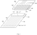
- FIG. 1 is a view illustrating components configured to implement a connection structure according to an embodiment disclosed in the present disclosure.
- FIG. 1 illustrates a connector including the connection structure according to the embodiment disclosed in the present disclosure.
- the connector illustrated in FIG. 1 may have a structure in which a first member 100 and a second member 200 are connected to each other. That is, the connector illustrated in FIG. 1 may have the structure in which the first member 100 and the second member 200 are coupled to each other such that the first member 100 is positioned at an upper end and the second member 200 is positioned at a lower end.
- the connection structure illustrated in FIG. 1 may be applied to an FFC type connector.
- the first member 100 may include a first connection part 110, a first guide part (guide block) 120, a bonding part 130, a conductor pattern 140, and an insulation film 150.
- the second member 200 may include a second connection part 210, a second guide part (guide groove) 220, a PCB 230, a conductive pad 240, and an IC circuit 250.
- the first connection part 110 of the first member 100 may interact with the second connection part 210 of the second member 200 to couple the first member 100 and the second member 200.
- the first connection part 110 may be provided on one surface (e.g., an upper end) of the first member 100
- the second connection part 210 may be provided on the other surface (e.g., a lower end) of the second member 200.
- the positions of the first and second connection parts 110 and 210 are not limited to the positions illustrated in FIG. 1 .
- the first connection part 110 may be positioned at any point on the first member 100
- the second connection part 210 may be positioned at any point on the second member 200.
- At least one of the first and second connection parts 110 and 210 may include an object having magnetism.
- the first connection part 110 may include a ferromagnetic element (e.g., neodymium), and the second connection part 210 may include a steel plate. Therefore, the conductor pattern 140 of the first member 100 and the conductive pad 240 of the second member 200 may be electrically connected to each other by a magnetic force between the first and second connection parts 110 and 210.
- the first guide part 120 of the first member 100 and the second guide part 220 of the second member 200 may be aligned with each other when the first and second members 100 and 200 are coupled.
- the first guide part 120 may be a guide block protruding from the other surface of the first member 100
- the second guide part 220 may be a guide groove formed in one surface of the second member 200 so that the first guide part 120 may be inserted into the guide groove.
- first and second members 100 and 200 may be aligned with each other as the first guide part 120 provided on the first member 100 is coupled to the second guide part 220 provided on the second member 200.
- the shapes of the first and second guide parts 120 and 220 are not limited to the shapes illustrated in FIG. 1 .
- the first and second guide parts 120 and 220 may have various shapes in addition to the shapes illustrated in FIG. 1 .
- the bonding part 130 may attach the first connection part 110 to the first member 100.
- the bonding part 130 may attach the first connection part 110 to the first member 100 such that the first member 100 and the first connection part 110 are attachable to and detachable from each other so that the first connection part 110 may be removed by a jig.
- the bonding part 130 is configured as a magnet.
- One surface of the bonding part 130 may be attached to the first member 100 by a bonding agent (not illustrated), and the other surface of the bonding part 130 may be attached to the first connection part 110 by the magnetic force.
- the conductor pattern 140 may be made of a conductive material and perform a function of transmitting an electrical signal from a device connected to the first member 100. As illustrated in FIG. 1 , the conductor pattern 140 may have a shape including a plurality of conductive wires arranged side by side in the first member 100.
- the insulation film 150 may serve to insulate the conductor patterns 140 included in the first member 100 and protect the conductor patterns 140 from the outside.
- the conductor pattern 140 may have a structure laminated between the two insulation films 150 by a bonding agent (not illustrated). In this case, a portion of the insulation film 150, where the conductor pattern 140 comes into contact with the second member 200, may be removed so that the conductor pattern 140 is electrically connected to the conductive pad 240 of the second member 200.
- the PCB 230 provided on the second member 200 may include the conductive pad 240 and the IC circuit 250.
- the conductive pad 240 is made of a conductive material, such that the conductive pad 240 may receive an electrical signal from the conductor pattern 140 of the first member 100 and transmit the electrical signal to the conductor pattern 140 from a device connected to the second member 200.
- the electrical signal received through the conductive pad 240 may be transmitted through the IC circuit 250 to the device connected to the second member 200.
- connection structure according to the embodiment disclosed in the present disclosure is configured by using the member having magnetism, such as a ferromagnetic element, to reduce costs required to manufacture the connector and make it easy to connect or disconnect the two connection terminals of the connector.
- FIG. 2 is a view illustrating a structure of the member including the connection part for implementing the connection structure according to the embodiment disclosed in the present disclosure.
- FIG. 2(a) is a cross-sectional view taken along line A-A' in FIG. 1 .
- the conductor pattern 140 of the first member 100 may have the shape including the plurality of conductive wires.
- the conductor pattern 140 may be attached to the insulation films 150 by the bonding agent 160.
- the conductor pattern 140 may have the structure laminated between the two insulation films 150.
- FIG. 2(b) illustrates a portion 170 where a part of the insulation film 150 of the first member 100 is removed.
- the portion of the insulation film 150 provided on the other surface of the first member 100 which corresponds to a region of one surface of the second member 200 in which the conductive pad 240 is provided, is removed, such that the conductor pattern 140 of the first member 100 and the conductive pad 240 of the second member 200 may come into physical/electric contact with each other.
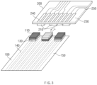
- FIG. 3 is a view illustrating components configured to implement a connection structure according to another embodiment disclosed in the present disclosure.
- the connector illustrated in FIG. 3 may also have the structure in which the first and second members 100 and 200 are connected to each other. That is, the connector may have the structure in which the first member 100 and the second member 200 are coupled to each other such that the first member 100 is positioned at the upper end and the second member 200 is positioned at the lower end.
- the first member 100 may include the first connection part 110, the bonding part 130, the conductor pattern 140, and the insulation film 150.
- the second member 200 may include the second connection part 210, the PCB 230, the conductive pad 240, and the IC circuit 250.
- the first connection part 110, the bonding part 130, the conductor pattern 140, and the insulation film 150 of the first member 100 and the second connection part 210, the PCB 230, the conductive pad 240, and the IC circuit 250 of the second member 200 are substantially identical to those illustrated in FIG. 1 , a detailed description thereof will be omitted in FIG. 3 .
- FIG. 3 does not illustrate the first and second guide parts 120 and 220 for convenience, but the first and second guide parts 120 and 220 may also be included, as necessary.
- first connection part 110 of the first member 100 and the second connection part 210 of the second member 200 are provided in the form of a plurality of blocks as illustrated in FIG. 3 instead of being integrated as illustrated in FIG. 1 .
- the blocks of the first and second connection parts 110 and 210 may be disposed to correspond to one another in a one-to-one manner.
- the plurality of blocks may be disposed so that polarities of two adjacent blocks are opposite to each other.
- the blocks may be repeatedly disposed so that the polarities of the adjacent blocks are opposite to each other, as illustrated in FIG. 3 . As described below, this is to easily release the magnet of the first connection part 110 by means of the jig by blocking an external magnetic force by forming a closed circuit of a magnetic field formed by the first connection part 110.
- FIG. 4 is a view illustrating a jig configured to attach or detach the connection part of the connection structure according to another embodiment disclosed in the present disclosure.
- a jig 300 may include magnet parts 310, a handle 320, and bonding parts 330.
- the jig 300 illustrated in FIG. 4 may attach or detach at least one of the first and second connection parts 110 and 210 by using the magnet part 310 having a polarity opposite to a polarity of at least one of the first and second connection parts 110 and 210 when the magnetic force between the first and second connection parts 110 and 210 is equal to or higher than a reference value (e.g., when it is difficult to directly release the magnet by using a person's effort).
- a reference value e.g., when it is difficult to directly release the magnet by using a person's effort.
- connection structure disclosed in the present disclosure is not limited thereto.
- the second connection part 210 may be a ferromagnetic element, or both the first and second connection parts 110 and 210 may be ferromagnetic elements.
- the magnet parts 310 may be provided to correspond to the plurality of magnet blocks of the first connection part 110 in a one-to-one manner and disposed so that each of the magnet parts 310 has the polarity opposite to the polarity of each of the blocks of the first connection part 110. Therefore, the magnet part 310 may be coupled to the first connection part 110 by the magnetic force.
- the magnet part 310 and the first connection part 110 which have the opposite polarities, are connected to each other by the magnetic force, the closed circuit of the magnetic field is formed, and the external magnetic force is blocked, such that the magnetic force between the first member 100 and the first connection part 110 is eliminated (a magnetic force off region in FIG. 4 ). Therefore, the first connection part 110 may be easily removed from the first member 100 by the jig 300.
- the magnet parts 310 may be attached to the handle 320, and the handle 320 may be formed to be grasped by a user. Therefore, the user may hold the handle 320 and bring the magnet part 310 of the jig 300 into contact with the first connection part 110 of the first member 100 of the connector. Therefore, the user may easily remove the first connection part 110 from the first member 100 even when the user cannot directly release the first connection part 110 because of the high magnetic force between the first and second connection parts 110 and 210.
- the bonding part 330 may attach the magnet part 310 to a lower end of the handle 320 of the jig 300.
- the bonding part 330 may have a sufficient bonding force that enables the first connection part 110 to be detached from the first member 100.
- connection structure according to the embodiment disclosed in the present disclosure is configured by using the member having magnetism, such as a ferromagnetic element, to reduce costs required to manufacture the connector and make it easy to connect or disconnect the two connection terminals of the connector.
Landscapes
- Engineering & Computer Science (AREA)
- Microelectronics & Electronic Packaging (AREA)
- Metallurgy (AREA)
- Manufacturing & Machinery (AREA)
- Details Of Connecting Devices For Male And Female Coupling (AREA)
- Coupling Device And Connection With Printed Circuit (AREA)
Abstract
Description
- This application claims priority to and the benefit of
Korean Patent Application No. 10-2021-0001128 filed in the Korean Intellectual Property Office on January 5, 2021 - Embodiments disclosed in the present disclosure relate to a connection structure of a connector.
- In general, a component, called a connector, is used to connect a plurality of conductive wires or devices through which an electric current flows. The factors, which are associated with connection and disconnection between two connection terminals, are considered important in the connector. In particular, one of the important factors is to reduce costs by simplifying a connecting structure.
- Examples of the connectors representatively include a wire type connector, FFC (flexible flat cable) type connector, and the like. In general, the connector includes therein an injection-molded product configured to constitute a housing, and a mounting structure on which a connector terminal and a PCB (printed circuit board) are mounted. Since the connector has several complicated components to securely couple the two connection terminals as described above, there is a need to minimize the components.
- An object of embodiments disclosed in the present disclosure is to provide a connection structure configured by using a member having magnetism, such as a ferromagnetic element, to reduce costs required to manufacture a connector and make it easy to connect or disconnect two connection terminals of the connector.
- Technical problems of the embodiments disclosed in the present disclosure are not limited to the aforementioned technical problems, and other technical problems, which are not mentioned above, may be clearly understood by those skilled in the art from the following descriptions.
- A connection structure according to an embodiment disclosed in the present disclosure includes: a first connection part provided on one surface of a first member including at least one conductor pattern; and a second connection part provided on the other surface of a second member having at least one conductive pad formed on one surface thereof, the second connection part being configured to be connected to one surface of the first connection part by means of a magnetic force so that at least one conductor pattern and at least one conductive pad are electrically connected to each other.
- According to the embodiment, the first connection part may include a ferromagnetic element, and the second connection part may include a steel plate.
- According to the embodiment, the first member may include a first guide part, the second member may include a second guide part, the first and second guide parts may be aligned with each other as the first and second members are coupled to each other.
- According to the embodiment, the first guide part may include a guide block, the second guide part may include a guide groove, the first and second members may be aligned with each other as the first and second guide parts are coupled to each other.
- According to the embodiment, the first and second connection parts may have a plurality of blocks configured to correspond to one another in a one-to-one manner.
- According to the embodiment, when at least one of the first and second connection parts includes a magnet, the plurality of blocks may be disposed such that polarities of the adjacent blocks are opposite to each other.
- According to the embodiment, the first member may include a film configured to protect the conductor pattern.
- According to the embodiment, a portion of the film, where the first member comes into contact with the second member, may be partially removed.
- According to the embodiment, when a magnetic force between the first and second connection parts is equal to or higher than a reference value, at least one of the first and second connection parts may be attachable or detachable by a jig having a polarity opposite to a polarity of at least one of the first and second connection parts.
- According to the embodiment, the second member may have a structure in which the conductive pad and an IC circuit are provided on a printed circuit board (PCB).
- The connection structure according to the embodiment disclosed in the present disclosure is configured by using the member having magnetism, such as a ferromagnetic element, to reduce costs required to manufacture the connector and make it easy to connect or disconnect the two connection terminals of the connector.
-
-
FIG. 1 is a view illustrating components configured to implement a connection structure according to an embodiment disclosed in the present disclosure. -
FIG. 2 is a view illustrating a structure of a member including a connection part for implementing the connection structure according to the embodiment disclosed in the present disclosure. -
FIG. 3 is a view illustrating components configured to implement a connection structure according to another embodiment disclosed in the present disclosure. -
FIG. 4 is a view illustrating a jig configured to attach or detach the connection part of the connection structure according to another embodiment disclosed in the present disclosure. - Hereinafter, various embodiments disclosed in the present disclosure will be described in detail with reference to the accompanying drawings. In the drawings of the present disclosure, the same constituent elements will be designated by the same reference numerals, and the repetitive description of the same constituent elements will be omitted.
- Specific structural or functional descriptions of various embodiments disclosed in the present disclosure are exemplified only for the purpose of explaining the embodiments, the embodiments disclosed in the present disclosure may be carried out in various forms, and it should not be interpreted that the present disclosure is limited to the embodiments described in the present disclosure.
- The terms "first" and "second" used in various embodiments may be used regardless of the order and/or importance of various constituent elements and do not limit the corresponding constituent elements. For example, a first constituent element may be named a second constituent element, and similarly, the second constituent element may also be named the first constituent element, without departing from the scope of the embodiment disclosed in the present disclosure.
- The terms used in the present disclosure are used to just describe a specific embodiment and do not intend to limit the scope of another embodiment. Singular expressions may include plural expressions unless clearly described as different meanings in the context.
- All terms used herein, including technical or scientific terms, may have the same meaning as commonly understood by those skilled in the art to which the embodiments disclosed in the present disclosure pertain. The terms such as those defined in a commonly used dictionary may be interpreted as having meanings identical or similar to meanings in the context of related technologies and should not be interpreted as ideal or excessively formal meanings unless explicitly defined in the present disclosure. In some instances, the terms defined in the present disclosure should not be interpreted to exclude the embodiments disclosed in the present disclosure.
-
FIG. 1 is a view illustrating components configured to implement a connection structure according to an embodiment disclosed in the present disclosure. -
FIG. 1 illustrates a connector including the connection structure according to the embodiment disclosed in the present disclosure. The connector illustrated inFIG. 1 may have a structure in which afirst member 100 and asecond member 200 are connected to each other. That is, the connector illustrated inFIG. 1 may have the structure in which thefirst member 100 and thesecond member 200 are coupled to each other such that thefirst member 100 is positioned at an upper end and thesecond member 200 is positioned at a lower end. For example, the connection structure illustrated inFIG. 1 may be applied to an FFC type connector. - In this case, the
first member 100 may include afirst connection part 110, a first guide part (guide block) 120, abonding part 130, aconductor pattern 140, and aninsulation film 150. In addition, thesecond member 200 may include asecond connection part 210, a second guide part (guide groove) 220, aPCB 230, aconductive pad 240, and anIC circuit 250. - The
first connection part 110 of thefirst member 100 may interact with thesecond connection part 210 of thesecond member 200 to couple thefirst member 100 and thesecond member 200. In this case, as illustrated inFIG. 1 , thefirst connection part 110 may be provided on one surface (e.g., an upper end) of thefirst member 100, and thesecond connection part 210 may be provided on the other surface (e.g., a lower end) of thesecond member 200. However, the positions of the first andsecond connection parts FIG. 1 . Thefirst connection part 110 may be positioned at any point on thefirst member 100, and thesecond connection part 210 may be positioned at any point on thesecond member 200. - At least one of the first and
second connection parts first connection part 110 may include a ferromagnetic element (e.g., neodymium), and thesecond connection part 210 may include a steel plate. Therefore, theconductor pattern 140 of thefirst member 100 and theconductive pad 240 of thesecond member 200 may be electrically connected to each other by a magnetic force between the first andsecond connection parts - The
first guide part 120 of thefirst member 100 and thesecond guide part 220 of thesecond member 200 may be aligned with each other when the first andsecond members FIG. 1 , thefirst guide part 120 may be a guide block protruding from the other surface of thefirst member 100, and thesecond guide part 220 may be a guide groove formed in one surface of thesecond member 200 so that thefirst guide part 120 may be inserted into the guide groove. - As described above, the first and
second members first guide part 120 provided on thefirst member 100 is coupled to thesecond guide part 220 provided on thesecond member 200. However, the shapes of the first andsecond guide parts FIG. 1 . The first andsecond guide parts FIG. 1 . - The bonding
part 130 may attach thefirst connection part 110 to thefirst member 100. In this case, as described above, thebonding part 130 may attach thefirst connection part 110 to thefirst member 100 such that thefirst member 100 and thefirst connection part 110 are attachable to and detachable from each other so that thefirst connection part 110 may be removed by a jig. For example, thebonding part 130 is configured as a magnet. One surface of thebonding part 130 may be attached to thefirst member 100 by a bonding agent (not illustrated), and the other surface of thebonding part 130 may be attached to thefirst connection part 110 by the magnetic force. - The
conductor pattern 140 may be made of a conductive material and perform a function of transmitting an electrical signal from a device connected to thefirst member 100. As illustrated inFIG. 1 , theconductor pattern 140 may have a shape including a plurality of conductive wires arranged side by side in thefirst member 100. - The
insulation film 150 may serve to insulate theconductor patterns 140 included in thefirst member 100 and protect theconductor patterns 140 from the outside. In this case, theconductor pattern 140 may have a structure laminated between the twoinsulation films 150 by a bonding agent (not illustrated). In this case, a portion of theinsulation film 150, where theconductor pattern 140 comes into contact with thesecond member 200, may be removed so that theconductor pattern 140 is electrically connected to theconductive pad 240 of thesecond member 200. - The
PCB 230 provided on thesecond member 200 may include theconductive pad 240 and theIC circuit 250. Theconductive pad 240 is made of a conductive material, such that theconductive pad 240 may receive an electrical signal from theconductor pattern 140 of thefirst member 100 and transmit the electrical signal to theconductor pattern 140 from a device connected to thesecond member 200. In addition, the electrical signal received through theconductive pad 240 may be transmitted through theIC circuit 250 to the device connected to thesecond member 200. - As described above, the connection structure according to the embodiment disclosed in the present disclosure is configured by using the member having magnetism, such as a ferromagnetic element, to reduce costs required to manufacture the connector and make it easy to connect or disconnect the two connection terminals of the connector.
-
FIG. 2 is a view illustrating a structure of the member including the connection part for implementing the connection structure according to the embodiment disclosed in the present disclosure. -
FIG. 2(a) is a cross-sectional view taken along line A-A' inFIG. 1 . In this case, as illustrated inFIG. 1 , theconductor pattern 140 of thefirst member 100 may have the shape including the plurality of conductive wires. In addition, theconductor pattern 140 may be attached to theinsulation films 150 by thebonding agent 160. As illustrated inFIG. 2(a) , theconductor pattern 140 may have the structure laminated between the twoinsulation films 150. -
FIG. 2(b) illustrates aportion 170 where a part of theinsulation film 150 of thefirst member 100 is removed. The portion of theinsulation film 150, where theconductor pattern 140 of thefirst member 100 comes into contact with theconductive pad 240 of thesecond member 200, is removed so that theconductor pattern 140 of thefirst member 100 comes into contact with theconductive pad 240 of thesecond member 200. - That is, referring to
FIG. 1 , the portion of theinsulation film 150 provided on the other surface of thefirst member 100, which corresponds to a region of one surface of thesecond member 200 in which theconductive pad 240 is provided, is removed, such that theconductor pattern 140 of thefirst member 100 and theconductive pad 240 of thesecond member 200 may come into physical/electric contact with each other. -
FIG. 3 is a view illustrating components configured to implement a connection structure according to another embodiment disclosed in the present disclosure. Like the connector illustrated inFIG. 1 , the connector illustrated inFIG. 3 may also have the structure in which the first andsecond members first member 100 and thesecond member 200 are coupled to each other such that thefirst member 100 is positioned at the upper end and thesecond member 200 is positioned at the lower end. - Even in this case, the
first member 100 may include thefirst connection part 110, thebonding part 130, theconductor pattern 140, and theinsulation film 150. In addition, thesecond member 200 may include thesecond connection part 210, thePCB 230, theconductive pad 240, and theIC circuit 250. In this case, because thefirst connection part 110, thebonding part 130, theconductor pattern 140, and theinsulation film 150 of thefirst member 100 and thesecond connection part 210, thePCB 230, theconductive pad 240, and theIC circuit 250 of thesecond member 200 are substantially identical to those illustrated inFIG. 1 , a detailed description thereof will be omitted inFIG. 3 . In addition,FIG. 3 does not illustrate the first andsecond guide parts second guide parts - There is a difference in that the
first connection part 110 of thefirst member 100 and thesecond connection part 210 of thesecond member 200 are provided in the form of a plurality of blocks as illustrated inFIG. 3 instead of being integrated as illustrated inFIG. 1 . In this case, the blocks of the first andsecond connection parts - In addition, when at least one of the first and
second connection parts first connection part 110 is a ferromagnetic element, the blocks may be repeatedly disposed so that the polarities of the adjacent blocks are opposite to each other, as illustrated inFIG. 3 . As described below, this is to easily release the magnet of thefirst connection part 110 by means of the jig by blocking an external magnetic force by forming a closed circuit of a magnetic field formed by thefirst connection part 110. -
FIG. 4 is a view illustrating a jig configured to attach or detach the connection part of the connection structure according to another embodiment disclosed in the present disclosure. - Referring to
FIG. 4 , ajig 300 according to the embodiment disclosed in the present disclosure may includemagnet parts 310, ahandle 320, andbonding parts 330. In particular, thejig 300 illustrated inFIG. 4 may attach or detach at least one of the first andsecond connection parts magnet part 310 having a polarity opposite to a polarity of at least one of the first andsecond connection parts second connection parts - In addition, the configuration in which the
first connection part 110 provided on thefirst member 100 is a ferromagnetic element will be described with reference toFIG. 4 . However, the connection structure disclosed in the present disclosure is not limited thereto. Thesecond connection part 210 may be a ferromagnetic element, or both the first andsecond connection parts - The
magnet parts 310 may be provided to correspond to the plurality of magnet blocks of thefirst connection part 110 in a one-to-one manner and disposed so that each of themagnet parts 310 has the polarity opposite to the polarity of each of the blocks of thefirst connection part 110. Therefore, themagnet part 310 may be coupled to thefirst connection part 110 by the magnetic force. When themagnet part 310 and thefirst connection part 110, which have the opposite polarities, are connected to each other by the magnetic force, the closed circuit of the magnetic field is formed, and the external magnetic force is blocked, such that the magnetic force between thefirst member 100 and thefirst connection part 110 is eliminated (a magnetic force off region inFIG. 4 ). Therefore, thefirst connection part 110 may be easily removed from thefirst member 100 by thejig 300. - The
magnet parts 310 may be attached to thehandle 320, and thehandle 320 may be formed to be grasped by a user. Therefore, the user may hold thehandle 320 and bring themagnet part 310 of thejig 300 into contact with thefirst connection part 110 of thefirst member 100 of the connector. Therefore, the user may easily remove thefirst connection part 110 from thefirst member 100 even when the user cannot directly release thefirst connection part 110 because of the high magnetic force between the first andsecond connection parts - The
bonding part 330 may attach themagnet part 310 to a lower end of thehandle 320 of thejig 300. In this case, thebonding part 330 may have a sufficient bonding force that enables thefirst connection part 110 to be detached from thefirst member 100. - As described above, the connection structure according to the embodiment disclosed in the present disclosure is configured by using the member having magnetism, such as a ferromagnetic element, to reduce costs required to manufacture the connector and make it easy to connect or disconnect the two connection terminals of the connector.
- All the constituent elements, which constitute the embodiment disclosed in the present disclosure described above, may be integrally coupled or operate by being combined, but the embodiments disclosed in the present disclosure are not necessarily limited to the embodiment. That is, one or more of the constituent elements may be selectively combined and operated within the object of the embodiments disclosed in the present disclosure.
- In addition, unless explicitly described to the contrary, the words "comprise," "include," or "have" and variations such as "comprises," "comprising," "includes," "including," has," or "having," should be understood to imply the inclusion of stated elements but not the exclusion of any other elements. Unless otherwise defined, all terms including technical or scientific terms may have the same meaning as commonly understood by those skilled in the art to which the embodiments disclosed in the present disclosure pertain. The terms such as those defined in a commonly used dictionary may be interpreted as having meanings consistent with meanings in the context of related technologies and may not be interpreted as ideal or excessively formal meanings unless explicitly defined in the present disclosure.
- The above description is simply given for illustratively describing the technical spirit disclosed in the present embodiment, and those skilled in the art to which the embodiments disclosed in the present disclosure pertain will appreciate that various changes and modifications are possible without departing from the essential characteristics of the embodiments disclosed in the present disclosure. Therefore, the embodiments disclosed in the present disclosure are provided for illustrative purposes only but not intended to limit the technical concept of the embodiments disclosed in the present disclosure. The scope of the technical spirit disclosed in the present disclosure is not limited by the embodiment. The protective scope of the technical spirit disclosed in the present disclosure should be construed based on the appended claims, and all the technical spirit in the equivalent scope thereto should be construed as falling within the scope of the present disclosure.
Claims (10)
- A connection structure comprising:a first connection part provided on one surface of a first member including at least one conductor pattern; anda second connection part provided on the other surface of a second member having at least one conductive pad formed on one surface thereof, the second connection part being configured to be connected to one surface of the first connection part by means of a magnetic force so that at least one conductor pattern and at least one conductive pad are electrically connected to each other.
- The connection structure of claim 1, wherein the first connection part comprises a ferromagnetic element, and the second connection part comprises a steel plate.
- The connection structure of claim 1, wherein the first member comprises a first guide part, the second member comprises a second guide part, the first and second guide parts are aligned with each other as the first and second members are coupled to each other.
- The connection structure of claim 3, wherein the first guide part comprises a guide block, the second guide part comprises a guide groove, the first and second members are aligned with each other as the first and second guide parts are coupled to each other.
- The connection structure of claim 1, wherein the first and second connection parts have a plurality of blocks configured to correspond to one another in a one-to-one manner.
- The connection structure of claim 5, wherein when at least one of the first and second connection parts comprises a magnet, the plurality of blocks is disposed such that polarities of the adjacent blocks are opposite to each other.
- The connection structure of claim 1, wherein the first member comprises a film configured to protect the conductor pattern.
- The connection structure of claim 7, wherein a portion of the film, where the first member comes into contact with the second member, is partially removed.
- The connection structure of claim 1, wherein when a magnetic force between the first and second connection parts is equal to or higher than a reference value, at least one of the first and second connection parts is attachable or detachable by a jig having a polarity opposite to a polarity of at least one of the first and second connection parts.
- The connection structure of claim 1, wherein the second member has a structure in which the conductive pad and an IC circuit are provided on a printed circuit board (PCB).
Applications Claiming Priority (2)
| Application Number | Priority Date | Filing Date | Title |
|---|---|---|---|
| KR1020210001128A KR102790199B1 (en) | 2021-01-05 | 2021-01-05 | Connection structure |
| PCT/KR2021/018553 WO2022149743A1 (en) | 2021-01-05 | 2021-12-08 | Connection structure |
Publications (3)
| Publication Number | Publication Date |
|---|---|
| EP4203199A1 true EP4203199A1 (en) | 2023-06-28 |
| EP4203199A4 EP4203199A4 (en) | 2024-03-13 |
| EP4203199B1 EP4203199B1 (en) | 2026-04-22 |
Family
ID=82357214
Family Applications (1)
| Application Number | Title | Priority Date | Filing Date |
|---|---|---|---|
| EP21917905.8A Active EP4203199B1 (en) | 2021-01-05 | 2021-12-08 | Connection structure |
Country Status (6)
| Country | Link |
|---|---|
| US (1) | US12489245B2 (en) |
| EP (1) | EP4203199B1 (en) |
| JP (1) | JP7517759B2 (en) |
| KR (1) | KR102790199B1 (en) |
| CN (1) | CN116325379B (en) |
| WO (1) | WO2022149743A1 (en) |
Families Citing this family (1)
| Publication number | Priority date | Publication date | Assignee | Title |
|---|---|---|---|---|
| KR102790199B1 (en) * | 2021-01-05 | 2025-04-03 | 주식회사 엘지에너지솔루션 | Connection structure |
Family Cites Families (76)
| Publication number | Priority date | Publication date | Assignee | Title |
|---|---|---|---|---|
| US3245024A (en) * | 1962-03-23 | 1966-04-05 | Evans William Robert | Separable electrical connector for plural conductors |
| US3786391A (en) * | 1972-07-11 | 1974-01-15 | W Mathauser | Magnetic self-aligning electrical connector |
| US4737112A (en) * | 1986-09-05 | 1988-04-12 | American Telephone And Telegraph Company, At&T Bell Laboratories | Anisotropically conductive composite medium |
| US4713014A (en) * | 1986-12-23 | 1987-12-15 | Hughes Aircraft Company | Quick-release multi-module terminating assembly |
| US5036128A (en) * | 1987-02-06 | 1991-07-30 | Key-Tech, Inc. | Printed circuit board |
| US4960614A (en) * | 1987-02-06 | 1990-10-02 | Key-Tech, Inc. | Printed circuit board |
| JPH01128586A (en) * | 1987-11-13 | 1989-05-22 | Ricoh Co Ltd | Printed circuit board connection method |
| JP2746763B2 (en) * | 1991-02-18 | 1998-05-06 | シャープ株式会社 | Burn-in apparatus and burn-in method using the same |
| JPH04282582A (en) * | 1991-03-09 | 1992-10-07 | Canon Inc | Method of connecting electric circuit parts |
| JPH0766844B2 (en) | 1991-12-13 | 1995-07-19 | 株式会社フジソク | Connector device and its contact device |
| US6528873B1 (en) * | 1996-01-16 | 2003-03-04 | Texas Instruments Incorporated | Ball grid assembly with solder columns |
| US5795162A (en) * | 1996-03-28 | 1998-08-18 | Lucent Technologies, Inc. | RF flex circuit transmission line and interconnection method |
| EP0977215A3 (en) * | 1996-08-09 | 2000-12-06 | SUMITOMO WIRING SYSTEMS, Ltd. | Charging connector for electric vehicle |
| KR100231152B1 (en) * | 1996-11-26 | 1999-11-15 | 윤종용 | Mounting method for mounting ic on pcb |
| JP3817815B2 (en) * | 1997-03-11 | 2006-09-06 | 住友電気工業株式会社 | Electromagnetic connector |
| DE19726419A1 (en) * | 1997-06-23 | 1999-01-28 | Daimler Benz Aerospace Airbus | Heating conductor connection system in an aircraft |
| JP3451393B2 (en) * | 1998-01-30 | 2003-09-29 | 日本航空電子工業株式会社 | Plug connector and socket connector |
| US6492738B2 (en) * | 1999-09-02 | 2002-12-10 | Micron Technology, Inc. | Apparatus and methods of testing and assembling bumped devices using an anisotropically conductive layer |
| ES2290797T3 (en) * | 2001-06-01 | 2008-02-16 | Covidien Ag | CABLE CONNECTOR WITH A RETURN PAD. |
| DE10242645A1 (en) * | 2002-09-13 | 2004-03-25 | Magcode Ag | Method of creating electrical connection to modules e.g. in motor vehicle, by using magnetic bodies in current providing unit and current receiving unit to form contact automatically |
| JP2004296426A (en) * | 2003-03-07 | 2004-10-21 | Japan Aviation Electronics Industry Ltd | Magnet connector |
| US20040209489A1 (en) * | 2003-04-21 | 2004-10-21 | Clapper Edward O. | Apparatus for automatic docking |
| US7252512B2 (en) * | 2004-04-21 | 2007-08-07 | Japan Aviation Electronics Industry, Limited | Self-alignment magnetic connector reduced in size |
| US7331793B2 (en) * | 2005-12-16 | 2008-02-19 | Motorola, Inc. | Magnetic connector |
| US20070254510A1 (en) * | 2006-04-27 | 2007-11-01 | Debey Henry C | Magnetically Retained Electrical Connector |
| US7611357B2 (en) * | 2006-09-15 | 2009-11-03 | Mr Board, Inc. | Magnetic component connector, circuit boards for use therewith, and kits for building and designing circuits |
| US8650925B2 (en) * | 2007-01-05 | 2014-02-18 | Apple Inc. | Extrusion method for fabricating a compact tube with internal features |
| ATE554517T1 (en) * | 2007-01-06 | 2012-05-15 | Apple Inc | HEADSET CONNECTOR FOR SELECTIVE CONNECTION OF SIGNALS DEPENDING ON THE PARTICULAR ORIENTATION OF THE CONNECTED CONNECTOR |
| JP4849681B2 (en) | 2007-03-22 | 2012-01-11 | 日本航空電子工業株式会社 | Magnetic connector |
| KR20090022877A (en) * | 2007-08-31 | 2009-03-04 | 주식회사 탑 엔지니어링 | Method for manufacturing thin film metal conductor |
| JP5171365B2 (en) * | 2008-04-11 | 2013-03-27 | 中国電力株式会社 | Plug connector |
| US9300081B2 (en) * | 2010-02-02 | 2016-03-29 | Charles Albert Rudisill | Interposer connectors with magnetic components |
| WO2012019231A1 (en) * | 2010-08-13 | 2012-02-16 | Cathrx Ltd | A catheter electrical connector assembly |
| DK201070422A (en) * | 2010-10-01 | 2010-10-05 | Goel Anil | Zero no-load USB power supply and a method for controlling the power consumption of a USB power supply |
| US9442339B2 (en) * | 2010-12-08 | 2016-09-13 | View, Inc. | Spacers and connectors for insulated glass units |
| US9735500B2 (en) * | 2012-07-31 | 2017-08-15 | Hewlett-Packard Development Company, L.P. | Magnetic connector for a computing device |
| US9130291B2 (en) * | 2012-08-29 | 2015-09-08 | Hewlett-Packard Development Company, Lp. | Device connector including magnet |
| US8758025B1 (en) * | 2012-09-10 | 2014-06-24 | Amazon Technologies, Inc. | Systems and methods for facilitating a connection |
| KR101945250B1 (en) | 2012-12-14 | 2019-02-07 | 삼성전자 주식회사 | Connecting Interface and Connector of Electronic Device, Connecting System including the same, and Operating Method thereof |
| DE202013101011U1 (en) * | 2013-03-08 | 2013-03-18 | Rosenberger Hochfrequenztechnik Gmbh & Co. Kg | Magnetic plug connection |
| CN203445280U (en) * | 2013-07-26 | 2014-02-19 | 富士康(昆山)电脑接插件有限公司 | Electric connector |
| US20150094713A1 (en) * | 2013-09-30 | 2015-04-02 | Covidien Lp | Systems and methods for electrical coupling in a medical device |
| WO2015070321A1 (en) * | 2013-11-13 | 2015-05-21 | Szeto Timothy Jing Yin | Magnetic connectors |
| CN206480799U (en) * | 2014-02-19 | 2017-09-08 | 莫列斯有限公司 | connecting device |
| JP6293521B2 (en) * | 2014-03-07 | 2018-03-14 | 日本航空電子工業株式会社 | Magnet connector |
| KR101674593B1 (en) | 2014-11-21 | 2016-11-09 | 서동진 | Connector using a magnet |
| KR102360490B1 (en) * | 2014-12-24 | 2022-02-09 | 삼성전자주식회사 | An electric connector |
| EP3104671B1 (en) * | 2015-05-08 | 2018-07-18 | Joylabz LLC | Methods and systems for magnetic coupling |
| KR102478668B1 (en) | 2015-10-06 | 2022-12-16 | 엘지디스플레이 주식회사 | Connector and electronic device having therreof |
| KR20170077604A (en) * | 2015-12-28 | 2017-07-06 | 엘지디스플레이 주식회사 | Flexible cable connector and display device having the same |
| KR20170096748A (en) * | 2016-02-17 | 2017-08-25 | 김영선 | Magnetic Snap connector embedded in wearable device |
| KR101805446B1 (en) * | 2016-09-22 | 2017-12-07 | 에스케이테크엑스 주식회사 | Connector attached by magnetic force and control method thereof |
| US11121502B2 (en) * | 2016-09-23 | 2021-09-14 | Apple Inc. | Magnetic connectors |
| JP7224285B2 (en) * | 2016-12-09 | 2023-02-17 | ルミレッズ ホールディング ベーフェー | Method for manufacturing LED carrier assembly |
| CN108879191B (en) * | 2017-05-08 | 2021-03-23 | 富士康(昆山)电脑接插件有限公司 | Plug connector |
| US10381760B2 (en) * | 2018-01-05 | 2019-08-13 | Hamilton Sundstrand Corporation | Printed circuit board edge electrical contact pads |
| KR102404752B1 (en) * | 2018-01-25 | 2022-05-31 | 주식회사 엘지에너지솔루션 | Flat Cable having the improved function of preventing short-circuit |
| EP3760014B1 (en) | 2018-02-28 | 2022-09-28 | Raytheon Company | Snap-rf interconnections |
| KR102134864B1 (en) * | 2018-08-03 | 2020-07-16 | 국방과학연구소 | Implantable cable assembly |
| US11488764B2 (en) * | 2018-10-09 | 2022-11-01 | Delta Electronics, Inc. | Voltage regulator module |
| EP3637963B1 (en) * | 2018-10-12 | 2024-02-07 | AT&S Austria Technologie & Systemtechnik Aktiengesellschaft | Component carrier structures connected by cooperating magnet structures |
| KR102167507B1 (en) | 2018-10-15 | 2020-10-20 | 주식회사 좋은사람들 | Connector for smart clothe |
| US10594074B1 (en) * | 2018-10-30 | 2020-03-17 | Microsoft Technology Licensing, Llc | Shielded magnetic electronic connector |
| KR102326081B1 (en) * | 2018-11-13 | 2021-11-11 | 주식회사 엘지에너지솔루션 | Flexible Printed Circuit connection structure and Printed Circuit Board connection method using the same |
| KR102148179B1 (en) * | 2018-11-28 | 2020-08-26 | 지엔에스티 주식회사 | Connector assembly |
| US10944226B2 (en) * | 2019-01-23 | 2021-03-09 | Dell Products L.P. | Connector system for charging a device using a charging receptacle |
| KR20200117165A (en) * | 2019-04-03 | 2020-10-14 | 주식회사 아모센스 | Flexible Cable Jumper Apparatus and Manufacturing Method For The Same |
| KR102447684B1 (en) | 2019-06-27 | 2022-09-27 | 주식회사 노바텍 | Circuit board on which single magnet part is installed and method of installing single magnet using surface mount technology device |
| KR102099966B1 (en) | 2019-08-28 | 2020-04-13 | 주식회사 한승 | LED Bulb with Reflector |
| CN211404884U (en) | 2020-01-20 | 2020-09-01 | 深圳市拓普联科技术股份有限公司 | Magnetic male and female end connector |
| KR102768404B1 (en) * | 2020-07-22 | 2025-02-17 | 주식회사 엘지에너지솔루션 | Connector structure including magnet |
| KR102790199B1 (en) * | 2021-01-05 | 2025-04-03 | 주식회사 엘지에너지솔루션 | Connection structure |
| KR20220117387A (en) * | 2021-02-15 | 2022-08-24 | 삼성디스플레이 주식회사 | Display device and method of manufacturing the same |
| KR102733414B1 (en) * | 2021-04-28 | 2024-11-21 | 주식회사 엘지에너지솔루션 | Connector |
| JP7597449B2 (en) * | 2021-07-28 | 2024-12-10 | 新光電気工業株式会社 | Circuit boards, circuit modules |
| US20240322485A1 (en) * | 2023-03-20 | 2024-09-26 | Broadata Communications, Inc. | Self-aligning magnetically coupled connector |
-
2021
- 2021-01-05 KR KR1020210001128A patent/KR102790199B1/en active Active
- 2021-12-08 US US18/031,086 patent/US12489245B2/en active Active
- 2021-12-08 EP EP21917905.8A patent/EP4203199B1/en active Active
- 2021-12-08 JP JP2023519057A patent/JP7517759B2/en active Active
- 2021-12-08 WO PCT/KR2021/018553 patent/WO2022149743A1/en not_active Ceased
- 2021-12-08 CN CN202180068914.XA patent/CN116325379B/en active Active
Also Published As
| Publication number | Publication date |
|---|---|
| CN116325379A (en) | 2023-06-23 |
| US20230378687A1 (en) | 2023-11-23 |
| JP2023544536A (en) | 2023-10-24 |
| WO2022149743A1 (en) | 2022-07-14 |
| CN116325379B (en) | 2026-05-08 |
| KR102790199B1 (en) | 2025-04-03 |
| KR20220099059A (en) | 2022-07-12 |
| EP4203199B1 (en) | 2026-04-22 |
| US12489245B2 (en) | 2025-12-02 |
| JP7517759B2 (en) | 2024-07-17 |
| EP4203199A4 (en) | 2024-03-13 |
Similar Documents
| Publication | Publication Date | Title |
|---|---|---|
| KR200473045Y1 (en) | A double contact point switch and a magnetic connector having the double contact point switch | |
| US9300081B2 (en) | Interposer connectors with magnetic components | |
| US12142881B2 (en) | Charging socket with interface | |
| US7607920B1 (en) | Connecting device for interconnecting electronic devices | |
| US20150081944A1 (en) | Usb memory having non-insertion type connector and gender connected thereto | |
| KR20140115817A (en) | Magnetic connecting device | |
| US6733319B1 (en) | Connector and method for establishing solderfree connections between a rigid main PCB and associated conductors | |
| US20220320775A1 (en) | Connector and wiring structure | |
| JP2005531119A (en) | Electrical connector with wire processing module | |
| EP2705576B1 (en) | High-voltage resistance and retention of printed flex circuits | |
| JP2020149969A (en) | Terminal position guarantee member with multiple latches | |
| US20150062828A1 (en) | Connector, connector Assembly, and Wireless Communication Module | |
| US12489245B2 (en) | Electrical connection structure using magnetic attraction | |
| US8664553B2 (en) | Switch device and connector | |
| US20160322857A1 (en) | Coil, non-contact power receiving apparatus, and portable electronic device | |
| CN106410541A (en) | Electrical connector assembly | |
| WO2008001453A1 (en) | Coaxial cable connector | |
| KR102059134B1 (en) | Magnetic connecting device | |
| EP3309898A1 (en) | Antenna module for millimeter-wave communication systems and transceiver arrangement | |
| KR102472688B1 (en) | Plug connector, socket connector and electrical connector assembly | |
| KR100537544B1 (en) | Planar connector | |
| CN218632501U (en) | FPC wire end connector | |
| CN213071490U (en) | Rubber core of terminal connector | |
| JP2636151B2 (en) | Attach pin jack to circuit board | |
| CN118339722A (en) | Connector equipment and electronic equipment |
Legal Events
| Date | Code | Title | Description |
|---|---|---|---|
| STAA | Information on the status of an ep patent application or granted ep patent |
Free format text: STATUS: THE INTERNATIONAL PUBLICATION HAS BEEN MADE |
|
| PUAI | Public reference made under article 153(3) epc to a published international application that has entered the european phase |
Free format text: ORIGINAL CODE: 0009012 |
|
| STAA | Information on the status of an ep patent application or granted ep patent |
Free format text: STATUS: REQUEST FOR EXAMINATION WAS MADE |
|
| 17P | Request for examination filed |
Effective date: 20230321 |
|
| AK | Designated contracting states |
Kind code of ref document: A1 Designated state(s): AL AT BE BG CH CY CZ DE DK EE ES FI FR GB GR HR HU IE IS IT LI LT LU LV MC MK MT NL NO PL PT RO RS SE SI SK SM TR |
|
| A4 | Supplementary search report drawn up and despatched |
Effective date: 20240213 |
|
| RIC1 | Information provided on ipc code assigned before grant |
Ipc: H01R 13/629 20060101ALN20240207BHEP Ipc: H05K 1/11 20060101ALN20240207BHEP Ipc: H01R 12/79 20110101ALN20240207BHEP Ipc: H05K 3/32 20060101ALI20240207BHEP Ipc: H01R 11/30 20060101ALI20240207BHEP Ipc: H01R 13/62 20060101AFI20240207BHEP |
|
| DAV | Request for validation of the european patent (deleted) | ||
| DAX | Request for extension of the european patent (deleted) | ||
| STAA | Information on the status of an ep patent application or granted ep patent |
Free format text: STATUS: EXAMINATION IS IN PROGRESS |
|
| 17Q | First examination report despatched |
Effective date: 20250604 |
|
| GRAP | Despatch of communication of intention to grant a patent |
Free format text: ORIGINAL CODE: EPIDOSNIGR1 |
|
| STAA | Information on the status of an ep patent application or granted ep patent |
Free format text: STATUS: GRANT OF PATENT IS INTENDED |
|
| INTG | Intention to grant announced |
Effective date: 20251125 |
|
| RIC1 | Information provided on ipc code assigned before grant |
Ipc: H01R 13/62 20060101AFI20251114BHEP Ipc: H01R 11/30 20060101ALI20251114BHEP Ipc: H05K 3/32 20060101ALI20251114BHEP Ipc: H01R 12/79 20110101ALN20251114BHEP Ipc: H05K 1/11 20060101ALN20251114BHEP Ipc: H01R 13/629 20060101ALN20251114BHEP |
|
| GRAS | Grant fee paid |
Free format text: ORIGINAL CODE: EPIDOSNIGR3 |
|
| GRAA | (expected) grant |
Free format text: ORIGINAL CODE: 0009210 |
|
| STAA | Information on the status of an ep patent application or granted ep patent |
Free format text: STATUS: THE PATENT HAS BEEN GRANTED |
|
| P01 | Opt-out of the competence of the unified patent court (upc) registered |
Free format text: CASE NUMBER: UPC_APP_0005730_4203199/2026 Effective date: 20260217 |
|
| AK | Designated contracting states |
Kind code of ref document: B1 Designated state(s): AL AT BE BG CH CY CZ DE DK EE ES FI FR GB GR HR HU IE IS IT LI LT LU LV MC MK MT NL NO PL PT RO RS SE SI SK SM TR |
|
| REG | Reference to a national code |
Ref country code: CH Ref legal event code: F10 Free format text: ST27 STATUS EVENT CODE: U-0-0-F10-F00 (AS PROVIDED BY THE NATIONAL OFFICE) Effective date: 20260422 Ref country code: GB Ref legal event code: FG4D |