EP4203178A1 - An antenna, a wireless communication module, a main board and a computer device - Google Patents
An antenna, a wireless communication module, a main board and a computer device Download PDFInfo
- Publication number
- EP4203178A1 EP4203178A1 EP21216715.9A EP21216715A EP4203178A1 EP 4203178 A1 EP4203178 A1 EP 4203178A1 EP 21216715 A EP21216715 A EP 21216715A EP 4203178 A1 EP4203178 A1 EP 4203178A1
- Authority
- EP
- European Patent Office
- Prior art keywords
- antenna
- wireless communication
- module
- communication module
- printed circuit
- Prior art date
- Legal status (The legal status is an assumption and is not a legal conclusion. Google has not performed a legal analysis and makes no representation as to the accuracy of the status listed.)
- Pending
Links
- 238000004891 communication Methods 0.000 title claims description 80
- 239000004020 conductor Substances 0.000 claims abstract description 19
- 239000000758 substrate Substances 0.000 claims abstract description 19
- 239000012212 insulator Substances 0.000 claims description 20
- 238000000034 method Methods 0.000 description 20
- 230000006870 function Effects 0.000 description 7
- 230000001419 dependent effect Effects 0.000 description 5
- 230000008878 coupling Effects 0.000 description 3
- 238000010168 coupling process Methods 0.000 description 3
- 238000005859 coupling reaction Methods 0.000 description 3
- 238000002955 isolation Methods 0.000 description 3
- 238000004519 manufacturing process Methods 0.000 description 3
- 238000003491 array Methods 0.000 description 2
- 238000013500 data storage Methods 0.000 description 2
- 239000011888 foil Substances 0.000 description 2
- 230000007774 longterm Effects 0.000 description 2
- 239000000463 material Substances 0.000 description 2
- 229920003023 plastic Polymers 0.000 description 2
- 230000035939 shock Effects 0.000 description 2
- ZGHQUYZPMWMLBM-UHFFFAOYSA-N 1,2-dichloro-4-phenylbenzene Chemical compound C1=C(Cl)C(Cl)=CC=C1C1=CC=CC=C1 ZGHQUYZPMWMLBM-UHFFFAOYSA-N 0.000 description 1
- LVROLHVSYNLFBE-UHFFFAOYSA-N 2,3,6-trichlorobiphenyl Chemical compound ClC1=CC=C(Cl)C(C=2C=CC=CC=2)=C1Cl LVROLHVSYNLFBE-UHFFFAOYSA-N 0.000 description 1
- 229920000954 Polyglycolide Polymers 0.000 description 1
- 238000010521 absorption reaction Methods 0.000 description 1
- 230000005540 biological transmission Effects 0.000 description 1
- 238000005352 clarification Methods 0.000 description 1
- 230000001010 compromised effect Effects 0.000 description 1
- 230000005670 electromagnetic radiation Effects 0.000 description 1
- 238000012986 modification Methods 0.000 description 1
- 230000004048 modification Effects 0.000 description 1
- 229920000747 poly(lactic acid) Polymers 0.000 description 1
- 238000012545 processing Methods 0.000 description 1
- 235000010409 propane-1,2-diol alginate Nutrition 0.000 description 1
- 239000004065 semiconductor Substances 0.000 description 1
- 239000007787 solid Substances 0.000 description 1
- 230000033772 system development Effects 0.000 description 1
- 238000012546 transfer Methods 0.000 description 1
Images



Classifications
-
- H—ELECTRICITY
- H01—ELECTRIC ELEMENTS
- H01Q—ANTENNAS, i.e. RADIO AERIALS
- H01Q1/00—Details of, or arrangements associated with, antennas
- H01Q1/12—Supports; Mounting means
- H01Q1/22—Supports; Mounting means by structural association with other equipment or articles
- H01Q1/2283—Supports; Mounting means by structural association with other equipment or articles mounted in or on the surface of a semiconductor substrate as a chip-type antenna or integrated with other components into an IC package
-
- H—ELECTRICITY
- H01—ELECTRIC ELEMENTS
- H01Q—ANTENNAS, i.e. RADIO AERIALS
- H01Q1/00—Details of, or arrangements associated with, antennas
- H01Q1/36—Structural form of radiating elements, e.g. cone, spiral, umbrella; Particular materials used therewith
- H01Q1/38—Structural form of radiating elements, e.g. cone, spiral, umbrella; Particular materials used therewith formed by a conductive layer on an insulating support
-
- H—ELECTRICITY
- H01—ELECTRIC ELEMENTS
- H01Q—ANTENNAS, i.e. RADIO AERIALS
- H01Q9/00—Electrically-short antennas having dimensions not more than twice the operating wavelength and consisting of conductive active radiating elements
- H01Q9/04—Resonant antennas
- H01Q9/0407—Substantially flat resonant element parallel to ground plane, e.g. patch antenna
- H01Q9/0421—Substantially flat resonant element parallel to ground plane, e.g. patch antenna with a shorting wall or a shorting pin at one end of the element
Definitions
- Examples relate to an antenna, an antenna module, a wireless communication module, a main board and a computer device, more particularly, but not exclusively, to an antenna concept for a wireless communication module.
- wireless communication modules may be used to provide wireless services to other components of the system and to enable data wireless data exchange for computer devices.
- wireless communication modules comprise high frequency components such as mixers, filters, low noise amplifiers, power amplifiers, diplexers, duplexers, antennas, antenna cables, etc.
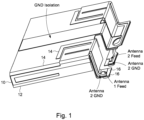
- Fig. 1 shows an example of an antenna 10 for a wireless device.
- the antenna 10 for wireless communication comprises a flexible substrate 12, which forms a cavity structure.
- the antenna 10 comprises one or more conductor lines 14 implemented on the substrate 12.
- the antenna 10 further comprises one or more antenna connectors 16, which are coupled to the one or more conductor lines 14, and which are configured to connect to connector pads of a printed circuit board.
- the conductor lines 14 are configured to form multiple antenna elements (one in the front and one in the back).
- the first antenna element "Antenna 1" has its ground connector in the very front with its "Antenna 1 feed" next to it.
- the second antenna element "Antenna 2" has its ground connector "Antenna 2 GND” behind the gap in the substrate 12 next to the connector of "Antenna 1" and the feed of "Antenna 2" is next to "Antenna 2 GND” further to the back.
- the substrate 12 maybe a foil or any other flexible insulator material, which can serve as base substrate for the conductor lines 14.
- the substrate 12 material may be flexible to an extent that allows the antenna 10 to be clipped on an insulator base structure or a printed circuit board as will be laid out in more detail in the sequel.
- the cavity structure enables the antenna 10 to be clipped on, to be put over, or to cover an insulator base, which sets or defines a distance between the antenna and circuitry underneath to reduce coupling.
- the antenna connectors 16 in Fig. 1 are connectors, which enable an electrical connection or coupling to corresponding connector pads on a printed circuit board through a clamp- or clipped connection, e.g. just by touching the connector pads on the printed circuit board. Therefore, the antenna can be mounted without the use of antenna cables.
- Fig. 1 further shows an optional ground isolation in the center of the substrate structure.
- the flexible substrate 12 is configured to form a cover structure for a wireless communication module, as will be further detailed subsequently.
- the conductor lines 14 can be configured to form a planar inverted-F antenna as shown in Fig. 1 . In other examples, the conductor lines 14 may be configured to form a micro strip antenna.
- Wireless modules are, for example, made in a M.2 (also referred to as next generation form factor (NGFF)) or other module configuration. Due to a demand for a small form factor in embedded products, the modules may use a variety of miniature antenna connectors. In conventional concepts there may be a need for a cable to connect the external antennas to these small miniature antenna connectors.
- M.2 also referred to as next generation form factor (NGFF)
- NGFF next generation form factor
- Fig. 2 shows a wireless communication module with antenna cables and antennas, and a wireless communication module with a printed antenna.
- Fig. 2 shows an M.2 wireless module with antenna miniature connectors at the top left and two antennas at the top right. In between, antenna cables are shown, which are used to connect the wireless module to the antennas using the antenna cables.
- Fig. 2 shows a wireless communication module with a printed circuit board, which has a printed antenna.
- the antenna cables have been a challenge from multiple aspects:
- modules use printed antennas or integrated antennas as the one shown at the bottom of Fig. 2 , which may eliminate the need for cables.
- the antenna used in module of Fig. 2 is a microstrip antenna that is constructed using a microstrip transmission line on an extension of the module PCB (printed circuit board).
- Such a method of integrating an antenna as part of the module may be limited to a single antenna due to size limitation and space required to incorporate two antennas needed for MIMO (multiple-input-multiple-output) configuration with adequate performance and needed isolation. They are also constrained to single frequency band and compromised performance (i.e., gain flatness, and return loss).
- Examples may use a clip-on concept, which may eliminate the need for antenna cables while achieving adequate performance in MIMO configurations with very stable and secure attachment to the module using the same screw that holds the module to the motherboard.
- the antennas 10 may be constructed using a rigid plastic base as support structure and a semi-rigid or flexible PCB as substrate 12 that incorporates and integrates the antenna and antenna connectors. This antenna 10 assembly may enhance stability against any shock and vibration. Examples may eliminate the difficulty in selecting the right antenna cable/connectors and provide a very compact and stable MIMO. Examples may allow cost savings by replacing cable and two external antennas with one plastic base and a semi-rigid PCB antenna 10.
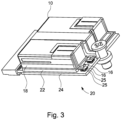
- Fig. 3 shows an example of a mounted wireless communication module 20.
- the wireless communication module 20 comprises an antenna module with an insulator base support structure 18 and an antenna 10 according to Fig. 1 .
- the wireless communication module 20 further comprises communication circuitry 22 on a printed circuit board 24, which is covered by the antenna module 10, 18.
- the communication circuitry 22 may comprise a chip or a semiconductor device with an implementation of a wireless modem for a respective communication standard, e.g. WiFi, BT, LTE, etc.
- the communication circuitry 22 is configured for wireless communication according to IEEE (Institute of Electrical and Electronics Engineers) 802.11.
- the antenna module, the insulator support structure 18 and the antenna 10 is clipped on the printed circuit board 24, covering the communication circuitry 22.
- the communication circuitry 22 resides in or under the cavity structure formed by the antenna 10 and the support structure 18.
- the printed circuit board 24 comprises antenna connector pads 25 and the one or more antenna connectors 16 of the antenna 10 are directly connected (without cables or intermediate components) to the antenna connector pads 25.
- Examples may use one or more PIFA (Planar Inverted-F Antenna) type antennas manufactured on a flexible or semi-rigid PCB 12 (e.g. a foil carrier) and attached to an insulator-based support 18.
- PIFA Planar Inverted-F Antenna
- a PIFA type antenna may be favorized as it can fit in smaller size with improved performance in terms of efficiency, gain and better SAR (specific absorption rate), however, in the future microstrip type antennas could also be a viable solution.
- the wireless communication module 20 may be configured as a M.2 module.
- FIG. 3 An example of a complete antenna configuration attached to a wireless M.2 module concept is shown in Fig. 3 .
- the antenna module 10, 18 and the printed circuit board 24 comprise a common attachment or mounting option.
- the common attachment or mounting option is implemented as a common recess for a screw.
- the antenna and module assembly are shown in Figs. 6 and 7 .
- the antenna assembly begins with putting the insulator base 18 on the module ( Fig. 6 at the bottom) and next wrapping and attaching the flexible semi-rigid antenna 10 on top of the insulator base 18 ( Fig. 7 ).
- the screw 30 will secure the M.2 module 20 and antenna assembly to a motherboard ( Fig. 7 ).
- the mounting of the antenna 10 ( Fig. 1 ) onto the insulator base 18 may be done at an antenna manufacturing site and an end user just puts the whole antenna system 10, 18 (e.g. components 10 and 18 of Fig. 5 are attached together in one piece) on the module 22, 24 and clip-on the antenna connectors 25 and screws the entire module 20 onto the mother board 26.
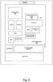
- Fig. 8 illustrates an example of a computing device 700 in accordance with one implementation of the invention.
- the computing device 700 houses a board 702, 26.
- the board 702 may include a number of components, including but not limited to a processor 704 and at least one communication chip 706, 20.
- the processor 704 is physically and electrically coupled to the board 702.
- the at least one communication chip 706, 20 is also physically and electrically coupled to the board 702, 26.
- communication chip 706 may be comprised in a wireless communication module 20, which mounted onto a motherboard 26 using an M.2 socket and a screw.
- computing device 700 may include other components that may or may not be physically and electrically coupled to the board 702.
- volatile memory e.g., DRAM
- non-volatile memory e.g., ROM
- flash memory e.g., a graphics processor, a digital signal processor, a crypto processor, a chipset, an antenna, a display, a touchscreen display, a touchscreen controller, a battery, an audio codec, a video codec, a power amplifier, a global positioning system (GPS) device, a compass, an accelerometer, a gyroscope, a speaker, a camera, and a mass storage device (such as hard disk drive, compact disk (CD), digital versatile disk (DVD), and so forth).
- volatile memory e.g., DRAM
- non-volatile memory e.g., ROM
- flash memory e.g., a graphics processor, a digital signal processor, a crypto processor, a chipset, an antenna, a display, a touchscreen display, a touchscreen controller, a battery, an audio codec, a video codec,
- the communication chip 706, 20 enables wireless communications for the transfer of data to and from the computing device 700.
- wireless and its derivatives may be used to describe circuits, devices, systems, methods, techniques, communications channels, etc., that may communicate data through the use of modulated electromagnetic radiation through a non- solid medium. The term does not imply that the associated devices do not contain any wires, although in some embodiments they might not.
- the communication chip 706, 20 may implement any of a number of wireless standards or protocols, including but not limited to Wi-Fi (IEEE 802.11 family), WiMAX (IEEE 802.16 family), IEEE 802.20, long term evolution (LTE), Ev-DO, HSPA+, HSDPA+, HSUPA+, EDGE, GSM, GPRS, CDMA, TDMA, DECT, Bluetooth, derivatives thereof, as well as any other wireless protocols that are designated as 3G, 4G, 5G, and beyond.
- the computing device 700 may include a plurality of communication chips 706.
- a first communication chip 706 may be dedicated to shorter range wireless communications such as Wi-Fi and Bluetooth and a second communication chip 706 may be dedicated to longer range wireless communications such as GPS, EDGE, GPRS, CDMA, WiMAX, LTE, Ev-DO, and others.
- the processor 704 of the computing device 700 includes an integrated circuit die packaged within the processor 704.
- the integrated circuit die of the processor includes one or more devices that are assembled in an ePLB or eWLB based P0P package that that includes a mold layer directly contacting a substrate, in accordance with implementations of the invention.
- the term "processor" may refer to any device or portion of a device that processes electronic data from registers and/or memory to transform that electronic data into other electronic data that may be stored in registers and/or memory.
- the communication chip 706 also includes an integrated circuit die packaged within the communication chip 706.
- the integrated circuit die of the communication chip includes one or more devices that are assembled in an ePLB or eWLB based P0P package that that includes a mold layer directly contacting a substrate, in accordance with implementations of the invention.
- Examples may further be or relate to a (computer) program including a program code to execute one or more of the above methods when the program is executed on a computer, processor or other programmable hardware component.
- steps, operations or processes of different ones of the methods described above may also be executed by programmed computers, processors or other programmable hardware components.
- Examples may also cover program storage devices, such as digital data storage media, which are machine-, processor- or computer-readable and encode and/or contain machine-executable, processor-executable or computer-executable programs and instructions.
- Program storage devices may include or be digital storage devices, magnetic storage media such as magnetic disks and magnetic tapes, hard disk drives, or optically readable digital data storage media, for example.
- Other examples may also include computers, processors, control units, (field) programmable logic arrays ((F)PLAs), (field) programmable gate arrays ((F)PGAs), graphics processor units (GPU), application-specific integrated circuits (ASICs), integrated circuits (ICs) or system-on-a-chip (SoCs) systems programmed to execute the steps of the methods described above.
- FPLAs field programmable logic arrays
- F field) programmable gate arrays
- GPU graphics processor units
- ASICs application-specific integrated circuits
- ICs integrated circuits
- SoCs system-on-a-chip
- aspects described in relation to a device or system should also be understood as a description of the corresponding method.
- a block, device or functional aspect of the device or system may correspond to a feature, such as a method step, of the corresponding method.
- aspects described in relation to a method shall also be understood as a description of a corresponding block, a corresponding element, a property or a functional feature of a corresponding device or a corresponding system.
- An example (e.g., example 1) relates to an antenna (10) for a wireless device, the antenna (10) comprising a flexible substrate (12), which forms a cavity structure; one or more conductor lines (14) implemented on the substrate (12); and one or more antenna connectors (16), which are coupled to the one or more conductor lines (14), and which are configured to connect to connector pads (25) of a printed circuit board (24).
- Another example (e.g., example 2) relates to the antenna (10) as previously described, wherein the flexible substrate (12) is configured to form a cover structure for a wireless communication module (20).
- Another example (e.g., example 3) relates to the antenna (10) as previously described, wherein the conductor lines (14) are configured to form multiple antenna elements.
- Another example (e.g., example 4) relates to the antenna (10) as previously described, wherein the conductor lines (14) are configured to form a planar inverted-F antenna.
- Another example (e.g., example 5) relates to the antenna (10) as previously described, wherein the conductor lines (14) are configured to form a micro strip antenna.
- Another example (e.g., example 6) relates to antenna module, comprising an insulator base support structure (18) and an antenna (10) as previously described.
- Another example is a wireless communication module (20) comprising the antenna module as previously described.
- Another example is the wireless communication module (20) as previously described, further comprising communication circuitry (22) on a printed circuit board (24), which is covered by the antenna module.
- Another example is the wireless communication module (20) as previously described, wherein the antenna module is clipped on the printed circuit board (24).
- Another example is the wireless communication module (20) as previously described, wherein the printed circuit board (24) comprises antenna connector pads (25) and wherein the one or more antenna connectors (16) of the antenna (10) are directly connected to the antenna connector pads (25.
- Another example is the wireless communication module (20) as previously described, wherein the antenna module and the printed circuit board (24) comprise a common attachment option.
- Another example is the wireless communication module (20) as previously described, wherein the communication circuitry (22) is configured for wireless communication according to IEEE 802.11.
- Another example is the wireless communication module (20) as previously described, being configured as a M.2 module.
- Another example is a main board (26) for a computer comprising the wireless communication module (20) as previously described.
- Another example is the main board (26) as previously described, wherein the wireless communication module (20) is attached to the main board (26) with an M.2 socket and one additional screw.
- Another example is a computer device or system with a main board as previously described.
- Another example is a manufacturing method comprising mounting an antenna (10) as previously described on an insulator base support structure (18) to obtain an antenna module; mounting the antenna module onto a PCB (24) with a communication circuitry (22) to obtain a wireless communication module (20).
- Another example is the manufacturing method as previously described further comprising mounting the wireless communication module (20) onto a main- or mother board (26) of a computer device or system.
Landscapes
- Engineering & Computer Science (AREA)
- Microelectronics & Electronic Packaging (AREA)
- Support Of Aerials (AREA)
Abstract
Description
- Examples relate to an antenna, an antenna module, a wireless communication module, a main board and a computer device, more particularly, but not exclusively, to an antenna concept for a wireless communication module.
- Some conventional systems provide wireless communication services using wireless standards such as Wireless Fidelity (WiFi), Bluetooth (BT), and Long Term Evolution (LTE). In such cases wireless communication modules may be used to provide wireless services to other components of the system and to enable data wireless data exchange for computer devices. Typically, such wireless communication modules comprise high frequency components such as mixers, filters, low noise amplifiers, power amplifiers, diplexers, duplexers, antennas, antenna cables, etc.
- Some examples of apparatuses and/or methods will be described in the following by way of example only, and with reference to the accompanying figures, in which
-
Fig. 1 shows an example of an antenna; -
Fig. 2 shows a wireless communication module with antenna cables and antennas, and a wireless communication module with a printed antenna; -
Fig. 3 shows an example of a mounted wireless communication module; -
Fig. 4 shows mounting of an M.2 socket for a wireless communication module on a motherboard; -
Fig. 5 shows examples of a wireless communication chip on a printed circuit board, an insulator base support covering the chip and an antenna adapted to the insulator base; -
Fig. 6 further illustrates the mounting of a wireless communication module in an example; -
Fig. 7 illustrates the mounting of a wireless communication module on a main board using a single screw in an example; and -
Fig. 8 shows an example of a computing device. - Some examples are now described in more detail with reference to the enclosed figures. However, other possible examples are not limited to the features of these embodiments described in detail. Other examples may include modifications of the features as well as equivalents and alternatives to the features. Furthermore, the terminology used herein to describe certain examples should not be restrictive of further possible examples.
- Throughout the description of the figures same or similar reference numerals refer to same or similar elements and/or features, which may be identical or implemented in a modified form while providing the same or a similar function. The thickness of lines, layers and/or areas in the figures may also be exaggerated for clarification.
- When two elements A and B are combined using an "or", this is to be understood as disclosing all possible combinations, i.e. only A, only B as well as A and B, unless expressly defined otherwise in the individual case. As an alternative wording for the same combinations, "at least one of A and B" or "A and/or B" may be used. This applies equivalently to combinations of more than two elements.
- If a singular form, such as "a", "an" and "the" is used and the use of only a single element is not defined as mandatory either explicitly or implicitly, further examples may also use several elements to implement the same function. If a function is described below as implemented using multiple elements, further examples may implement the same function using a single element or a single processing entity. It is further understood that the terms "include", "including", "comprise" and/or "comprising", when used, describe the presence of the specified features, integers, steps, operations, processes, elements, components and/or a group thereof, but do not exclude the presence or addition of one or more other features, integers, steps, operations, processes, elements, components and/or a group thereof.
-
Fig. 1 shows an example of anantenna 10 for a wireless device. Theantenna 10 for wireless communication comprises aflexible substrate 12, which forms a cavity structure. Theantenna 10 comprises one ormore conductor lines 14 implemented on thesubstrate 12. Theantenna 10 further comprises one ormore antenna connectors 16, which are coupled to the one ormore conductor lines 14, and which are configured to connect to connector pads of a printed circuit board. In the example shown inFig. 1 theconductor lines 14 are configured to form multiple antenna elements (one in the front and one in the back). The first antenna element "Antenna 1" has its ground connector in the very front with its "Antenna 1 feed" next to it. The second antenna element "Antenna 2" has its ground connector "Antenna 2 GND" behind the gap in thesubstrate 12 next to the connector of "Antenna 1" and the feed of "Antenna 2" is next to "Antenna 2 GND" further to the back. - The
substrate 12 maybe a foil or any other flexible insulator material, which can serve as base substrate for theconductor lines 14. Thesubstrate 12 material may be flexible to an extent that allows theantenna 10 to be clipped on an insulator base structure or a printed circuit board as will be laid out in more detail in the sequel. - The cavity structure enables the
antenna 10 to be clipped on, to be put over, or to cover an insulator base, which sets or defines a distance between the antenna and circuitry underneath to reduce coupling. - The
antenna connectors 16 inFig. 1 are connectors, which enable an electrical connection or coupling to corresponding connector pads on a printed circuit board through a clamp- or clipped connection, e.g. just by touching the connector pads on the printed circuit board. Therefore, the antenna can be mounted without the use of antenna cables. -
Fig. 1 further shows an optional ground isolation in the center of the substrate structure. As further shown inFig. 1 theflexible substrate 12 is configured to form a cover structure for a wireless communication module, as will be further detailed subsequently. In examples, there are multiple options for antenna types formed by theconductor lines 14. Theconductor lines 14 can be configured to form a planar inverted-F antenna as shown inFig. 1 . In other examples, theconductor lines 14 may be configured to form a micro strip antenna. - Wireless modules (e.g. using WiFi, BT, LTE) are, for example, made in a M.2 (also referred to as next generation form factor (NGFF)) or other module configuration. Due to a demand for a small form factor in embedded products, the modules may use a variety of miniature antenna connectors. In conventional concepts there may be a need for a cable to connect the external antennas to these small miniature antenna connectors.
-
Fig. 2 shows a wireless communication module with antenna cables and antennas, and a wireless communication module with a printed antenna.Fig. 2 shows an M.2 wireless module with antenna miniature connectors at the top left and two antennas at the top right. In between, antenna cables are shown, which are used to connect the wireless module to the antennas using the antenna cables. At the bottom,Fig. 2 shows a wireless communication module with a printed circuit board, which has a printed antenna. - The antenna cables have been a challenge from multiple aspects:
- 1) Mechanical stability during shock and vibration, which is a major concern for applications such as automotive and industrial.
- 2) Losses associated with the cable decrease the output power of the wireless module and therefore the range and coverage.
- 3) Customer confusion and difficulty in finding the right antenna cable, which has been one of the deterrents in WiFi IOT (internet of things) eco system development. There are many different types, standards and names for the miniature antenna connector such as U.FL, or MHF4 or IPEX.
- Selecting the right kind of cable has been a challenge for a lot of users.
- Some modules use printed antennas or integrated antennas as the one shown at the bottom of
Fig. 2 , which may eliminate the need for cables. The antenna used in module ofFig. 2 is a microstrip antenna that is constructed using a microstrip transmission line on an extension of the module PCB (printed circuit board). Such a method of integrating an antenna as part of the module may be limited to a single antenna due to size limitation and space required to incorporate two antennas needed for MIMO (multiple-input-multiple-output) configuration with adequate performance and needed isolation. They are also constrained to single frequency band and compromised performance (i.e., gain flatness, and return loss). - Examples may use a clip-on concept, which may eliminate the need for antenna cables while achieving adequate performance in MIMO configurations with very stable and secure attachment to the module using the same screw that holds the module to the motherboard. The
antennas 10 may be constructed using a rigid plastic base as support structure and a semi-rigid or flexible PCB assubstrate 12 that incorporates and integrates the antenna and antenna connectors. Thisantenna 10 assembly may enhance stability against any shock and vibration. Examples may eliminate the difficulty in selecting the right antenna cable/connectors and provide a very compact and stable MIMO. Examples may allow cost savings by replacing cable and two external antennas with one plastic base and asemi-rigid PCB antenna 10. -
Fig. 3 shows an example of a mountedwireless communication module 20. Thewireless communication module 20 comprises an antenna module with an insulatorbase support structure 18 and anantenna 10 according toFig. 1 . Thewireless communication module 20 further comprisescommunication circuitry 22 on a printedcircuit board 24, which is covered by theantenna module communication circuitry 22 may comprise a chip or a semiconductor device with an implementation of a wireless modem for a respective communication standard, e.g. WiFi, BT, LTE, etc. For example, thecommunication circuitry 22 is configured for wireless communication according to IEEE (Institute of Electrical and Electronics Engineers) 802.11. - As can be seen from
Fig. 3 the antenna module, theinsulator support structure 18 and theantenna 10, is clipped on the printedcircuit board 24, covering thecommunication circuitry 22. Thecommunication circuitry 22 resides in or under the cavity structure formed by theantenna 10 and thesupport structure 18. - The printed
circuit board 24 comprisesantenna connector pads 25 and the one ormore antenna connectors 16 of theantenna 10 are directly connected (without cables or intermediate components) to theantenna connector pads 25. - Examples may use one or more PIFA (Planar Inverted-F Antenna) type antennas manufactured on a flexible or semi-rigid PCB 12 (e.g. a foil carrier) and attached to an insulator-based
support 18. For example, a PIFA type antenna may be favorized as it can fit in smaller size with improved performance in terms of efficiency, gain and better SAR (specific absorption rate), however, in the future microstrip type antennas could also be a viable solution. In examples, thewireless communication module 20 may be configured as a M.2 module. - An example of a complete antenna configuration attached to a wireless M.2 module concept is shown in
Fig. 3 . As further illustrated byFig. 3 theantenna module circuit board 24 comprise a common attachment or mounting option. The common attachment or mounting option is implemented as a common recess for a screw. -
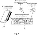
Fig. 4 shows mounting of an M.2 socket for a wireless communication module on amotherboard 26 in an example.Fig. 4 illustrates an M.2socket 28 mounted on themotherboard 26. - A
screw 30 is used to secure the module and antenna assembly. A screw nut 32 is mounted on themotherboard 26. Another example is a main board ormotherboard 26 for a computer comprising thewireless communication module 20. For example, thewireless communication module 20 is attached to themain board 26 with an M.2socket 28 and oneadditional screw 30. -
Fig. 5 shows examples of awireless communication chip 22 on a printedcircuit board 24, aninsulator base support 18, which is configured to cover thechip 22 and anantenna 10 adapted to theinsulator base 18. InFig. 5 the respective components are shown separately to illustrate the mounting process. Thechip 22 on thePCB 24 is covered with theinsulator base 18. Theinsulator base 18 ensures theantenna 10, which gets mounted on top of theinsulator base 18, has a certain distance from thechip 22 to avoid strong electromagnetic coupling with thechip 22.Fig. 6 further illustrate the mounting of awireless communication module 20 in an example.Fig. 7 illustrates the mounting of awireless communication module 20 on a main board using a single screw in an example. -
Fig. 5 shows thecomponents Figs. 6 and7 . The M.2socket 28 and screw nut 32 - The antenna and module assembly are shown in
Figs. 6 and7 . Once the M.2module 20 is inserted into thesocket 28 and secured the antenna assembly starts (Fig. 6 at the top). The antenna assembly begins with putting theinsulator base 18 on the module (Fig. 6 at the bottom) and next wrapping and attaching the flexiblesemi-rigid antenna 10 on top of the insulator base 18 (Fig. 7 ). Finally, thescrew 30 will secure the M.2module 20 and antenna assembly to a motherboard (Fig. 7 ). For example, the mounting of the antenna 10 (Fig. 1 ) onto theinsulator base 18 may be done at an antenna manufacturing site and an end user just puts thewhole antenna system 10, 18 (e.g. components Fig. 5 are attached together in one piece) on themodule antenna connectors 25 and screws theentire module 20 onto themother board 26. -
Fig. 8 illustrates an example of a computing device 700 in accordance with one implementation of the invention. The computing device 700 houses aboard board 702 may include a number of components, including but not limited to aprocessor 704 and at least onecommunication chip processor 704 is physically and electrically coupled to theboard 702. In some implementations the at least onecommunication chip board communication chip 706 may be comprised in awireless communication module 20, which mounted onto amotherboard 26 using an M.2 socket and a screw. Depending on its applications, computing device 700 may include other components that may or may not be physically and electrically coupled to theboard 702. These other components include, but are not limited to, volatile memory (e.g., DRAM), non-volatile memory (e.g., ROM), flash memory, a graphics processor, a digital signal processor, a crypto processor, a chipset, an antenna, a display, a touchscreen display, a touchscreen controller, a battery, an audio codec, a video codec, a power amplifier, a global positioning system (GPS) device, a compass, an accelerometer, a gyroscope, a speaker, a camera, and a mass storage device (such as hard disk drive, compact disk (CD), digital versatile disk (DVD), and so forth). - The
communication chip communication chip communication chips 706. For instance, afirst communication chip 706 may be dedicated to shorter range wireless communications such as Wi-Fi and Bluetooth and asecond communication chip 706 may be dedicated to longer range wireless communications such as GPS, EDGE, GPRS, CDMA, WiMAX, LTE, Ev-DO, and others. - The
processor 704 of the computing device 700 includes an integrated circuit die packaged within theprocessor 704. In some implementations of the invention, the integrated circuit die of the processor includes one or more devices that are assembled in an ePLB or eWLB based P0P package that that includes a mold layer directly contacting a substrate, in accordance with implementations of the invention. The term "processor" may refer to any device or portion of a device that processes electronic data from registers and/or memory to transform that electronic data into other electronic data that may be stored in registers and/or memory. Thecommunication chip 706 also includes an integrated circuit die packaged within thecommunication chip 706. In accordance with another implementation of the invention, the integrated circuit die of the communication chip includes one or more devices that are assembled in an ePLB or eWLB based P0P package that that includes a mold layer directly contacting a substrate, in accordance with implementations of the invention. - The aspects and features described in relation to a particular one of the previous examples may also be combined with one or more of the further examples to replace an identical or similar feature of that further example or to additionally introduce the features into the further example.
- Examples may further be or relate to a (computer) program including a program code to execute one or more of the above methods when the program is executed on a computer, processor or other programmable hardware component. Thus, steps, operations or processes of different ones of the methods described above may also be executed by programmed computers, processors or other programmable hardware components. Examples may also cover program storage devices, such as digital data storage media, which are machine-, processor- or computer-readable and encode and/or contain machine-executable, processor-executable or computer-executable programs and instructions. Program storage devices may include or be digital storage devices, magnetic storage media such as magnetic disks and magnetic tapes, hard disk drives, or optically readable digital data storage media, for example. Other examples may also include computers, processors, control units, (field) programmable logic arrays ((F)PLAs), (field) programmable gate arrays ((F)PGAs), graphics processor units (GPU), application-specific integrated circuits (ASICs), integrated circuits (ICs) or system-on-a-chip (SoCs) systems programmed to execute the steps of the methods described above.
- It is further understood that the disclosure of several steps, processes, operations or functions disclosed in the description or claims shall not be construed to imply that these operations are necessarily dependent on the order described, unless explicitly stated in the individual case or necessary for technical reasons. Therefore, the previous description does not limit the execution of several steps or functions to a certain order. Furthermore, in further examples, a single step, function, process or operation may include and/or be broken up into several sub-steps, -functions, -processes or -operations.
- If some aspects have been described in relation to a device or system, these aspects should also be understood as a description of the corresponding method. For example, a block, device or functional aspect of the device or system may correspond to a feature, such as a method step, of the corresponding method. Accordingly, aspects described in relation to a method shall also be understood as a description of a corresponding block, a corresponding element, a property or a functional feature of a corresponding device or a corresponding system.
- An example (e.g., example 1) relates to an antenna (10) for a wireless device, the antenna (10) comprising a flexible substrate (12), which forms a cavity structure; one or more conductor lines (14) implemented on the substrate (12); and one or more antenna connectors (16), which are coupled to the one or more conductor lines (14), and which are configured to connect to connector pads (25) of a printed circuit board (24).
- Another example (e.g., example 2) relates to the antenna (10) as previously described, wherein the flexible substrate (12) is configured to form a cover structure for a wireless communication module (20).
- Another example (e.g., example 3) relates to the antenna (10) as previously described, wherein the conductor lines (14) are configured to form multiple antenna elements.
- Another example (e.g., example 4) relates to the antenna (10) as previously described, wherein the conductor lines (14) are configured to form a planar inverted-F antenna.
- Another example (e.g., example 5) relates to the antenna (10) as previously described, wherein the conductor lines (14) are configured to form a micro strip antenna.
- Another example (e.g., example 6) relates to antenna module, comprising an insulator base support structure (18) and an antenna (10) as previously described.
- Another example (e.g., example 7) is a wireless communication module (20) comprising the antenna module as previously described.
- Another example (e.g., example 8) is the wireless communication module (20) as previously described, further comprising communication circuitry (22) on a printed circuit board (24), which is covered by the antenna module.
- Another example (e.g., example 9) is the wireless communication module (20) as previously described, wherein the antenna module is clipped on the printed circuit board (24).
- Another example (e.g., example 10) is the wireless communication module (20) as previously described, wherein the printed circuit board (24) comprises antenna connector pads (25) and wherein the one or more antenna connectors (16) of the antenna (10) are directly connected to the antenna connector pads (25.
- Another example (e.g., example 11) is the wireless communication module (20) as previously described, wherein the antenna module and the printed circuit board (24) comprise a common attachment option.
- Another example (e.g., example 12) is the wireless communication module (20) as previously described, wherein the communication circuitry (22) is configured for wireless communication according to IEEE 802.11.
- Another example (e.g., example 13) is the wireless communication module (20) as previously described, being configured as a M.2 module.
- Another example (e.g., example 14) is a main board (26) for a computer comprising the wireless communication module (20) as previously described.
- Another example (e.g., example 15) is the main board (26) as previously described, wherein the wireless communication module (20) is attached to the main board (26) with an M.2 socket and one additional screw.
- Another example (e.g., example 16) is a computer device or system with a main board as previously described.
- Another example (e.g., example 17) is a manufacturing method comprising mounting an antenna (10) as previously described on an insulator base support structure (18) to obtain an antenna module; mounting the antenna module onto a PCB (24) with a communication circuitry (22) to obtain a wireless communication module (20).
- Another example (e.g., example 18) is the manufacturing method as previously described further comprising mounting the wireless communication module (20) onto a main- or mother board (26) of a computer device or system.
- The following claims are hereby incorporated in the detailed description, wherein each claim may stand on its own as a separate example. It should also be noted that although in the claims a dependent claim refers to a particular combination with one or more other claims, other examples may also include a combination of the dependent claim with the subject matter of any other dependent or independent claim. Such combinations are hereby explicitly proposed, unless it is stated in the individual case that a particular combination is not intended. Furthermore, features of a claim should also be included for any other independent claim, even if that claim is not directly defined as dependent on that other independent claim.
Claims (15)
- An antenna (10) for a wireless device, the antenna (10) comprising a flexible substrate (12), which forms a cavity structure;
one or more conductor lines (14) implemented on the substrate (12);
one or more antenna connectors (16), which are coupled to the one or more conductor lines (14), and which are configured to connect to connector pads (25) of a printed circuit board (24). - The antenna (10) of claim 1, wherein the flexible substrate (12) is configured to form a cover structure for a wireless communication module (20).
- The antenna (10) of one of the claims 1 or 2, wherein the conductor lines (14) are configured to form multiple antenna elements.
- The antenna (10) of one of the claims 1 to 3, wherein the conductor lines (14) are configured to form a planar inverted-F antenna.
- The antenna (10) of one of the claims 1 to 3, wherein the conductor lines (14) are configured to form a micro strip antenna.
- An antenna module, comprising an insulator base support structure (18) and an antenna (10) according to any one of claims 1 to 5.
- A wireless communication module (20) comprising the antenna module of claim 6.
- The wireless communication module (20) of claim 7, further comprising communication circuitry (22) on a printed circuit board (24), which is covered by the antenna module.
- The wireless communication module (20) of claim 8, wherein the antenna module is clipped on the printed circuit board (24).
- The wireless communication module (20) of one of the claims 8 or 9, wherein the printed circuit board (24) comprises antenna connector pads (25) and wherein the one or more antenna connectors (16) of the antenna (10) are directly connected to the antenna connector pads (25.
- The wireless communication module (20) of one of the claims 8 to 10, wherein the antenna module and the printed circuit board (24) comprise a common attachment option.
- The wireless communication module (20) of one of the claims 8 to 11, wherein the communication circuitry (22) is configured for wireless communication according to IEEE 802.11.
- The wireless communication module (20) of one of the claims 8 to 12, being configured as a M.2 module.
- A main board (26) for a computer comprising the wireless communication module (20) of one of the claims 8 to 13.
- The main board (26) of claim 15, wherein the wireless communication module (20) is attached to the main board (26) with an M.2 socket and one additional screw.
Priority Applications (1)
| Application Number | Priority Date | Filing Date | Title |
|---|---|---|---|
| EP21216715.9A EP4203178A1 (en) | 2021-12-22 | 2021-12-22 | An antenna, a wireless communication module, a main board and a computer device |
Applications Claiming Priority (1)
| Application Number | Priority Date | Filing Date | Title |
|---|---|---|---|
| EP21216715.9A EP4203178A1 (en) | 2021-12-22 | 2021-12-22 | An antenna, a wireless communication module, a main board and a computer device |
Publications (1)
| Publication Number | Publication Date |
|---|---|
| EP4203178A1 true EP4203178A1 (en) | 2023-06-28 |
Family
ID=79018772
Family Applications (1)
| Application Number | Title | Priority Date | Filing Date |
|---|---|---|---|
| EP21216715.9A Pending EP4203178A1 (en) | 2021-12-22 | 2021-12-22 | An antenna, a wireless communication module, a main board and a computer device |
Country Status (1)
| Country | Link |
|---|---|
| EP (1) | EP4203178A1 (en) |
Citations (5)
| Publication number | Priority date | Publication date | Assignee | Title |
|---|---|---|---|---|
| US20040196190A1 (en) * | 2003-04-02 | 2004-10-07 | Mendolia Gregory S. | Method for fabrication of miniature lightweight antennas |
| US20070262909A1 (en) * | 2006-05-04 | 2007-11-15 | Samsung Electro-Mechanics Co., Ltd. | Inverted-F antenna and mobile communication terminal using the same |
| KR20100000940U (en) * | 2008-07-18 | 2010-01-27 | 주식회사 힝스 | Multifunctional Gender with Antenna |
| US20140159990A1 (en) * | 2012-12-11 | 2014-06-12 | Opticon Sensors Europe B.V. | Antenna mounted on a circuit board |
| US20200280120A1 (en) * | 2019-03-01 | 2020-09-03 | Microsoft Technology Licensing, Llc | High Frequency Antenna Integration in Electronic Devices |
-
2021
- 2021-12-22 EP EP21216715.9A patent/EP4203178A1/en active Pending
Patent Citations (5)
| Publication number | Priority date | Publication date | Assignee | Title |
|---|---|---|---|---|
| US20040196190A1 (en) * | 2003-04-02 | 2004-10-07 | Mendolia Gregory S. | Method for fabrication of miniature lightweight antennas |
| US20070262909A1 (en) * | 2006-05-04 | 2007-11-15 | Samsung Electro-Mechanics Co., Ltd. | Inverted-F antenna and mobile communication terminal using the same |
| KR20100000940U (en) * | 2008-07-18 | 2010-01-27 | 주식회사 힝스 | Multifunctional Gender with Antenna |
| US20140159990A1 (en) * | 2012-12-11 | 2014-06-12 | Opticon Sensors Europe B.V. | Antenna mounted on a circuit board |
| US20200280120A1 (en) * | 2019-03-01 | 2020-09-03 | Microsoft Technology Licensing, Llc | High Frequency Antenna Integration in Electronic Devices |
Similar Documents
| Publication | Publication Date | Title |
|---|---|---|
| US11430751B2 (en) | Microelectronic devices designed with 3D stacked ultra thin package modules for high frequency communications | |
| US20220246554A1 (en) | Microelectronic devices designed with compound semiconductor devices and integrated on an inter die fabric | |
| US11387200B2 (en) | Microelectronic devices with high frequency communication modules having compound semiconductor devices integrated on a package fabric | |
| US10886606B2 (en) | Microelectronic devices designed with flexible package substrates with distributed stacked antennas for high frequency communication systems | |
| US20200236205A1 (en) | Microelectronic devices designed with integrated antenna on a substrate | |
| US10056182B2 (en) | Surface-mount inductor structures for forming one or more inductors with substrate traces | |
| CN111886755A (en) | Antenna module and communication device | |
| US9237659B2 (en) | BGA structure using CTF balls in high stress regions | |
| US11876304B2 (en) | Multiband patch antenna | |
| US20180090467A1 (en) | Package with thermal coupling | |
| US9960104B2 (en) | Integrated package design with wire leads for package-on-package product | |
| US20210287993A1 (en) | Microelectronic structures having notched microelectronic substrates | |
| US10637147B2 (en) | Wideband antennas | |
| CN116581540A (en) | Combining Antennas and Electronics | |
| CN109716510B (en) | Floating package stiffener | |
| EP4203178A1 (en) | An antenna, a wireless communication module, a main board and a computer device | |
| US9491881B2 (en) | Microelectronic socket comprising a substrate and an insulative insert mated with openings in the substrate | |
| US20170372989A1 (en) | Exposed side-wall and lga assembly | |
| TWI622226B (en) | Grounded excitation antenna | |
| US20210305118A1 (en) | Heat spreader edge standoffs for managing bondline thickness in microelectronic packages | |
| US11251111B2 (en) | Leadframe in packages of integrated circuits | |
| CN120917533A (en) | Three-dimensional (3D) inductor with double sided bond wires | |
| US20250293111A1 (en) | Lid through interposer of semiconductor package for thermal management | |
| US20190348766A1 (en) | Slot antenna on a printed circuit board (pcb) | |
| WO2019066922A1 (en) | Package on package assembly |
Legal Events
| Date | Code | Title | Description |
|---|---|---|---|
| PUAI | Public reference made under article 153(3) epc to a published international application that has entered the european phase |
Free format text: ORIGINAL CODE: 0009012 |
|
| STAA | Information on the status of an ep patent application or granted ep patent |
Free format text: STATUS: THE APPLICATION HAS BEEN PUBLISHED |
|
| AK | Designated contracting states |
Kind code of ref document: A1 Designated state(s): AL AT BE BG CH CY CZ DE DK EE ES FI FR GB GR HR HU IE IS IT LI LT LU LV MC MK MT NL NO PL PT RO RS SE SI SK SM TR |
|
| STAA | Information on the status of an ep patent application or granted ep patent |
Free format text: STATUS: REQUEST FOR EXAMINATION WAS MADE |
|
| 17P | Request for examination filed |
Effective date: 20240102 |
|
| RBV | Designated contracting states (corrected) |
Designated state(s): AL AT BE BG CH CY CZ DE DK EE ES FI FR GB GR HR HU IE IS IT LI LT LU LV MC MK MT NL NO PL PT RO RS SE SI SK SM TR |