CN111886755A - Antenna module and communication device - Google Patents
Antenna module and communication device Download PDFInfo
- Publication number
- CN111886755A CN111886755A CN201980021396.9A CN201980021396A CN111886755A CN 111886755 A CN111886755 A CN 111886755A CN 201980021396 A CN201980021396 A CN 201980021396A CN 111886755 A CN111886755 A CN 111886755A
- Authority
- CN
- China
- Prior art keywords
- antenna
- communication device
- package
- array
- coupled
- Prior art date
- Legal status (The legal status is an assumption and is not a legal conclusion. Google has not performed a legal analysis and makes no representation as to the accuracy of the status listed.)
- Pending
Links
Images


Classifications
-
- H—ELECTRICITY
- H01—ELECTRIC ELEMENTS
- H01Q—ANTENNAS, i.e. RADIO AERIALS
- H01Q9/00—Electrically-short antennas having dimensions not more than twice the operating wavelength and consisting of conductive active radiating elements
- H01Q9/04—Resonant antennas
- H01Q9/0407—Substantially flat resonant element parallel to ground plane, e.g. patch antenna
-
- H—ELECTRICITY
- H01—ELECTRIC ELEMENTS
- H01Q—ANTENNAS, i.e. RADIO AERIALS
- H01Q1/00—Details of, or arrangements associated with, antennas
- H01Q1/08—Means for collapsing antennas or parts thereof
- H01Q1/085—Flexible aerials; Whip aerials with a resilient base
-
- H—ELECTRICITY
- H01—ELECTRIC ELEMENTS
- H01Q—ANTENNAS, i.e. RADIO AERIALS
- H01Q1/00—Details of, or arrangements associated with, antennas
- H01Q1/12—Supports; Mounting means
- H01Q1/22—Supports; Mounting means by structural association with other equipment or articles
- H01Q1/2283—Supports; Mounting means by structural association with other equipment or articles mounted in or on the surface of a semiconductor substrate as a chip-type antenna or integrated with other components into an IC package
-
- H—ELECTRICITY
- H01—ELECTRIC ELEMENTS
- H01Q—ANTENNAS, i.e. RADIO AERIALS
- H01Q1/00—Details of, or arrangements associated with, antennas
- H01Q1/36—Structural form of radiating elements, e.g. cone, spiral, umbrella; Particular materials used therewith
- H01Q1/38—Structural form of radiating elements, e.g. cone, spiral, umbrella; Particular materials used therewith formed by a conductive layer on an insulating support
-
- H—ELECTRICITY
- H01—ELECTRIC ELEMENTS
- H01Q—ANTENNAS, i.e. RADIO AERIALS
- H01Q21/00—Antenna arrays or systems
- H01Q21/06—Arrays of individually energised antenna units similarly polarised and spaced apart
- H01Q21/061—Two dimensional planar arrays
- H01Q21/065—Patch antenna array
-
- H—ELECTRICITY
- H01—ELECTRIC ELEMENTS
- H01Q—ANTENNAS, i.e. RADIO AERIALS
- H01Q3/00—Arrangements for changing or varying the orientation or the shape of the directional pattern of the waves radiated from an antenna or antenna system
- H01Q3/01—Arrangements for changing or varying the orientation or the shape of the directional pattern of the waves radiated from an antenna or antenna system varying the shape of the antenna or antenna system
-
- H—ELECTRICITY
- H01—ELECTRIC ELEMENTS
- H01Q—ANTENNAS, i.e. RADIO AERIALS
- H01Q11/00—Electrically-long antennas having dimensions more than twice the shortest operating wavelength and consisting of conductive active radiating elements
- H01Q11/12—Resonant antennas
- H01Q11/14—Resonant antennas with parts bent, folded, shaped or screened or with phasing impedances, to obtain desired phase relation of radiation from selected sections of the antenna or to obtain desired polarisation effect
Abstract
Disclosed herein are an antenna board, an antenna module, and a communication device. For example, in some embodiments, an antenna module may include: an antenna patch support including a flexible portion; an Integrated Circuit (IC) package coupled to the antenna patch support; and an antenna patch coupled to the antenna patch support. Wherein the antenna patch is a millimeter wave antenna patch, and the IC package and the antenna patch are coupled to opposite faces of the antenna patch support.
Description
Cross Reference to Related Applications
The present application claims the benefit of priority from united states non-provisional patent application No. 16/000,795 entitled "ANTENNA module and communication DEVICE (ANTENNA MODULES and communication DEVICE)" filed on 5.6.2018, which is incorporated herein by reference in its entirety.
Background
Wireless communication devices, such as handheld computing devices and wireless access points, include antennas. The frequency at which communication may occur may depend on the shape and arrangement of the antenna or antenna array, among other factors.
Drawings
The embodiments will be readily understood by the following detailed description in conjunction with of the accompanying drawings. For convenience of description, the same reference numeral denotes the same structural element. In the figures of the drawings, embodiments are shown by way of example, and not by way of limitation, .
Fig. 1 is a side cross-sectional view of an antenna module according to various embodiments.
Fig. 2-4 are side cross-sectional views of exemplary antenna boards according to various embodiments.
Fig. 5 is a top view of an exemplary antenna patch in accordance with various embodiments.
Fig. 6-11 are side cross-sectional views of exemplary antenna boards according to various embodiments.
Fig. 12 and 13 are side cross-sectional views of exemplary antenna patches according to various embodiments.
Fig. 14 is a side cross-sectional view of an Integrated Circuit (IC) package that may be included in an antenna module, in accordance with various embodiments.
Fig. 15A-15C are views of an exemplary antenna module according to various embodiments.
Fig. 16A-16B and 17-18 are side cross-sectional views of exemplary antenna modules according to various embodiments.
Fig. 19 and 20 are bottom views of exemplary antenna patch arrangements in antenna boards according to various embodiments.
Figure 21 is a side cross-sectional view of an exemplary antenna patch arrangement in an antenna board according to various embodiments.
Fig. 22 is a side cross-sectional view of a portion of a communication device including an antenna module, in accordance with various embodiments.
Fig. 23 and 24 are side cross-sectional views of an exemplary assembly including an antenna module and a circuit board according to various embodiments.
Fig. 25A and 25B are various views of an exemplary communication device including an antenna module, in accordance with various embodiments.
Fig. 26A and 26B are various views of an exemplary communication device including an antenna module, in accordance with various embodiments.
Figure 27 is a top view of an exemplary antenna board, in accordance with various embodiments.
Figure 28 is a side cross-sectional view of the antenna plate of figure 27 coupled to an antenna plate mount, in accordance with various embodiments.
Figure 29 is a top view of an exemplary antenna board, in accordance with various embodiments.
Figure 30 is a side cross-sectional view of the antenna plate of figure 29 coupled to an antenna plate mount, in accordance with various embodiments.
Fig. 31A and 31B are top and side cross-sectional views, respectively, of an antenna plate coupled to an antenna plate mount, according to various embodiments.
Figure 32 is a side cross-sectional view of an antenna plate coupled to an antenna plate mount, in accordance with various embodiments.
Fig. 33-36 are exploded perspective views of exemplary antenna modules according to various embodiments.
Fig. 37A and 37B are top and bottom perspective views, respectively, of an exemplary antenna module according to various embodiments.
Fig. 38 is a perspective view of a handheld communication device including an antenna module in accordance with various embodiments.
Fig. 39 is a perspective view of a laptop communication device including multiple antenna modules, in accordance with various embodiments.
Fig. 40 is a top view of a wafer and a die that may be included in an antenna module according to any embodiment disclosed herein.
Fig. 41 is a side cross-sectional view of an IC device that may be included in an antenna module according to any embodiment disclosed herein.
Fig. 42 is a side cross-sectional view of an IC device assembly that can include an antenna module according to any embodiment disclosed herein.
Fig. 43 is a block diagram of an exemplary communication device that may include an antenna module in accordance with any of the embodiments disclosed herein.
Detailed Description
Conventional antenna arrays for millimeter wave applications have utilized circuit boards with more than 14 (e.g., more than 18) layers of dielectric/metal stacks to achieve the desired performance. Such plates are generally expensive and low yielding, and are also unbalanced in their metal density and dielectric thickness. Moreover, such boards may be difficult to test and may not be readily able to incorporate the shielding required to achieve regulatory compliance.
Disclosed herein are antenna boards, Integrated Circuit (IC) packages, antenna modules, and communication devices that can enable millimeter wave communication in a compact form factor. In some embodiments disclosed herein, an antenna module may include an antenna board and one or more IC packages that may be separately manufactured and assembled, thereby enabling increased design freedom and improved yield. Various antenna modules disclosed herein may exhibit little to no warpage during operation or installation, ease of assembly, low cost, fast time to market, good mechanical handling, and/or good thermal performance. The various antenna modules disclosed herein may allow different antennas and/or IC packages to be swapped into existing modules.
In the following detailed description, reference is made to the accompanying drawings which form a part hereof wherein like numerals designate like parts throughout, and in which is shown by way of illustration embodiments which may be practiced. It is to be understood that other embodiments may be utilized and structural or logical changes may be made without departing from the scope of the present disclosure. The following detailed description is, therefore, not to be taken in a limiting sense.
Various operations may be described as multiple discrete acts or operations in turn, in a manner that is most helpful in understanding the claimed subject matter. However, the order of description should not be construed as to imply that these operations are necessarily order dependent. In particular, these operations may not be performed in the order of presentation. The operations described may be performed in a different order than the described embodiments. In additional embodiments, various additional operations may be performed and/or the described operations may be omitted.
For the purposes of this disclosure, the phrase "a and/or B" means (a), (B), or (a and B). For the purposes of this disclosure, the phrase "A, B and/or C" refers to (a), (B), (C), (a and B), (a and C), (B and C), or (A, B and C). The drawings are not necessarily to scale. Although many of the figures show a straight line structure with flat walls and right angle corners, this is for ease of illustration only, and the actual devices fabricated using these techniques will exhibit rounded corners, surface roughness, and other characteristics.
The description uses the phrases "in one embodiment" or "in an embodiment," which may each refer to one or more of the same or different embodiments. Furthermore, the terms "comprising," "including," "having," and the like, as used with respect to embodiments of the present disclosure, are synonymous. As used herein, "package" and "IC package" are synonymous. When used to describe ranges of sizes, the phrase "between X and Y" means a range that includes X and Y. For convenience, the phrase "fig. 15" may be used to refer to the drawing set of fig. 15A-15C, the phrase "fig. 16" may be used to refer to the drawing set of fig. 16A-16B, and so on.
Any of the features discussed herein with reference to any of the figures may be combined with any other features as appropriate to form the antenna board 102, the antenna module 100, or the communication device 151. Several elements of the drawings may be shared with other drawings; for ease of discussion, the description of these elements is not repeated, and these elements may take the form of any of the embodiments disclosed herein.
Fig. 1 is a side cross-sectional view of an antenna module 100 according to various embodiments. The antenna module 100 may include an IC package 108 coupled to the antenna board 102. The antenna module 100 may provide an RF head and may be coupled to a circuit board via a cable or other connection, as discussed further below. Although a single IC package 108 is shown in fig. 1, the antenna module 100 may include more than one IC package 108 (e.g., as discussed below with reference to fig. 34-37). As discussed in further detail below, the antenna plate 102 may include conductive paths (e.g., provided by conductive vias and lines that pass through one or more dielectric materials) and Radio Frequency (RF) transmission structures (e.g., antenna feed structures, such as striplines, microstrip lines, or coplanar waveguides) that may enable one or more antenna elements 104 (not shown) to transmit and receive electromagnetic waves under control of circuitry in the IC package 108. In some embodiments, the IC package 108 may be coupled to the antenna board 102 through a second level interconnect (not shown, but discussed below with reference to fig. 14). In some embodiments, at least a portion of the antenna board 102 may be manufactured using Printed Circuit Board (PCB) technology and may include two to eight PCB layers. Examples of the IC package 108 and the antenna board 102 are discussed in detail below. In some embodiments, the antenna module 100 may include different IC packages 108 for controlling each different antenna element 104; in other embodiments, the antenna module 100 may include one IC package 108 having circuitry for controlling multiple antenna elements 104. In some embodiments, the total z-height of the antenna module 100 may be less than 3 millimeters (e.g., between 2 millimeters and 3 millimeters). In some embodiments, the antenna module 100 may include multiple IC packages 108 coupled to a single antenna board 102; in some other embodiments, the antenna module 100 may include multiple antenna boards 102 coupled to a single IC package 108.
Fig. 2-4 are side cross-sectional views of an exemplary antenna board 102 in accordance with various embodiments. Fig. 2 is a general representation of an exemplary antenna board 102 that includes one or more antenna elements 104 coupled to an antenna patch support 110. In some embodiments, the antenna element 104 may be electrically coupled to the antenna patch support 110 by a conductive material path through the antenna patch support 110 that makes conductive contact with the conductive material of the antenna element 104, while in other embodiments, the antenna element 104 may be mechanically coupled to the antenna patch support 110, but may not be in contact with the conductive material path through the antenna patch support 110. In some embodiments, at least a portion of the antenna patch support 110 may be fabricated using PCB technology and may include two to eight PCB layers. Although a particular number of antenna elements 104 are depicted in fig. 2 (and other figures), this is merely illustrative and antenna panel 102 may include fewer or more antenna elements 104. For example, the antenna panel 102 may include four antenna elements 104 (e.g., arranged in a linear array, as discussed below with reference to fig. 29-31 and 39), eight antenna elements 104 (e.g., arranged in one linear array, or arranged in two linear arrays, as discussed below with reference to fig. 35, 37 and 38), sixteen antenna elements 104 (e.g., arranged in a 4 x 4 array, as discussed below with reference to fig. 34 and 36), or thirty-two antenna elements 104 (e.g., arranged in two 4 x 4 arrays, as discussed below with reference to fig. 34 and 36). In some embodiments, the antenna unit 104 may be a surface mount component.
In some embodiments, the antenna module 100 may include one or more arrays of antenna elements 104 to support multiple communication bands (e.g., dual-band operation or tri-band operation). For example, some antenna modules 100 disclosed herein may support tri-band operation at 28 gigahertz, 39 gigahertz, and 60 gigahertz. Various ones of the antenna modules 100 disclosed herein may support tri-band operation at 24.5 gigahertz to 29 gigahertz, 37 gigahertz to 43 gigahertz, and 57 gigahertz to 71 gigahertz. Various ones of the antenna modules 100 disclosed herein may support 5G communications and 60 gigahertz communications. Various ones of the antenna modules 100 disclosed herein may support 28 gigahertz and 39 gigahertz communications. Various antenna modules 100 disclosed herein may support millimeter-wave communications. Various antenna modules 100 disclosed herein may support both high-band frequencies and low-band frequencies.
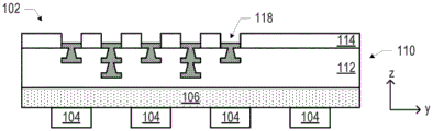
In some embodiments, the antenna board 102 may include an antenna element 104 coupled to an antenna patch support 110 by an adhesive. Fig. 3 shows an antenna board 102 in which an antenna patch support 110 includes a circuit board 112 (e.g., including two to eight PCB layers), solder resist 114 and conductive contacts 118 at one face of the circuit board 112, and adhesive 106 at an opposite face of the circuit board 112. As used herein, "conductive contact" may refer to a portion of a conductive material (e.g., a metal) that serves as an interface between different components; the conductive contacts may be recessed into, flush with, or extend away from the surface of the component, and may take any suitable form (e.g., conductive pads or sockets). The circuit board 112 may include traces, vias, and other structures formed from conductive materials (e.g., metals such as copper) as is known in the art. The conductive structures in the circuit board 112 may be electrically insulated from each other by a dielectric material. Any suitable dielectric material (e.g., laminate) may be used. In some embodiments, the dielectric material may be an organic dielectric material, flame retardant grade 4 material (FR-4), Bismaleimide Triazine (BT) resin, polyimide material, glass reinforced epoxy matrix material, or low-k and ultra-low-k dielectrics (e.g., carbon doped dielectrics, fluorine doped dielectrics, porous dielectrics, and organic polymer dielectrics).
In the embodiment of fig. 3, the antenna element 104 may be adhered to an adhesive 106. The adhesive 106 may be non-conductive, and thus the antenna element 104 may not be electrically coupled to the circuit board 112 through a conductive material path. In some embodiments, the adhesive 106 may be an epoxy. The thickness of the adhesive 106 may control the distance between the antenna element 104 and the adjacent side of the circuit board 112. When the antenna board 102 of fig. 3 (and other figures) is used in the antenna module 100, the IC package 108 may be coupled to some of the conductive contacts 118. In some embodiments, the thickness of the circuit board 112 of fig. 3 may be less than 1 millimeter (e.g., between 0.35 millimeters and 0.5 millimeters). In some embodiments, the thickness of the antenna element 104 may be less than 1 millimeter (e.g., between 0.4 millimeters and 0.7 millimeters).
In some embodiments, the antenna board 102 may include an antenna element 104 coupled to an antenna patch support 110 by soldering. Fig. 4 illustrates an antenna board 102 in which an antenna patch support 110 includes a circuit board 112 (e.g., including two to eight PCB layers), solder resist 114 and conductive contacts 118 at one face of the circuit board 112, and solder resist 114 and conductive contacts 116 at an opposite face of the circuit board 112. The antenna element 104 may be secured to the circuit board 112 by solder 122 (or other second level interconnection) between the conductive contacts 120 and 116 of the antenna element 104. In some embodiments, the conductive contact 116/solder 122/conductive contact 120 may provide a conductive material path through which signals may be transmitted to or from the antenna element 104. In other embodiments, the conductive contact 116/solder 122/conductive contact 120 may be used only for mechanical coupling between the antenna element 104 and the antenna patch support 110. The height of the solder 122 (or other interconnect) may control the distance between the antenna element 104 and the adjacent face of the circuit board 112. Fig. 5 is a top view of an exemplary antenna element 104 that may be used in an antenna plate 102, such as the antenna plate 102 of fig. 4, in accordance with various embodiments. The antenna element 104 of fig. 5 may have a plurality of conductive contacts 120 regularly distributed on one face, near the edges; other antenna elements 104 having conductive contacts 120 may have other arrangements of conductive contacts 120.
In some embodiments, the antenna board may include an antenna element 104 coupled to the bridge structure. Fig. 6 shows an antenna board 102 in which an antenna patch support 110 includes a circuit board 112 (e.g., including two to eight PCB layers), solder resist 114 and conductive contacts 118 at one face of the circuit board 112, and a bridge structure 124 secured to an opposite face of the circuit board 112. The bridge structure 124 may have one or more antenna elements 104 coupled to an inner face of the bridge structure 124 and one or more antenna elements 104 coupled to an outer face of the bridge structure 124. In the embodiment of fig. 6, the antenna element 104 is coupled to the bridge structure 124 by an adhesive 106. In the embodiment of fig. 6, the bridge structure 124 may be coupled to the circuit board 112 by an adhesive 106. The thickness of the adhesive 106 and the dimensions of the bridge structure 124 (i.e., the distance between the inner and adjacent faces of the circuit board 112, and the thickness of the bridge structure 124 between the inner and outer faces) may control the distance between the antenna elements 104 and the adjacent faces of the circuit board 112 (including the distance between the "inner" antenna element 104 and the "outer" antenna element 104). Bridge structure 124 may be formed of any suitable material; for example, the bridge structure 124 may be formed from a non-conductive plastic. In some embodiments, the bridge structure 124 of fig. 6 may be fabricated using three-dimensional printing techniques. In some embodiments, the bridge structure 124 of fig. 6 may be fabricated as a PCB having a recess defining an interior face (e.g., using a recessed plate fabrication technique). In the embodiment of fig. 6, the bridge structure 124 may introduce an air cavity 149 between the antenna element 104 and the circuit board 112, thereby enhancing the bandwidth of the antenna module 100.
Fig. 7 shows an antenna plate 102 similar to the antenna plate 102 of fig. 6, but wherein the bridge structure 124 is curved (e.g., has an arcuate shape). Such bridge structures 124 may be formed of, for example, a flexible plastic or other material. In the antenna board 102 of fig. 7, the antenna patch support 110 includes a circuit board 112 (e.g., including two to eight PCB layers), solder resist 114 and conductive contacts 118 at one face of the circuit board 112, and a bridge structure 124 secured to an opposite face of the circuit board 112. The bridge structure 124 may have one or more antenna elements 104 coupled to an inner face of the bridge structure 124 and one or more antenna elements 104 coupled to an outer face of the bridge structure 124. In the embodiment of fig. 7, the antenna element 104 is coupled to the bridge structure 124 by an adhesive 106. In the embodiment of fig. 6, the bridge structure 124 may be coupled to the circuit board 112 by an adhesive 106. The thickness of the adhesive 106 and the dimensions of the bridge structure 124 (i.e., the distance between the inner and adjacent faces of the circuit board 112, and the thickness of the bridge structure 124 between the inner and outer faces) may control the distance between the antenna elements 104 and the adjacent faces of the circuit board 112 (including the distance between the "inner" antenna element 104 and the "outer" antenna element 104). The bridge structure 124 of fig. 7 may be formed of any suitable material; for example, the bridge structure 124 may be formed from a non-conductive plastic. In the embodiment of fig. 7, the bridge structure 124 may introduce an air cavity 149 between the antenna element 104 and the circuit board 112, thereby enhancing the bandwidth of the antenna module 100.
Fig. 8 shows an antenna plate 102 similar to the antenna plate 102 of fig. 6 and 7, but wherein the bridge structure 124 is itself a planar circuit board or other structure having conductive contacts 126; the bridge structure 124 may be coupled to the circuit board 112 by solder 122 (or other interconnect) between the conductive contacts 126 and the conductive contacts 116 on the circuit board 112. In the antenna board 102 of fig. 8, the antenna patch support 110 includes a circuit board 112 (e.g., including two to eight PCB layers), solder resist 114 and conductive contacts 118 at one face of the circuit board 112, and a bridge structure 124 secured to an opposite face of the circuit board 112. The bridge structure 124 may have one or more antenna elements 104 coupled to an inner face of the bridge structure 124 and one or more antenna elements 104 coupled to an outer face of the bridge structure 124. In the embodiment of fig. 8, the antenna element 104 is coupled to the bridge structure 124 by an adhesive 106. The thickness of the adhesive 106, the height of the solder 122, and the size of the bridge structure 124 (i.e., the thickness of the bridge structure 124 between the inner and outer faces) may control the distance between the antenna element 104 and the adjacent face of the circuit board 112 (including the distance between the "inner" antenna element 104 and the "outer" antenna element 104). The bridge structure 124 of fig. 8 may be formed of any suitable material; for example, bridge structure 124 may be formed from a non-conductive plastic or PCB. In the embodiment of fig. 8, the bridging structure 124 may introduce an air cavity 149 between the antenna unit 104 and the circuit board 112, thereby enhancing the bandwidth of the antenna module 100.
Fig. 9 shows an antenna board 102 similar to the antenna board 102 of fig. 8, but where the bridge structure 124 is itself a planar circuit board or other structure, and both the bridge structure 124 and the antenna elements 104 coupled to the bridge structure are coupled to the circuit board 112 by the adhesive 106. In the antenna board 102 of fig. 9, the antenna patch support 110 includes a circuit board 112 (e.g., including two to eight PCB layers), solder resist 114 and conductive contacts 118 at one face of the circuit board 112, and a bridge structure 124 secured to an opposite face of the circuit board 112. The bridge structure 124 may have one or more antenna elements 104 coupled to an inner face of the bridge structure 124 and one or more antenna elements 104 coupled to an outer face of the bridge structure 124. In the embodiment of fig. 9, the antenna element 104 is coupled to the bridge structure 124 by an adhesive 106. The thickness of the adhesive 106 and the size of the bridge structure 124 (i.e., the thickness of the bridge structure 124 between the inner and outer faces) may control the distance between the antenna element 104 and the adjacent face of the circuit board 112 (including the distance between the "inner" antenna element 104 and the "outer" antenna element 104). The bridge structure 124 of fig. 9 may be formed of any suitable material; for example, bridge structure 124 may be formed from a non-conductive plastic or PCB. In some embodiments, the circuit board 112 may be a 1-2-1 core board and the bridge structure 124 may be a 0-2-0 core board. In some embodiments, the circuit board 112 may use a different dielectric material than that of the bridge structure 124 (e.g., the bridge structure 124 may comprise Polytetrafluoroethylene (PTFE) or a PTFE-based formulation), and the circuit board 112 may comprise another dielectric material).
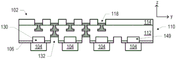
In some embodiments, the antenna board 102 may include a recess "above" the antenna element 104 to provide an air cavity 149 between the antenna element 104 and other portions of the antenna board 102. Fig. 10 shows an antenna plate 102 similar to the antenna plate 102 of fig. 3, but wherein the circuit board 112 includes a recess 130 "above" each antenna element 104. These recesses 130 may provide air cavities 149 between the antenna unit 104 and the rest of the antenna plate 102, which may improve performance. In the embodiment of fig. 10, the antenna patch support 110 includes a circuit board 112 (e.g., including two to eight PCB layers), solder resist 114 and conductive contacts 118 at one face of the circuit board 112, and adhesive 106 at an opposite face of the circuit board 112. The antenna element 104 may be adhered to the adhesive 106. The adhesive 106 may be non-conductive, and thus the antenna element 104 may not be electrically coupled to the circuit board 112 through a conductive material path. In some embodiments, the adhesive 106 may be an epoxy. The thickness of the adhesive 106 may control the distance between the antenna element 104 and the adjacent side of the circuit board 112. In some embodiments, the recess 130 may have a depth of between 200 microns and 400 microns.
In some embodiments, the antenna board 102 may include recesses that are not "above" the antenna elements 104 but are located between the attachment locations of different ones of the antenna elements 104 to the circuit board 112. For example, fig. 11 shows an antenna board 102 similar to the antenna board 102 of fig. 10, but wherein the circuit board 112 includes additional recesses 132 "in between" each of the antenna elements 104. These recesses 132 may help isolate different ones of the antenna elements 104 from one another, thereby improving performance. In the embodiment of fig. 11, the antenna patch support 110 includes a circuit board 112 (e.g., including two to eight PCB layers), solder resist 114 and conductive contacts 118 at one face of the circuit board 112, and adhesive 106 at an opposite face of the circuit board 112. The antenna element 104 may be adhered to the adhesive 106. The adhesive 106 may be non-conductive, and thus the antenna element 104 may not be electrically coupled to the circuit board 112 through a conductive material path. In some embodiments, the adhesive 106 may be an epoxy. The thickness of the adhesive 106 may control the distance between the antenna element 104 and the adjacent side of the circuit board 112. In some embodiments, the recesses 132 may have a depth of between 200 microns and 400 microns. In some embodiments, the recess 132 may be a through-hole (i.e., the recess 132 may extend all the way through the circuit board 112).
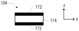
Any suitable antenna structure may provide the antenna elements 104 of the antenna module 100. In some embodiments, the antenna unit 104 may include one, two, three, or more antenna layers. For example, fig. 12 and 13 are side cross-sectional views of an exemplary antenna element 104 according to various embodiments. In fig. 12, the antenna unit 104 includes one antenna patch 172, while in fig. 13, the antenna unit 104 includes two antenna patches 172 spaced apart by an intervening structure 174.
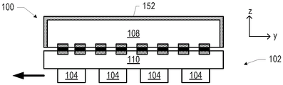
The IC package 108 included in the antenna module 100 may have any suitable structure. For example, fig. 14 shows an exemplary IC package 108 that may be included in the antenna module 100. The IC package 108 may include a package substrate 134 to which one or more components 136 may be coupled through first level interconnects 150. In particular, the conductive contact 146 at one face of the package substrate 134 may be coupled to the conductive contact 148 at the face of the component 136 by a first level interconnect 150. The first level interconnect 150 shown in fig. 14 is a solder bump, but any suitable first level interconnect 150 may be used. The solder resist 114 may be disposed around the conductive contacts 146. The package substrate 134 may include a dielectric material and may have conductive paths (e.g., including conductive vias and lines) extending through the dielectric material between the faces or between different locations on each face. In some embodiments, the package substrate 134 may have a thickness of less than 1 millimeter (e.g., between 0.1 millimeter and 0.5 millimeter). Conductive contacts 144 may be disposed on the other side of the package substrate 134 and second level interconnects 142 may couple these conductive contacts 144 to the antenna board 102 (not shown) in the antenna module 100. The second level interconnects 142 shown in fig. 14 are solder balls (e.g., for a ball grid array arrangement), but any suitable second level interconnects 142 may be used (e.g., pins in a pin grid array arrangement or lands in a land grid array arrangement). The solder resist 114 may be disposed around the conductive contacts 144. In some embodiments, a molding material 140 may be disposed around the component 136 (e.g., between the component 136 and the package substrate 134 as an underfill material). In some embodiments, the thickness of the molding material may be less than 1 millimeter. Exemplary materials that may be used for the molding material 140 include suitable epoxy molding materials. In some embodiments, a conformal shield 152 may be disposed around the component 136 and the package substrate 134 to provide electromagnetic shielding for the IC package 108.
The components 136 may include any suitable IC components. In some embodiments, one or more components 136 may comprise a die. For example, one or more of the components 136 may be an RF communication die. In some embodiments, one or more components 136 may include resistors, capacitors (e.g., decoupling capacitors), inductors, DC-DC converter circuits, or other circuit elements. In some embodiments, the IC package 108 may be a System In Package (SiP). In some embodiments, the IC package 108 may be a Flip Chip (FC) Chip Scale Package (CSP). In some embodiments, one or more of the components 136 may comprise a memory device programmed with instructions to perform beamforming, scanning, and/or codebook functions.
In some embodiments, the antenna patch support 110 of the antenna board 102 may have one or more flexible portions. For example, the antenna patch support 110 may include a flexible PCB (also referred to as a "flex circuit"). The antenna patch support 110 may be flexible in its entirety, or in other embodiments, may have one or more rigid portions and one or more flexible portions; this latter embodiment may be referred to as a "rigid-flexible plate". As used herein, an antenna patch support 110 referred to as having a "flexible portion" may be flexible in its entirety. In some embodiments in which the antenna patch support 110 includes a flexible portion, one or more antenna elements 104 may be disposed on the flexible portion, some antenna elements 104 may be disposed on the flexible portion and some antenna elements 104 may be disposed on the rigid portion (if present), or the antenna elements may not be disposed on the flexible portion. In some embodiments, the flexible portion(s) of the antenna plate 102 may be used to electrically connect the antenna plate 102 to another component (e.g., the circuit board 101 discussed below with reference to fig. 22).
The flexible portion of the antenna patch support 110 may be manufactured using any suitable technique and using any suitable material. For example, the flexible portion of the antenna patch support 110 may include a flexible insulator (e.g., polyimide, polyester, polyethylene terephthalate, polyetheretherketone, etc.) with printed or laminated conductive materials (e.g., copper, aluminum, silver, etc.). The flexible portion of the antenna patch support 110 may have one or more layers of circuitry. In some embodiments, the flexible portion of the antenna patch support 110 may be coupled to one or more local stiffeners to provide mechanical support as needed. In some embodiments, the flexible portion of the antenna patch support 110 may be thinner than other less flexible portions of the antenna patch support 110; for example, when the antenna patch support 110 is a rigid-flexible board, the flexible portion(s) may be thicker than the rigid portion(s).
Any of the antenna boards 102 disclosed herein may include an antenna patch support 110 having a flexible portion. For example, any of the antenna patch support 110 or antenna plate 102 discussed above with reference to fig. 1-11 or discussed below with reference to fig. 18-29 may have one or more flexible portions, or may be part of the antenna patch support 110 having one or more flexible portions. Fig. 15-17 illustrate various examples of an antenna module 100 including a flexible portion; any of the antenna modules 100 of fig. 15-17 may include any of the other structures disclosed herein (e.g., the antenna patch support 110 of the antenna module of fig. 15-17 may include or take the form of any of the antenna patch supports 110 discussed above with reference to fig. 3-11).
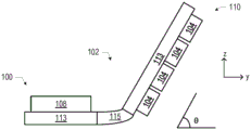
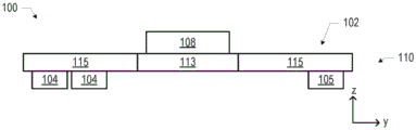
Fig. 15A and 15B show an antenna module 100 comprising an antenna patch support 110 having a flexible portion 115 between two other portions 113; the other portion 113 may be flexible or rigid. The flexible portion 115 may allow the antenna module 100 to bend or twist into a desired configuration without causing significant damage to the antenna patch support 110; fig. 15A shows a "flat configuration", while fig. 15B shows a configuration in which one portion 113 is arranged at an angle θ with respect to the other portion 113. Thus, the flexible portion 115 may act as a hinge to allow the antenna module 100 to bend such that different portions of the antenna module 100 are not coplanar with one another. In the antenna module 100 of fig. 15, the IC package 108 is disposed at one face of the antenna patch support 110 and the plurality of antenna elements 104 are disposed at an opposite face of the antenna patch support 110 (e.g., according to any of the embodiments disclosed herein). In the embodiment of fig. 15, the IC package is coupled to one of the portions 113, and the antenna element 104 is coupled to another one of the portions 113. Antenna module 100, similar to that shown in fig. 15, may be located within a communication device in any desired configuration; for example, an antenna module 100 similar to that shown in fig. 15 may be used in communication device 151 in the manner discussed below with reference to fig. 25 or in the manner discussed below with reference to fig. 26. More generally, antenna module 100 may be mounted in an electronic component (e.g., in communication device 151) in a non-coplanar configuration (e.g., using any of the fixtures discussed herein with reference to fig. 27-32 and 37-38), thereby allowing antenna elements 104 on different sections of antenna board 102 to radiate and receive at different angles, or allowing antenna elements 104 to radiate and receive at angles other than a nominal "planar" arrangement. In some embodiments, the thickness of the flexible portion 115 may be less than the thickness of the other portion 113. In some embodiments, the other portion 113 may be rigid (and thus the antenna patch support 110 may be a rigid-flexible board). In some embodiments, the antenna module 100 of fig. 15 may include additional flexible portions 115 or other portions 113 (not shown). In some embodiments, the IC package 108 and the antenna element 104 may be disposed on the same side of the antenna patch support 110 of fig. 15.
In some embodiments, flexible portion 115 may be used to carry control and/or RF signals to various other electronic components in communication device 151, thereby eliminating or mitigating the need for additional connectors and cables. For example, such control lines may control how the antenna elements 114 and the IC package 108 (e.g., active RF IC chip) interact. RF signals carried by the flexible portion 115 may carry transmit signals from a circuit board (e.g., the circuit board 101 discussed below, which may be a motherboard), and these RF signals may be radiated by the antenna element (e.g., after post-processing by the antenna module 100).
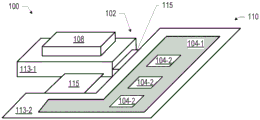
In some embodiments, the antenna module 100 may include a plurality of flexible portions 115 between a pair of other portions 113. For example, fig. 15C is a perspective view of the antenna module 100, where a portion 113-1 (e.g., a rigid portion) is coupled to another portion 113-2 (e.g., a rigid portion) by two flexible portions 115. Portion 113-2 may have an "L-shape" and may extend around portion 113-1 as shown, with each of flexible portions 115 coupled to a different "leg" of portion 113-2. In some embodiments of the antenna module 100 of fig. 15C, the large antenna element 104-1 may be disposed (e.g., printed) on the portion 113-2 and one or more smaller antenna elements 104-2 may be disposed (e.g., printed) within the boundaries of the large antenna element 104-1. Large antenna element 104-1 may communicate at a lower frequency than smaller antenna element 104-2 and, therefore, operation of large antenna element 104-1 may not interfere with operation of smaller antenna element 104-2 (and vice versa). For example, antenna unit 104-1 may be a WiFi, Long Term Evolution (LTE), or Global Navigation Satellite System (GNSS) antenna, while antenna unit 104-2 may be a millimeter wave antenna. In some embodiments, the large antenna element 104-1 may be a planar inverted-F antenna (PIFA).
Fig. 16A shows an antenna module 100 comprising an antenna patch support 110 having two flexible portions 115 with another portion 113 between the flexible portions 115; the further portion 113 may be flexible or rigid. Although the flexible portions 115 of the antenna module 100 of fig. 16 are shown as being substantially coplanar with one another, this is merely one configuration; as discussed above with reference to fig. 15, the flexible portion 115 may be bent or twisted into a desired configuration. In the antenna module 100 of fig. 16, the IC package 108 is disposed at one face of the antenna patch support 110 and the plurality of antenna elements 104 are disposed at an opposite face of the antenna patch support 110 (e.g., according to any of the embodiments disclosed herein). In the embodiment of fig. 16, an IC package is coupled to portion 113, and one or more antenna elements 104 are coupled to each of flexible portions 115. Antenna module 100, similar to that shown in fig. 16, may be positioned within a communication device in any desired configuration; for example, an antenna module 100 similar to that shown in fig. 15 may be used in communication device 151 in the manner discussed below with reference to fig. 25 or in the manner discussed below with reference to fig. 26. More generally, antenna module 100 may also be mounted in an electronic component (e.g., in communication device 151) in a non-coplanar configuration (e.g., using any of the fixtures discussed herein with reference to fig. 27-32 and 37-38), thereby allowing antenna elements 104 on different sections of antenna board 102 to radiate and receive at different angles, or allowing antenna elements 104 to radiate and receive at angles other than a nominal "planar" arrangement. In some embodiments, the thickness of the flexible portion 115 may be less than the thickness of the other portion 113. In some embodiments, the other portion 113 may be rigid (and thus the antenna patch support 110 may be a rigid-flexible board). In some embodiments, the antenna module 100 of fig. 16 may include additional flexible portions 115 or other portions 113 (not shown). In some embodiments, the IC package 108 and the antenna element 104 may be disposed on the same side of the antenna patch support 110 of fig. 16.
As discussed above with reference to fig. 15, the flexible portion 115 of the antenna patch support 110 may allow the antenna module 100 to be arranged in any of a plurality of orientations. For example, fig. 16B shows antenna module 100 having a flexible portion 115 that "folds" over portion 113 causing associated antenna element 104 to radiate in a direction above IC package 108 (and may use, for example, the ground of IC package 108 as a reference); the antenna element 104 located on the further flexible portion 115 (and/or on the bottom surface of the portion 113, not shown) may radiate in a direction below the IC package 108. Thus, an antenna module 100 similar to that shown in fig. 16B may achieve radiation in all or many directions. An arrangement in which one or more antenna elements 104 are located "above" the IC package 108 may also allow the antenna module 100 disclosed herein to utilize space available "above" the IC package 108 in the communication device 151, but is not limited to space available "below" the IC package 108.
Fig. 17 shows an antenna module 100 similar to the antenna module 100 of fig. 16, but with the antenna element 104 disposed on one of the flexible portions 115 and the connector 105 disposed on the other of the flexible portions 115. The connector 105 may be used to transmit signals into and out of the antenna module 100. In some embodiments, the connector 105 may be a coaxial cable connector or any other connector (e.g., a flat cable connector discussed below with reference to fig. 37 and 38). The connector 105 may be adapted to transmit RF signals, for example, and may be used instead of or in addition to cables in the antenna module 100 of fig. 17. Although a single connector 105 is shown in fig. 17, the antenna module 100 may include one or more connectors 105. Further, although the connector 105 is shown in fig. 17 as being located on the same face of the antenna patch support 110 as the antenna element 104, the connector 105 may be located on an opposite face of the antenna patch support 110. More generally, the elements of the antenna module 100 of fig. 17 may take the form of any of the embodiments discussed above with reference to fig. 16.
The array of antenna elements 104 in the antenna module 100 may be used in any of a variety of ways. For example, the array of antenna elements 104 may be used as a broadside array or an end-fire array. In some embodiments, where the array of antenna elements 104 is used as an end-fire array, the sides of the conformal shield 152 on the IC package 108 may provide a reflector or ground plane for the end-fire array. For example, fig. 18 shows an exemplary antenna module 100 in which an array of antenna elements 104 is used as an end-fire array, with the transmission pointing in the direction indicated by the bold array; in this embodiment, the portion of the conformal shield 152 on the side of the IC package 108 may serve as a reflector or ground plane for operation of the array of antenna elements 104 as an end-fire array. Although a particular antenna module 100 is shown in fig. 18, any suitable antenna module of the antenna modules 100 disclosed herein may operate as an end-fire array as described with reference to fig. 18.
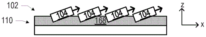
In an antenna module 100 including multiple antenna elements 104, the multiple antenna elements 104 may be arranged in any suitable manner. For example, fig. 19 and 20 are bottom views of exemplary arrangements of antenna elements 104 in antenna plate 102 according to various embodiments. In the embodiment of fig. 19, the antenna elements 104 are arranged in a linear array in the x-direction, and the x-axis of each antenna element 104 (indicated in fig. 19 by a small arrow near each antenna element 104) is aligned with the axis of the linear array. In other embodiments, the antenna elements 104 may be arranged such that one or more of their axes are not aligned with the direction of the array. For example, fig. 20 shows an embodiment in which the antenna elements 104 are distributed in a linear array in the x-direction, but the antenna elements 104 have been rotated in the x-y plane (relative to the embodiment of fig. 19) such that the x-axis of each antenna element 104 is not aligned with the axis of the linear array. In another example, fig. 21 shows an embodiment in which the antenna elements 104 are distributed in a linear array in the x-direction, but the antenna patch has been rotated in the x-z plane (relative to the embodiment of fig. 19) such that the x-axis of each antenna element 104 is not aligned with the axis of the linear array. In the embodiment of fig. 21, antenna patch support 110 may include an antenna board mount 164 that may hold antenna unit 104 at a desired angle. In some embodiments, the "rotations" of fig. 20 and 21 may be combined such that when antenna element 104 is part of a linear array distributed in the x-direction, antenna element 104 rotates in both the x-y and x-z planes. In some embodiments, some, but not all, of the antenna elements 104 in a linear array may be "rotated" relative to the axis of the array. Rotating the antenna elements 104 relative to the direction of the array may reduce patch-to-patch coupling (by reducing the constructive addition of resonant currents between the antenna elements 104), thereby improving impedance bandwidth and beam steering range. The arrangements of fig. 19-21 (and combinations of such arrangements) are referred to herein as "rotational offsets" of the antenna elements 104 from the linear array.
Although fig. 19-21 show multiple antenna elements 104 mounted on a common antenna patch support 110 in a single antenna plate 102, the rotational offset arrangement of fig. 19-21 may also be utilized when multiple antenna elements 104 are divided between different antenna plates 102. For example, in an embodiment in which multiple different antenna boards 102 are mounted to a common IC package 108, the antenna elements 104 in each different antenna board 102 may together provide a linear array and may be rotationally offset from the linear array.
The antenna module 100 disclosed herein may be included in any suitable communication device (e.g., a computing device with wireless communication capabilities, a wearable device with wireless communication circuitry, etc.). Fig. 22 is a side cross-sectional view of a portion of a communication device 151 including an antenna module 100, in accordance with various embodiments. In particular, the communication device 151 shown in fig. 22 may be a handheld communication device, such as a smartphone or a tablet computer. The communication device 151 may include a glass or plastic back cover 176 proximate to a metal or plastic housing 178. In some embodiments, the chassis 178 may be laminated to the interior face of the back cover 176 or attached to the back cover 176 with an adhesive. In some embodiments, the portion of the casing 178 adjacent to the back cover 176 may have a thickness between 0.1 millimeters and 0.4 millimeters; in some such embodiments, the portion of the housing 178 may be formed of metal. In some embodiments, the back cover 176 may have a thickness between 0.3 millimeters and 1.5 millimeters; in some such embodiments, the back cover 176 may be formed of glass. Housing 178 may include one or more windows 181 aligned with antenna elements 104 (not shown) of antenna module 100 to improve performance. An air cavity 180-1 may separate at least some of the antenna module 100 from the back cover 176. In some embodiments, the height of the air cavity 180-1 may be between 0.5 millimeters and 3 millimeters. In some embodiments, the antenna module 100 may be mounted to one face of a circuit board 101 (e.g., a motherboard) and other components 129 (e.g., other IC packages) may be mounted to an opposite face of the circuit board 101. In some embodiments, the circuit board 101 may have a thickness between 0.2 millimeters and 1 millimeter (e.g., between 0.3 millimeters and 0.5 millimeters). Another air cavity 180-2 may be located between the circuit board 101 and a display 182 (e.g., a touch screen display). In other embodiments, the antenna module 100 may not be mounted to the circuit board 101; instead, the antenna module 100 may be secured directly to the housing 178 (e.g., as described below). In some embodiments, the spacing between the antenna element 104 (not shown) and the back cover 176 of the antenna module 100 may be selected and controlled to within tens of microns to achieve desired performance. The air cavity 180-2 may separate the antenna module 100 from the display 182 on the front side of the communication device 151; in some embodiments, display 182 may have a metal layer near air cavity 180-2 to draw heat away from display 182. A metal or plastic housing 184 may provide the "side" of the communication device 151.
The antenna module 100 may be coupled to the circuit board 101 in the communication device 151 in any suitable manner. For example, the antenna module 100 may include a connector 105 to which a cable (e.g., a coaxial cable or a flat printed circuit cable) may be mated; the other end of the cable may mate with a connector 105 (not shown) on the circuit board 101. In some embodiments, the antenna module 100 and the connector 105 on the circuit board 101 may mate directly with each other without the use of an intermediate cable. For example, fig. 23 and 24 illustrate two different arrangements in which connector 105-1 of antenna module 100 directly mates with connector 105-2 on circuit board 101 to electrically couple antenna module 100 and circuit board 101. The connector 105-1 of the antenna module 100 may be mounted on the antenna board 102 or on the IC package 108 as desired. In the embodiment of fig. 23, circuit board 101 and antenna module 100 are oriented such that circuit board 101 is substantially "above" antenna module 100; in the embodiment of fig. 24, circuit board 101 and antenna module 100 are oriented such that circuit board 101 and antenna module 100 are "offset" from each other. The connector 105 may take any suitable form; for example, the connector 105 may be a coaxial connector adapted to transmit RF signals between the antenna module 100 and the circuit board 101. In addition, although a single connector 105 is shown for each of the antenna module 100 and the circuit board 101, the antenna module 100 and the circuit board 101 may be coupled together by a plurality of connectors 105. Such an embodiment may eliminate the need for cables between antenna module 100 and circuit board 101, thereby reducing the complexity and bulk of the components in communication device 151.
As described above, antenna module 100, including flexible portion 115, may be oriented in communication device 151 in any suitable manner. In particular, the antenna module 100 with the flexible portion 115 may be used to orient an array of antenna elements 104 in a communication device such that the antenna elements 104 are disposed at a desired angle relative to the display 182, the rear cover 176, and/or the housing 184. In some embodiments, an antenna module 100 in which an array of antenna elements 104 is "tilted" relative to a display 182, back cover 176, and/or housing 184 may achieve a combination of broadside radiation coverage and broadside radiation coverage from the same array. In some embodiments, the angle at which the antenna elements 104 are disposed in the communication device 151 may be selected to tune the array radiation direction to achieve a desired spatial coverage depending on the integration environment (e.g., handheld communication device 151 with glass back cover 176) and the desired application.
For example, fig. 25 shows a communication device 151 that includes a first antenna module 100-1 that is substantially "flat" and a second antenna module 100-2 having a flexible portion 115 that acts as a hinge, allowing different portions of the antenna module 100-2 to be non-coplanar with one another. Fig. 25A is an "exploded" view showing antenna module 100 external to communication device 151, while fig. 25B shows antenna module 100 located in communication device 151.
In the embodiment of fig. 25, the antenna module 100-1 includes an IC package 108 on one face of the antenna board 102, with an array of antenna elements 104 on the opposite face. The antenna module 100-1 may be located in the communication device 151 such that the array of antenna elements 104 is arranged parallel to and proximate to the window 181 in the back cover 176; the window 181 may allow for improved transmission of RF signals between the antenna module 100-1 and the external environment relative to embodiments in which the window 181 is not present. In some embodiments, antenna module 100-1 may generate radiation beams for both 5G communication channels and 60 gigahertz communication channels. In some embodiments, an audio speaker (not shown) may be proximate to antenna module 100-1 and may emit an audio signal through window 181. The window 181 may have any suitable size; for example, in some embodiments, the window 181 may have an area between 50 square millimeters and 200 square millimeters (e.g., between 75 square millimeters and 125 square millimeters). In some embodiments, window 181 may not be present. Window 179 may also be present in housing 178 proximate to rear cover 176 (not shown in fig. 25). In some embodiments, window 179 may not be present.
The antenna module 100-2 of fig. 25 includes an IC package 108 on the same face of the antenna board 102 as the array of antenna elements 104; the antenna module 100-2 may have a substantially similar form as discussed above with reference to fig. 15, but with the IC package 108 and the antenna element 104 on the same side of the antenna patch support 110. The flexible portion 115 of the antenna module 100-2 may act as a hinge, allowing the antenna module 100-2 to be positioned in the communication device 151 such that the portion of the antenna patch support 110 (not labeled in fig. 25) coupled with the IC package 108 may be parallel to the back cover 176 and the portion of the antenna patch support 110 coupled with the antenna element 104 may be perpendicular to the back cover 176 (and parallel to the side of the communication device 151 provided by the housing 184). In some embodiments, antenna module 100-2 may generate radiation beams for both 5G communication channels and 60 gigahertz communication channels. In some embodiments, a window 187 may be present in housing 184; the array of antenna elements 104 may be arranged parallel to and proximate to the window 187. Relative to embodiments in which window 187 is not present, window 187 may allow for improved transmission of RF signals between antenna module 100-2 and the external environment. Window 187 may have any suitable size; for example, in some embodiments, the window 187 can have an area between 50 square millimeters and 200 square millimeters (e.g., between 75 square millimeters and 125 square millimeters, or a rectangle having dimensions approximately equal to 5 millimeters by 18 millimeters). In some embodiments, window 187 may not be present.
Fig. 26 shows another exemplary communication device 151 including a first antenna module 100-1 and a second antenna module 100-2. The first and second antenna modules 100 of fig. 26 each have a flexible portion 115 that acts as a hinge, allowing different portions of the antenna modules 100 to be non-coplanar with one another. Fig. 26A is an "exploded" view showing antenna module 100 external to communication device 151, while fig. 26B shows antenna module 100 located in communication device 151.
In the embodiment of fig. 26, the antenna module 100 includes an IC package 108 on the same face of the antenna board 102 as the array of antenna elements 104; the antenna module 100 may have a substantially similar form as discussed above with reference to fig. 15, but with the IC package 108 and the antenna element 104 on the same side of the antenna patch support 110. The flexible portion 115 of the antenna module 100 may act as a hinge, allowing the antenna module 100 to be positioned in the communication device 151 such that the portion of the antenna patch support 110 (not labeled in fig. 26) to which the IC package 108 is coupled may be parallel to the back cover 176 and the portion of the antenna patch support 110 to which the antenna unit 104 is coupled may be positioned at an angle that is neither parallel nor perpendicular to the back cover 176 (and neither parallel nor perpendicular to the sides of the communication device 151 provided by the housing 184). For example, the antenna unit 104 may be oriented at a 45 degree angle with respect to the back cover 176/housing 184. In some embodiments, windows 187-1 and 187-2 may be present in housing 184; the arrays of antenna elements 104 of antenna modules 100-1 and 100-2 may be disposed adjacent windows 187-1 and 187-2, respectively. These windows 187 may allow for improved transmission of RF signals between antenna modules 100 as described above. In some embodiments, there may be one or fewer windows 187.
The antenna module 100 disclosed herein may be secured in a communication device in any desired manner. For example, as described above, in some embodiments, antenna module 100 may be secured to housing 178. The various embodiments discussed below relate to fasteners that secure the antenna module 100 (or antenna board 102, for ease of illustration) to the chassis 178 of the communication device, but any of the fasteners discussed below may be used to secure the antenna module 100 to any suitable portion of the communication device. For example, in some embodiments, the portion of the antenna plate 102 that may be secured may be the flexible portion 115 or other portion 113 of the antenna patch support 110, as discussed above.
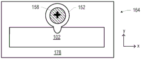
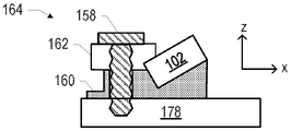
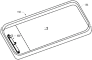
In some embodiments, the antenna plate 102 may include a cutout, which may be used to secure the antenna plate 102 to the chassis 178. For example, fig. 27 is a top view of an exemplary antenna plate 102 that includes two cutouts 154 at either longitudinal end of the antenna plate 102. The antenna board 102 of fig. 27 may be part of the antenna module 100, but for convenience of explanation, only the antenna board 102 is depicted in fig. 27. Fig. 28 is a side cross-sectional view of the antenna plate 102 of fig. 27 coupled to an antenna plate mount 164, in accordance with various embodiments. In particular, the antenna plate mount 164 of fig. 28 may include two components at either longitudinal end of the antenna plate 102. Each assembly may include a boss 160 (on or as part of the housing 178), a spacer 162 on the top surface of the boss 160, and a screw 158 extending through a hole in the spacer 162 and threaded into a thread in the boss 160. The antenna plate 102 may be clamped between the spacer 162 and the top of the boss 160 by a tightened screw 158; the boss 160 may be at least partially disposed in the proximal cutout 154. In some embodiments, the outer dimensions of the antenna plate 102 of fig. 27 may be about 5 millimeters by about 38 millimeters.
In some embodiments, the screws 158 disclosed herein may be used to dissipate heat generated by the antenna module 100 during operation. In particular, in some embodiments, the screws 158 may be formed of metal, and the bosses 160 and the casing 178 may also be metallic (or may otherwise have high thermal conductivity); during operation, heat generated by the antenna module 100 may be transferred away from the antenna module 100 through the screws 158 and into the housing 178, thereby mitigating or preventing an overheating condition. In some embodiments, a Thermal Interface Material (TIM), such as thermal grease, may be present between antenna plate 102 and screws 158/bosses 160 to improve thermal conductivity.
In some embodiments, the screws 158 disclosed herein may be used as additional antennas for the antenna module 100. In some such embodiments, the boss 160 (and other materials with which the screw 158 contacts) may be formed of plastic, ceramic, or other non-conductive material. The shape and position of the screw 158 are selected such that the screw 158 functions as the antenna unit 104 for the antenna board 102.
The antenna board 102 may include other arrangements of cutouts. For example, fig. 29 is a top view of an exemplary antenna plate 102 that includes a cutout 154 at one longitudinal end and a hole 168 near the other longitudinal end. The antenna board 102 of fig. 29 may be part of the antenna module 100, but for convenience of explanation, only the antenna board 102 is depicted in fig. 29. Fig. 30 is a side cross-sectional view of the antenna plate 102 of fig. 29 coupled to an antenna plate mount 164, in accordance with various embodiments. In particular, the antenna plate mount 164 of fig. 30 may include two components at either longitudinal end of the antenna plate 102. The assembly adjacent to the cutout 154 may include the boss 160/spacer 162/screw 158 arrangement discussed above with reference to fig. 28. The components proximate to the aperture 168 may include a pin 170 extending from a housing 178. The antenna plate 102 may be clamped between the spacer 162 and the top of the boss 160 by a set screw 158 at one longitudinal end (the boss 160 may be at least partially disposed adjacent the cutout 154) and the other longitudinal end may be prevented from moving in the x-y plane by a pin 170 in the hole 168.
In some embodiments, the antenna module 100 may be secured to the communication device at one or more locations along the length of the antenna plate 102 in addition to or instead of at the longitudinal ends of the antenna plate 102. For example, fig. 31A and 31B are top and side cross-sectional views, respectively, of an antenna plate 102 coupled to an antenna plate mount 164, according to various embodiments. The antenna board 102 of fig. 31 may be part of the antenna module 100, but for convenience of explanation, only the antenna board 102 is depicted in fig. 31. In the antenna board mount 164 of fig. 31, a boss 160 (one or part of the chassis 178), a spacer 162 on the top surface of the boss 160, and a screw 158 extending through a hole in the spacer 162 and screwed into the thread of the boss 160. The exterior of the boss 160 of fig. 31 may have a square cross-section, and the spacer 162 may have a square recess on its lower surface to partially wrap around the boss 160 while preventing rotation around the boss 160. The antenna plate 102 may be clamped between the spacer 162 and the top of the boss 160 by a tightened screw 158. In some embodiments, the antenna plate 102 may not have a cutout 154 along its longitudinal length (as shown); while in other embodiments, the antenna plate 102 may also have one or more cutouts 154 along its long sides.
In some embodiments, antenna module 100 may be secured to a surface in a communication device such that antenna module 100 (e.g., an array of antenna elements 104 in the antenna module) is not parallel to the surface. In general, the antenna unit 104 may be positioned at any desired angle relative to the housing 178 or other element of the communication device. Fig. 32 shows an antenna board mount 164 in which the antenna board 102 may be held at an angle relative to the lower surface of the casing 178. The antenna board 102 of fig. 32 may be part of the antenna module 100, but for convenience of explanation, only the antenna board 102 is depicted in fig. 32. Antenna plate mount 164 may be similar to the antenna plate mount of fig. 28, 30, and 31, but may include a boss 160 having an angled portion on which antenna plate 102 may rest. When the screws 158 are tightened, the antenna plate 102 may be held at a desired angle relative to the casing 178.
The antenna board 102, IC package 108, and other elements disclosed herein may be arranged in the antenna module 100 in any suitable manner. For example, the antenna module 100 may include one or more connectors 105 for transmitting signals into and out of the antenna module 100. Fig. 33-36 are exploded perspective views of an exemplary antenna module 100 according to various embodiments.
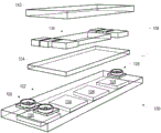
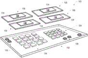
In the embodiment of fig. 33, the antenna board 102 includes four antenna elements 104. The antenna elements 104 may be disposed in the antenna board 102 (e.g., with the recess 130/132, rotated relative to an axis of the array, on the bridge structure 124, etc.) according to any of the embodiments disclosed herein. One or more connectors 105 may be provided on the antenna board 102; these connectors 105 may be coaxial cable connectors as shown, or any other connector (e.g., flat cable connectors discussed below with reference to fig. 37 and 38). The connector 105 may be adapted to transmit RF signals, for example. The IC package 108 may include a package substrate 134, one or more components 136 coupled to the package substrate 134, and a conformal shield 152 over the components 136 and the package substrate 134. In some embodiments, four antenna elements 104 may provide a 1 × 4 array for 28/39 gigahertz communications, and a 1 × 8 array of 60 gigahertz dipoles.
In the embodiment of fig. 34, the antenna panel 102 comprises two sets of sixteen antenna elements 104, each set being arranged in a 4 x 4 array. The antenna elements 104 may be disposed in the antenna board 102 (e.g., with the recess 130/132, rotated relative to an axis of the array, on the bridge structure 124, etc.) according to any of the embodiments disclosed herein. The antenna module 100 of fig. 34 includes two IC packages 108; one IC package 108 is associated with (and disposed over) one set of antenna elements 104 and another IC package 108 is associated with (and disposed over) another set of antenna elements 104. In some embodiments, one set of antenna elements 104 may support 28 gigahertz communications and another set of antenna elements 104 may support 39 gigahertz communications. The IC package 108 may include a package substrate 134, one or more components 136 coupled to the package substrate 134, and a conformal shield 152 over the components 136 and the package substrate 134. One or more connectors 105 may be disposed on the package substrate 134; these connectors 105 may be coaxial cable connectors as shown, or any other connector (e.g., flat cable connectors discussed below with reference to fig. 37 and 38). The conformal shield 152 may not extend over the connector 105. In some embodiments, the antenna module 100 of fig. 34 may be suitable for use in routers and Customer Premises Equipment (CPE). In some embodiments, the outer dimensions of the antenna plate 102 may be about 22 millimeters by about 40 millimeters.
In the embodiment of fig. 35, the antenna board 102 comprises two sets of four antenna elements 104, each set being arranged in a 1 × 4 array. In some embodiments, one set of antenna elements 104 may support 28 gigahertz communications and another set of antenna elements 104 may support 39 gigahertz communications. The antenna elements 104 may be disposed in the antenna board 102 (e.g., with the recess 130/132, rotated relative to an axis of the array, on the bridge structure 124, etc.) according to any of the embodiments disclosed herein. One or more connectors 105 may be provided on the antenna board 102; these connectors 105 may be coaxial cable connectors as shown, or any other connector (e.g., flat cable connectors discussed below with reference to fig. 37 and 38). The antenna module 100 of fig. 35 includes two IC packages 108; one IC package 108 is associated with (and disposed over) one set of antenna elements 104 and another IC package 108 is associated with (and disposed over) another set of antenna elements 104. The IC package 108 may include a package substrate 134, one or more components 136 coupled to the package substrate 134, and a conformal shield 152 over the components 136 and the package substrate 134. In some embodiments, the outer dimensions of the antenna plate 102 may be about 5 millimeters by about 32 millimeters.
In the embodiment of fig. 36, the antenna panel 102 includes two sets of sixteen antenna elements 104, each set arranged in a 4 x 4 array. The antenna elements 104 may be disposed in the antenna board 102 (e.g., with the recess 130/132, rotated relative to an axis of the array, on the bridge structure 124, etc.) according to any of the embodiments disclosed herein. The antenna module 100 of fig. 36 includes four IC packages 108; two IC packages 108 associated with (and disposed over) one set of antenna elements 104, and two other IC packages 108 associated with (and disposed over) another set of antenna elements 104. The IC package 108 may include a package substrate 134, one or more components 136 coupled to the package substrate 134, and a conformal shield (not shown) over the components 136 and the package substrate 134. One or more connectors 105 may be provided on the antenna board 102; these connectors 105 may be coaxial cable connectors as shown, or any other connector (e.g., flat cable connectors discussed below with reference to fig. 37 and 38).
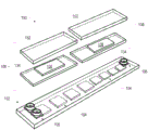
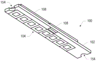
Fig. 37A and 37B are top and bottom perspective views, respectively, of another exemplary antenna module 100 according to various embodiments. In the embodiment of fig. 37, the antenna board 102 comprises two sets of four antenna elements 104, each set being arranged in a 1 × 4 array. The antenna elements 104 may be disposed in the antenna board 102 (e.g., with the recess 130/132, rotated relative to an axis of the array, on the bridge structure 124, etc.) according to any of the embodiments disclosed herein. One or more connectors 105 may be provided on the antenna board 102; these connectors 105 may be flat cable connectors (e.g., Flexible Printed Circuit (FPC) cable connectors) to which the flat cables 196 may be coupled. The antenna module 100 of fig. 35 includes two IC packages 108; one IC package 108 is associated with (and disposed over) one set of antenna elements 104 and another IC package 108 is associated with (and disposed over) another set of antenna elements 104. The antenna module 100 of fig. 35 may also include a cutout 154 at either longitudinal end; fig. 37A shows the antenna module 100 secured by the antenna board mount 164 of fig. 28 (at either longitudinal end) and by the antenna board mount 164 of fig. 31 (in the middle). In some embodiments, the antenna elements 104 of the antenna module 100 of fig. 37 may use the adjacent edges of the antenna plate 102 for both vertically and horizontally polarized edge-fire antennas; in such embodiments, the conformal shield 152 of the IC package 108 may be used as a reference. More generally, the antenna elements 104 disclosed herein may be suitably used for broadside or edge-fire applications.
Any suitable communication device may include one or more of the antenna modules 100 disclosed herein. For example, fig. 38 is a perspective view of a handheld communication device 198 including an antenna module 100, in accordance with various embodiments. In particular, fig. 38 depicts the antenna module 100 of fig. 37 (and associated antenna board mount 164) coupled to the housing 178 of a handheld communication device 198 (which may be the communication device 151 of fig. 22). In some embodiments, the handheld communication device 198 may be a smartphone.
Fig. 39 is a perspective view of a laptop communication device 190 including multiple antenna modules 100, in accordance with various embodiments. In particular, fig. 38 depicts an antenna module 100 having four antenna elements 104 on either side of the keyboard of a laptop communication device 190. The antenna unit 104 may occupy an area on the outer housing of the laptop communication device 190 that is approximately equal to or less than the area required by two adjacent Universal Serial Bus (USB) connectors (i.e., approximately 5 millimeters (height) by 22 millimeters (width) by 2.2 millimeters (depth)). The antenna module 100 of fig. 39 may be tuned to operate in the housing (e.g., ABS plastic) of the device 190. In some embodiments, the antenna module 100 in the device 190 may be tilted at a desired angle relative to the housing of the device 190.
The antenna module 100 included in a communication device (e.g., a fixed wireless access device) may include an antenna array having any desired number of antenna elements 104 (e.g., 4 x 8 antenna elements 104).
Although the various figures of the drawings have illustrated the antenna board 102 as having a larger footprint than the IC package 108, the antenna board 102 and the IC package 108 (which may be, for example, a SiP) may have any suitable relative dimensions. For example, in some embodiments, the footprint of the IC package 108 in the antenna module 100 may be larger than the footprint of the antenna board 102. Such an embodiment may occur, for example, when the IC package 108 includes multiple dies as the components 136.
The antenna module 100 disclosed herein may include or be included in any suitable electronic components. Fig. 40-43 illustrate various examples of devices that may be included or included in any of the antenna modules 100 disclosed herein.
Fig. 40 is a top view of a wafer 1500 and a die 1502 that may be included in any of the antenna modules 100 disclosed herein. For example, the die 1502 may be included in the IC package 108 (e.g., as part 136) or in the antenna unit 104. Wafer 1500 may be comprised of semiconductor material and may include one or more dies 1502 having IC structures formed on a surface of wafer 1500. Each die 1502 may be a repeating unit of a semiconductor product including any suitable IC. After fabrication of the semiconductor product is complete, the wafer 1500 may undergo a dicing process in which the dies 1502 are separated from each other to provide discrete "chips" of the semiconductor product. Die 1502 may include one or more transistors (e.g., some of transistors 1640 of fig. 41 discussed below) and/or supporting circuitry to route electrical signals to the transistors, as well as any other IC components. In some embodiments, wafer 1500 OR die 1502 may include memory devices (e.g., Random Access Memory (RAM) devices such as static RAM (sram) devices, magnetic RAM (mram) devices, resistive RAM (rram) devices, conductive bridging RAM (cbram) devices, etc.), logic devices (e.g., AND, OR, NAND, OR NOR gates), OR any other suitable circuit elements. Multiple of these devices may be combined on a single die 1502. For example, a memory array formed from a plurality of memory devices may be formed on the same die 1502 as a processing device (e.g., processing device 1802 of fig. 43) or other logic configured to store information in the memory devices or execute instructions stored in the memory array.
Fig. 41 is a side cross-sectional view of an IC device 1600 that may be included in any of the antenna modules 100 disclosed herein. For example, IC device 1600 may be included in IC package 108 (e.g., as component 136). IC device 1600 may be formed on a substrate 1602 (e.g., wafer 1500 of fig. 40) and may be included in a die (e.g., die 1502 of fig. 40). Substrate 1602 may be a semiconductor substrate comprised of a semiconductor material system including, for example, an n-type or p-type material system (or a combination of both). Substrate 1602 may comprise a crystalline substrate formed using, for example, bulk silicon or a silicon-on-insulator (SOI) substructure. In some embodiments, substrate 1602 may be formed using alternative materials that may or may not be combined with silicon, including but not limited to germanium, indium antimonide, lead telluride, indium arsenide, indium phosphide, gallium arsenide, or gallium antimonide. Additional materials classified as groups II-VI, III-V, or IV may also be used to form substrate 1602. Although a few examples of materials from which substrate 1602 may be formed are described here, any material that may serve as a basis for IC device 1600 may be used. Substrate 1602 may be a portion of a singulated die (e.g., die 1502 of fig. 40) or a wafer (e.g., wafer 1500 of fig. 40).
The IC device 1600 can include one or more device layers 1604 disposed on a substrate 1602. The device layer 1604 may include features of one or more transistors 1640, such as Metal Oxide Semiconductor Field Effect Transistors (MOSFETs), formed on the substrate 1602. The device layer 1604 may include, for example, one or more source and/or drain (S/D) regions 1620, a gate 1622 for controlling current flow in a transistor 1640 between the S/D regions 1620, and one or more S/D contacts 1624 for routing electrical signals to/from the S/D regions 1620. The transistor 1640 may include additional features not depicted for clarity, such as device isolation regions, gate contacts, etc. The transistors 1640 are not limited to the types and configurations depicted in fig. 41, and may comprise a wide variety of other types and configurations, such as, for example, planar transistors, non-planar transistors, or a combination of both. The planar transistor may include a Bipolar Junction Transistor (BJT), a Heterojunction Bipolar Transistor (HBT), or a High Electron Mobility Transistor (HEMT). Non-planar transistors may include FinFET transistors, such as double-gate or triple-gate transistors, as well as wrap-around or fully-wrap-around gate transistors, such as nanoribbon and nanowire transistors.
Each transistor 1640 may include a gate 1622, a gate dielectric, and a gate electrode formed of at least two layers. The gate dielectric may comprise a layer or a stack of layers. The one or more layers may include silicon oxide, silicon dioxide, silicon carbide, and/or high-k dielectric materials. The high-k dielectric material may include elements such as hafnium, silicon, oxygen, titanium, tantalum, lanthanum, aluminum, zirconium, barium, strontium, yttrium, lead, scandium, niobium, and zinc. Examples of high-k materials that may be used in the gate dielectric include, but are not limited to, hafnium oxide, hafnium silicon oxide, lanthanum aluminum oxide, zirconium silicon oxide, tantalum oxide, titanium oxide, barium strontium titanium oxide, barium titanium oxide, strontium titanium oxide, yttrium oxide, aluminum oxide, lead scandium tantalum oxide, and lead zinc niobate. In some embodiments, when a high-k material is used, an annealing process may be performed on the gate dielectric to improve its quality.
The gate electrode may be formed on a gate dielectric and may include at least one p-type workfunction metal or n-type workfunction metal, depending on whether transistor 1640 is a p-type metal oxide semiconductor (PMOS) transistor or an n-type metal oxide semiconductor (NMOS) transistor. In some implementations, the gate electrode can be comprised of a stack of two or more metal layers, where one or more metal layers are work function metal layers and at least one metal layer is a fill metal layer. Additional metal layers, such as barrier layers, may be included for other purposes. For a PMOS transistor, metals that may be used for the gate electrode include, but are not limited to, ruthenium, palladium, platinum, cobalt, nickel, conductive metal oxides (e.g., ruthenium oxide), and any of the metals discussed below with reference to NMOS transistors (e.g., for work function tuning). For NMOS transistors, metals that may be used for the gate electrode include, but are not limited to, hafnium, zirconium, titanium, tantalum, aluminum, alloys of these metals, carbides of these metals (e.g., hafnium carbide, zirconium carbide, titanium carbide, tantalum carbide, and aluminum carbide), and any of the metals discussed above with reference to PMOS transistors (e.g., for work function tuning).
In some embodiments, the gate electrode may be comprised of a U-shaped structure comprising a bottom portion substantially parallel to the surface of the substrate and two sidewall portions substantially perpendicular to the top surface of the substrate when viewed as a cross section of the transistor 1640 along the source-channel-drain direction. In other embodiments, at least one of the metal layers forming the gate electrode may simply be a planar layer substantially parallel to the top surface of the substrate and not include sidewall portions substantially perpendicular to the top surface of the substrate. In other embodiments, the gate electrode may be composed of a combination of a U-shaped structure and a planar non-U-shaped structure. For example, the gate electrode may be comprised of one or more U-shaped metal layers formed on top of one or more planar non-U-shaped layers.
In some embodiments, a pair of sidewall spacers may be formed on opposite sides of the gate stack to support the gate stack. The sidewall spacers may be formed of materials such as silicon nitride, silicon oxide, silicon carbide, carbon-doped silicon nitride, and silicon oxynitride. The process of forming sidewall spacers is well known in the art and typically includes deposition and etching process steps. In some embodiments, multiple spacer pairs may be used; for example, two, three, or four pairs of sidewall spacers may be formed on opposite sides of the gate stack.
S/D regions 1620 may be formed in substrate 1602 adjacent to the gate 1622 of each transistor 1640. The S/D regions 1620 may be formed using, for example, an implantation/diffusion process or an etching/deposition process. In a previous process, a dopant such as boron, aluminum, antimony, phosphorous, or arsenic may be ion implanted into substrate 1602 to form S/D regions 1620. An annealing process that activates the dopants and diffuses them further into substrate 1602 may follow the ion implantation process. In the latter process, substrate 1602 may be etched first to form recesses at the locations of S/D regions 1620. An epitaxial deposition process may then be performed to fill the recess with the material used to fabricate the S/D regions 1620. In some embodiments, the S/D regions 1620 may be fabricated using a silicon alloy such as silicon germanium or silicon carbide. In some embodiments, the epitaxially deposited silicon alloy may be doped in situ with a dopant such as boron, arsenic, or phosphorous. In some embodiments, S/D regions 1620 may be formed using one or more alternative semiconductor materials, such as germanium or a III-V material or alloy. In further embodiments, S/D regions 1620 may be formed using one or more layers of metals and/or metal alloys.
Electrical signals, such as power and/or input/output (I/O) signals, may be routed to and/or from devices (e.g., transistors 1640) of device layer 1604 through one or more interconnect layers (shown in fig. 41 as interconnect layer 1606-1610) disposed on device layer 1604. For example, the conductive features of device layer 1604 (e.g., gate 1622 and S/D contact 1624) may be electrically coupled with interconnect structure 1628 of interconnect layer 1606 and 1610. One or more interconnect layers 1606-1610 may form a metallization stack (also referred to as an "ILD stack") of the IC device 1600.
In some embodiments, interconnect structure 1628 may include wires 1628a and/or vias 1628b filled with a conductive material such as a metal. The lines 1628a may be arranged to route electrical signals in a direction that is substantially parallel to a plane of the substrate 1602 on which the device layer 1604 is formed. For example, line 1628a may route electrical signals in the in-page and out-of-page directions from the perspective of fig. 41. Vias 1628b may be arranged to route electrical signals in a direction substantially perpendicular to the plane of the surface of substrate 1602 on which device layer 1604 is formed. In some embodiments, vias 1628b may electrically couple lines 1628a of different interconnect layers 1606-1610 together.
Interconnect layer 1606-1610 may comprise a dielectric material 1626 disposed between interconnect structures 1628 as shown in fig. 41. In some embodiments, the dielectric material 1626 disposed between interconnect structures 1628 in different ones of interconnect layers 1606-1610 may have different compositions; in other embodiments, the composition of the dielectric material 1626 between different interconnect layers 1606-1610 may be the same.
A first interconnect layer 1606 may be formed above the device layer 1604. In some embodiments, the first interconnect layer 1606 may include wires 1628a and/or vias 1628b, as shown. The wires 1628a of the first interconnect layer 1606 may be coupled with contacts (e.g., S/D contacts 1624) of the device layer 1604.
A second interconnect layer 1608 may be formed over the first interconnect layer 1606. In some embodiments, the second interconnect layer 1608 may include vias 1628b to couple lines 1628a of the second interconnect layer 1608 with lines 1628a of the first interconnect layer 1606. Although for clarity, the lines 1628a and vias 1628b are structurally bounded by lines within each interconnect layer (e.g., within the second interconnect layer 1608), in some embodiments, the lines 1628a and vias 1628b may abut structurally and/or materially (e.g., fill simultaneously during a dual damascene process).
Third interconnect layer 1610 (and additional interconnect layers as needed) may be successively formed on second interconnect layer 1608 according to similar techniques and configurations described in connection with second interconnect layer 1608 or first interconnect layer 1606. In some embodiments, interconnect layers "higher" in the metallization stack 1619 (i.e., further from the device layer 1604) in the IC device 1600 may be thicker.
Fig. 42 is a side cross-sectional view of an IC device assembly 1700 that may include one or more of the antenna modules 100 disclosed herein. In particular, any suitable antenna module of the antenna modules 100 disclosed herein may replace any component of the IC device assembly 1700 (e.g., the antenna module 100 may replace any IC package of the IC device assembly 1700).
The IC device assembly 1700 includes a plurality of components disposed on a circuit board 1702 (which may be, for example, a motherboard). IC device assembly 1700 includes components disposed on a first side 1740 of circuit board 1702 and an opposing second side 1742 of circuit board 1702; generally, components may be disposed on one or both faces 1740 and 1742.
In some embodiments, the circuit board 1702 may be a PCB that includes multiple metal layers separated from each other by layers of dielectric material and interconnected by conductive vias. Any one or more of the metal layers may be formed in a desired circuit pattern to route electrical signals between components coupled to circuit board 1702 (optionally in combination with other metal layers). In other embodiments, the circuit board 1702 may be a non-PCB substrate.
The IC device assembly 1700 shown in fig. 42 includes an on-interposer package structure 1736 coupled to a first side 1740 of a circuit board 1702 by a coupling member 1716. Coupling components 1716 may electrically and mechanically couple on-interposer package structures 1736 to circuit board 1702 and may include solder balls (as shown in fig. 42), male and female portions of a socket, adhesive, underfill material, and/or any other suitable electrical and/or mechanical coupling structure.
The package on interposer structure 1736 may include an IC package 1720 coupled to an interposer 1704 through a coupling component 1718. The coupling component 1718 may take any suitable form for the application, such as the form discussed above with reference to the coupling component 1716. Although a single IC package 1720 is shown in fig. 42, multiple IC packages may be coupled to interposer 1704; in practice, additional interposers may be coupled to interposer 1704. Interposer 1704 may provide an intermediate substrate for bridging circuit board 1702 and IC package 1720. The IC package 1720 may be or include, for example, a die (the die 1502 of fig. 40), an IC device (e.g., the IC device 1600 of fig. 41), or any other suitable component. In general, inserts 1704 may spread the connections to a wider pitch or reroute the connections to a different connection. For example, the interposer 1704 may couple the IC package 1720 (e.g., a die) to a set of Ball Grid Array (BGA) conductive contacts of the coupling component 1716 for coupling to the circuit board 1702. In the embodiment shown in FIG. 42, IC package 1720 and circuit board 1702 are attached to opposite sides of interposer 1704; in other embodiments, the IC package 1720 and the circuit board 1702 may be attached to the same side of the interposer 1704. In some embodiments, three or more components may be interconnected by way of insert 1704.
In some embodiments, interposer 1704 may be formed as a PCB including multiple metal layers separated from each other by layers of dielectric material and interconnected by conductive vias. In some embodiments, insert 1704 may be formed from an epoxy, a glass fiber reinforced epoxy, an epoxy with an inorganic filler, a ceramic material, or a polymeric material such as polyimide. In some embodiments, interposers 1704 may be formed of alternative rigid or flexible materials, which may include the same materials as described above for semiconductor substrates, such as silicon, germanium, and other group III-V and group IV materials. Insert 1704 may include metal interconnects 1708 and vias 1710 including, but not limited to, Through Silicon Vias (TSVs) 1706. Interposer 1704 may further include embedded devices 1714, including both passive and active devices. Such devices may include, but are not limited to, capacitors, decoupling capacitors, resistors, inductors, fuses, diodes, transformers, sensors, electrostatic discharge (ESD) devices, and memory devices. More complex devices such as RF devices, power amplifiers, power management devices, antennas, arrays, sensors, and micro-electro-mechanical system (MEMS) devices may also be formed on interposer 1704. On-interposer package structure 1736 may take the form of any on-interposer package structure known in the art.
The IC device assembly 1700 shown in fig. 42 includes a package-on-package structure 1734 coupled to a second side 1742 of the circuit board 1702 through coupling members 1728. Package on package structure 1734 may include IC package 1726 and IC package 1732 coupled together by coupling member 1730 such that IC package 1726 is disposed between circuit board 1702 and IC package 1732. The coupling components 1728 and 1730 may take the form of any embodiment of the coupling component 1716 described above, and the IC packages 1726 and 1732 may take the form of any embodiment of the IC package 1720 described above. Package on package structure 1734 may be configured according to any package on package structure known in the art.
Fig. 43 is a block diagram of an exemplary communication device 1800 that may include one or more antenna modules 100 according to any embodiment disclosed herein. Communication device 151 (fig. 22), handheld communication device 198 (fig. 38), and laptop communication device 190 (fig. 39) may be examples of communication device 1800. Any suitable ones of the components of the communication device 1800 may include one or more of the IC package 1650, IC device 1600, or die 1502 disclosed herein. Several of the components are illustrated in fig. 43 as being included in the communication device 1800, although any one or more of the components may be omitted or duplicated as appropriate for the application. In some embodiments, some or all of the components included in the communication device 1800 may be attached to one or more motherboards. In some embodiments, some or all of these components are fabricated on a single system-on-a-chip (SoC) die.
Additionally, in various embodiments, the communication device 1800 may not include one or more of the components shown in fig. 43, but the communication device 1800 may include interface circuitry for coupling to one or more components. For example, the communication device 1800 may not include the display device 1806, but may include display device interface circuitry (e.g., connectors and driver circuitry) to which the display device 1806 may be coupled. In another set of examples, the communication device 1800 may not include the audio input device 1824 or the audio output device 1808, but may include audio input or output device interface circuitry (e.g., connectors and support circuitry) to which the audio input device 1824 or the audio output device 1808 may be coupled.
The communication device 1800 may include a processing device 1802 (e.g., one or more processing devices). As used herein, the term "processing device" or "processor" may refer to any device or portion of a device that processes electronic data from registers and/or memory to transform that electronic data into other electronic data that may be stored in registers and/or memory. The processing device 1802 may include one or more Digital Signal Processors (DSPs), Application Specific Integrated Circuits (ASICs), Central Processing Units (CPUs), Graphics Processing Units (GPUs), cryptographic processors (special purpose processors that perform cryptographic algorithms in hardware), server processors, or any other suitable processing device. The communication device 1800 may include memory 1804, which may itself comprise one or more memory devices, such as volatile memory (e.g., Dynamic Random Access Memory (DRAM)), non-volatile memory (e.g., Read Only Memory (ROM)), flash memory, solid state memory, and/or a hard disk drive. In some embodiments, the memory 1804 may include memory that shares a die with the processing device 1802. The memory may be used as cache memory and may include embedded dynamic random access memory (eDRAM) or spin transfer torque magnetic random access memory (STT-MRAM).
In some embodiments, the communication device 1800 may include a communication module 1812 (e.g., one or more communication modules). For example, the communication module 1812 may be configured to manage wireless communications for transmitting data to and from the communication device 1800. The term "wireless" and its derivatives may be used to describe circuits, devices, systems, methods, techniques, communications channels, etc., that may communicate data through the use of modulated electromagnetic radiation through a non-solid medium. The term does not imply that the associated devices do not contain any wires, although in some embodiments they may not. The communication module 1812 may be or may include any of the antenna modules 100 disclosed herein.
The communication module 1812 may implement any of a variety of wireless standards or protocols, including but not limited to Institute of Electrical and Electronics Engineers (IEEE) standards, including Wi-Fi (IEEE802.11 family), IEEE802.16 standards (e.g., IEEE802.16-2005 amendment), LTE project, and any amendments, updates, and/or revisions (e.g., LTE-advanced project, Ultra Mobile Broadband (UMB) project (also referred to as "3GPP2"), etc.). IEEE802.16 compliant Broadband Wireless Access (BWA) networks are commonly referred to as WiMAX networks, an acronym that stands for worldwide interoperability for microwave access, which is a certification mark for products that pass conformance and interoperability tests for the IEEE802.16 standard. The communication module 1812 may operate according to a global system for mobile communications (GSM), General Packet Radio Service (GPRS), Universal Mobile Telecommunications System (UMTS), High Speed Packet Access (HSPA), evolved HSPA (E-HSPA), or LTE network. The communication module 1812 may operate in accordance with enhanced data rates for GSM evolution (EDGE), GSM EDGE Radio Access Network (GERAN), Universal Terrestrial Radio Access Network (UTRAN), or evolved UTRAN (E-UTRAN). The communication module 1812 may operate in accordance with Code Division Multiple Access (CDMA), Time Division Multiple Access (TDMA), Digital Enhanced Cordless Telecommunications (DECT), evolution-data optimized (EV-DO), derivatives thereof, and any other wireless protocols designated as 3G, 4G, 5G, and beyond. In other embodiments, the communication module 1812 may operate according to other wireless protocols. The communication device 1800 may include an antenna 1822 to facilitate wireless communication and/or to receive other wireless communications (e.g., AM or FM radio transmissions).
In some embodiments, the communication module 1812 may manage wired communications, such as electrical, optical, or any other suitable communication protocol (e.g., ethernet). As described above, the communication module 1812 may include a plurality of communication modules. For example, the first communication module 1812 may be dedicated for shorter range wireless communications such as Wi-Fi or bluetooth, and the second communication module 1812 may be dedicated for longer range wireless communications such as Global Positioning System (GPS), EDGE, GPRS, CDMA, WiMAX, LTE, EV-DO, or others. In some embodiments, the first communication module 1812 may be dedicated for wireless communication and the second communication module 1812 may be dedicated for wired communication. In some embodiments, communication module 1812 may include antenna module 100 to support millimeter wave communication.
The communication device 1800 may include battery/power circuitry 1814. The battery/power circuitry 1814 may include one or more energy storage devices (e.g., a battery or a capacitor) and/or circuitry for coupling components of the communication device 1800 to an energy source (e.g., AC line power) separate from the communication device 1800.
The communication device 1800 may include a display device 1806 (or corresponding interface circuitry, as described above). The display device 1806 may include any visual indicator, such as a heads-up display, a computer monitor, a projector, a touch screen display, a Liquid Crystal Display (LCD), a light emitting diode display, or a flat panel display.
The communication device 1800 may include an audio output device 1808 (or corresponding interface circuitry, as described above). The audio output device 1808 may include any device that generates an audible indicator, such as a speaker, headphones, or ear buds.
The communication device 1800 may include an audio input device 1824 (or corresponding interface circuitry, as described above). Audio input device 1824 may include any device that generates signals representative of sound, such as a microphone, an array of microphones, or a digital instrument (e.g., an instrument having a Musical Instrument Digital Interface (MIDI) output).
The communication device 1800 may include a GPS device 1818 (or corresponding interface circuitry as described above). The GPS device 1818 may communicate with a satellite-based system and may receive the location of the communication device 1800 as is known in the art.
The communication device 1800 may include other output devices 1810 (or corresponding interface circuits, as described above). Examples of other output devices 1810 may include an audio codec, a video codec, a printer, a wired or wireless transmitter to provide information to other devices, or an additional storage device.
The communication device 1800 may include other input devices 1820 (or corresponding interface circuits, as described above). Examples of other input devices 1820 may include an accelerometer, a gyroscope, a compass, an image capture device, a keyboard, a cursor control device such as a mouse, a stylus, a touch pad, a bar code reader, a Quick Response (QR) code reader, any sensor, or a Radio Frequency Identification (RFID) reader.
The communication device 1800 may have any desired form factor, such as a handheld or mobile communication device (e.g., a cellular phone, a smart phone, a mobile internet device, a music player, a tablet computer, a laptop computer, a netbook computer, an ultrabook computer, a Personal Digital Assistant (PDA), an ultra mobile personal computer, etc.), a desktop communication device, a server or other networked computing component, a printer, a scanner, a monitor, a set-top box, an entertainment control unit, a vehicle control unit, a digital camera, a digital video recorder, or a wearable communication device. In some embodiments, the communication device 1800 may be any other electronic device that processes data.
The following paragraphs provide examples of various embodiments of the embodiments disclosed herein.
Example 1 is an electronic component, comprising: an antenna module includes an antenna patch support having a flexible portion, an Integrated Circuit (IC) package coupled to the antenna patch support, and an antenna patch coupled to the antenna patch support.
Example 2 includes the subject matter of example 1, and further specifies that the antenna patch is a millimeter wave antenna patch.
Example 3 includes the subject matter of any of examples 1-2, and further specifies that the IC package and the antenna patch are coupled to opposing faces of the antenna patch support.
Example 4 includes the subject matter of any of examples 1-3, and further specifies that the IC package is coupled to a first portion of the antenna patch support, the antenna patch is coupled to a second portion of the antenna patch support, and the flexible portion is between the first portion and the second portion.
Example 5 includes the subject matter of example 4, and further specifies that a plane of the first portion is not parallel to a plane of the second portion.
Example 6 includes the subject matter of example 5, and further specifies that a plane of the first portion is not perpendicular to a plane of the second portion.
Example 7 includes the subject matter of any of examples 1-3, and further specifies that the antenna patch is coupled to the flexible portion.
Example 8 includes the subject matter of any of examples 1-7, and further specifies that the flexible portion is a first flexible portion, the antenna patch support further includes a second flexible portion and a rigid portion, and the rigid portion is between the first flexible portion and the second flexible portion.
Example 9 includes the subject matter of any one of examples 1-8, and further specifies that the flexible portion includes a flexible printed circuit board.
Example 10 includes the subject matter of any one of examples 1-9, and further comprising: a connector on the flexible portion.
Example 11 includes the subject matter of example 10, and further specifies that the connector is a first connector, and the electronic assembly further comprises: a circuit board having a second connector mated with the first connector.
Example 12 includes the subject matter of any of examples 1-11, and further specifies that the IC package and the antenna patch are coupled to a same face of the antenna patch support.
Example 13 includes the subject matter of any one of examples 1-12, and further specifies that a thickness of the flexible portion is less than a thickness of another portion of the antenna patch support.
Example 14 includes the subject matter of any one of examples 1-13, and further specifies that the electronic component is a communication device, the communication device includes a housing, the housing includes a window, and the antenna patch is proximate to the window.
Example 15 includes the subject matter of any one of examples 1-14, and further comprising: a display; wherein a plane of the antenna patch is neither perpendicular nor parallel to a plane of the display.
Example 16 includes the subject matter of any of examples 1-15, and further specifies: the antenna module is a first antenna module; the electronic assembly further comprises a second antenna module; and the second antenna module comprises an antenna patch support, an IC package coupled to the antenna patch support of the second antenna module, and an antenna patch coupled to the antenna patch support of the second antenna module.
Example 17 includes the subject matter of example 16, and further specifies that the first antenna module comprises a first array of antenna patches, the second antenna module comprises a second array of antenna patches, and an axis of the first array is perpendicular to an axis of the second array.
Example 18 includes the subject matter of any one of examples 1-17, and further specifies that the antenna patch is one of a plurality of antenna patches of an antenna module.
Example 19 includes the subject matter of example 18, and further specifies that the IC package has conformal shielding.
Example 20 includes the subject matter of example 19, and further specifies that the conformal shielding provides a reflector or a ground plane for the plurality of antenna patches to function as an edge-fire array.
Example 21 is an electronic component, comprising: an antenna module comprising an Integrated Circuit (IC) package, an antenna board, and a first connector, wherein the IC package is coupled to the antenna board, the antenna board comprises an array of antenna patches, and the first connector is secured to the antenna board or a rigid portion of the IC package; and a circuit board having a second connector, wherein the second connector is fixed to a rigid portion of the circuit board, and the first connector is mated with the second connector.
Example 22 includes the subject matter of example 21, and further specifies that the first connector mates with the second connector without an intermediate cable.
Example 23 includes the subject matter of any of examples 21-22, and further specifies that the antenna module is coupled to the circuit board via a first connector that mates with a second connector, and the antenna board is between the antenna patch array and the circuit board.
Example 24 includes the subject matter of any one of examples 21-23, and further comprising: a display; wherein at least a portion of the circuit board is between at least a portion of the antenna module and the display.
Example 25 includes the subject matter of any one of examples 21-24, and further specifies that the electronic component is a handheld communication device.
Example 26 includes the subject matter of any one of examples 21-25, and further specifies that the first connector and the second connector are radio frequency connectors.
Example 27 is a communication device, comprising: a display; a rear cover; and an antenna array located between the back cover and the display, wherein a plane of the antenna array is not parallel to the display or the back cover.
Example 28 includes the subject matter of example 27, and further specifies that the antenna array is a first antenna array, and the communication device further comprises: a second antenna array between the back cover and the display, wherein a plane of the second antenna array is not parallel to a plane of the first antenna array.
Example 29 includes the subject matter of example 28, and further specifies that a plane of the second antenna array is perpendicular to a plane of the first antenna array.
Example 30 includes the subject matter of example 28, and further specifies that a plane of the second antenna array is not perpendicular to a plane of the first antenna array.
Example 31 includes the subject matter of example 28, and further specifies that a plane of the second antenna array is parallel to the display.
Example 32 includes the subject matter of any one of examples 27-31, and further comprising: a housing providing a side of the communication device.
Example 33 includes the subject matter of example 32, and further specifies that a plane of the antenna array is parallel to an adjacent side of the communication device.
Example 34 includes the subject matter of example 32, and further specifies that a plane of the antenna array is not parallel to an adjacent side of the communication device.
Example 35 includes the subject matter of any one of examples 32-34, and further specifies that the housing includes a window in at least one side of the communication device.
Example 36 includes the subject matter of any of examples 27-35, and further specifies that the antenna array is coupled to an antenna patch support including a flexible portion.
Example 37 includes the subject matter of any one of examples 27-36, and further specifies that the antenna array is a millimeter wave antenna array.
Example 38 includes the subject matter of any one of examples 27-37, and further specifies that the communication device is a handheld communication device.
Example 39 includes the subject matter of any one of examples 27-38, and further specifies that the communication device is a tablet computer.
Example 40 is a method of manufacturing a communication device, comprising: positioning an antenna module in a housing of a communication device, wherein the antenna module comprises at least one flexible portion; and bending the at least one flexible portion.
Example 41 includes the subject matter of example 40, and further comprising: securing the antenna module in the communication device to maintain the bend in the at least one flexible portion.
Example 42 includes the subject matter of example 41, and further specifies that the antenna module comprises at least one antenna element on the flexible portion.
Example 43 includes the subject matter of any one of examples 41-42, and further specifies that bending the at least one flexible portion includes folding the at least one flexible portion over an Integrated Circuit (IC) package of the antenna module.
Example 44 includes the subject matter of any one of examples 41-42, and further comprising: coupling the antenna module to a circuit board of the communication device.
Claims (25)
1. An electronic assembly, comprising:
an antenna module, comprising:
an antenna patch support including a flexible portion;
an Integrated Circuit (IC) package coupled to the antenna patch support; and
an antenna patch coupled to the antenna patch support.
2. The electronic assembly of claim 1, wherein the antenna patch is a millimeter wave antenna patch.
3. The electronic assembly of claim 1, wherein the IC package and the antenna patch are coupled to opposite faces of the antenna patch support.
4. The electronic assembly of claim 1, wherein the IC package is coupled to a first portion of the antenna patch support, the antenna patch is coupled to a second portion of the antenna patch support, and the flexible portion is between the first portion and the second portion.
5. The electronic assembly of claim 4, wherein a plane of the first portion is not parallel to a plane of the second portion.
6. The electronic assembly of claim 5, wherein the plane of the first portion is non-perpendicular to the plane of the second portion.
7. The electronic assembly of claim 1, wherein the antenna patch is coupled to the flexible portion.
8. The electronic assembly of claim 1, wherein the flexible portion is a first flexible portion, the antenna patch support further comprises a second flexible portion and a rigid portion, and the rigid portion is between the first flexible portion and the second flexible portion.
9. The electronic assembly of any of claims 1-8, wherein the IC package and the antenna patch are coupled to the same face of the antenna patch support.
10. The electronic component of any of claims 1-8, wherein the IC package has a conformal shield that provides a reflector or ground plane for a plurality of antenna patches to function as an edge-fire array.
11. An electronic assembly, comprising:
an antenna module comprising an Integrated Circuit (IC) package, an antenna board, and a first connector, wherein the IC package is coupled to the antenna board, the antenna board comprises an array of antenna patches, and the first connector is secured to the antenna board or a rigid portion of the IC package; and
a circuit board having a second connector, wherein the second connector is fixed to a rigid portion of the circuit board and the first connector is to mate with the second connector.
12. The electronic assembly of claim 11, wherein the first connector is to mate with the second connector without an intermediate cable.
13. The electronic assembly of claim 11, wherein the antenna module is coupled to the circuit board via the first connector mated with the second connector, and the antenna board is between the array of antenna patches and the circuit board.
14. A communication device, comprising:
a display;
a rear cover; and
an antenna array between the back cover and the display, wherein a plane of the antenna array is not parallel to the display or the back cover.
15. The communication device of claim 14, wherein the antenna array is a first antenna array, and further comprising:
a second antenna array between the back cover and the display, wherein a plane of the second antenna array is not parallel to a plane of the first antenna array.
16. The communication device of claim 15, wherein a plane of the second antenna array is perpendicular to a plane of the first antenna array.
17. The communication device of claim 15, wherein a plane of the second antenna array is non-perpendicular to a plane of the first antenna array.
18. The communication device of any of claims 14-17, further comprising:
a housing providing a side of the communication device.
19. The communication device of claim 18, wherein a plane of the antenna array is parallel to an adjacent side of the communication device.
20. The communication device of claim 18, wherein a plane of the antenna array is not parallel to an adjacent side of the communication device.
21. The communication device of any of claims 14-17, wherein the communication device is a handheld communication device.
22. A method of manufacturing a communication device, comprising:
positioning an antenna module in a housing of a communication device, wherein the antenna module comprises at least one flexible portion; and
bending the at least one flexible portion.
23. The method of claim 22, further comprising:
securing the antenna module in the communication device to maintain the bending of the at least one flexible portion.
24. The method of any of claims 22-23, wherein the antenna module comprises at least one antenna element on the flexible portion.
25. The method of any of claims 22-23, wherein bending the at least one flexible portion comprises folding the at least one flexible portion over an Integrated Circuit (IC) package of the antenna module.
Applications Claiming Priority (3)
| Application Number | Priority Date | Filing Date | Title |
|---|---|---|---|
| US16/000,795 US10797394B2 (en) | 2018-06-05 | 2018-06-05 | Antenna modules and communication devices |
| US16/000795 | 2018-06-05 | ||
| PCT/US2019/030838 WO2019236230A1 (en) | 2018-06-05 | 2019-05-06 | Antenna modules and communication devices |
Publications (1)
| Publication Number | Publication Date |
|---|---|
| CN111886755A true CN111886755A (en) | 2020-11-03 |
Family
ID=68695302
Family Applications (1)
| Application Number | Title | Priority Date | Filing Date |
|---|---|---|---|
| CN201980021396.9A Pending CN111886755A (en) | 2018-06-05 | 2019-05-06 | Antenna module and communication device |
Country Status (8)
| Country | Link |
|---|---|
| US (3) | US10797394B2 (en) |
| EP (1) | EP3804032A4 (en) |
| JP (1) | JP2021526321A (en) |
| KR (1) | KR102344153B1 (en) |
| CN (1) | CN111886755A (en) |
| SG (1) | SG11202009749TA (en) |
| TW (1) | TWI797316B (en) |
| WO (1) | WO2019236230A1 (en) |
Cited By (6)
| Publication number | Priority date | Publication date | Assignee | Title |
|---|---|---|---|---|
| US11011827B2 (en) | 2018-05-11 | 2021-05-18 | Intel IP Corporation | Antenna boards and communication devices |
| US11121468B2 (en) | 2018-06-05 | 2021-09-14 | Intel Corporation | Antenna modules and communication devices |
| US11336015B2 (en) | 2018-03-28 | 2022-05-17 | Intel Corporation | Antenna boards and communication devices |
| US11380979B2 (en) | 2018-03-29 | 2022-07-05 | Intel Corporation | Antenna modules and communication devices |
| CN114844543A (en) * | 2022-03-10 | 2022-08-02 | 电子科技大学 | Low-cross-polarization conformal array hybrid beam forming codebook design method |
| US11509037B2 (en) | 2018-05-29 | 2022-11-22 | Intel Corporation | Integrated circuit packages, antenna modules, and communication devices |
Families Citing this family (30)
| Publication number | Priority date | Publication date | Assignee | Title |
|---|---|---|---|---|
| US11088468B2 (en) * | 2017-12-28 | 2021-08-10 | Samsung Electro-Mechanics Co., Ltd. | Antenna module |
| KR102468136B1 (en) * | 2018-04-23 | 2022-11-18 | 삼성전자 주식회사 | Antenna device and electronic device comprising the same |
| EP3588673B1 (en) * | 2018-06-29 | 2024-04-03 | Advanced Automotive Antennas, S.L. | Under-roof antenna modules for vehicles |
| KR102514474B1 (en) * | 2018-07-13 | 2023-03-28 | 삼성전자주식회사 | Antenna structure and electronic device comprising antenna |
| CN112534642A (en) * | 2018-08-06 | 2021-03-19 | 株式会社村田制作所 | Antenna module |
| KR102526400B1 (en) * | 2018-09-06 | 2023-04-28 | 삼성전자주식회사 | An electronic device comprising a 5g antenna module |
| JP2020065246A (en) * | 2018-10-16 | 2020-04-23 | 株式会社村田製作所 | Communication device |
| KR102572251B1 (en) * | 2018-11-09 | 2023-08-29 | 삼성전자주식회사 | Antenna with front radiation structure with directed direction and electronic device including the same |
| US11258165B2 (en) * | 2018-12-31 | 2022-02-22 | Qualcomm Incorporated | Asymmetric antenna structure |
| WO2020171416A1 (en) | 2019-02-19 | 2020-08-27 | Samsung Electronics Co., Ltd. | Electronic device including antenna |
| CN112740478B (en) * | 2019-03-04 | 2022-02-25 | 华为技术有限公司 | Millimeter wave module |
| US11031681B2 (en) | 2019-06-20 | 2021-06-08 | Nxp Usa, Inc. | Package integrated waveguide |
| US11335652B2 (en) * | 2019-07-29 | 2022-05-17 | Nxp Usa, Inc. | Method, system, and apparatus for forming three-dimensional semiconductor device package with waveguide |
| US11490517B2 (en) * | 2019-07-31 | 2022-11-01 | ABB Power Electronics, Inc. | Interposer printed circuit boards for power modules |
| US10993325B2 (en) | 2019-07-31 | 2021-04-27 | Abb Power Electronics Inc. | Interposer printed circuit boards for power modules |
| US11171424B2 (en) * | 2019-08-21 | 2021-11-09 | Samsung Electronics Co., Ltd. | Solution for beam tilting associated with dual-polarized MM-wave antennas in 5G terminals |
| US11522270B2 (en) | 2019-08-21 | 2022-12-06 | Samsung Electronics Co., Ltd. | Solution for beam tilting associated with dual-polarized mm-Wave antennas in 5G terminals |
| CN113036461A (en) * | 2019-12-25 | 2021-06-25 | 中国移动通信集团终端有限公司 | System-in-package antenna module and terminal |
| DE102020203970A1 (en) * | 2020-03-26 | 2021-09-30 | Fraunhofer-Gesellschaft zur Förderung der angewandten Forschung eingetragener Verein | High-frequency arrangement with a front and a rear antenna |
| KR20210157643A (en) | 2020-06-22 | 2021-12-29 | 삼성전기주식회사 | Printed circuit board and antenna module comprising the same |
| KR20220034547A (en) * | 2020-09-11 | 2022-03-18 | 삼성전기주식회사 | Antenna apparatus and electric device |
| WO2022255763A1 (en) * | 2021-06-01 | 2022-12-08 | 엘지이노텍 주식회사 | Circuit board and antenna device comprising same |
| WO2022258130A1 (en) * | 2021-06-07 | 2022-12-15 | Huawei Technologies Co., Ltd. | Signal distribution network and method of installing signal distribution network in antenna |
| KR20220166943A (en) * | 2021-06-11 | 2022-12-20 | 엘지이노텍 주식회사 | Antenna module |
| KR20230006224A (en) * | 2021-07-02 | 2023-01-10 | 삼성전자주식회사 | Electronic device comprising antenna |
| CN113647929B (en) * | 2021-08-17 | 2023-10-31 | 电子科技大学 | Wearing equipment for microwave axial tomography brain imaging |
| CN113809514B (en) * | 2021-11-16 | 2022-02-15 | 深圳市睿德通讯科技有限公司 | Antenna device and electronic apparatus |
| EP4207490A1 (en) * | 2022-01-03 | 2023-07-05 | MediaTek Inc. | Antenna module and antenna system applying the antenna module |
| CN114430110A (en) * | 2022-01-25 | 2022-05-03 | 蓬托森思股份有限公司 | Antenna |
| CN117498027A (en) * | 2024-01-03 | 2024-02-02 | 福州福大信捷天线技术有限公司 | Arc anti-interference satellite navigation terminal antenna |
Family Cites Families (62)
| Publication number | Priority date | Publication date | Assignee | Title |
|---|---|---|---|---|
| SE9603565D0 (en) | 1996-05-13 | 1996-09-30 | Allgon Ab | Flat antenna |
| US6404643B1 (en) | 1998-10-15 | 2002-06-11 | Amerasia International Technology, Inc. | Article having an embedded electronic device, and method of making same |
| US6870438B1 (en) | 1999-11-10 | 2005-03-22 | Kyocera Corporation | Multi-layered wiring board for slot coupling a transmission line to a waveguide |
| US6809688B2 (en) | 2000-06-30 | 2004-10-26 | Sharp Kabushiki Kaisha | Radio communication device with integrated antenna, transmitter, and receiver |
| US6456242B1 (en) * | 2001-03-05 | 2002-09-24 | Magis Networks, Inc. | Conformal box antenna |
| US7084823B2 (en) | 2003-02-26 | 2006-08-01 | Skycross, Inc. | Integrated front end antenna |
| GB0304327D0 (en) | 2003-02-26 | 2003-04-02 | Rolls Royce Plc | Component casting |
| JP4189274B2 (en) | 2003-06-25 | 2008-12-03 | 京セラ株式会社 | Antenna device |
| US6974724B2 (en) | 2004-04-28 | 2005-12-13 | Nokia Corporation | Shielded laminated structure with embedded chips |
| US7119745B2 (en) | 2004-06-30 | 2006-10-10 | International Business Machines Corporation | Apparatus and method for constructing and packaging printed antenna devices |
| JP4401889B2 (en) * | 2004-07-29 | 2010-01-20 | パナソニック株式会社 | Foldable portable radio |
| US7289069B2 (en) * | 2005-01-04 | 2007-10-30 | Nokia Corporation | Wireless device antenna |
| US7342299B2 (en) | 2005-09-21 | 2008-03-11 | International Business Machines Corporation | Apparatus and methods for packaging antennas with integrated circuit chips for millimeter wave applications |
| JP2007116217A (en) | 2005-10-18 | 2007-05-10 | Hitachi Ltd | Millimeter-wave radar apparatus and millimeter radar system using it |
| KR200406775Y1 (en) | 2005-10-18 | 2006-01-24 | 주식회사 에이텔시스텍 | Car antenna |
| US7636063B2 (en) | 2005-12-02 | 2009-12-22 | Eswarappa Channabasappa | Compact broadband patch antenna |
| US7265719B1 (en) * | 2006-05-11 | 2007-09-04 | Ball Aerospace & Technologies Corp. | Packaging technique for antenna systems |
| US20080204238A1 (en) | 2007-02-28 | 2008-08-28 | Symbol Technologies, Inc. | Method to RFID enable electronic devices |
| JP5054820B2 (en) * | 2007-08-27 | 2012-10-24 | ラムバス・インコーポレーテッド | Antenna array for mobile radio equipment with flexible interconnect |
| JP2009065321A (en) * | 2007-09-05 | 2009-03-26 | Toppan Printing Co Ltd | Patch antenna |
| US7830301B2 (en) | 2008-04-04 | 2010-11-09 | Toyota Motor Engineering & Manufacturing North America, Inc. | Dual-band antenna array and RF front-end for automotive radars |
| US7696930B2 (en) | 2008-04-14 | 2010-04-13 | International Business Machines Corporation | Radio frequency (RF) integrated circuit (IC) packages with integrated aperture-coupled patch antenna(s) in ring and/or offset cavities |
| US8599072B2 (en) | 2008-06-10 | 2013-12-03 | Apple Inc. | Antennas |
| KR100988909B1 (en) | 2008-09-23 | 2010-10-20 | 한국전자통신연구원 | Microstrip patch antenna with high gain and wide band characteristics |
| CN201663225U (en) | 2008-11-06 | 2010-12-01 | 黄耀辉 | Antenna embedded into battery, wireless device and intelligent outer shell of wireless device |
| US8706049B2 (en) * | 2008-12-31 | 2014-04-22 | Intel Corporation | Platform integrated phased array transmit/receive module |
| US8256685B2 (en) | 2009-06-30 | 2012-09-04 | International Business Machines Corporation | Compact millimeter wave packages with integrated antennas |
| US20120229360A1 (en) | 2009-09-08 | 2012-09-13 | Molex Incorporated | Indirect fed antenna |
| US8866258B2 (en) | 2009-10-06 | 2014-10-21 | Broadcom Corporation | Interposer structure with passive component and method for fabricating same |
| DE102010006809A1 (en) | 2010-02-04 | 2011-08-04 | EADS Deutschland GmbH, 85521 | Stacked microstrip antenna |
| US8411444B2 (en) | 2010-09-15 | 2013-04-02 | International Business Machines Corporation | Thermal interface material application for integrated circuit cooling |
| TWI453990B (en) | 2010-11-17 | 2014-09-21 | Univ Nat Central | Dual-polarized dual-feeding planar antenna |
| US8988299B2 (en) | 2011-02-17 | 2015-03-24 | International Business Machines Corporation | Integrated antenna for RFIC package applications |
| WO2012125186A1 (en) | 2011-03-15 | 2012-09-20 | Intel Corporation | Conformal phased array antenna with integrated transceiver |
| KR101780024B1 (en) * | 2011-10-19 | 2017-09-20 | 삼성전자주식회사 | Antenna-Printed Circuit Board package |
| US8648454B2 (en) | 2012-02-14 | 2014-02-11 | International Business Machines Corporation | Wafer-scale package structures with integrated antennas |
| US9196951B2 (en) | 2012-11-26 | 2015-11-24 | International Business Machines Corporation | Millimeter-wave radio frequency integrated circuit packages with integrated antennas |
| US9225058B2 (en) * | 2013-03-15 | 2015-12-29 | Blackberry Limited | Flex PCB folded antenna |
| US9806422B2 (en) | 2013-09-11 | 2017-10-31 | International Business Machines Corporation | Antenna-in-package structures with broadside and end-fire radiations |
| TWI523315B (en) * | 2013-10-31 | 2016-02-21 | 環旭電子股份有限公司 | Wireless module with integrated antenna by using rigid-flex board |
| US10686252B2 (en) | 2014-06-16 | 2020-06-16 | Apple Inc. | Electronic device with patch antenna |
| US9391370B2 (en) | 2014-06-30 | 2016-07-12 | Samsung Electronics Co., Ltd. | Antenna feed integrated on multi-layer PCB |
| US9620464B2 (en) | 2014-08-13 | 2017-04-11 | International Business Machines Corporation | Wireless communications package with integrated antennas and air cavity |
| US10193231B2 (en) | 2015-03-02 | 2019-01-29 | Trimble Inc. | Dual-frequency patch antennas |
| US9667290B2 (en) * | 2015-04-17 | 2017-05-30 | Apple Inc. | Electronic device with millimeter wave antennas |
| JP6591909B2 (en) | 2015-07-27 | 2019-10-16 | 京セラ株式会社 | Antenna module |
| US10347967B2 (en) | 2016-01-26 | 2019-07-09 | Qualcomm Incorporated | Signal delivery and antenna layout using flexible printed circuit board (PCB) |
| US10418687B2 (en) * | 2016-07-22 | 2019-09-17 | Apple Inc. | Electronic device with millimeter wave antennas on printed circuits |
| US10186756B2 (en) | 2016-08-01 | 2019-01-22 | Intel IP Corporation | Antennas in electronic devices |
| JP6500859B2 (en) * | 2016-08-22 | 2019-04-17 | 株式会社村田製作所 | Wireless module |
| US10205224B2 (en) | 2016-09-23 | 2019-02-12 | Apple Inc. | Electronic device with millimeter wave antenna arrays |
| US11245175B2 (en) | 2017-09-30 | 2022-02-08 | Qualcomm Incorporated | Antenna module configurations |
| KR102402492B1 (en) | 2017-11-01 | 2022-05-27 | 삼성전자주식회사 | An electronic device comprising an antenna |
| US11050150B2 (en) | 2017-12-01 | 2021-06-29 | Samsung Electro-Mechanics Co., Ltd. | Antenna apparatus and antenna module |
| US10580761B2 (en) | 2017-12-13 | 2020-03-03 | Intel Corporation | Systems in packages including wide-band phased-array antennas and methods of assembling same |
| US20190260110A1 (en) | 2018-02-20 | 2019-08-22 | Intel Corporation | Antenna modules and communication devices |
| US11336015B2 (en) | 2018-03-28 | 2022-05-17 | Intel Corporation | Antenna boards and communication devices |
| US11380979B2 (en) | 2018-03-29 | 2022-07-05 | Intel Corporation | Antenna modules and communication devices |
| US11011827B2 (en) | 2018-05-11 | 2021-05-18 | Intel IP Corporation | Antenna boards and communication devices |
| US11509037B2 (en) | 2018-05-29 | 2022-11-22 | Intel Corporation | Integrated circuit packages, antenna modules, and communication devices |
| US10797394B2 (en) | 2018-06-05 | 2020-10-06 | Intel Corporation | Antenna modules and communication devices |
| US11729902B2 (en) | 2019-02-05 | 2023-08-15 | Intel Corporation | Radio frequency front-end structures |
-
2018
- 2018-06-05 US US16/000,795 patent/US10797394B2/en active Active
-
2019
- 2019-04-23 TW TW108114131A patent/TWI797316B/en active
- 2019-05-06 KR KR1020207025660A patent/KR102344153B1/en active IP Right Grant
- 2019-05-06 WO PCT/US2019/030838 patent/WO2019236230A1/en unknown
- 2019-05-06 EP EP19814039.4A patent/EP3804032A4/en active Pending
- 2019-05-06 SG SG11202009749TA patent/SG11202009749TA/en unknown
- 2019-05-06 CN CN201980021396.9A patent/CN111886755A/en active Pending
- 2019-05-06 JP JP2020545640A patent/JP2021526321A/en active Pending
-
2020
- 2020-09-08 US US17/014,081 patent/US11121468B2/en active Active
-
2021
- 2021-07-13 US US17/373,926 patent/US11664596B2/en active Active
Cited By (9)
| Publication number | Priority date | Publication date | Assignee | Title |
|---|---|---|---|---|
| US11336015B2 (en) | 2018-03-28 | 2022-05-17 | Intel Corporation | Antenna boards and communication devices |
| US11380979B2 (en) | 2018-03-29 | 2022-07-05 | Intel Corporation | Antenna modules and communication devices |
| US11870132B2 (en) | 2018-03-29 | 2024-01-09 | Intel Corporation | Antenna modules and communication devices |
| US11011827B2 (en) | 2018-05-11 | 2021-05-18 | Intel IP Corporation | Antenna boards and communication devices |
| US11509037B2 (en) | 2018-05-29 | 2022-11-22 | Intel Corporation | Integrated circuit packages, antenna modules, and communication devices |
| US11121468B2 (en) | 2018-06-05 | 2021-09-14 | Intel Corporation | Antenna modules and communication devices |
| US11664596B2 (en) | 2018-06-05 | 2023-05-30 | Intel Corporation | Antenna modules and communication devices |
| CN114844543A (en) * | 2022-03-10 | 2022-08-02 | 电子科技大学 | Low-cross-polarization conformal array hybrid beam forming codebook design method |
| CN114844543B (en) * | 2022-03-10 | 2023-10-03 | 电子科技大学 | Low cross polarization conformal array mixed beam forming codebook design method |
Also Published As
| Publication number | Publication date |
|---|---|
| US20210344116A1 (en) | 2021-11-04 |
| US11121468B2 (en) | 2021-09-14 |
| TWI797316B (en) | 2023-04-01 |
| US20190372229A1 (en) | 2019-12-05 |
| US11664596B2 (en) | 2023-05-30 |
| SG11202009749TA (en) | 2020-10-29 |
| US20200403316A1 (en) | 2020-12-24 |
| JP2021526321A (en) | 2021-09-30 |
| WO2019236230A1 (en) | 2019-12-12 |
| KR102344153B1 (en) | 2021-12-29 |
| US10797394B2 (en) | 2020-10-06 |
| EP3804032A1 (en) | 2021-04-14 |
| EP3804032A4 (en) | 2022-03-16 |
| KR20200123150A (en) | 2020-10-28 |
| TW202005168A (en) | 2020-01-16 |
Similar Documents
| Publication | Publication Date | Title |
|---|---|---|
| US11664596B2 (en) | Antenna modules and communication devices | |
| US11870132B2 (en) | Antenna modules and communication devices | |
| US20230035608A1 (en) | Integrated circuit packages, antenna modules, and communication devices | |
| TWI797303B (en) | Antenna boards and communication devices | |
| TWI817979B (en) | Antenna modules and communication devices | |
| US11336015B2 (en) | Antenna boards and communication devices | |
| US11522291B2 (en) | Antenna boards and communication devices |
Legal Events
| Date | Code | Title | Description |
|---|---|---|---|
| PB01 | Publication | ||
| PB01 | Publication | ||
| SE01 | Entry into force of request for substantive examination | ||
| SE01 | Entry into force of request for substantive examination |