EP4203002A1 - Semiconductor structure and manufacturing method therefor - Google Patents
Semiconductor structure and manufacturing method therefor Download PDFInfo
- Publication number
- EP4203002A1 EP4203002A1 EP21932490.2A EP21932490A EP4203002A1 EP 4203002 A1 EP4203002 A1 EP 4203002A1 EP 21932490 A EP21932490 A EP 21932490A EP 4203002 A1 EP4203002 A1 EP 4203002A1
- Authority
- EP
- European Patent Office
- Prior art keywords
- opening
- subportion
- layer
- dielectric layer
- semiconductor structure
- Prior art date
- Legal status (The legal status is an assumption and is not a legal conclusion. Google has not performed a legal analysis and makes no representation as to the accuracy of the status listed.)
- Granted
Links
Images






Classifications
-
- H—ELECTRICITY
- H10—SEMICONDUCTOR DEVICES; ELECTRIC SOLID-STATE DEVICES NOT OTHERWISE PROVIDED FOR
- H10W—GENERIC PACKAGES, INTERCONNECTIONS, CONNECTORS OR OTHER CONSTRUCTIONAL DETAILS OF DEVICES COVERED BY CLASS H10
- H10W42/00—Arrangements for protection of devices
-
- H—ELECTRICITY
- H10—SEMICONDUCTOR DEVICES; ELECTRIC SOLID-STATE DEVICES NOT OTHERWISE PROVIDED FOR
- H10W—GENERIC PACKAGES, INTERCONNECTIONS, CONNECTORS OR OTHER CONSTRUCTIONAL DETAILS OF DEVICES COVERED BY CLASS H10
- H10W20/00—Interconnections in chips, wafers or substrates
- H10W20/20—Interconnections within wafers or substrates, e.g. through-silicon vias [TSV]
-
- H—ELECTRICITY
- H10—SEMICONDUCTOR DEVICES; ELECTRIC SOLID-STATE DEVICES NOT OTHERWISE PROVIDED FOR
- H10P—GENERIC PROCESSES OR APPARATUS FOR THE MANUFACTURE OR TREATMENT OF DEVICES COVERED BY CLASS H10
- H10P54/00—Cutting or separating of wafers, substrates or parts of devices
-
- H—ELECTRICITY
- H10—SEMICONDUCTOR DEVICES; ELECTRIC SOLID-STATE DEVICES NOT OTHERWISE PROVIDED FOR
- H10W—GENERIC PACKAGES, INTERCONNECTIONS, CONNECTORS OR OTHER CONSTRUCTIONAL DETAILS OF DEVICES COVERED BY CLASS H10
- H10W20/00—Interconnections in chips, wafers or substrates
- H10W20/01—Manufacture or treatment
- H10W20/071—Manufacture or treatment of dielectric parts thereof
- H10W20/074—Manufacture or treatment of dielectric parts thereof of dielectric parts comprising thin functional dielectric layers, e.g. dielectric etch-stop, barrier, capping or liner layers
- H10W20/075—Manufacture or treatment of dielectric parts thereof of dielectric parts comprising thin functional dielectric layers, e.g. dielectric etch-stop, barrier, capping or liner layers of multilayered thin functional dielectric layers
-
- H—ELECTRICITY
- H10—SEMICONDUCTOR DEVICES; ELECTRIC SOLID-STATE DEVICES NOT OTHERWISE PROVIDED FOR
- H10W—GENERIC PACKAGES, INTERCONNECTIONS, CONNECTORS OR OTHER CONSTRUCTIONAL DETAILS OF DEVICES COVERED BY CLASS H10
- H10W74/00—Encapsulations, e.g. protective coatings
- H10W74/10—Encapsulations, e.g. protective coatings characterised by their shape or disposition
- H10W74/131—Encapsulations, e.g. protective coatings characterised by their shape or disposition the semiconductor body being only partially enclosed
-
- H—ELECTRICITY
- H10—SEMICONDUCTOR DEVICES; ELECTRIC SOLID-STATE DEVICES NOT OTHERWISE PROVIDED FOR
- H10W—GENERIC PACKAGES, INTERCONNECTIONS, CONNECTORS OR OTHER CONSTRUCTIONAL DETAILS OF DEVICES COVERED BY CLASS H10
- H10W74/00—Encapsulations, e.g. protective coatings
- H10W74/10—Encapsulations, e.g. protective coatings characterised by their shape or disposition
- H10W74/131—Encapsulations, e.g. protective coatings characterised by their shape or disposition the semiconductor body being only partially enclosed
- H10W74/147—Encapsulations, e.g. protective coatings characterised by their shape or disposition the semiconductor body being only partially enclosed the encapsulations being multilayered
-
- H—ELECTRICITY
- H10—SEMICONDUCTOR DEVICES; ELECTRIC SOLID-STATE DEVICES NOT OTHERWISE PROVIDED FOR
- H10W—GENERIC PACKAGES, INTERCONNECTIONS, CONNECTORS OR OTHER CONSTRUCTIONAL DETAILS OF DEVICES COVERED BY CLASS H10
- H10W20/00—Interconnections in chips, wafers or substrates
- H10W20/40—Interconnections external to wafers or substrates, e.g. back-end-of-line [BEOL] metallisations or vias connecting to gate electrodes
- H10W20/41—Interconnections external to wafers or substrates, e.g. back-end-of-line [BEOL] metallisations or vias connecting to gate electrodes characterised by their conductive parts
- H10W20/435—Cross-sectional shapes or dispositions of interconnections
-
- H—ELECTRICITY
- H10—SEMICONDUCTOR DEVICES; ELECTRIC SOLID-STATE DEVICES NOT OTHERWISE PROVIDED FOR
- H10W—GENERIC PACKAGES, INTERCONNECTIONS, CONNECTORS OR OTHER CONSTRUCTIONAL DETAILS OF DEVICES COVERED BY CLASS H10
- H10W42/00—Arrangements for protection of devices
- H10W42/121—Arrangements for protection of devices protecting against mechanical damage
Definitions
- the present disclosure relates to the field of semiconductor manufacturing technology, and more particularly, to a semiconductor structure and a manufacturing method thereof.
- a dicing mode of a dicing street may generate a certain mechanical stress on front and back surfaces of the wafer, which may cause chippings at an edge of a chip.
- the problem of chippings may reduce a mechanical strength of the chip, and an initial chip edge crack may be further spread in later packaging process or in the use of chip products, which may likely cause cracking of the chip, thus leading to failure of electrical properties of the chip.
- a semiconductor structure such as a seal ring generally is designed at the periphery of the chip.
- the seal ring structure also is capable of resisting gas and liquid erosion, which can prevent water vapor or other chemical contamination sources from permeating the chip to avoid causing damage to the chip.
- a semiconductor structure and a manufacturing method thereof are provided.
- the present disclosure provides a semiconductor structure, comprising:
- the protective structure comprises a first subportion, a second subportion and a third subportion stacked in sequence.
- the functional structure comprises a fourth subportion and a fifth subportion stacked in sequence.
- a total height of the first subportion, the second subportion and the third subportion is equal to a total height of the fourth subportion and the fifth subportion.
- the present disclosure also provides a method for manufacturing a semiconductor structure, wherein the method includes following steps:
- the protective structure comprises a first subportion, a second subportion and a third subportion stacked in sequence.
- the functional structure comprises a fourth subportion and a fifth subportion stacked in sequence.
- a total height of the first subportion, the second subportion and the third subportion is equal to a total height of the fourth subportion and the fifth subportion.
- the semiconductor structure provided by the embodiments of the present disclosure has a more stable structure, has a larger interception area, and provides better protection to a chip.
- the semiconductor structure formed by means of the method for manufacturing a semiconductor structure provided in the embodiments of the present disclosure has a more stable structure, has a larger interception area, provides better protection to the chip, and has a simpler technological process.
- a first element, component, region, layer, doping type or portion discussed below may be represented as a second element, component, region, layer or portion.
- a first doping type may be a second doping type, and similarly, the second doping type may be the first doping type.
- the first doping type and the second doping type may be different doping types.
- the first doping type may be a P type and the second doping type may be an N type, or the first doping type may be the N type and the second doping type may be the P type.
- spatially relative terms such as “below”, “under”, “lower”, “beneath”, “above”, “upper” and the like may be used herein to describe relationships between one element or feature as shown in the figures and another element(s) or feature(s). It should be understood that the spatially relative terms may be intended to encompass different orientations of a device in use or operation in addition to the orientation depicted in the figures. For example, if the device in the figures is turned over, elements or features described as “under”, “beneath” or “below” other elements would then be oriented “above” the other elements or features. Thus, the example term “under”, “below” or “beneath” may encompass both an orientation of above and below. In addition, the device may also be otherwise oriented (for example, rotated 90 degrees or at other orientations) and the spatially descriptors used herein should be interpreted accordingly.
- Embodiments of the present disclosure are described herein with reference to cross-sectional illustrations serving as schematic illustrations of embodiments (and intermediate structures) of the present disclosure. As such, variations from the shapes of the illustrations as a result, for example, of manufacturing techniques and/or tolerances, may be expected. Thus, embodiments of the present disclosure should not be construed as being limited to particular shapes of regions illustrated herein but may include deviations in shapes that result, for example, from manufacturing technologies. Thus, regions illustrated in the figures are schematic in nature and their shapes do not necessarily illustrate the actual shape of a region of the device and do not limit the scope of the present disclosure.
- an embodiment of the present disclosure provides a method for manufacturing a semiconductor structure, wherein the method includes following steps:
- the protective structure 21 comprises a first subportion 211, a second subportion 212 and a third subportion 213 stacked in sequence.
- the functional structure 22 comprises a fourth subportion 224 and a fifth subportion 225 stacked in sequence.
- a total height of the first subportion 211, the second subportion 212 and the third subportion 213 is equal to a total height of the fourth subportion 224 and the fifth subportion 225.
- the semiconductor structure formed by means of the method for manufacturing a semiconductor structure provided in the above embodiment has a more stable structure, has a larger interception area, provides better protection to the chip, and has a simpler technological process.
- the substrate may include, but is not limited to, a silicon substrate.
- the substrate may also be a gallium nitride substrate, an indium phosphide substrate, or a sapphire substrate, etc.
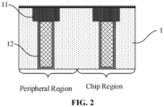
- the method may include: forming a bottom-layer dielectric layer 1 on the peripheral region and the chip region of the substrate, as shown in FIG. 2 .
- the bottom-layer dielectric layer 1 may be formed on the substrate, as shown in FIG. 2 , a bottom-layer metal layer 11 and an interconnection structure 12 are formed in the bottom-layer dielectric layer 1.
- a through hole is respectively formed in the peripheral region and the chip region of the bottom-layer dielectric layer 1, and the interconnection structure 12 and the bottom-layer metal layer 11 are stacked sequentially from bottom to top in the through hole.
- the interconnection structure 12 may be a single-layer structure, a stacked-layer structure or other structure, but the interconnection structure 12 in this embodiment is not limited thereto.
- a material of the interconnection structure 12 may comprise one or more of titanium, titanium nitride, or tungsten, etc. This embodiment does not limit the material of the interconnection structure 12.
- the interconnection structure 12 includes a conductive metal and a barrier layer, wherein the conductive metal may include, but is not limited to, tungsten, ruthenium, and the like, and the barrier layer may include, but is not limited to, titanium nitride, titanium, and the like.
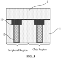
- Step S2 may include: forming a first dielectric layer 2 on the peripheral region and the chip region of the bottom-layer dielectric layer 1, as shown in FIG. 3 .
- Step S3 may include following steps:
- the width of the first opening 201 is the same as that of the fourth opening 204, and the width of the second opening 202 is the same as that of the fifth opening 205.
- an opening depth of the first opening 201 is the same as that of the fourth opening 204, and an opening depth of the second opening 202 is the same as that of the fifth opening 205.
- the opening depth of the first opening 201 is greater than that of the second opening 202, and the opening depth of the second opening 202 is greater than that of the third opening 203.
- the width of the first opening 201 is less than that of the second opening 202
- the width of the second opening 202 is less than that of the third opening 203
- the width of the fourth opening 204 is less than that of the fifth opening 205.
- a total depth of the first opening 201, the second opening 202 and the third opening 203 is the same as a total depth of the fourth opening 204 and the fifth opening 205.
- the electrically conductive material in the first opening 201 is the first subportion 211
- the electrically conductive material in the second opening 202 is the second subportion 212
- the electrically conductive material in the third opening 203 is the third subportion 213
- the electrically conductive material in the fourth opening 204 is the fourth subportion 224
- the electrically conductive material in the fifth opening 205 is the fifth subportion 225.
- the material of the protective structure 21 may include, but is not limited to, copper.
- the electrically conductive material may be copper, and an initial copper layer is formed simultaneously, by means of electroplating, in the first opening 201, the second opening 202, the third opening 203, the fourth opening 204, the fifth opening 205, and the first dielectric layer 2.
- the initial copper layer above the first dielectric layer 2 is removed by means of chemical mechanical grinding to form the protective structure 21 and the functional structure 22 respectively. as shown in FIG. 8 .
- the protective structure 21 may be formed separately in a copper-metal interconnection layer to enhance the protective effect of a copper-metal protection ring while saving production costs.
- the first dielectric layer 2 formed is a single-layer structure
- the protective structure 21 formed includes N subportions stacked sequentially, wherein N is an integer greater than 3.
- the first dielectric layer 2 may be a single-layer structure or a stacked-layer structure, and the structure of the first dielectric layer 2 in this embodiment is not limited thereto.
- the first dielectric layer 2 may be a silicon nitride layer and a silicon oxide layer stacked sequentially from bottom to top, and the protective structure 21 formed is positioned in the silicon oxide layer.
- the semiconductor structure formed by means of the method for manufacturing g a semiconductor structure provided in the above embodiment has more subportions, which increases its interception area and further enhances the protection of this structure for the chip.
- widths of the N subportions stacked in sequence are sequentially increased.
- the semiconductor structure formed by means of the method for manufacturing a semiconductor structure provided in the above embodiment has N subportions stacked in sequence, and the widths of the N subportions are sequentially increased, to ensure the structure to be more stable.
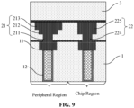
- the method may also include: S4: forming a second dielectric layer 3 on the first dielectric layer 2, as shown in FIG. 9 .
- the second dielectric layer 3 is a single-layer structure. In other embodiments, the second dielectric layer 3 may also be a stacked-layer structure. This embodiment does not limit the structure and arrangement of the second dielectric layer 3. In one embodiment, the second dielectric layer 3 may include one or more of a silicon nitride layer, a silicon oxide layer, and so on. This embodiment does not limit the material of the second dielectric layer 3. In some embodiments, in one embodiment, the second dielectric layer 3 may be the silicon nitride layer and the silicon oxide layer stacked sequentially from bottom to top.
- Step S4 the method may further comprise:
- the method may further include: S7: forming a top-layer interconnection structure 31 in the sixth opening 306 and the seventh opening 307, as shown in FIG. 11 .
- the top-layer interconnection structure 31 may be a single-layer structure, a stacked-layer structure, or other structure, and this embodiment does not limit the structure and arrangement of the top-layer interconnection structure 31.
- a material of the top-layer interconnection structure 31 may include one or more of aluminum, titanium, titanium nitride, or tungsten, etc. However, this embodiment does not limit the material of the top-layer interconnection structure 31.
- the top-layer interconnection structure 31 includes a titanium layer and a tungsten layer stacked sequentially from bottom to top.
- the method may further comprise: S8: forming a top-layer metal material layer 4 on the second dielectric layer 3, as shown in FIG. 12 .
- the top-layer metal material layer 4 formed is a single-layer structure or a stacked-layer structure, and this embodiment does not limit the structure and arrangement of the top-layer metal material layer 4.
- the top-layer metal material layer 4 may comprise a stacked-layer structure where the titanium layer and the aluminum layer are alternately stacked in sequence or a stacked-layer structure where the titanium nitride layer and the aluminum layer are alternately stacked in sequence, and a bottom layer and a top layer of the top-layer metal material layer are both the titanium layers or the titanium nitride layers.
- the method may further comprise: S9: etching the top-layer metal material layer 4 to form a top-layer metal layer 41 and expose a portion of the second dielectric layer 3, as shown in FIG. 13 .
- the method may further comprise: S10: forming a top-layer dielectric layer 5 over the second dielectric layer 3 and the top-layer metal layer 41, as shown in FIG. 14 .
- the top-layer dielectric layer 5 formed may be a single-layer structure or a stacked-layer structure, and this embodiment does not limit the structure of the top-layer dielectric layer 5.
- the top-layer dielectric layer 5 may be a silicon oxide layer and a silicon nitride layer stacked sequentially from bottom to top.
- steps in the flow diagrams of FIG. 1 and FIG. 4 are shown sequentially as indicated by the arrows, these steps are not necessarily performed sequentially in the order indicated by the arrows. It should be understood that unless expressly stated herein, the execution of these steps is not strictly limited in sequence, and these steps may be performed in other orders. Moreover, at least some of the steps in FIG. 1 and FIG. 4 may include a plurality of steps or a plurality of stages, which are not necessarily performed at the same moment, but may be executed at different moments, and the order of execution of these steps or stages is not necessarily performed sequentially, but may be performed alternately or alternately with at least a portion of the steps or stages of other steps or other steps.
- the present disclosure provides a semiconductor structure, comprising:
- the protective structure 21 comprises a first subportion 211, a second subportion 212 and a third subportion 213 stacked in sequence.
- the functional structure 22 comprises a fourth subportion 224 and a fifth subportion 225 stacked in sequence.
- a total height of the first subportion 211, the second subportion 212 and the third subportion 213 is equal to a total height of the fourth subportion 224 and the fifth subportion 225.
- the semiconductor structure provided by the above embodiment has a more stable structure, has a larger interception area, and provides better protection to a chip.
- the substrate may include, but is not limited to, a silicon substrate.
- the substrate may also be a gallium nitride substrate, an indium phosphide substrate, or a sapphire substrate, etc.
- the bottom-layer dielectric layer 1 is formed on the substrate, the first dielectric layer 2 is formed on the peripheral region and the chip region of the bottom-layer dielectric layer 1, and the bottom-layer metal layer 11 and the interconnection structure 12 are formed in the bottom-layer dielectric layer 1.
- a through hole is respectively formed in the peripheral region and the chip region of the bottom-layer dielectric layer 1, and the interconnection structure 12 and the bottom-layer metal layer 11 are stacked sequentially from bottom to top in the through hole.
- the interconnection structure 12 may be a single-layer structure or a stacked-layer structure, and this embodiment does not limit the structure of the interconnection structure 12.
- a material of the interconnection structure 12 may include one or more of titanium, titanium nitride, or tungsten, etc. This embodiment does not limit the material of the interconnection structure 12.
- the interconnection structure 12 comprises a conductive metal and a barrier layer, wherein the conductive metal comprises tungsten, ruthenium, and the like, and the barrier layer comprises titanium nitride, titanium, and the like.
- the first dielectric layer 2 is a single-layer structure. In other embodiments, the first dielectric layer 2 may also be a stacked-layer structure. This embodiment does not limit the structure and arrangement of the first dielectric layer 2. In one embodiment, the first dielectric layer 2 may include one or more of a silicon nitride layer, a silicon oxide layer, and so on. This embodiment does not limit the material of the first dielectric layer 2. In some embodiments, in one embodiment, the first dielectric layer 2 may be the silicon nitride layer and the silicon oxide layer stacked sequentially from bottom to top, and the protective structure 21 formed is positioned in the silicon oxide layer.
- the width of the second subportion 212 is greater than that of the first subportion 211, and the width of the third subportion 213 is greater than that of the second subportion 212.
- the width of the first subportion 211 is the same as that of the fourth subportion 224, and the width of the second subportion 212 is the same as that of the fifth subportion 225.
- first subportion 211, the second subportion 212, and the third subportion 213 are integrally formed.
- the fourth subportion 224 and the fifth subportion 225 are integrally formed.
- the protective structure 21 includes N subportions stacked sequentially, wherein N is an integer greater than 3.
- the semiconductor structure provided in the above embodiment has more subportions, which further increases the interception area and further enhances the protection of this structure for the chip.
- widths of the N subportions stacked in sequence are sequentially increased.
- the semiconductor structure provided in the above embodiment has N subportions stacked in sequence, and the widths of the N subportions are sequentially increased, to ensure the structure to be more stable.
- the first subportion 211, the second subportion 212, and the third subportion 213 are all annular wall structures.
- the fourth subportion 224 is a conductive plug structure, and the fifth subportion 225 is a conductive wire structure.
- the semiconductor structure further comprises a bottom metal layer positioned below the protective structure 21.
- the material of the bottom-layer metal layer may include, but is not limited to, tungsten.
- the semiconductor structure further comprises: a second dielectric layer 3 arranged on the first dielectric layer 2.
- the second dielectric layer 3 is a single-layer structure. In other embodiments, the first dielectric layer 2 may also be a stacked-layer structure. This embodiment does not limit the structure and arrangement of the second dielectric layer 3. In one embodiment, the second dielectric layer 3 may include one or more of a silicon nitride layer, a silicon oxide layer, and so on. This embodiment does not limit the material of the second dielectric layer 3. In some embodiments, in one embodiment, the second dielectric layer 3 may be the silicon nitride layer and the silicon oxide layer stacked sequentially from bottom to top.
- the semiconductor structure further comprises:
- the top-layer interconnection structure 31 may be a single-layer structure, a stacked-layer structure, or other structure, and this embodiment does not limit the structure and arrangement of the top-layer interconnection structure 31.
- a material of the top-layer interconnection structure 31 may include one or more of titanium, titanium nitride, or tungsten, etc. However, this embodiment does not limit the material of the top-layer interconnection structure 31.
- the top-layer interconnection structure 31 includes a titanium layer and a tungsten layer stacked sequentially from bottom to top.
- the semiconductor structure further comprises: a top-layer metal layer 41 arranged on an upper surface of the second dielectric layer 3.
- the top-layer metal layer 41 is a single-layer structure or a stacked-layer structure, and this embodiment does not limit the structure and arrangement of the top-layer metal layer 41.
- the top-layer metal material layer 41 may comprise a stacked-layer structure where the titanium layer and the aluminum layer are alternately stacked in sequence or a stacked-layer structure where the titanium nitride layer and the aluminum layer are alternately stacked in sequence, and a bottom layer and a top layer of the top-layer metal material layer are both the titanium layers or the titanium nitride layers.
- the semiconductor structure further comprises: a top-layer dielectric layer 5 arranged on the upper surface of the second dielectric layer 3 and the upper surface of the top-layer metal layer 41.
- the top-layer dielectric layer 5 formed may be a single-layer structure or a stacked-layer structure, and this embodiment does not limit the structure of the top-layer dielectric layer 5.
- the top-layer dielectric layer 5 may be a silicon oxide layer and a silicon nitride layer stacked sequentially from bottom to top.
Landscapes
- Internal Circuitry In Semiconductor Integrated Circuit Devices (AREA)
Abstract
Description
- This application claims priority to
Chinese Patent Application No. 202110315842.6 titled "SEMICONDUCTOR STRUCTURE AND MANUFACTURING METHOD THEREOF" and filed to the China National Intellectual Property Administration on March 24, 2021 - The present disclosure relates to the field of semiconductor manufacturing technology, and more particularly, to a semiconductor structure and a manufacturing method thereof.
- When a wafer is diced, a dicing mode of a dicing street may generate a certain mechanical stress on front and back surfaces of the wafer, which may cause chippings at an edge of a chip. The problem of chippings may reduce a mechanical strength of the chip, and an initial chip edge crack may be further spread in later packaging process or in the use of chip products, which may likely cause cracking of the chip, thus leading to failure of electrical properties of the chip. To protect internal circuits of the chip, prevent scratch damage, and improve reliability of the chip, a semiconductor structure such as a seal ring generally is designed at the periphery of the chip. Moreover, the seal ring structure also is capable of resisting gas and liquid erosion, which can prevent water vapor or other chemical contamination sources from permeating the chip to avoid causing damage to the chip.
- At present, as sizes of semiconductor devices continue to decrease, roles of the seal ring at the periphery of the chip are becoming more and more important. However, the existing sealing rings are unable to provide better protection to the chip due to their poor stability and smaller interception area, and can no longer meet the requirements for protection of the chip.
- According to various embodiments of the present disclosure, a semiconductor structure and a manufacturing method thereof are provided.
- The present disclosure provides a semiconductor structure, comprising:
- a substrate comprising a peripheral region and a chip region;
- a first dielectric layer positioned on the peripheral region and the chip region of the substrate; and
- a protective structure and a functional structure respectively positioned in the first dielectric layer on the peripheral region and in the first dielectric layer on the chip region.
- The protective structure comprises a first subportion, a second subportion and a third subportion stacked in sequence. The functional structure comprises a fourth subportion and a fifth subportion stacked in sequence. A total height of the first subportion, the second subportion and the third subportion is equal to a total height of the fourth subportion and the fifth subportion.
- The present disclosure also provides a method for manufacturing a semiconductor structure, wherein the method includes following steps:
- providing a substrate comprising a peripheral region and a chip region;
- forming a first dielectric layer on the peripheral region and the chip region of the substrate; and
- forming a protective structure and a functional structure respectively in the first dielectric layer on the peripheral region and in the first dielectric layer on the chip region.
- The protective structure comprises a first subportion, a second subportion and a third subportion stacked in sequence. The functional structure comprises a fourth subportion and a fifth subportion stacked in sequence. A total height of the first subportion, the second subportion and the third subportion is equal to a total height of the fourth subportion and the fifth subportion.
- The semiconductor structure provided by the embodiments of the present disclosure has a more stable structure, has a larger interception area, and provides better protection to a chip.
- The semiconductor structure formed by means of the method for manufacturing a semiconductor structure provided in the embodiments of the present disclosure has a more stable structure, has a larger interception area, provides better protection to the chip, and has a simpler technological process.
- To describe the technical solutions in the embodiments of the present disclosure or the existing technologies more clearly, the accompanying drawings required for describing the embodiments or the existing technologies will be briefly introduced below. Apparently, the accompanying drawings in the following description are merely some embodiments of the present disclosure. To those of ordinary skills in the art, other accompanying drawings may also be derived from these accompanying drawings without creative efforts.
-
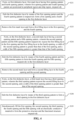
FIG. 1 is a flow diagram of a method for manufacturing a semiconductor structure according to one embodiment of the present disclosure; -
FIG. 2 is a schematic cross-sectional view of a bottom-layer dielectric layer according to one embodiment of the present disclosure; -
FIG. 3 is a schematic cross-sectional view of a structure obtained in Step S2 of a method for manufacturing a semiconductor structure according to one embodiment of the present disclosure; -
FIG. 4 is a flow diagram of Step S3 in a method for manufacturing a semiconductor structure according to one embodiment of the present disclosure; -
FIG. 5 is a schematic cross-sectional view of a structure obtained in Step S32 of a method for manufacturing a semiconductor structure according to one embodiment of the present disclosure; -
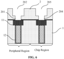
FIG. 6 is a schematic cross-sectional view of a structure obtained in Step S35 of a method for manufacturing a semiconductor structure according to one embodiment of the present disclosure; -
FIG. 7 is a schematic cross-sectional view of a structure obtained in Step S38 of a method for manufacturing a semiconductor structure according to one embodiment of the present disclosure; -
FIG. 8 is a schematic cross-sectional view of a structure obtained in Step S3 of a method for manufacturing a semiconductor structure according to one embodiment of the present disclosure, and also is a schematic diagram of a semiconductor structure according to one embodiment of the present disclosure; -
FIG. 9 is a schematic cross-sectional view of a structure obtained in Step S4 of a method for manufacturing a semiconductor structure according to one embodiment of the present disclosure; -
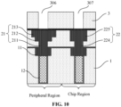
FIG. 10 is a schematic cross-sectional view of a structure obtained in Step S6 of a method for manufacturing a semiconductor structure according to one embodiment of the present disclosure; -
FIG. 11 is a schematic cross-sectional view of a structure obtained in Step S7 of a method for manufacturing a semiconductor structure according to one embodiment of the present disclosure; -
FIG. 12 is a schematic cross-sectional view of a structure obtained in Step S8 of a method for manufacturing a semiconductor structure according to one embodiment of the present disclosure; -
FIG. 13 is a schematic cross-sectional view of a structure obtained in Step S9 of a method for manufacturing a semiconductor structure according to one embodiment of the present disclosure; and -
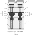
FIG. 14 is a schematic cross-sectional view of a structure obtained in Step S10 of a method for manufacturing a semiconductor structure according to one embodiment of the present disclosure, and also is a schematic diagram of a semiconductor structure according to one embodiment of the present disclosure. - For ease of understanding the present disclosure, the present disclosure will be described more fully hereinafter with reference to the accompanying drawings. Some embodiments of the present disclosure are provided in the accompanying drawings. The present disclosure may, however, be embodied in many different forms and should not be limited to the embodiments set forth herein. Rather, these embodiments are provided so that the present disclosure will be more thorough and complete.
- Unless otherwise defined, all technical and scientific terms employed herein have the same meaning as commonly understood by one of ordinary skill in the art to which the present disclosure belongs. The terms employed in the specification of the present disclosure are merely for the purpose of describing some embodiments and are not intended for limiting the present disclosure.
- It should be understood that when an element or layer is referred to as being "on", "adjacent to", "connected to" or "coupled to" other elements or layers, it may be directly on, adjacent to, connected or coupled to the other elements or layers, or intervening elements or layers may be present. In contrast, when an element is referred to as being "directly on", "directly adjacent to", "directly connected to" or "directly coupled to" other elements or layers, there are no intervening elements or layers present. It should be understood that although the terms first, second, third, etc. may be employed to describe various elements, components, regions, layers, doping types and/or sections, these elements, components, regions, layers, doping types and/or sections should not be limited by these terms. These terms are only employed to distinguish one element, component, region, layer, doping type, or section from another element, component, region, layer, doping type, or section. Thus, without departing from the teachings of the present disclosure, a first element, component, region, layer, doping type or portion discussed below may be represented as a second element, component, region, layer or portion. For example, a first doping type may be a second doping type, and similarly, the second doping type may be the first doping type. Furthermore, the first doping type and the second doping type may be different doping types. For example, the first doping type may be a P type and the second doping type may be an N type, or the first doping type may be the N type and the second doping type may be the P type.
- Spatially relative terms such as "below", "under", "lower", "beneath", "above", "upper" and the like may be used herein to describe relationships between one element or feature as shown in the figures and another element(s) or feature(s). It should be understood that the spatially relative terms may be intended to encompass different orientations of a device in use or operation in addition to the orientation depicted in the figures. For example, if the device in the figures is turned over, elements or features described as "under", "beneath" or "below" other elements would then be oriented "above" the other elements or features. Thus, the example term "under", "below" or "beneath" may encompass both an orientation of above and below. In addition, the device may also be otherwise oriented (for example, rotated 90 degrees or at other orientations) and the spatially descriptors used herein should be interpreted accordingly.
- As used herein, the singular forms of "a", "one" and "said/the" are also intended to include plural forms, unless the context clearly indicates otherwise. It should also be understood that the terms "comprising" and/or "including", when used in this specification, may determine the presence of the described features, integers, steps, operations, elements and/or components, but do not preclude the presence or addition of one or more other features, integers, steps, operations, elements, components, and/or groups thereof. Meanwhile, as used herein, the term "and/or" includes any and all combinations of related listed items.
- Embodiments of the present disclosure are described herein with reference to cross-sectional illustrations serving as schematic illustrations of embodiments (and intermediate structures) of the present disclosure. As such, variations from the shapes of the illustrations as a result, for example, of manufacturing techniques and/or tolerances, may be expected. Thus, embodiments of the present disclosure should not be construed as being limited to particular shapes of regions illustrated herein but may include deviations in shapes that result, for example, from manufacturing technologies. Thus, regions illustrated in the figures are schematic in nature and their shapes do not necessarily illustrate the actual shape of a region of the device and do not limit the scope of the present disclosure.
- With reference to
FIG. 1 , an embodiment of the present disclosure provides a method for manufacturing a semiconductor structure, wherein the method includes following steps: - S 1: providing a substrate (not shown in the figure), which includes a peripheral region and a chip region;
- S2: forming a first
dielectric layer 2 on the peripheral region and the chip region of the substrate; and - S3: forming a
protective structure 21 and afunctional structure 22 in the firstdielectric layer 2 on the peripheral region and in the firstdielectric layer 2 on the chip region, respectively. - The
protective structure 21 comprises afirst subportion 211, asecond subportion 212 and athird subportion 213 stacked in sequence. Thefunctional structure 22 comprises afourth subportion 224 and afifth subportion 225 stacked in sequence. A total height of thefirst subportion 211, thesecond subportion 212 and thethird subportion 213 is equal to a total height of thefourth subportion 224 and thefifth subportion 225. - The semiconductor structure formed by means of the method for manufacturing a semiconductor structure provided in the above embodiment has a more stable structure, has a larger interception area, provides better protection to the chip, and has a simpler technological process.
- In one embodiment, the substrate may include, but is not limited to, a silicon substrate. In other embodiments, the substrate may also be a gallium nitride substrate, an indium phosphide substrate, or a sapphire substrate, etc.
- In one embodiment, before Step S2, the method may include:
forming a bottom-layer dielectric layer 1 on the peripheral region and the chip region of the substrate, as shown inFIG. 2 . - It is to be noted that the bottom-
layer dielectric layer 1 may be formed on the substrate, as shown inFIG. 2 , a bottom-layer metal layer 11 and aninterconnection structure 12 are formed in the bottom-layer dielectric layer 1. In some embodiments, in one embodiment, a through hole is respectively formed in the peripheral region and the chip region of the bottom-layer dielectric layer 1, and theinterconnection structure 12 and the bottom-layer metal layer 11 are stacked sequentially from bottom to top in the through hole. - In one embodiment, the
interconnection structure 12 may be a single-layer structure, a stacked-layer structure or other structure, but theinterconnection structure 12 in this embodiment is not limited thereto. In one embodiment, a material of theinterconnection structure 12 may comprise one or more of titanium, titanium nitride, or tungsten, etc. This embodiment does not limit the material of theinterconnection structure 12. In one embodiment, theinterconnection structure 12 includes a conductive metal and a barrier layer, wherein the conductive metal may include, but is not limited to, tungsten, ruthenium, and the like, and the barrier layer may include, but is not limited to, titanium nitride, titanium, and the like. - In the above embodiment, Step S2 may include:
forming a firstdielectric layer 2 on the peripheral region and the chip region of the bottom-layer dielectric layer 1, as shown inFIG. 3 . - For Step S3, as shown in
FIG. 4 , in one embodiment, Step S3 may include following steps: - S31: forming, on the first
dielectric layer 2, a first mask layer having a first opening pattern and a fourth opening pattern, wherein the first opening pattern and the fourth opening pattern are positioned in the peripheral region and the chip region, respectively; - S32: etching the first
dielectric layer 2 by means of the first opening pattern and the fourth opening pattern to respectively form afirst opening 201 and afourth opening 204 in the firstdielectric layer 2, as shown inFIG. 5 ; - S33: removing the first mask layer and forming a first filling layer in the
first opening 201 and thefourth opening 204; - S34: forming, on the first
dielectric layer 2, a second mask layer having a second opening pattern and a fifth opening pattern, wherein the second opening pattern and the fifth opening pattern respectively expose the first filling layer in thefirst opening 201 and the first filling layer in thefourth opening 204, a width of the second opening pattern is greater than that of thefirst opening 201, and a width of the fifth opening pattern is greater than that of thefourth opening 204; - S3 5: etching the first
dielectric layer 2 by means of the second opening pattern and the fifth opening pattern to form thesecond opening 202 and thefifth opening 205 respectively in the firstdielectric layer 2, as shown inFIG. 6 ; - S36: removing the second mask layer and forming a second filling layer in the
second opening 202 and thefifth opening 205; - S37: forming, on the first
dielectric layer 2, a third mask layer having a third opening pattern, wherein the third opening pattern exposes the second filling layer in thesecond opening 202, and a width of the third opening pattern is greater than that of thesecond opening 202; - S38: etching the first
dielectric layer 2 by means of the third opening pattern to form athird opening 203 in the firstdielectric layer 2, as shown inFIG. 7 ; and - S39: simultaneously filling the
first opening 201, thesecond opening 202, thethird opening 203, thefourth opening 204 and thefifth opening 205 with an electrically conductive material to form theprotective structure 21 and thefunctional structure 22 respectively, as shown inFIG. 8 . - In one embodiment, the width of the
first opening 201 is the same as that of thefourth opening 204, and the width of thesecond opening 202 is the same as that of thefifth opening 205. - Further, in one embodiment, an opening depth of the
first opening 201 is the same as that of thefourth opening 204, and an opening depth of thesecond opening 202 is the same as that of thefifth opening 205. - In one embodiment, the opening depth of the
first opening 201 is greater than that of thesecond opening 202, and the opening depth of thesecond opening 202 is greater than that of thethird opening 203. - In one embodiment, the width of the
first opening 201 is less than that of thesecond opening 202, the width of thesecond opening 202 is less than that of thethird opening 203, and the width of thefourth opening 204 is less than that of thefifth opening 205. - In one embodiment, a total depth of the
first opening 201, thesecond opening 202 and thethird opening 203 is the same as a total depth of thefourth opening 204 and thefifth opening 205. - The electrically conductive material in the
first opening 201 is thefirst subportion 211, the electrically conductive material in thesecond opening 202 is thesecond subportion 212, the electrically conductive material in thethird opening 203 is thethird subportion 213, the electrically conductive material in thefourth opening 204 is thefourth subportion 224, and the electrically conductive material in thefifth opening 205 is thefifth subportion 225. - In some embodiments, in one embodiment, the material of the
protective structure 21 may include, but is not limited to, copper. - In some embodiments, the electrically conductive material may be copper, and an initial copper layer is formed simultaneously, by means of electroplating, in the
first opening 201, thesecond opening 202, thethird opening 203, thefourth opening 204, thefifth opening 205, and the firstdielectric layer 2. Next, the initial copper layer above the firstdielectric layer 2 is removed by means of chemical mechanical grinding to form theprotective structure 21 and thefunctional structure 22 respectively. as shown inFIG. 8 . Theprotective structure 21 may be formed separately in a copper-metal interconnection layer to enhance the protective effect of a copper-metal protection ring while saving production costs. - In one embodiment, the first
dielectric layer 2 formed is a single-layer structure, and theprotective structure 21 formed includes N subportions stacked sequentially, wherein N is an integer greater than 3. - In one embodiment, the first
dielectric layer 2 may be a single-layer structure or a stacked-layer structure, and the structure of the firstdielectric layer 2 in this embodiment is not limited thereto. In some embodiments, in one embodiment, the firstdielectric layer 2 may be a silicon nitride layer and a silicon oxide layer stacked sequentially from bottom to top, and theprotective structure 21 formed is positioned in the silicon oxide layer. - The semiconductor structure formed by means of the method for manufacturing g a semiconductor structure provided in the above embodiment has more subportions, which increases its interception area and further enhances the protection of this structure for the chip.
- In one embodiment, widths of the N subportions stacked in sequence are sequentially increased.
- The semiconductor structure formed by means of the method for manufacturing a semiconductor structure provided in the above embodiment has N subportions stacked in sequence, and the widths of the N subportions are sequentially increased, to ensure the structure to be more stable.
- In one embodiment, after Step S3, the method may also include:
S4: forming asecond dielectric layer 3 on the firstdielectric layer 2, as shown inFIG. 9 . - In one embodiment, the
second dielectric layer 3 is a single-layer structure. In other embodiments, thesecond dielectric layer 3 may also be a stacked-layer structure. This embodiment does not limit the structure and arrangement of thesecond dielectric layer 3. In one embodiment, thesecond dielectric layer 3 may include one or more of a silicon nitride layer, a silicon oxide layer, and so on. This embodiment does not limit the material of thesecond dielectric layer 3. In some embodiments, in one embodiment, thesecond dielectric layer 3 may be the silicon nitride layer and the silicon oxide layer stacked sequentially from bottom to top. - In one embodiment, after Step S4, the method may further comprise:
- S5: forming, on the
second dielectric layer 3, a fourth mask layer having a sixth opening pattern and a seventh opening pattern, wherein the sixth opening pattern and the seventh opening pattern are positioned in the peripheral region and the chip region, respectively; and - S6: etching the
second dielectric layer 3 by means of the sixth opening pattern and the seventh opening pattern to form asixth opening 306 and aseventh opening 307 respectively in thesecond dielectric layer 3, as shown inFIG. 10 , wherein thesixth opening 306 and theseventh opening 307 are positioned in the peripheral region and the chip region, respectively. - In one embodiment, after Step S6, the method may further include:
S7: forming a top-layer interconnection structure 31 in thesixth opening 306 and theseventh opening 307, as shown inFIG. 11 . - In one embodiment, the top-
layer interconnection structure 31 may be a single-layer structure, a stacked-layer structure, or other structure, and this embodiment does not limit the structure and arrangement of the top-layer interconnection structure 31. In one embodiment, a material of the top-layer interconnection structure 31 may include one or more of aluminum, titanium, titanium nitride, or tungsten, etc. However, this embodiment does not limit the material of the top-layer interconnection structure 31. In one embodiment, the top-layer interconnection structure 31 includes a titanium layer and a tungsten layer stacked sequentially from bottom to top. - In one embodiment, after Step S7, the method may further comprise:
S8: forming a top-layermetal material layer 4 on thesecond dielectric layer 3, as shown inFIG. 12 . - In one embodiment, the top-layer
metal material layer 4 formed is a single-layer structure or a stacked-layer structure, and this embodiment does not limit the structure and arrangement of the top-layermetal material layer 4. In one embodiment, the top-layermetal material layer 4 may comprise a stacked-layer structure where the titanium layer and the aluminum layer are alternately stacked in sequence or a stacked-layer structure where the titanium nitride layer and the aluminum layer are alternately stacked in sequence, and a bottom layer and a top layer of the top-layer metal material layer are both the titanium layers or the titanium nitride layers. - In one embodiment, after Step S8, the method may further comprise:
S9: etching the top-layermetal material layer 4 to form a top-layer metal layer 41 and expose a portion of thesecond dielectric layer 3, as shown inFIG. 13 . - In one embodiment, after Step S9, the method may further comprise:
S10: forming a top-layer dielectric layer 5 over thesecond dielectric layer 3 and the top-layer metal layer 41, as shown inFIG. 14 . - In one embodiment, the top-
layer dielectric layer 5 formed may be a single-layer structure or a stacked-layer structure, and this embodiment does not limit the structure of the top-layer dielectric layer 5. In some embodiments, in one embodiment, the top-layer dielectric layer 5 may be a silicon oxide layer and a silicon nitride layer stacked sequentially from bottom to top. - It should be understood that although the steps in the flow diagrams of
FIG. 1 andFIG. 4 are shown sequentially as indicated by the arrows, these steps are not necessarily performed sequentially in the order indicated by the arrows. It should be understood that unless expressly stated herein, the execution of these steps is not strictly limited in sequence, and these steps may be performed in other orders. Moreover, at least some of the steps inFIG. 1 andFIG. 4 may include a plurality of steps or a plurality of stages, which are not necessarily performed at the same moment, but may be executed at different moments, and the order of execution of these steps or stages is not necessarily performed sequentially, but may be performed alternately or alternately with at least a portion of the steps or stages of other steps or other steps. - With continued reference to
FIG. 8 , the present disclosure provides a semiconductor structure, comprising: - a substrate, the substrate comprising a peripheral region and a chip region;
- a first
dielectric layer 2 arranged on the peripheral region and the chip region of the substrate; and - a
protective structure 21 and afunctional structure 22 in the firstdielectric layer 2 on the peripheral region and in the firstdielectric layer 2 on the chip region, respectively. - The
protective structure 21 comprises afirst subportion 211, asecond subportion 212 and athird subportion 213 stacked in sequence. Thefunctional structure 22 comprises afourth subportion 224 and afifth subportion 225 stacked in sequence. A total height of thefirst subportion 211, thesecond subportion 212 and thethird subportion 213 is equal to a total height of thefourth subportion 224 and thefifth subportion 225. - The semiconductor structure provided by the above embodiment has a more stable structure, has a larger interception area, and provides better protection to a chip.
- In one embodiment, the substrate may include, but is not limited to, a silicon substrate. In other embodiments, the substrate may also be a gallium nitride substrate, an indium phosphide substrate, or a sapphire substrate, etc.
- In one embodiment, the bottom-
layer dielectric layer 1 is formed on the substrate, the firstdielectric layer 2 is formed on the peripheral region and the chip region of the bottom-layer dielectric layer 1, and the bottom-layer metal layer 11 and theinterconnection structure 12 are formed in the bottom-layer dielectric layer 1. In some embodiments, in one embodiment, a through hole is respectively formed in the peripheral region and the chip region of the bottom-layer dielectric layer 1, and theinterconnection structure 12 and the bottom-layer metal layer 11 are stacked sequentially from bottom to top in the through hole. - In one embodiment, the
interconnection structure 12 may be a single-layer structure or a stacked-layer structure, and this embodiment does not limit the structure of theinterconnection structure 12. In one embodiment, a material of theinterconnection structure 12 may include one or more of titanium, titanium nitride, or tungsten, etc. This embodiment does not limit the material of theinterconnection structure 12. In one embodiment, theinterconnection structure 12 comprises a conductive metal and a barrier layer, wherein the conductive metal comprises tungsten, ruthenium, and the like, and the barrier layer comprises titanium nitride, titanium, and the like. - In one embodiment, the first
dielectric layer 2 is a single-layer structure. In other embodiments, the firstdielectric layer 2 may also be a stacked-layer structure. This embodiment does not limit the structure and arrangement of the firstdielectric layer 2. In one embodiment, the firstdielectric layer 2 may include one or more of a silicon nitride layer, a silicon oxide layer, and so on. This embodiment does not limit the material of the firstdielectric layer 2. In some embodiments, in one embodiment, the firstdielectric layer 2 may be the silicon nitride layer and the silicon oxide layer stacked sequentially from bottom to top, and theprotective structure 21 formed is positioned in the silicon oxide layer. - In one embodiment, the width of the
second subportion 212 is greater than that of thefirst subportion 211, and the width of thethird subportion 213 is greater than that of thesecond subportion 212. - In one embodiment, the width of the
first subportion 211 is the same as that of thefourth subportion 224, and the width of thesecond subportion 212 is the same as that of thefifth subportion 225. - In one embodiment, the
first subportion 211, thesecond subportion 212, and thethird subportion 213 are integrally formed. Thefourth subportion 224 and thefifth subportion 225 are integrally formed. - In one embodiment, the
protective structure 21 includes N subportions stacked sequentially, wherein N is an integer greater than 3. - The semiconductor structure provided in the above embodiment has more subportions, which further increases the interception area and further enhances the protection of this structure for the chip.
- In one embodiment, widths of the N subportions stacked in sequence are sequentially increased.
- The semiconductor structure provided in the above embodiment has N subportions stacked in sequence, and the widths of the N subportions are sequentially increased, to ensure the structure to be more stable.
- In some embodiments, in one embodiment, the
first subportion 211, thesecond subportion 212, and thethird subportion 213 are all annular wall structures. Thefourth subportion 224 is a conductive plug structure, and thefifth subportion 225 is a conductive wire structure. - In one embodiment, the semiconductor structure further comprises a bottom metal layer positioned below the
protective structure 21. In some embodiments, the material of the bottom-layer metal layer may include, but is not limited to, tungsten. - With continued reference to
FIG. 9 , in one embodiment, the semiconductor structure further comprises:
asecond dielectric layer 3 arranged on the firstdielectric layer 2. - In one embodiment, the
second dielectric layer 3 is a single-layer structure. In other embodiments, the firstdielectric layer 2 may also be a stacked-layer structure. This embodiment does not limit the structure and arrangement of thesecond dielectric layer 3. In one embodiment, thesecond dielectric layer 3 may include one or more of a silicon nitride layer, a silicon oxide layer, and so on. This embodiment does not limit the material of thesecond dielectric layer 3. In some embodiments, in one embodiment, thesecond dielectric layer 3 may be the silicon nitride layer and the silicon oxide layer stacked sequentially from bottom to top. - Referring to
FIG. 11 , in one embodiment, the semiconductor structure further comprises: - a
sixth opening 306; - a
seventh opening 307, both thesixth opening 306 and theseventh opening 307 being positioned in thesecond dielectric layer 3 and positioned in the peripheral region and the chip region, respectively; and - a top-
layer interconnection structure 31 arranged in thesixth opening 306 and theseventh opening 307. - In one embodiment, the top-
layer interconnection structure 31 may be a single-layer structure, a stacked-layer structure, or other structure, and this embodiment does not limit the structure and arrangement of the top-layer interconnection structure 31. In one embodiment, a material of the top-layer interconnection structure 31 may include one or more of titanium, titanium nitride, or tungsten, etc. However, this embodiment does not limit the material of the top-layer interconnection structure 31. In one embodiment, the top-layer interconnection structure 31 includes a titanium layer and a tungsten layer stacked sequentially from bottom to top. - With continued reference to
FIG. 12 , in one embodiment, the semiconductor structure further comprises:
a top-layer metal layer 41 arranged on an upper surface of thesecond dielectric layer 3. - In one embodiment, the top-
layer metal layer 41 is a single-layer structure or a stacked-layer structure, and this embodiment does not limit the structure and arrangement of the top-layer metal layer 41. In one embodiment, the top-layermetal material layer 41 may comprise a stacked-layer structure where the titanium layer and the aluminum layer are alternately stacked in sequence or a stacked-layer structure where the titanium nitride layer and the aluminum layer are alternately stacked in sequence, and a bottom layer and a top layer of the top-layer metal material layer are both the titanium layers or the titanium nitride layers. - With continued reference to
FIG. 14 , in one embodiment, the semiconductor structure further comprises:
a top-layer dielectric layer 5 arranged on the upper surface of thesecond dielectric layer 3 and the upper surface of the top-layer metal layer 41. - In one embodiment, the top-
layer dielectric layer 5 formed may be a single-layer structure or a stacked-layer structure, and this embodiment does not limit the structure of the top-layer dielectric layer 5. In some embodiments, in one embodiment, the top-layer dielectric layer 5 may be a silicon oxide layer and a silicon nitride layer stacked sequentially from bottom to top. - Technical features of the above embodiments may be arbitrarily combined. For simplicity, all possible combinations of the technical features in the above embodiments are not described. However, as long as the combination of these technical features is not contradictory, it shall be deemed to be within the scope recorded in this specification.
- The above embodiments merely express a plurality of implementations of the present disclosure, and descriptions thereof are relatively concrete and detailed. However, these embodiments are not thus construed as limiting the patent scope of the present disclosure. It is to be pointed out that for persons of ordinary skill in the art, some modifications and improvements may be made under the premise of not departing from a conception of the present disclosure, which shall be regarded as falling within the scope of protection of the present disclosure. Thus, the scope of protection of the present disclosure shall be subject to the appended claims.
Claims (15)
- A semiconductor structure, comprising:a substrate, the substrate comprising a peripheral region and a chip region;a first dielectric layer positioned on the peripheral region and the chip region of the substrate; anda protective structure and a functional structure respectively positioned in the first dielectric layer on the peripheral region and in the first dielectric layer on the chip region;wherein the protective structure comprises a first subportion, a second subportion and a third subportion stacked in sequence, the functional structure comprising a fourth subportion and a fifth subportion stacked in sequence, a total height of the first subportion, the second subportion and the third subportion being equal to a total height of the fourth subportion and the fifth subportion.
- The semiconductor structure according to claim 1, whereina width of the second subportion is greater than that of the first subportion; anda width of the third subportion is greater than the width of the second subportion.
- The semiconductor structure according to claim 2, whereinthe width of the first subportion is equal to that of the fourth subportion; andthe width of the second subportion is equal to that of the fifth subportion.
- The semiconductor structure according to claim 1, whereinthe first subportion, the second subportion and the third subportion are integrally formed; andthe fourth subportion and the fifth subportion are integrally formed.
- The semiconductor structure according to claim 1, wherein
the first dielectric layer is a single-layer structure. - The semiconductor structure according to claim 1, wherein
the protective structure comprises N subportions stacked in sequence, the N being an integer greater than 3. - The semiconductor structure according to claim 6, wherein
widths of the N subportions stacked in sequence increase successively. - The semiconductor structure according to claim 1, whereinthe first subportion, the second subportion and the third subportion are all annular wall structures;the fourth subportion is a conductive plug structure; andthe fifth subportion is a conductive wire structure.
- The semiconductor structure according to claim 4, further comprising:a bottom metal layer positioned below the protective structure and a top-layer interconnection structure positioned above the protective structure, respectively; whereina material of the protective structure comprises copper, a material of the bottom metal layer comprising tungsten, and a material of the top-layer interconnection structure comprising tungsten or aluminum.
- A method for manufacturing a semiconductor structure, comprising:providing a substrate, the substrate comprising a peripheral region and a chip region;forming a first dielectric layer on the peripheral region and the chip region of the substrate; andforming a protective structure and a functional structure respectively in the first dielectric layer on the peripheral region and in the first dielectric layer on the chip region;wherein the protective structure comprises a first subportion, a second subportion and a third subportion stacked in sequence, the functional structure comprising a fourth subportion and a fifth subportion stacked in sequence, a total height of the first subportion, the second subportion and the third subportion being equal to a total height of the fourth subportion and the fifth subportion.
- The method for manufacturing a semiconductor structure according to claim 10, wherein the forming a protective structure and a functional structure respectively in the first dielectric layer on the peripheral region and in the first dielectric layer on the chip region comprises:forming, on the first dielectric layer, a first mask layer having a first opening pattern and a fourth opening pattern, the first opening pattern and the fourth opening pattern being positioned in the peripheral region and the chip region, respectively;etching the first dielectric layer by means of the first opening pattern and the fourth opening pattern to respectively form a first opening and a fourth opening in the first dielectric layer;removing the first mask layer and forming a first filling layer in the first opening and the fourth opening;forming, on the first dielectric layer, a second mask layer having a second opening pattern and a fifth opening pattern, the second opening pattern and the fifth opening pattern respectively exposing the first filling layer in the first opening and the first filling layer in the fourth opening, a width of the second opening pattern being greater than that of the first opening, and a width of the fifth opening pattern being greater than that of the fourth opening;etching the first dielectric layer by means of the second opening pattern and the fifth opening pattern to form a second opening and a fifth opening in the first dielectric layer, respectively;removing the second mask layer and forming a second filling layer in the second opening and the fifth opening;forming, on the first dielectric layer, a third mask layer having a third opening pattern, the third opening pattern exposing the second filling layer in the second opening, and a width of the third opening pattern being greater than that of the second opening;etching the first dielectric layer by means of the third opening pattern to form a third opening in the first dielectric layer; andsimultaneously filling the first opening, the second opening, the third opening, the fourth opening and the fifth opening with an electrically conductive material to form the protective structure and the functional structure, respectively.
- The method for manufacturing a semiconductor structure according to claim 11, whereinthe width of the first opening is equal to the width of the fourth opening; andthe width of the second opening is equal to that of the fifth opening.
- The method for manufacturing a semiconductor structure according to claim 12, whereinan opening depth of the first opening is equal to that of the fourth opening; andan opening depth of the second opening is equal to that of the fifth opening.
- The method for manufacturing a semiconductor structure according to claim 10, whereinthe first dielectric layer formed is a single-layer structure; andthe protective structure formed comprises N subportions stacked in sequence, the N being an integer greater than 3.
- The method for manufacturing a semiconductor structure according to claim 14, wherein
widths of the N subportions stacked in sequence increase successively.
Applications Claiming Priority (2)
| Application Number | Priority Date | Filing Date | Title |
|---|---|---|---|
| CN202110315842.6A CN113066763B (en) | 2021-03-24 | 2021-03-24 | Semiconductor structure and manufacturing method thereof |
| PCT/CN2021/111069 WO2022198878A1 (en) | 2021-03-24 | 2021-08-06 | Semiconductor structure and manufacturing method therefor |
Publications (3)
| Publication Number | Publication Date |
|---|---|
| EP4203002A1 true EP4203002A1 (en) | 2023-06-28 |
| EP4203002A4 EP4203002A4 (en) | 2024-05-22 |
| EP4203002B1 EP4203002B1 (en) | 2025-06-11 |
Family
ID=83364931
Family Applications (1)
| Application Number | Title | Priority Date | Filing Date |
|---|---|---|---|
| EP21932490.2A Active EP4203002B1 (en) | 2021-03-24 | 2021-08-06 | Semiconductor structure with a sealing ring and manufacturing method therefor |
Country Status (2)
| Country | Link |
|---|---|
| US (1) | US20220310484A1 (en) |
| EP (1) | EP4203002B1 (en) |
Families Citing this family (1)
| Publication number | Priority date | Publication date | Assignee | Title |
|---|---|---|---|---|
| US12165919B2 (en) * | 2021-01-19 | 2024-12-10 | Changxin Memory Technologies, Inc. | Semiconductor structure and manufacturing method thereof |
Family Cites Families (13)
| Publication number | Priority date | Publication date | Assignee | Title |
|---|---|---|---|---|
| JP4401874B2 (en) * | 2004-06-21 | 2010-01-20 | 株式会社ルネサステクノロジ | Semiconductor device |
| US8093719B1 (en) * | 2004-12-10 | 2012-01-10 | Cypress Semiconductor Corporation | Seal ring for preventing crack propagation in integrated circuit devices |
| KR100764741B1 (en) * | 2006-06-08 | 2007-10-08 | 삼성전자주식회사 | Semiconductor Device and Forming Method |
| KR101205161B1 (en) * | 2010-06-16 | 2012-11-27 | 에스케이하이닉스 주식회사 | Semiconductor device and method for forming the same |
| JP5947093B2 (en) * | 2012-04-25 | 2016-07-06 | ルネサスエレクトロニクス株式会社 | Manufacturing method of semiconductor integrated circuit device |
| US20170256506A1 (en) * | 2013-01-11 | 2017-09-07 | Renesas Electronics Corporation | Semiconductor device |
| US9368644B2 (en) * | 2013-12-20 | 2016-06-14 | Cypress Semiconductor Corporation | Gate formation memory by planarization |
| US9276057B2 (en) * | 2014-01-27 | 2016-03-01 | United Microelectronics Corp. | Capacitor structure and method of manufacturing the same |
| US9666520B2 (en) * | 2014-04-30 | 2017-05-30 | Taiwan Semiconductor Manufactuing Company, Ltd. | 3D stacked-chip package |
| CN105870069B (en) * | 2015-01-22 | 2018-07-24 | 中芯国际集成电路制造(上海)有限公司 | Protection structure for chip cutting process |
| DE102017118121B4 (en) * | 2017-08-09 | 2019-08-14 | Infineon Technologies Austria Ag | Semiconductor device and manufacturing method thereof |
| US11171098B2 (en) * | 2018-09-27 | 2021-11-09 | Taiwan Semiconductor Manufacturing Company, Ltd. | Package and manufacturing method thereof |
| US10840197B2 (en) * | 2018-10-30 | 2020-11-17 | Taiwan Semiconductor Manufacturing Company, Ltd. | Package structure and manufacturing method thereof |
-
2021
- 2021-08-06 EP EP21932490.2A patent/EP4203002B1/en active Active
- 2021-09-20 US US17/480,136 patent/US20220310484A1/en not_active Abandoned
Also Published As
| Publication number | Publication date |
|---|---|
| EP4203002B1 (en) | 2025-06-11 |
| US20220310484A1 (en) | 2022-09-29 |
| EP4203002A4 (en) | 2024-05-22 |
Similar Documents
| Publication | Publication Date | Title |
|---|---|---|
| CN102903687B (en) | Chip seal ring structure | |
| US11877442B2 (en) | Semiconductor memory device | |
| US7741715B2 (en) | Crack stop and moisture barrier | |
| US9245801B2 (en) | Crack stop barrier and method of manufacturing thereof | |
| US8008750B2 (en) | Crack stops for semiconductor devices | |
| CN102956618B (en) | With the integrated circuit of leakage current testing structure | |
| US20070069336A1 (en) | Seal ring corner design | |
| CN113380621B (en) | Semiconductor device and method for manufacturing the same | |
| CN106298694A (en) | A kind of semiconductor device and preparation method thereof and electronic installation | |
| EP4203002B1 (en) | Semiconductor structure with a sealing ring and manufacturing method therefor | |
| CN113066763B (en) | Semiconductor structure and manufacturing method thereof | |
| US20230140743A1 (en) | Sealing ring, stacked structure, and method for manufacturing sealing ring | |
| CN112885778B (en) | Semiconductor structure and manufacturing method thereof | |
| CN112687780B (en) | High-voltage light-emitting diode chip | |
| CN105789063A (en) | Semiconductor device and fabrication method thereof | |
| CN116093030B (en) | Sealing ring, stacking structure and manufacturing method of sealing ring | |
| US20250365995A1 (en) | Semiconductor device and preparation method therefor | |
| CN116230561A (en) | A power device terminal structure and manufacturing method | |
| CN110970313B (en) | Pad structure and preparation method of semiconductor structure | |
| CN111384001A (en) | Semiconductor device with a plurality of transistors | |
| US20250275251A1 (en) | Moat coverage with dielectric film for device passivation and singulation | |
| US12322671B2 (en) | Guard ring structure, semiconductor structure and manufacturing method | |
| CN222365583U (en) | Semiconductor components | |
| US20250349756A1 (en) | Semiconductor structure, semiconductor apparatus, and method for manufacturing semiconductor structure | |
| CN102184843A (en) | Chip cutting protection ring of diode based on groove MOSFET (metal-oxide-semiconductor field effect transistor) and manufacturing method thereof |
Legal Events
| Date | Code | Title | Description |
|---|---|---|---|
| STAA | Information on the status of an ep patent application or granted ep patent |
Free format text: STATUS: THE INTERNATIONAL PUBLICATION HAS BEEN MADE |
|
| PUAI | Public reference made under article 153(3) epc to a published international application that has entered the european phase |
Free format text: ORIGINAL CODE: 0009012 |
|
| STAA | Information on the status of an ep patent application or granted ep patent |
Free format text: STATUS: REQUEST FOR EXAMINATION WAS MADE |
|
| 17P | Request for examination filed |
Effective date: 20230320 |
|
| AK | Designated contracting states |
Kind code of ref document: A1 Designated state(s): AL AT BE BG CH CY CZ DE DK EE ES FI FR GB GR HR HU IE IS IT LI LT LU LV MC MK MT NL NO PL PT RO RS SE SI SK SM TR |
|
| REG | Reference to a national code |
Ref country code: DE Ref legal event code: R079 Ipc: H01L0023310000 Ref document number: 602021032293 Country of ref document: DE Free format text: PREVIOUS MAIN CLASS: H01L0023000000 |
|
| A4 | Supplementary search report drawn up and despatched |
Effective date: 20240418 |
|
| RIC1 | Information provided on ipc code assigned before grant |
Ipc: H01L 23/528 20060101ALN20240412BHEP Ipc: H01L 23/58 20060101ALI20240412BHEP Ipc: H01L 23/31 20060101AFI20240412BHEP |
|
| DAV | Request for validation of the european patent (deleted) | ||
| DAX | Request for extension of the european patent (deleted) | ||
| GRAP | Despatch of communication of intention to grant a patent |
Free format text: ORIGINAL CODE: EPIDOSNIGR1 |
|
| STAA | Information on the status of an ep patent application or granted ep patent |
Free format text: STATUS: GRANT OF PATENT IS INTENDED |
|
| RIC1 | Information provided on ipc code assigned before grant |
Ipc: H01L 23/528 20060101ALN20250108BHEP Ipc: H01L 23/58 20060101ALI20250108BHEP Ipc: H01L 23/31 20060101AFI20250108BHEP |
|
| INTG | Intention to grant announced |
Effective date: 20250120 |
|
| RIC1 | Information provided on ipc code assigned before grant |
Ipc: H01L 23/528 20060101ALN20250113BHEP Ipc: H01L 23/58 20060101ALI20250113BHEP Ipc: H01L 23/31 20060101AFI20250113BHEP |
|
| P01 | Opt-out of the competence of the unified patent court (upc) registered |
Free format text: CASE NUMBER: APP_7120/2025 Effective date: 20250212 |
|
| GRAS | Grant fee paid |
Free format text: ORIGINAL CODE: EPIDOSNIGR3 |
|
| GRAA | (expected) grant |
Free format text: ORIGINAL CODE: 0009210 |
|
| STAA | Information on the status of an ep patent application or granted ep patent |
Free format text: STATUS: THE PATENT HAS BEEN GRANTED |
|
| AK | Designated contracting states |
Kind code of ref document: B1 Designated state(s): AL AT BE BG CH CY CZ DE DK EE ES FI FR GB GR HR HU IE IS IT LI LT LU LV MC MK MT NL NO PL PT RO RS SE SI SK SM TR |
|
| REG | Reference to a national code |
Ref country code: GB Ref legal event code: FG4D |
|
| REG | Reference to a national code |
Ref country code: CH Ref legal event code: EP |
|
| REG | Reference to a national code |
Ref country code: DE Ref legal event code: R096 Ref document number: 602021032293 Country of ref document: DE |
|
| REG | Reference to a national code |
Ref country code: IE Ref legal event code: FG4D |
|
| PG25 | Lapsed in a contracting state [announced via postgrant information from national office to epo] |
Ref country code: ES Free format text: LAPSE BECAUSE OF FAILURE TO SUBMIT A TRANSLATION OF THE DESCRIPTION OR TO PAY THE FEE WITHIN THE PRESCRIBED TIME-LIMIT Effective date: 20250611 Ref country code: FI Free format text: LAPSE BECAUSE OF FAILURE TO SUBMIT A TRANSLATION OF THE DESCRIPTION OR TO PAY THE FEE WITHIN THE PRESCRIBED TIME-LIMIT Effective date: 20250611 |
|
| PGFP | Annual fee paid to national office [announced via postgrant information from national office to epo] |
Ref country code: DE Payment date: 20250820 Year of fee payment: 5 |
|
| REG | Reference to a national code |
Ref country code: LT Ref legal event code: MG9D |
|
| PG25 | Lapsed in a contracting state [announced via postgrant information from national office to epo] |
Ref country code: GR Free format text: LAPSE BECAUSE OF FAILURE TO SUBMIT A TRANSLATION OF THE DESCRIPTION OR TO PAY THE FEE WITHIN THE PRESCRIBED TIME-LIMIT Effective date: 20250912 Ref country code: NO Free format text: LAPSE BECAUSE OF FAILURE TO SUBMIT A TRANSLATION OF THE DESCRIPTION OR TO PAY THE FEE WITHIN THE PRESCRIBED TIME-LIMIT Effective date: 20250911 |
|
| REG | Reference to a national code |
Ref country code: NL Ref legal event code: MP Effective date: 20250611 |
|
| PG25 | Lapsed in a contracting state [announced via postgrant information from national office to epo] |
Ref country code: BG Free format text: LAPSE BECAUSE OF FAILURE TO SUBMIT A TRANSLATION OF THE DESCRIPTION OR TO PAY THE FEE WITHIN THE PRESCRIBED TIME-LIMIT Effective date: 20250611 |
|
| PG25 | Lapsed in a contracting state [announced via postgrant information from national office to epo] |
Ref country code: HR Free format text: LAPSE BECAUSE OF FAILURE TO SUBMIT A TRANSLATION OF THE DESCRIPTION OR TO PAY THE FEE WITHIN THE PRESCRIBED TIME-LIMIT Effective date: 20250611 |
|
| PGFP | Annual fee paid to national office [announced via postgrant information from national office to epo] |
Ref country code: AT Payment date: 20251020 Year of fee payment: 5 |
|
| PG25 | Lapsed in a contracting state [announced via postgrant information from national office to epo] |
Ref country code: RS Free format text: LAPSE BECAUSE OF FAILURE TO SUBMIT A TRANSLATION OF THE DESCRIPTION OR TO PAY THE FEE WITHIN THE PRESCRIBED TIME-LIMIT Effective date: 20250911 |
|
| PG25 | Lapsed in a contracting state [announced via postgrant information from national office to epo] |
Ref country code: LV Free format text: LAPSE BECAUSE OF FAILURE TO SUBMIT A TRANSLATION OF THE DESCRIPTION OR TO PAY THE FEE WITHIN THE PRESCRIBED TIME-LIMIT Effective date: 20250611 |
|
| PG25 | Lapsed in a contracting state [announced via postgrant information from national office to epo] |
Ref country code: NL Free format text: LAPSE BECAUSE OF FAILURE TO SUBMIT A TRANSLATION OF THE DESCRIPTION OR TO PAY THE FEE WITHIN THE PRESCRIBED TIME-LIMIT Effective date: 20250611 |
|
| REG | Reference to a national code |
Ref country code: DE Ref legal event code: R079 Ref document number: 602021032293 Country of ref document: DE Free format text: PREVIOUS MAIN CLASS: H01L0023310000 Ipc: H10W0074100000 |
|
| PG25 | Lapsed in a contracting state [announced via postgrant information from national office to epo] |
Ref country code: PT Free format text: LAPSE BECAUSE OF FAILURE TO SUBMIT A TRANSLATION OF THE DESCRIPTION OR TO PAY THE FEE WITHIN THE PRESCRIBED TIME-LIMIT Effective date: 20251013 |
|
| REG | Reference to a national code |
Ref country code: AT Ref legal event code: MK05 Ref document number: 1802957 Country of ref document: AT Kind code of ref document: T Effective date: 20250611 |
|
| PG25 | Lapsed in a contracting state [announced via postgrant information from national office to epo] |
Ref country code: IS Free format text: LAPSE BECAUSE OF FAILURE TO SUBMIT A TRANSLATION OF THE DESCRIPTION OR TO PAY THE FEE WITHIN THE PRESCRIBED TIME-LIMIT Effective date: 20251011 |
|
| PG25 | Lapsed in a contracting state [announced via postgrant information from national office to epo] |
Ref country code: AT Free format text: LAPSE BECAUSE OF FAILURE TO SUBMIT A TRANSLATION OF THE DESCRIPTION OR TO PAY THE FEE WITHIN THE PRESCRIBED TIME-LIMIT Effective date: 20250611 Ref country code: SM Free format text: LAPSE BECAUSE OF FAILURE TO SUBMIT A TRANSLATION OF THE DESCRIPTION OR TO PAY THE FEE WITHIN THE PRESCRIBED TIME-LIMIT Effective date: 20250611 |
|
| PG25 | Lapsed in a contracting state [announced via postgrant information from national office to epo] |
Ref country code: CZ Free format text: LAPSE BECAUSE OF FAILURE TO SUBMIT A TRANSLATION OF THE DESCRIPTION OR TO PAY THE FEE WITHIN THE PRESCRIBED TIME-LIMIT Effective date: 20250611 |
|
| PG25 | Lapsed in a contracting state [announced via postgrant information from national office to epo] |
Ref country code: PL Free format text: LAPSE BECAUSE OF FAILURE TO SUBMIT A TRANSLATION OF THE DESCRIPTION OR TO PAY THE FEE WITHIN THE PRESCRIBED TIME-LIMIT Effective date: 20250611 |
|
| PG25 | Lapsed in a contracting state [announced via postgrant information from national office to epo] |
Ref country code: EE Free format text: LAPSE BECAUSE OF FAILURE TO SUBMIT A TRANSLATION OF THE DESCRIPTION OR TO PAY THE FEE WITHIN THE PRESCRIBED TIME-LIMIT Effective date: 20250611 |
|
| PG25 | Lapsed in a contracting state [announced via postgrant information from national office to epo] |
Ref country code: SK Free format text: LAPSE BECAUSE OF FAILURE TO SUBMIT A TRANSLATION OF THE DESCRIPTION OR TO PAY THE FEE WITHIN THE PRESCRIBED TIME-LIMIT Effective date: 20250611 |
|
| PG25 | Lapsed in a contracting state [announced via postgrant information from national office to epo] |
Ref country code: RO Free format text: LAPSE BECAUSE OF FAILURE TO SUBMIT A TRANSLATION OF THE DESCRIPTION OR TO PAY THE FEE WITHIN THE PRESCRIBED TIME-LIMIT Effective date: 20250611 |
|
| REG | Reference to a national code |
Ref country code: DE Ref legal event code: R097 Ref document number: 602021032293 Country of ref document: DE |
|
| REG | Reference to a national code |
Ref country code: CH Ref legal event code: H13 Free format text: ST27 STATUS EVENT CODE: U-0-0-H10-H13 (AS PROVIDED BY THE NATIONAL OFFICE) Effective date: 20260324 |
|
| PG25 | Lapsed in a contracting state [announced via postgrant information from national office to epo] |
Ref country code: MC Free format text: LAPSE BECAUSE OF FAILURE TO SUBMIT A TRANSLATION OF THE DESCRIPTION OR TO PAY THE FEE WITHIN THE PRESCRIBED TIME-LIMIT Effective date: 20250611 |
|
| PG25 | Lapsed in a contracting state [announced via postgrant information from national office to epo] |
Ref country code: DK Free format text: LAPSE BECAUSE OF FAILURE TO SUBMIT A TRANSLATION OF THE DESCRIPTION OR TO PAY THE FEE WITHIN THE PRESCRIBED TIME-LIMIT Effective date: 20250611 |
|
| PG25 | Lapsed in a contracting state [announced via postgrant information from national office to epo] |
Ref country code: LU Free format text: LAPSE BECAUSE OF NON-PAYMENT OF DUE FEES Effective date: 20250806 Ref country code: IT Free format text: LAPSE BECAUSE OF FAILURE TO SUBMIT A TRANSLATION OF THE DESCRIPTION OR TO PAY THE FEE WITHIN THE PRESCRIBED TIME-LIMIT Effective date: 20250611 |
|
| PLBE | No opposition filed within time limit |
Free format text: ORIGINAL CODE: 0009261 |
|
| STAA | Information on the status of an ep patent application or granted ep patent |
Free format text: STATUS: NO OPPOSITION FILED WITHIN TIME LIMIT |
|
| PG25 | Lapsed in a contracting state [announced via postgrant information from national office to epo] |
Ref country code: CH Free format text: LAPSE BECAUSE OF NON-PAYMENT OF DUE FEES Effective date: 20250831 |
|
| REG | Reference to a national code |
Ref country code: CH Ref legal event code: L10 Free format text: ST27 STATUS EVENT CODE: U-0-0-L10-L00 (AS PROVIDED BY THE NATIONAL OFFICE) Effective date: 20260423 |