EP4200964B1 - Modularer rekonfigurierbarer elektrischer wechselstrom-gleichstrom-wandler - Google Patents
Modularer rekonfigurierbarer elektrischer wechselstrom-gleichstrom-wandler Download PDFInfo
- Publication number
- EP4200964B1 EP4200964B1 EP21763104.3A EP21763104A EP4200964B1 EP 4200964 B1 EP4200964 B1 EP 4200964B1 EP 21763104 A EP21763104 A EP 21763104A EP 4200964 B1 EP4200964 B1 EP 4200964B1
- Authority
- EP
- European Patent Office
- Prior art keywords
- converter
- converter modules
- mode
- terminal
- phase
- Prior art date
- Legal status (The legal status is an assumption and is not a legal conclusion. Google has not performed a legal analysis and makes no representation as to the accuracy of the status listed.)
- Active
Links
Images


Classifications
-
- B—PERFORMING OPERATIONS; TRANSPORTING
- B60—VEHICLES IN GENERAL
- B60L—PROPULSION OF ELECTRICALLY-PROPELLED VEHICLES; SUPPLYING ELECTRIC POWER FOR AUXILIARY EQUIPMENT OF ELECTRICALLY-PROPELLED VEHICLES; ELECTRODYNAMIC BRAKE SYSTEMS FOR VEHICLES IN GENERAL; MAGNETIC SUSPENSION OR LEVITATION FOR VEHICLES; MONITORING OPERATING VARIABLES OF ELECTRICALLY-PROPELLED VEHICLES; ELECTRIC SAFETY DEVICES FOR ELECTRICALLY-PROPELLED VEHICLES
- B60L53/00—Methods of charging batteries, specially adapted for electric vehicles; Charging stations or on-board charging equipment therefor; Exchange of energy storage elements in electric vehicles
- B60L53/20—Methods of charging batteries, specially adapted for electric vehicles; Charging stations or on-board charging equipment therefor; Exchange of energy storage elements in electric vehicles characterised by converters located in the vehicle
- B60L53/22—Constructional details or arrangements of charging converters specially adapted for charging electric vehicles
-
- H—ELECTRICITY
- H02—GENERATION; CONVERSION OR DISTRIBUTION OF ELECTRIC POWER
- H02J—ELECTRIC POWER NETWORKS; CIRCUIT ARRANGEMENTS OR SYSTEMS FOR SUPPLYING OR DISTRIBUTING ELECTRIC POWER; SYSTEMS FOR STORING ELECTRIC ENERGY
- H02J7/00—Circuit arrangements for charging or discharging batteries or for supplying loads from batteries
- H02J7/02—Circuit arrangements for charging or discharging batteries or for supplying loads from batteries for charging batteries from AC mains by converters
-
- H—ELECTRICITY
- H02—GENERATION; CONVERSION OR DISTRIBUTION OF ELECTRIC POWER
- H02J—ELECTRIC POWER NETWORKS; CIRCUIT ARRANGEMENTS OR SYSTEMS FOR SUPPLYING OR DISTRIBUTING ELECTRIC POWER; SYSTEMS FOR STORING ELECTRIC ENERGY
- H02J7/00—Circuit arrangements for charging or discharging batteries or for supplying loads from batteries
- H02J7/90—Regulation of charging or discharging current or voltage
-
- H—ELECTRICITY
- H02—GENERATION; CONVERSION OR DISTRIBUTION OF ELECTRIC POWER
- H02M—APPARATUS FOR CONVERSION BETWEEN AC AND AC, BETWEEN AC AND DC, OR BETWEEN DC AND DC, AND FOR USE WITH MAINS OR SIMILAR POWER SUPPLY SYSTEMS; CONVERSION OF DC OR AC INPUT POWER INTO SURGE OUTPUT POWER; CONTROL OR REGULATION THEREOF
- H02M1/00—Details of apparatus for conversion
- H02M1/0043—Converters switched with a phase shift, i.e. interleaved
-
- H—ELECTRICITY
- H02—GENERATION; CONVERSION OR DISTRIBUTION OF ELECTRIC POWER
- H02M—APPARATUS FOR CONVERSION BETWEEN AC AND AC, BETWEEN AC AND DC, OR BETWEEN DC AND DC, AND FOR USE WITH MAINS OR SIMILAR POWER SUPPLY SYSTEMS; CONVERSION OF DC OR AC INPUT POWER INTO SURGE OUTPUT POWER; CONTROL OR REGULATION THEREOF
- H02M1/00—Details of apparatus for conversion
- H02M1/0067—Converter structures employing plural converter units, other than for parallel operation of the units on a single load
-
- H—ELECTRICITY
- H02—GENERATION; CONVERSION OR DISTRIBUTION OF ELECTRIC POWER
- H02M—APPARATUS FOR CONVERSION BETWEEN AC AND AC, BETWEEN AC AND DC, OR BETWEEN DC AND DC, AND FOR USE WITH MAINS OR SIMILAR POWER SUPPLY SYSTEMS; CONVERSION OF DC OR AC INPUT POWER INTO SURGE OUTPUT POWER; CONTROL OR REGULATION THEREOF
- H02M1/00—Details of apparatus for conversion
- H02M1/10—Arrangements incorporating converting means for enabling loads to be operated at will from different kinds of power supplies, e.g. from AC or DC
-
- H—ELECTRICITY
- H02—GENERATION; CONVERSION OR DISTRIBUTION OF ELECTRIC POWER
- H02M—APPARATUS FOR CONVERSION BETWEEN AC AND AC, BETWEEN AC AND DC, OR BETWEEN DC AND DC, AND FOR USE WITH MAINS OR SIMILAR POWER SUPPLY SYSTEMS; CONVERSION OF DC OR AC INPUT POWER INTO SURGE OUTPUT POWER; CONTROL OR REGULATION THEREOF
- H02M7/00—Conversion of AC power input into DC power output; Conversion of DC power input into AC power output
- H02M7/02—Conversion of AC power input into DC power output without possibility of reversal
- H02M7/04—Conversion of AC power input into DC power output without possibility of reversal by static converters
- H02M7/12—Conversion of AC power input into DC power output without possibility of reversal by static converters using discharge tubes with control electrode or semiconductor devices with control electrode
- H02M7/21—Conversion of AC power input into DC power output without possibility of reversal by static converters using discharge tubes with control electrode or semiconductor devices with control electrode using devices of a triode or transistor type requiring continuous application of a control signal
- H02M7/217—Conversion of AC power input into DC power output without possibility of reversal by static converters using discharge tubes with control electrode or semiconductor devices with control electrode using devices of a triode or transistor type requiring continuous application of a control signal using semiconductor devices only
- H02M7/2173—Conversion of AC power input into DC power output without possibility of reversal by static converters using discharge tubes with control electrode or semiconductor devices with control electrode using devices of a triode or transistor type requiring continuous application of a control signal using semiconductor devices only in a biphase or polyphase circuit arrangement
-
- H—ELECTRICITY
- H02—GENERATION; CONVERSION OR DISTRIBUTION OF ELECTRIC POWER
- H02M—APPARATUS FOR CONVERSION BETWEEN AC AND AC, BETWEEN AC AND DC, OR BETWEEN DC AND DC, AND FOR USE WITH MAINS OR SIMILAR POWER SUPPLY SYSTEMS; CONVERSION OF DC OR AC INPUT POWER INTO SURGE OUTPUT POWER; CONTROL OR REGULATION THEREOF
- H02M7/00—Conversion of AC power input into DC power output; Conversion of DC power input into AC power output
- H02M7/02—Conversion of AC power input into DC power output without possibility of reversal
- H02M7/04—Conversion of AC power input into DC power output without possibility of reversal by static converters
- H02M7/12—Conversion of AC power input into DC power output without possibility of reversal by static converters using discharge tubes with control electrode or semiconductor devices with control electrode
- H02M7/21—Conversion of AC power input into DC power output without possibility of reversal by static converters using discharge tubes with control electrode or semiconductor devices with control electrode using devices of a triode or transistor type requiring continuous application of a control signal
- H02M7/217—Conversion of AC power input into DC power output without possibility of reversal by static converters using discharge tubes with control electrode or semiconductor devices with control electrode using devices of a triode or transistor type requiring continuous application of a control signal using semiconductor devices only
- H02M7/23—Conversion of AC power input into DC power output without possibility of reversal by static converters using discharge tubes with control electrode or semiconductor devices with control electrode using devices of a triode or transistor type requiring continuous application of a control signal using semiconductor devices only arranged for operation in parallel
-
- H—ELECTRICITY
- H02—GENERATION; CONVERSION OR DISTRIBUTION OF ELECTRIC POWER
- H02M—APPARATUS FOR CONVERSION BETWEEN AC AND AC, BETWEEN AC AND DC, OR BETWEEN DC AND DC, AND FOR USE WITH MAINS OR SIMILAR POWER SUPPLY SYSTEMS; CONVERSION OF DC OR AC INPUT POWER INTO SURGE OUTPUT POWER; CONTROL OR REGULATION THEREOF
- H02M7/00—Conversion of AC power input into DC power output; Conversion of DC power input into AC power output
- H02M7/66—Conversion of AC power input into DC power output; Conversion of DC power input into AC power output with possibility of reversal
- H02M7/68—Conversion of AC power input into DC power output; Conversion of DC power input into AC power output with possibility of reversal by static converters
- H02M7/72—Conversion of AC power input into DC power output; Conversion of DC power input into AC power output with possibility of reversal by static converters using discharge tubes with control electrode or semiconductor devices with control electrode
- H02M7/79—Conversion of AC power input into DC power output; Conversion of DC power input into AC power output with possibility of reversal by static converters using discharge tubes with control electrode or semiconductor devices with control electrode using devices of a triode or transistor type requiring continuous application of a control signal
- H02M7/81—Conversion of AC power input into DC power output; Conversion of DC power input into AC power output with possibility of reversal by static converters using discharge tubes with control electrode or semiconductor devices with control electrode using devices of a triode or transistor type requiring continuous application of a control signal arranged for operation in parallel
-
- B—PERFORMING OPERATIONS; TRANSPORTING
- B60—VEHICLES IN GENERAL
- B60L—PROPULSION OF ELECTRICALLY-PROPELLED VEHICLES; SUPPLYING ELECTRIC POWER FOR AUXILIARY EQUIPMENT OF ELECTRICALLY-PROPELLED VEHICLES; ELECTRODYNAMIC BRAKE SYSTEMS FOR VEHICLES IN GENERAL; MAGNETIC SUSPENSION OR LEVITATION FOR VEHICLES; MONITORING OPERATING VARIABLES OF ELECTRICALLY-PROPELLED VEHICLES; ELECTRIC SAFETY DEVICES FOR ELECTRICALLY-PROPELLED VEHICLES
- B60L2210/00—Converter types
- B60L2210/30—AC to DC converters
-
- H—ELECTRICITY
- H02—GENERATION; CONVERSION OR DISTRIBUTION OF ELECTRIC POWER
- H02J—ELECTRIC POWER NETWORKS; CIRCUIT ARRANGEMENTS OR SYSTEMS FOR SUPPLYING OR DISTRIBUTING ELECTRIC POWER; SYSTEMS FOR STORING ELECTRIC ENERGY
- H02J2105/00—Networks for supplying or distributing electric power characterised by their spatial reach or by the load
- H02J2105/30—Networks for supplying or distributing electric power characterised by their spatial reach or by the load the load networks being external to vehicles, i.e. exchanging power with vehicles
- H02J2105/33—Networks for supplying or distributing electric power characterised by their spatial reach or by the load the load networks being external to vehicles, i.e. exchanging power with vehicles exchanging power with road vehicles
- H02J2105/37—Networks for supplying or distributing electric power characterised by their spatial reach or by the load the load networks being external to vehicles, i.e. exchanging power with vehicles exchanging power with road vehicles exchanging power with electric vehicles [EV] or with hybrid electric vehicles [HEV]
-
- H—ELECTRICITY
- H02—GENERATION; CONVERSION OR DISTRIBUTION OF ELECTRIC POWER
- H02J—ELECTRIC POWER NETWORKS; CIRCUIT ARRANGEMENTS OR SYSTEMS FOR SUPPLYING OR DISTRIBUTING ELECTRIC POWER; SYSTEMS FOR STORING ELECTRIC ENERGY
- H02J2207/00—Details of circuit arrangements for charging or discharging batteries or supplying loads from batteries
- H02J2207/20—Charging or discharging characterised by the power electronics converter
-
- Y—GENERAL TAGGING OF NEW TECHNOLOGICAL DEVELOPMENTS; GENERAL TAGGING OF CROSS-SECTIONAL TECHNOLOGIES SPANNING OVER SEVERAL SECTIONS OF THE IPC; TECHNICAL SUBJECTS COVERED BY FORMER USPC CROSS-REFERENCE ART COLLECTIONS [XRACs] AND DIGESTS
- Y02—TECHNOLOGIES OR APPLICATIONS FOR MITIGATION OR ADAPTATION AGAINST CLIMATE CHANGE
- Y02T—CLIMATE CHANGE MITIGATION TECHNOLOGIES RELATED TO TRANSPORTATION
- Y02T10/00—Road transport of goods or passengers
- Y02T10/60—Other road transportation technologies with climate change mitigation effect
- Y02T10/70—Energy storage systems for electromobility, e.g. batteries
-
- Y—GENERAL TAGGING OF NEW TECHNOLOGICAL DEVELOPMENTS; GENERAL TAGGING OF CROSS-SECTIONAL TECHNOLOGIES SPANNING OVER SEVERAL SECTIONS OF THE IPC; TECHNICAL SUBJECTS COVERED BY FORMER USPC CROSS-REFERENCE ART COLLECTIONS [XRACs] AND DIGESTS
- Y02—TECHNOLOGIES OR APPLICATIONS FOR MITIGATION OR ADAPTATION AGAINST CLIMATE CHANGE
- Y02T—CLIMATE CHANGE MITIGATION TECHNOLOGIES RELATED TO TRANSPORTATION
- Y02T10/00—Road transport of goods or passengers
- Y02T10/60—Other road transportation technologies with climate change mitigation effect
- Y02T10/7072—Electromobility specific charging systems or methods for batteries, ultracapacitors, supercapacitors or double-layer capacitors
-
- Y—GENERAL TAGGING OF NEW TECHNOLOGICAL DEVELOPMENTS; GENERAL TAGGING OF CROSS-SECTIONAL TECHNOLOGIES SPANNING OVER SEVERAL SECTIONS OF THE IPC; TECHNICAL SUBJECTS COVERED BY FORMER USPC CROSS-REFERENCE ART COLLECTIONS [XRACs] AND DIGESTS
- Y02—TECHNOLOGIES OR APPLICATIONS FOR MITIGATION OR ADAPTATION AGAINST CLIMATE CHANGE
- Y02T—CLIMATE CHANGE MITIGATION TECHNOLOGIES RELATED TO TRANSPORTATION
- Y02T10/00—Road transport of goods or passengers
- Y02T10/60—Other road transportation technologies with climate change mitigation effect
- Y02T10/72—Electric energy management in electromobility
-
- Y—GENERAL TAGGING OF NEW TECHNOLOGICAL DEVELOPMENTS; GENERAL TAGGING OF CROSS-SECTIONAL TECHNOLOGIES SPANNING OVER SEVERAL SECTIONS OF THE IPC; TECHNICAL SUBJECTS COVERED BY FORMER USPC CROSS-REFERENCE ART COLLECTIONS [XRACs] AND DIGESTS
- Y02—TECHNOLOGIES OR APPLICATIONS FOR MITIGATION OR ADAPTATION AGAINST CLIMATE CHANGE
- Y02T—CLIMATE CHANGE MITIGATION TECHNOLOGIES RELATED TO TRANSPORTATION
- Y02T10/00—Road transport of goods or passengers
- Y02T10/80—Technologies aiming to reduce greenhouse gasses emissions common to all road transportation technologies
- Y02T10/92—Energy efficient charging or discharging systems for batteries, ultracapacitors, supercapacitors or double-layer capacitors specially adapted for vehicles
-
- Y—GENERAL TAGGING OF NEW TECHNOLOGICAL DEVELOPMENTS; GENERAL TAGGING OF CROSS-SECTIONAL TECHNOLOGIES SPANNING OVER SEVERAL SECTIONS OF THE IPC; TECHNICAL SUBJECTS COVERED BY FORMER USPC CROSS-REFERENCE ART COLLECTIONS [XRACs] AND DIGESTS
- Y02—TECHNOLOGIES OR APPLICATIONS FOR MITIGATION OR ADAPTATION AGAINST CLIMATE CHANGE
- Y02T—CLIMATE CHANGE MITIGATION TECHNOLOGIES RELATED TO TRANSPORTATION
- Y02T90/00—Enabling technologies or technologies with a potential or indirect contribution to GHG emissions mitigation
- Y02T90/10—Technologies relating to charging of electric vehicles
- Y02T90/14—Plug-in electric vehicles
Definitions
- the present invention is related to an electrical AC/DC converter, allowing both single phase and three phase AC to DC operation.
- the present invention is related to such electrical converters allowing buck and boost capability.
- battery charger systems should allow for nominal power operation both in the case when attached to the European three-phase grid (e.g. 400 Vrms line-to-line voltage), as well as the US American split single-phase grid (e.g. 240 Vrms Vrms line-to-line voltage for a split single phase connection of 2x120 Vrms line-to-neutral voltage).
- charging systems are required to cover a wide DC output voltage range of typically 400 V - 750 V in order to allow compatibility with various EV battery nominal voltages, such that buck-boost capability is required.
- a typical three-phase rectifier system can operate on the single-phase grid by attaching one phase terminal to the (first) line conductor and a second phase terminal to the neutral/second line conductor, where one phase terminal is not connected. As a result, only approximately 1/3 of the nominal output power can be provided in single-phase operation without overdimensioning of the employed components.
- WO 2020/079019 discloses an AC/DC converter topology allowing both three-phase and single-phase operation.
- single-phase operation the three phases of the rectifier are operated in parallel and connected to the line conductor, while the neutral conductor is connected to a low-frequency unfolder bridge-leg.
- a four phase common mode choke is required to avoid core saturation in single phase operation.
- This topology hence allows full power conversion both in three-phase and in single-phase operation.
- this topology comprises a single-stage Power Factor Correction (PFC) rectifier, which is limited to buck or boost operation and hence requires an additional DC/DC converter stage to comply with a wide DC output voltage range.
- PFC Power Factor Correction
- US 2010/091529 discloses an electrical energy converter arranged to be connected to at least one source of electrical energy and to condition the energy generated by that source to be suitable for feeding to a network, the converter comprising an input conversion stage having at least six input terminals arranged in two banks of three input terminals and a controller, the controller being arranged to configure each of the terminals to accept a phase of a polyphase supply or one side of a single phase supply.
- WO 2019/057771 discloses a converter for transmitting electrical energy between a direct current voltage (DC) system and an alternating current voltage system, comprising a positive DC input voltage rail and a negative DC input voltage rail on the DC voltage side and at least two output phase terminals on the AC voltage side.
- DC direct current voltage
- phase converter For each of the output phase terminals there is a phase converter, which comprises an input side half-bridge connected to the positive DC input voltage rail and the negative DC input voltage rail and an output side half-bridge connected to the respective output phase terminal and to a reference voltage rail which is connected to the negative DC input voltage rail.
- a phase converter inductance is connected between the midpoint of the input side half-bridge and the midpoint of the output side half-bridge and smoothing capacitors are connected between the output phase terminals and the reference voltage rail.
- CN 111355287 discloses an electrical converter comprising four bridge arms, a switching circuit connecting three input phase terminals and a neutral terminal to the four bridge arms and a control circuit configured to operate the switching circuit such that the converter can operate both with a three-phase input and a single-phase input.
- the switching circuit In three-phase operation, the switching circuit is operated to connect each input phase terminal to a respective first, second and third bridge arm, and the neutral terminal to the fourth bridge arm. In single-phase operation, the switching circuit is operated to connect the first input terminal to the first and second bridge arms, and the neutral terminal to the fourth bridge arm.
- An electrical converter comprises a plurality of AC terminals, a first and a second DC terminal and a plurality of converter modules.
- Each of the plurality of converter modules comprises an AC node, a first converter stage comprising a first switch node, a second converter stage comprising a second switch node, a first inductor, and a first capacitor.
- the first and second switch nodes are connected to opposite terminals of the first inductor.
- the AC node and the second DC terminal are connected to opposite terminals of the first capacitor, such that the second DC terminal forms a common node of the first capacitors of the plurality of converter modules.
- a connection between the AC nodes of the plurality of converter modules and the plurality of AC terminals is reconfigurable allowing the electrical converter to operate according to a first mode of operation and according to a second mode of operation.
- the first mode of operation is configured to convert between a first AC signal having a first plurality p 1 ⁇ 2 of phase voltages and the DC signal.
- the second mode of operation is configured to convert between a second AC signal having a single-phase voltage or a second plurality p 2 of phase voltages and the DC signal, such that the plurality of converter modules contributing to converting between the first AC signal and the DC signal in the first mode of operation contribute to conversion between the second AC signal and the DC signal or to an active capacitive energy storage in the second mode of operation.
- Electrical converters according to the present disclosure feature a modular structure comprising a plurality of converter modules which are configured to operate in parallel groups between the AC terminals and the DC terminals.
- the AC grid currents are shared amongst the converter modules allowing each converter module to be controlled individually, in a modular fashion.
- One advantage of electrical converters of the present invention is that the converter can be reconfigured by rearranging the groups of parallel converter modules when switching between three-phase and single-phase operation, without loss of modularity. This modular approach further allows to reduce switching losses and eliminate the need of component overdimensioning.
- a method for converting between an AC signal and a DC signal comprises configuring a plurality of converter modules and convert between an AC signal having a first plurality p 1 ⁇ 2 of phase voltages, advantageously p 1 ⁇ 3 phase voltages and a DC signal.
- the method comprises reconfiguring the plurality of converter modules and convert between an AC signal having a single phase voltage or a second plurality p 2 of phase voltages and the DC signal.
- the plurality of converter modules are at least p 1 k converter modules, k being a positive integer equal to or larger than two.
- the p 1 k converter modules are grouped in p 1 first groups to convert between a first AC signal having a first plurality p 1 ⁇ 2 of phase voltages and the DC signal.
- the p 1 k converter modules are rearranged in at least two second groups. Converter modules assigned to a same group of the first groups and the second groups are operated in parallel.
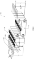
- an electrical converter 10 comprises a plurality of possibly identical converter modules 11 arranged between an AC interface with phase terminals referenced as a, b, c in case of three-phase operation ( Fig. 1 ) or g, N in case of single-phase operation ( Fig. 2 ), with g representing the line and N the neutral connection terminals.
- the electrical converter 10 is hence capable of operating both in three-phase AC to DC conversion and in single-phase AC to DC conversion.
- the electrical converter 10 as shown in Figs. 1 and 2 comprises six converter modules 11 which are all referenced to the negative DC link rail n which in turn is connected to the negative DC terminal DC - .
- two converter modules 11 are connected in parallel to each phase terminal a, b, c, hence forming three groups 101, 102, 103 of two parallel converter modules each.
- the neutral terminal N is advantageously not connected to any of the converter modules, nor to the negative DC terminal.
- the two converter modules of each group 101, 102, 103 advantageously equally share the respective phase current i a , i b , i c , i.e.
- i 1 i a /2.
- the electrical converter 10 is reconfigured such that three converter modules 11 are connected in parallel to each terminal g (grid line) and N (neutral), hence forming two groups 104, 105 of three parallel converter modules 11 each.
- the electrical converter comprises p 1 ⁇ k modules, advantageously p 1 x p 2 x k modules, with p 1 , p 2 and k being positive integers ( ⁇ N 1 ), advantageously p 1 > p 2 , and the electrical converter is reconfigurable between a first state of operation for converting between a first AC signal having p 1 phase voltages and a DC signal and between a second state of operation for converting between a second AC signal having p 2 phase voltages and the DC signal.
- the reconfiguration between these two states of operation is effected by arranging the converter modules in p 1 groups of p 2 k parallel operated converter modules in the first state of operation and in p 2 groups of p 1 k parallel operated converter modules in the second state of operation.
- the presence of p 1 x p 2 x k modules states a degree of freedom for the converter configuration, such that the converter modules are regrouped depending on whether p 1 - or p 2 -phase operation is performed, allowing in both cases utilization of all modules for power conversion.
- Reconfiguration can be effected manually or automatically, such as through mechanical contact switches or relays.
- the converter modules of all groups are parallel connected to the DC link capacitor C dc which has terminals connected to the positive DC terminal DC + and to the negative DC terminal DC - respectively.
- a suitable filter structure 14 can be provided at the AC side of the electrical converter in order to comply with electromagnetic interference (EMI) emission standards in both three-phase and single-phase operation.
- Filter structure 14 advantageously comprises a common mode (CM) filter.
- the common mode filter can comprise or consist of a common mode choke L CM advantageously having a number of windings equal to the number of converter modules, e.g. for the six-converter module electrical converter 10, L CM is a six-winding choke.
- a differential mode filter can be provided as known in the art.
- the filter structure 14 can comprise one or more of: common mode capacitors C CM , differential mode capacitors C DM , differential mode inductors L DM and common mode inductors L CM .
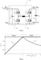
- Converter module 11 comprises two stages 12 and 13.
- the first stage 12 is connected across the AC-side capacitor C and comprises a switch node A.
- the AC-side capacitor C is connected between the AC node a 1 and the negative DC link rail n.
- the first stage 12 comprises a suitable conversion circuitry, such as a half-bridge with active switches T 1 and T 2 respectively connecting opposite terminals of capacitor C (i.e., the AC node a, and the negative DC-link rail n ) to the switch node A.
- the respective branch of filter structure 14 ( Fig. 1 ) of electrical converter 10 is omitted.
- any suitable filter branch may be connected between phase terminal a and the AC node a, of the converter module.
- the second stage 13 is connected between the positive DC link node p and the negative DC link rail n, and comprises a switch node B.
- the second stage 13 comprises a suitable conversion circuitry, such as a half-bridge with active switches T 3 and T 4 respectively connecting the positive DC link rail (node p ) and the negative DC link rail n to the switch node B.
- Switch nodes A and B are connected to opposite terminals of a physical inductor L .
- each converter module 11 to independently perform buck-boost AC/DC conversion between an AC signal at node a, and a DC signal between nodes p and n.
- the first stage 12 is operated when buck converter operation is required
- the second stage 13 is operated when boost converter operation is required.
- the buck and boost stages are advantageously operated in a mutually exclusive fashion, meaning that only one of the two stages 12, 13 are pulse width modulated at a point of time, while the other stage has its switch node A, B clamped to the respective AC node a 1 , and the positive DC link node p , respectively.
- the half bridges of the first stage 12 and/or the second stage 13 can be replaced with any other suitable conversion circuitry allowing to obtain single stage buck or boost AC/DC conversion.
- a suitable conversion circuitry is a (multi-level) flying capacitor circuit such as described in Dutch patent application No. 2026176 filed on 30 July 2020 , the contents of which are incorporated herein by reference.
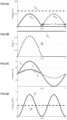
- Boost operation mode (of converter module 11 linked to AC terminal a) is selected when the respective phase input voltage u an is lower than U dc .
- the upper switch T 1 of the buck bridge-leg (stage 12) is permanently turned on and hence the switch node A of stage 12 is clamped to the AC terminal voltage.
- the boost stage 13 is controlled through pulse width modulation (PWM) such that the voltage of switch node B has a local average value (i.e. averaged over one pulse period) equal to the AC terminal voltage.
- PWM pulse width modulation
- a second order input filter is advantageously formed by the phase inductor L and the AC-side capacitor C .
- Buck operation mode is selected when u an exceeds U dc .
- the upper switch T 3 of the boost bridge-leg (stage 13) is permanently turned on and the switch node B of the boost stage 13 is clamped to the positive DC link rail (node p ).
- Stage 12 is now PWM operated in order to step down the AC terminal voltage, such that the voltage of switch node A has a local average value equal to the DC voltage U dc .
- the AC-side capacitor C is acting as an input filter and the inductor current i L1 shows an elevated fundamental (local average) current ⁇ i L1 ⁇ ⁇ i 1 .
- the active switches T 1 , T 2 of the buck stage 12 and T 3 , T 4 of the boost stage 13 are advantageously semiconductor switching devices, e.g. Field Effect Transistors (FETs), in particular MOSFET devices.
- FETs Field Effect Transistors
- the duty cycles are graphically represented in Fig. 4 . These duty cycles ensure the mutually exclusive high-frequency operation of buck and boost stages 12, 13 respectively. Also, as can be seen from Fig. 4 , both duty cycles d A and d B are advantageously continuous, allowing a simple control structure, avoiding transient oscillations during the changeover of the modulation regions.
- the electrical converter 10 is configured such that the six converter modules 11 are grouped in three groups 101-103 of each two converter modules operating in parallel and connected to a respective one of the three phase terminals a , b, c .
- the converter modules are operated independently as indicated above with half the phase current.
- a constant instantaneous power P equal to the desired average output power P , is drawn from the grid.
- DPWM Discontinuous Pulse Width Modulation
- the electrical converter 10 is configured such that the six converter modules 11 are grouped in two groups 104, 105 of three parallel converter modules.
- the converter modules of group 105 are connected to the line g and those of group 104 to the neutral terminal N of the grid.
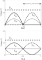
- the voltages between the AC terminals g, N and the negative DC link rail n i.e. the voltages across the capacitor C, denoted u gn and u Nn are strictly positive, allowing the converter modules to be operated as DC/DC converters.
- each group 104, 105 of converter modules is clamped, i.e. T 1 and T 4 are permanently on, during one half of the grid fundamental period T ac in which the respective phase has the lowest voltage, allowing for reducing the number of switching actions by 50%.
- the other group of 104, 105 having the highest phase voltage during the half of the grid fundamental period is operated normally as described above (i.e. boost or buck operation with PWM).
- a terminal voltage offset u off ( u gn + u Nn )/2 with respect to the negative DC link rail n cancels out and states a degree of freedom for the single-phase operation allowing to redistribute conduction and switching stresses among the power semiconductors of the converter modules.
- Fig. 7 shows a first possible terminal voltage waveform.
- the terminal voltage offset u off is time varying allowing each group 104 and 105 of converter modules to be PWM operated only during 50 % of the fundamental period T ac .
- Fig. 8 shows a second possible terminal voltage waveform with a constant terminal voltage offset. In the latter case, both groups 104 and 105 of converter modules need to be PWM operated continuously.
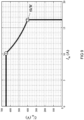
- FIG. 9 A current stress analysis was performed for the electrical converter as shown in Fig. 1 and Fig. 2 , both for three-phase and for single-phase operation. To this end, two operating points 1 and 2 were selected as indicated in Fig. 9 .
- Table 1 the line current
- i g or i a is elevated by a factor of three in single-phase operation (compared to three-phase operation), but as it is shared among 3k paralleled converter modules, the line current has no direct influence on the component stresses and hence on the component dimensioning.
- the converter module input current i 1 represents the predominant loss driver in the inductive components of the EMI filter (i.e. L CM , L DM / CM in Figs. 1 and 2 ) and is elevated by a factor of two in single-phase operation. Hence, a filter component overdimensioning would be advantageous.
- i a and i g correspond to the line current, in three-phase and single-phase operation, respectively and i T1 , i T2 , i T3 , i T4 are the currents through the semiconductor switches T 1 , T 2 , T 3 , T 4 , respectively.
- the line current is split equally among the parallel modules within a group, where the maximally occurring stresses of each component within the considered operating points are highlighted in bold and compared for three-phase (2 paralleled converter modules) and single-phase (three paralleled converter modules) operation, respectively.
- the current stresses of T 4 can be reduced by selecting a higher offset voltage u off and/or by advantageously turning on T 2 (with low current stresses in single-phase operation) during the clamping interval of T 1 and T 4 indicated in Fig. 6A , allowing current sharing between T 2 and T 4 and reduced overall conduction losses.
- the converter 10 comprises a control unit 15 configured to operate the electrical converter, both in three-phase operation and in single-phase operation.
- the control unit 15 can comprise individual control modules for operating the different converter modules 11 in a modular / independent fashion.
- the control unit 15 is advantageously configured to perform power factor correction (PFC) rectifier control with a cascaded control structure as known in the art.
- Measurement means are advantageously provided for measuring the three-phase AC grid voltages u a , u b , u c , single-phase AC grid voltage u gN and three-phase grid currents i a , i b , i c , single-phase grid current i g and the inductor current i L .
- measurement means are advantageously provided for measuring the DC terminal voltage U dc and advantageously the DC terminal current I dc . These measurements are advantageously input to control unit 15.
- single-phase current control is performed through single-phase current control block 152.
- the grid input power P is fluctuating with twice the mains frequency, and accordingly the measured DC voltage is advantageously processed with a notch filter (not shown) before comparing to its reference value.
- a grid current reference i g * elevated by a factor of 3 (compared to three-phase operation) and again in phase with the measured grid voltage u gN is set in order to provide the desired average output power.
- the input terminal voltage references u an * , u Nn * are derived.
- the offset voltage reference can be set to a constant value, or a time varying value, e.g. such that the lower terminal voltage reference is equal to zero.
- the control module 16 comprises an AC voltage control block 161, an inductor current control block 162, and a modulator 163.
- the output signal of the inductor current control block 162 is fed into the modulator 163, generating duty cycles for the mutually exclusive operation of buck stage 12 and boost stage 13.
- the control signals for the active switches T 1 , T 2 , T 3 and T 4 are then generated using PWM from the generated duty cycles as known in the art.
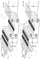
- the electrical converter 10 can be provided with additional switching means 112 (e.g. mechanical contact switches or relays) to interconnect the AC-sided terminals 111 of the AC-side capacitors C of all converter modules within one group.
- the interconnection allows the interleaved currents to at least partially cancel out when interleaved PWM operation between the converter modules of one group is performed, advantageously reducing the required filter attenuation to comply with EMI regulations.
- the interconnections between terminals 111 can be provided either for three-phase operation ( Fig. 11A ), for single-phase operation ( Fig. 11B ), or both for three-phase and single-phase operation.
- the interconnections 112 are advantageously switchable allowing for possibly automatic reconfiguration when reconfiguring between three-phase and single-phase operation modes.
- the semiconductors T 1 are permanently turned on and T 3 and T 2 /T 4 are alternatingly clamped to p and n , respectively at half the grid fundamental period.
- the converter modules of group 104 therefore would have elevated semiconductor conduction stresses, but practically no switching losses. Therefore fewer converter modules can be used for this purpose, e.g. two converter modules would be sufficient for this task, and the remaining (third) converter module can be additionally assigned to group 105 connected to the line terminal g .
- the converter modules of group 105 will be PWM operated as described above and therefore the semiconductor switches T 1 -T 4 are high-frequency (HF) operated hence facing both conduction and switching losses.
- the four converter modules of group 105 equally share 1 ⁇ 4 of the grid current compared to 1/3 of the grid current for the configuration of Fig. 2 . Thereby the current stresses on the semiconductors can be reduced while semiconductor utilization can be improved.
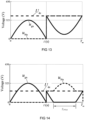
- the terminal voltage waveforms for the converter configuration according to Fig. 12A in single-phase operation are shown in Fig. 13 for boost operation and Fig. 14 for buck and boost operation.
- Fig. 13 when the DC link voltage U dc is higher than u gn , the group 104 converter modules are permanently in unfolder operation. In this case, u Nn is block shaped on a fundamental frequency level, while u gN needs to be sinusoidal.
- the terminal voltage waveforms in buck operation are shown in Fig. 14 .
- the group 104 converter modules i.e. assigned to terminal N, are operated as unfolder circuits except for a short period T PWM when u Nn exceeds U dc .
- the group 104 converter modules are PWM operated, e.g. based on the control strategy described above in relation to Fig. 10 .
- the group 105 converter modules are advantageously clamped, i.e. T 1 and T 4 are permanently on.
- the converter module configuration of Fig. 12A for single-phase operation i.e. two converter modules arranged in group 104 connected to N and four converter modules arranged in group 105 connected to g is kept, while the AC side filter structure 14 is equally shared between the two AC terminals g and N, i.e. in a 3-3 configuration.
- the AC filter 14 is connected to the AC terminals such that the windings of the differential mode and/or common mode inductors L DM / CM and L CM are equally shared between the terminals g and N, just like the configuration of Fig.
- filter group 141 is connected between terminal N and the group 104 converter modules
- filter group 142 is connected between terminal g and the group 105 converter modules.
- the additional switching means 112 which interconnect the AC-sided terminals 111 of the AC-side capacitors C of converter modules within one group, as shown in Fig. 12B .
- at least one of the switching means 112 should allow to disconnect a converter module from its respective AC filter branch, as shown in Fig. 12B . This allows to evenly distribute the fundamental frequency current stresses within the AC filter 14 while retaining the advantage of the 4/2 configuration of the converter modules.
- a time-varying power P pulsating at twice the line frequency is drawn from the grid as shown in Fig. 6D .
- the output power ripple can be reduced by providing a DC link capacitor C dc of appropriate size.
- an active power pulsation buffer PPB
- the active PPB can comprise a buffer capacitor and a converter circuit, such as a half-bridge converter, interfacing between the DC link and the buffer capacitor.
- the converter circuit can be provided as being identical to the converter module 11.
- the buck-boost capability of the converter module used as PPB advantageously allows to vary the buffer capacitor voltage in a wide range both above and below the desired DC link voltage.
- one or more of the converter modules 21 of the electrical converter 20, e.g. converter module 22, can be provided with a respective buffer capacitor C PPB for use as PPB in single-phase operation.
- Converter modules 21, 22 can be identical to the converter modules 11 described hereinabove.
- C PPB is disconnected from the AC terminal a allowing converter module 22 to operate along with the other converter modules 21 in modular groups connected to the respective AC terminals a , b, c as described in relation to Fig. 1 .
- single-phase operation as shown in Fig.
- the converter module 22 is disconnected from the AC grid and the buffer capacitor C PPB is parallel connected to the filter capacitors C and/or C DM/CM to operate as a PPB.
- the voltage across C PPB can be both above and below the DC link voltage U dc .
- the common mode choke L CM is disconnected at node 211 from the buffer capacitors / converter module 22, this is not a requirement and the common mode choke can be left attached.
- the buffer capacitor C PPB is optional, e.g. when the capacitors C and/or C DM/CM provide sufficient energy storage capability.
- the PPB converter modules reduce the minimum DC link capacitance value for single-phase operation.
- the converter module 22 acting as PPB is modified by providing a suitable switching circuitry 212 allowing in single-phase operation to disconnect switch node B from switch node A while operably connecting the buffer capacitor C PPB to switch node B.
- the switching circuitry 212 is configured to disconnect switch node A from the respective terminal 213 of inductor L while connecting terminal 213 to C PPB .
- the switching circuitry 212 is advantageously further configured to connect the bridge-leg T 1 /T 2 across the positive and negative DC link rails p and n, while the switch node A is connected to the neutral terminal N.
- converter module 22 is split such that only the boost stage 13 acts as a PPB 23 (now with a PPB voltage strictly below the DC link voltage).
- the bridge-leg T 1 /T 2 acts as an unfolder circuit 24, allowing to parallel the converter modules 21 parallel connected to terminal g, and which are hence equally sharing the grid current.
- the converter modules 21 and possibly 22 referenced in Figs. 15A-B and 16A-B can refer to single converter modules as the converter modules 11 described previously, or alternatively can refer to groups 101-103 and 104-105 of converter modules as described in any of the above embodiments.
- the 4/2 converter module configuration as described in relation to Figs. 12A and 12B can be adapted such that one of the four group 105 converter modules 11 is used as a PPB.
- a configuration with three group 105 converter modules, two group 104 converter modules and one PPB module is obtained in single-phase operation, while all six converter modules 11 would be available for being assigned to groups 101-103 in three-phase operation.
- the electrical converter as described herein can be operated as inverter, both for three-phase and single-phase operation, with a similar control structure as described above. Furthermore, bidirectional power flow through the electrical converter is possible, allowing it to be used for power injection into the AC grid.
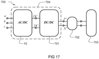
- a battery charging system 700 comprises a power supply unit 704.
- the power supply unit 704 is coupled on one side to the AC grid through terminals a, b, c and on the other side (at terminals P', N') to an interface 702, e.g. comprising a switch device, which allows to connect the power supply unit 704 to a battery 703.
- the power supply unit 704 comprises any one of the electrical converters, e.g. converter 10, as described hereinabove and can comprise a further converter stage 701, which in the present system is a DC-DC converter.
- the converter stage 701 can comprise a pair of coils which are inductively coupled through air (not shown), such as in the case of wireless power transfer.
- the DC-DC converter stage 701 can comprise or consist of one or more possibly isolated DC-DC converters.
- the interface 702 can comprise a plug and socket, e.g. in wired power transfer.
- the plug and socket can be provided at the input (e.g., at nodes a, b, c).
- Another possible application of electrical converters according to the present disclosure is as a traction inverter of an electric motor drive system.
Landscapes
- Engineering & Computer Science (AREA)
- Power Engineering (AREA)
- Transportation (AREA)
- Mechanical Engineering (AREA)
- Rectifiers (AREA)
- Inverter Devices (AREA)
- Dc-Dc Converters (AREA)
Claims (15)
- Elektrischer Wandler (10, 20) zum Umwandeln zwischen einem Wechselstromsignal und einem Gleichstromsignal, umfassend:eine Vielzahl von Wechselstromanschlüssen (a, b, c, g, N), einen ersten und einen zweiten Gleichstromanschluss (DC+, DC-),eine Vielzahl von Wandlermodulen (11, 21, 22), wobei jedes der Vielzahl von Wandlermodulen Folgendes umfasst:einen Wechselstromknoten (a1, 111),einen ersten Kondensator (C), wobei der Wechselstrom knoten (a1, 111) mit einem ersten Anschluss des ersten Kondensators verbunden ist und der zweite Gleichstromanschluss (DC-) mit einem dem ersten Anschluss gegenüberliegenden zweiten Anschluss des ersten Kondensators verbunden ist, sodass der zweite Gleichstromanschluss einen gemeinsamen Knoten mit den ersten Kondensatoren (C) der Vielzahl von Wandlermodulen bildet,eine erste Wandlerstufe (12), die einen ersten Schaltknoten (A) und eine Halbbrücke mit einem ersten aktiven Halbleiterschalter (T1), der den ersten Anschluss des ersten Kondensators mit dem ersten Schaltknoten (A) verbindet, und einem zweiten aktiven Halbleiterschalter (T2), der den zweiten Anschluss des ersten Kondensators mit dem ersten Schaltknoten (A) verbindet, umfasst,eine zweite Wandlerstufe (13), die einen zweiten Schaltknoten (B) und eine Halbbrücke mit einem dritten aktiven Halbleiterschalter (T3), der den ersten Gleichstromanschluss mit dem zweiten Schaltknoten (B) verbindet, und einem vierten aktiven Halbleiterschalter (T4), der den zweiten Gleichstromanschluss mit dem zweiten Schaltknoten (B) verbindet, umfasst,einen ersten Induktor (L), wobei der erste und der zweite Schaltknoten mit gegenüberliegenden Anschlüssen des ersten Induktors verbunden sind,wobei eine Verbindung zwischen den Wechselstromknoten (a1, 111) der Vielzahl von Wandlermodulen und der Vielzahl von Wechselstromanschlüssen rekonfigurierbar ist, was es dem elektrischen Wandler ermöglicht, gemäß einem ersten Betriebsmodus, der dazu konfiguriert ist, zwischen einem ersten Wechselstromsignal mit einer ersten Vielzahl p1 ≥ 3 von Phasenspannungen und dem Gleichstromsignal zu wandeln und gemäß einem zweiten Betriebsmodus, der dazu konfiguriert ist, zwischen einem zweiten Wechselstromsignal mit einphasiger Spannung und dem Gleichstromsignal zu wandeln, betrieben zu werden, sodass die Vielzahl von Wandlermodulen (11, 21, 22), die zum Wandeln zwischen dem ersten Wechselstromsignal und dem Gleichstromsignal in dem ersten Betriebsmodus beitragen, zu der Wandlung zwischen dem zweiten Wechselstromsignal und dem Gleichstromsignal oder zu einer aktiven kapazitiven Energiespeicherung (CPPB) für einen Leistungspulsationspuffer in dem zweiten Betriebsmodus beitragen,wobei die Vielzahl von Wandlermodulen mindestens p1 k Wandlermodule sind, wobei k eine positive ganze Zahl gleich oder größer zwei ist, wobei in dem ersten Betriebsmodus die p1 k Wandlermodule in p1 erste Gruppen (101, 102, 103) gruppiert sind und wobei in dem zweiten Betriebsmodus die p1 k Wandlermodule in zwei zweiten Gruppen (104, 105) neu angeordnet sind, wobei eine größere Anzahl der Vielzahl von Wandlermodulen einer ersten (105) der zwei zweiten Gruppen zugeordnet ist, und wobei mindestens zwei der Vielzahl von Wandlermodulen einer zweiten (104) der zwei zweiten Gruppen zugeordnet sind, wobei der elektrische Wandler dazu konfiguriert ist, mehrere Wandlermodule, die einer gleichen Gruppe der ersten Gruppen und der zweiten Gruppen zugeordnet sind, parallel zu betreiben,wobei der zweite Betriebsmodus einen Aufwärts-Betriebsmodus umfasst, in dem der elektrische Wandler dazu konfiguriert ist, die Vielzahl von Wandlermodulen, die der ersten (105) der zwei zweiten Gruppen zugeordnet sind, über Pulsweitenmodulation zu betreiben, und die Vielzahl von Wandlermodulen, die der zweiten (104) der zwei zweiten Gruppen zugeordnet sind, entsprechend einem Unfolder-Betrieb zu betreiben, wobei in dem "Unfolder"-Betrieb der erste aktive Halbleiterschalter (T1) geschaltet ist, um den ersten Schaltknoten (A) an den jeweiligen Wechselstrom knoten zu klemmen und der dritte aktive Halbleiterschalter (T3) und der zweite oder der vierte aktive Halbleiterschalter (T2, T4) geschaltet sind, um den zweiten Schaltknoten (B) abwechselnd an jeweils den ersten und den zweiten Gleichstromanschluss mit einer halben Grundperiode des zweiten Wechselstromsignals zu klemmen.
- Elektrischer Wandler nach Anspruch 1, wobei der zweite Betriebsmodus einen Abwärts-Betriebsmodus umfasst, in dem der elektrische Wandler dazu konfiguriert ist, die Vielzahl von Wandlermodulen, die der zweiten (104) der zwei zweiten Gruppen zugeordnet sind, entsprechend dem Unfolder-Betrieb zu betreiben, wenn eine Spannung an den jeweiligen ersten Kondensatoren (C) kleiner als oder gleich einer Spannung an dem ersten und dem zweiten Gleichstromanschluss (Udc) ist, und die Vielzahl von Wandlermodulen, die der zweiten (104) der zwei zweiten Gruppen zugeordnet sind, über Pulsweitenmodulation zu betreiben, wenn die Spannung an den jeweiligen ersten Kondensatoren (C) die Spannung an dem ersten und dem zweiten Gleichstromanschluss (Udc) überschreitet.
- Elektrischer Wandler nach Anspruch 2, wobei der elektrische Wandler in dem Abwärts-Betriebsmodus dazu konfiguriert ist, die Vielzahl von Wandlermodulen, die dem ersten (105) der zwei zweiten Gruppen zugeordnet sind, in einem geklemmten Modus betrieben werden, sodass der erste aktive Halbleiterschalter (T1) dazu geschaltet ist, den ersten Schaltknoten (A) an den jeweiligen Wechselstrom knoten zu klemmen und der vierte aktive Halbleiterschalter (T4) dazu geschaltet ist, den zweiten Schaltknoten (B) an den zweiten Gleichstromanschluss zu klemmen.
- Elektrischer Wandler nach einem der vorhergehenden Ansprüche, wobei die ersten Gruppen (101, 102, 103) eine gleiche Anzahl von Wandlermodulen (11, 21) aufweisen.
- Elektrischer Wandler nach einem der vorhergehenden Ansprüche, umfassend einen zweiten Kondensator (C dc ), der über den ersten und den zweiten Gleichstromanschluss verbunden ist, wobei die zweiten Wandlerstufen der Vielzahl von Wandlermodulen mit dem zweiten Kondensator parallel verbunden sind.
- Elektrischer Wandler nach einem der vorhergehenden Ansprüche, umfassend einen Wechselstromfilter (14), der zwischen der Vielzahl von Wechselstromanschlüssen (a, b, c, g, N) und den Wechselstromknoten (111) verbunden ist, wobei der Wechselstromfilter einen Gleichtaktfilter umfasst, der eine Gleichtaktdrossel, (LCM ) umfasst, wobei die Gleichtaktdrossel (LCM ) bevorzugt einer Zweig für jedes der Vielzahl von Wandlermodulen umfasst, wobei der Zweig mit dem Wechselstromknoten (111) des jeweiligen der Vielzahl von Wandlermodulen verbunden oder verbindbar ist.
- Elektrischer Wandler nach einem der vorhergehenden Ansprüche, umfassend ein erstes Schaltmittel (112) zum Miteinanderverbinden von Anschlüssen der ersten Kondensatoren (C) an einer Seite des Wechselstromknotens (111) auf eine rekonfigurierbare Weise, wobei bevorzugt das erste Schaltmittel (112) dazu konfiguriert ist, die Anschlüsse der ersten Kondensatoren (C) der Wandlermodule, die einer gleichen Gruppe der ersten Gruppen und/oder der zweiten Gruppen zugeordnet sind, miteinander zu verbinden, wobei die Gleichtaktdrossel (LCM ) bevorzugt einen Zweig für jedes der Vielzahl von Wandlermodulen umfasst, wobei der Zweig mit dem Wechselstromknoten (111) des jeweiligen der Vielzahl von Wandlermodulen verbunden oder verbindbar ist und wobei das Schaltmittel (112) dazu konfiguriert ist, eine erste Anzahl der Zweige mit einer zweiten Anzahl der Vielzahl von Wandlermodulen zu verbinden, wobei die erste Anzahl und die zweite Anzahl ungleich sind.
- Elektrischer Wandler nach einem der vorhergehenden Ansprüche, umfassend eine Steuerungseinheit (15), wobei die Steuerungseinheit dazu konfiguriert ist, jedes der Vielzahl von Wandlermodulen (11) entsprechend einem dritten Betriebsmodus zu betreiben, wobei eine Gleichstromspannung (Udc) an dem ersten und dem zweiten Gleichstromanschluss kleiner als oder gleich einer ersten Spannung (uan, ugn) an dem jeweiligen ersten Kondensator (C) ist, und nach einem vierten Betriebsmodus zu betreiben, wobei die Gleichstromspannung (Udc) größer ist als die erste Spannung (uan, ugn).
- Elektrischer Wandler nach einem der vorhergehenden Ansprüche, umfassend eine Steuerungseinheit (15), wobei die Steuerungseinheit dazu konfiguriert ist, den ersten und den zweiten aktiven Halbleiterschalter sich gegenseitig ausschließend über Pulsweitenmodulation und den dritten und den vierten aktiven Halbleiterschalter sich gegenseitig ausschließend über Pulsweitenmodulation zu betreiben, wobei die Steuerungseinheit bevorzugt dazu konfiguriert ist, das eine oder die mehreren ersten Wandlermodule über Pulsweitenmodulation in dem ersten Betriebsmodus zu betreiben.
- Elektrischer Wandler nach einem der vorhergehenden Ansprüche, umfassend eine Steuerungseinheit (15), wobei die Steuerungseinheit dazu konfiguriert ist, einen Arbeitszyklus (dA , dB ) für jedes der Vielzahl von Wandlermodulen unabhängig auf Basis einer ersten Referenzspannung (u*an, u*gn) an dem jeweiligen ersten Kondensator (C) zu bestimmen.
- Elektrischer Wandler nach einem der vorhergehenden Ansprüche, wobei mindestens eines der Vielzahl von Wandlermodulen (22) dazu konfiguriert ist, als ein Leistungspulsationspuffer in dem zweiten Betriebsmodus betrieben zu werden, wobei bevorzugt das mindestens eine Wandlermodul (21), das dazu konfiguriert ist, als ein Leistungspulsationspuffer betrieben zu werden, dazu konfiguriert ist, den ersten Kondensator (C) in dem zweiten Betriebsmodus zu laden und zu entladen.
- Elektrischer Wandler nach Anspruch 11, wobei das mindestens eine Wandlermodul (21), das dazu konfiguriert ist, als ein Leistungspulsationspuffer betrieben zu werden ferner einen Pufferkondensator (CPPB) und zweite Schaltmittel umfasst, und das zweite Schaltmittel dazu konfiguriert ist, den Pufferkondensator (CPPB) mit dem mindestens einem Wandlermodul (21) in dem zweiten Betriebsmodus zum Laden und Entladen des Pufferkondensators zu verbinden.
- Elektrischer Wandler nach Anspruch 12, wobei das zweite Schaltmittel dazu konfiguriert ist, den Pufferkondensator (CPPB) parallel mit dem ersten Kondensator (C) zu verbinden.
- Elektrischer Wandler nach Anspruch 12, wobei das zweite Schaltmittel (212) dazu konfiguriert ist, eine Verbindung eines Anschlusses (213) des ersten Induktors (L) zwischen dem ersten Schaltknoten (A) und einem Anschluss des Pufferkondensators (CPPB) so zu schalten, dass die zweite Wandlerstufe (13) betriebsfähig zum Laden und Entladen des Pufferkondensators in dem zweiten Betriebsmodus ist, wobei das zweite Schaltmittel (212) bevorzugt ferner dazu konfiguriert ist, ein Brückenbein (24) der ersten Wandlerstufe (12) zwischen dem ersten und dem zweiten Gleichstromanschluss und dem ersten Schaltknoten (A) mit einem jeweilige Wechselstromanschluss in dem zweiten Betriebsmodus zu verbinden.
- Batterieladesystem, insbesondere zum Laden von Antriebsbatterien für elektrische Fahrzeuge, wobei das Batterieladesystem eine Stromversorgung umfasst, wobei die Stromversorgung den elektrischen Wandler (10) nach einem der vorhergehenden Ansprüche umfasst.
Applications Claiming Priority (2)
| Application Number | Priority Date | Filing Date | Title |
|---|---|---|---|
| NL2026324A NL2026324B1 (en) | 2020-08-21 | 2020-08-21 | Modular reconfigurable electrical AC/DC converter |
| PCT/EP2021/073198 WO2022038288A1 (en) | 2020-08-21 | 2021-08-20 | Modular reconfigurable electrical ac/dc converter |
Publications (3)
| Publication Number | Publication Date |
|---|---|
| EP4200964A1 EP4200964A1 (de) | 2023-06-28 |
| EP4200964B1 true EP4200964B1 (de) | 2024-09-04 |
| EP4200964C0 EP4200964C0 (de) | 2024-09-04 |
Family
ID=72802119
Family Applications (1)
| Application Number | Title | Priority Date | Filing Date |
|---|---|---|---|
| EP21763104.3A Active EP4200964B1 (de) | 2020-08-21 | 2021-08-20 | Modularer rekonfigurierbarer elektrischer wechselstrom-gleichstrom-wandler |
Country Status (8)
| Country | Link |
|---|---|
| US (1) | US20230336072A1 (de) |
| EP (1) | EP4200964B1 (de) |
| JP (1) | JP2023542475A (de) |
| KR (1) | KR20230052286A (de) |
| CN (1) | CN116686205A (de) |
| IL (1) | IL300793A (de) |
| NL (1) | NL2026324B1 (de) |
| WO (1) | WO2022038288A1 (de) |
Families Citing this family (4)
| Publication number | Priority date | Publication date | Assignee | Title |
|---|---|---|---|---|
| NL2026176B1 (en) * | 2020-07-30 | 2022-04-04 | Prodrive Tech Innovation Services B V | Multi-level bidirectional electrical AC/DC converter |
| US12062983B2 (en) * | 2021-11-08 | 2024-08-13 | Pacific Energy Inc. | Modular high power bi-directional half bridge buck/boost converter assembly |
| EP4280447A1 (de) * | 2022-05-18 | 2023-11-22 | KONE Corporation | Regenerativer frequenzumrichter und aufzugssystem |
| CN220368612U (zh) * | 2023-05-25 | 2024-01-19 | 内江市凌辉电子科技有限公司 | 一种三相交流四开关Buck-Boost双向变换器 |
Family Cites Families (7)
| Publication number | Priority date | Publication date | Assignee | Title |
|---|---|---|---|---|
| DE2026176A1 (de) | 1970-05-29 | 1971-12-09 | Stute G | Vorrichtung zur Verbindung eines Pro zessrechners mit numerisch gesteuerten Fer tigungsvornchtungen |
| GB0625121D0 (en) * | 2006-12-18 | 2007-01-24 | Gendrive Ltd | Electrical energy converter |
| WO2010086788A2 (en) * | 2009-01-29 | 2010-08-05 | Brusa Elektronik Ag | Converter for single-phase and three-phase operation, d.c. voltage supply and battery charger |
| DE102014211853A1 (de) * | 2014-06-20 | 2015-12-24 | Robert Bosch Gmbh | Spannungskonverter und Verfahren zum Konvertieren einer elektrischen Spannung |
| CH714180B1 (de) * | 2017-09-20 | 2021-11-15 | Eth Zuerich | Konverter zur Übertragung von elektrischer Energie zwischen einem DC und einem AC-System. |
| DE102018116486A1 (de) * | 2018-07-06 | 2020-01-09 | HELLA GmbH & Co. KGaA | Kopplungsvorrichtung |
| CH715448A2 (de) | 2018-10-15 | 2020-04-15 | Prodrive Tech Bv | Mehrphasige Umrichtertopologie für mehrphasigen und einphasigen Betrieb. |
-
2020
- 2020-08-21 NL NL2026324A patent/NL2026324B1/en active
-
2021
- 2021-08-20 CN CN202180066179.9A patent/CN116686205A/zh active Pending
- 2021-08-20 EP EP21763104.3A patent/EP4200964B1/de active Active
- 2021-08-20 IL IL300793A patent/IL300793A/en unknown
- 2021-08-20 JP JP2023512407A patent/JP2023542475A/ja active Pending
- 2021-08-20 WO PCT/EP2021/073198 patent/WO2022038288A1/en not_active Ceased
- 2021-08-20 KR KR1020237009042A patent/KR20230052286A/ko not_active Withdrawn
- 2021-08-20 US US18/042,339 patent/US20230336072A1/en active Pending
Also Published As
| Publication number | Publication date |
|---|---|
| EP4200964C0 (de) | 2024-09-04 |
| US20230336072A1 (en) | 2023-10-19 |
| EP4200964A1 (de) | 2023-06-28 |
| WO2022038288A1 (en) | 2022-02-24 |
| JP2023542475A (ja) | 2023-10-10 |
| KR20230052286A (ko) | 2023-04-19 |
| NL2026324B1 (en) | 2022-04-14 |
| CN116686205A (zh) | 2023-09-01 |
| IL300793A (en) | 2023-04-01 |
Similar Documents
| Publication | Publication Date | Title |
|---|---|---|
| EP4200964B1 (de) | Modularer rekonfigurierbarer elektrischer wechselstrom-gleichstrom-wandler | |
| CA2489345C (en) | Impedance source power converter | |
| EP3837759B1 (de) | Stromwandler | |
| CN114069807B (zh) | 具有集成整流器的增强型单级车载充电器的系统和方法 | |
| KR102726658B1 (ko) | 전력 변환기 | |
| US20220190744A1 (en) | Electrical converter | |
| CN108242813B (zh) | 电能质量综合治理和功率优化的能量路由器的控制方法 | |
| US20230155518A1 (en) | Electrical power converter | |
| EP4147341B1 (de) | Elektrischer leistungswandler | |
| EP4147340B1 (de) | Elektrischer leistungswandler | |
| US20220278607A1 (en) | Electrical converter | |
| Mohseni et al. | Novel Concept of Universal AC/DC-DC Onboard Battery Charger for Electric Vehicles | |
| CN120546465A (zh) | 一种四开关交直流双输出无直通风险的升降压变换器及控制方法 | |
| CN121710655A (zh) | 功率转换器以及用于控制该功率转换器的方法 |
Legal Events
| Date | Code | Title | Description |
|---|---|---|---|
| STAA | Information on the status of an ep patent application or granted ep patent |
Free format text: STATUS: UNKNOWN |
|
| STAA | Information on the status of an ep patent application or granted ep patent |
Free format text: STATUS: THE INTERNATIONAL PUBLICATION HAS BEEN MADE |
|
| PUAI | Public reference made under article 153(3) epc to a published international application that has entered the european phase |
Free format text: ORIGINAL CODE: 0009012 |
|
| STAA | Information on the status of an ep patent application or granted ep patent |
Free format text: STATUS: REQUEST FOR EXAMINATION WAS MADE |
|
| 17P | Request for examination filed |
Effective date: 20230308 |
|
| AK | Designated contracting states |
Kind code of ref document: A1 Designated state(s): AL AT BE BG CH CY CZ DE DK EE ES FI FR GB GR HR HU IE IS IT LI LT LU LV MC MK MT NL NO PL PT RO RS SE SI SK SM TR |
|
| DAV | Request for validation of the european patent (deleted) | ||
| DAX | Request for extension of the european patent (deleted) | ||
| REG | Reference to a national code |
Free format text: PREVIOUS MAIN CLASS: H02M0001100000 Ipc: H02M0001000000 Ref country code: DE Ref legal event code: R079 Ref document number: 602021018404 Country of ref document: DE |
|
| GRAP | Despatch of communication of intention to grant a patent |
Free format text: ORIGINAL CODE: EPIDOSNIGR1 |
|
| STAA | Information on the status of an ep patent application or granted ep patent |
Free format text: STATUS: GRANT OF PATENT IS INTENDED |
|
| RIC1 | Information provided on ipc code assigned before grant |
Ipc: H02M 7/81 20060101ALI20240319BHEP Ipc: H02M 1/10 20060101ALI20240319BHEP Ipc: H02J 7/02 20160101ALI20240319BHEP Ipc: B60L 53/22 20190101ALI20240319BHEP Ipc: H02M 1/00 20060101AFI20240319BHEP |
|
| INTG | Intention to grant announced |
Effective date: 20240405 |
|
| GRAS | Grant fee paid |
Free format text: ORIGINAL CODE: EPIDOSNIGR3 |
|
| GRAA | (expected) grant |
Free format text: ORIGINAL CODE: 0009210 |
|
| STAA | Information on the status of an ep patent application or granted ep patent |
Free format text: STATUS: THE PATENT HAS BEEN GRANTED |
|
| AK | Designated contracting states |
Kind code of ref document: B1 Designated state(s): AL AT BE BG CH CY CZ DE DK EE ES FI FR GB GR HR HU IE IS IT LI LT LU LV MC MK MT NL NO PL PT RO RS SE SI SK SM TR |
|
| REG | Reference to a national code |
Ref country code: GB Ref legal event code: FG4D |
|
| REG | Reference to a national code |
Ref country code: CH Ref legal event code: EP |
|
| REG | Reference to a national code |
Ref country code: IE Ref legal event code: FG4D |
|
| REG | Reference to a national code |
Ref country code: DE Ref legal event code: R096 Ref document number: 602021018404 Country of ref document: DE |
|
| U01 | Request for unitary effect filed |
Effective date: 20240917 |
|
| U07 | Unitary effect registered |
Designated state(s): AT BE BG DE DK EE FI FR IT LT LU LV MT NL PT RO SE SI Effective date: 20241008 |
|
| PG25 | Lapsed in a contracting state [announced via postgrant information from national office to epo] |
Ref country code: NO Free format text: LAPSE BECAUSE OF FAILURE TO SUBMIT A TRANSLATION OF THE DESCRIPTION OR TO PAY THE FEE WITHIN THE PRESCRIBED TIME-LIMIT Effective date: 20241204 |
|
| PG25 | Lapsed in a contracting state [announced via postgrant information from national office to epo] |
Ref country code: PL Free format text: LAPSE BECAUSE OF FAILURE TO SUBMIT A TRANSLATION OF THE DESCRIPTION OR TO PAY THE FEE WITHIN THE PRESCRIBED TIME-LIMIT Effective date: 20240904 Ref country code: GR Free format text: LAPSE BECAUSE OF FAILURE TO SUBMIT A TRANSLATION OF THE DESCRIPTION OR TO PAY THE FEE WITHIN THE PRESCRIBED TIME-LIMIT Effective date: 20241205 |
|
| PG25 | Lapsed in a contracting state [announced via postgrant information from national office to epo] |
Ref country code: HR Free format text: LAPSE BECAUSE OF FAILURE TO SUBMIT A TRANSLATION OF THE DESCRIPTION OR TO PAY THE FEE WITHIN THE PRESCRIBED TIME-LIMIT Effective date: 20240904 |
|
| PG25 | Lapsed in a contracting state [announced via postgrant information from national office to epo] |
Ref country code: ES Free format text: LAPSE BECAUSE OF FAILURE TO SUBMIT A TRANSLATION OF THE DESCRIPTION OR TO PAY THE FEE WITHIN THE PRESCRIBED TIME-LIMIT Effective date: 20240904 Ref country code: RS Free format text: LAPSE BECAUSE OF FAILURE TO SUBMIT A TRANSLATION OF THE DESCRIPTION OR TO PAY THE FEE WITHIN THE PRESCRIBED TIME-LIMIT Effective date: 20241204 |
|
| PG25 | Lapsed in a contracting state [announced via postgrant information from national office to epo] |
Ref country code: RS Free format text: LAPSE BECAUSE OF FAILURE TO SUBMIT A TRANSLATION OF THE DESCRIPTION OR TO PAY THE FEE WITHIN THE PRESCRIBED TIME-LIMIT Effective date: 20241204 Ref country code: PL Free format text: LAPSE BECAUSE OF FAILURE TO SUBMIT A TRANSLATION OF THE DESCRIPTION OR TO PAY THE FEE WITHIN THE PRESCRIBED TIME-LIMIT Effective date: 20240904 Ref country code: NO Free format text: LAPSE BECAUSE OF FAILURE TO SUBMIT A TRANSLATION OF THE DESCRIPTION OR TO PAY THE FEE WITHIN THE PRESCRIBED TIME-LIMIT Effective date: 20241204 Ref country code: HR Free format text: LAPSE BECAUSE OF FAILURE TO SUBMIT A TRANSLATION OF THE DESCRIPTION OR TO PAY THE FEE WITHIN THE PRESCRIBED TIME-LIMIT Effective date: 20240904 Ref country code: GR Free format text: LAPSE BECAUSE OF FAILURE TO SUBMIT A TRANSLATION OF THE DESCRIPTION OR TO PAY THE FEE WITHIN THE PRESCRIBED TIME-LIMIT Effective date: 20241205 Ref country code: ES Free format text: LAPSE BECAUSE OF FAILURE TO SUBMIT A TRANSLATION OF THE DESCRIPTION OR TO PAY THE FEE WITHIN THE PRESCRIBED TIME-LIMIT Effective date: 20240904 |
|
| PG25 | Lapsed in a contracting state [announced via postgrant information from national office to epo] |
Ref country code: IS Free format text: LAPSE BECAUSE OF FAILURE TO SUBMIT A TRANSLATION OF THE DESCRIPTION OR TO PAY THE FEE WITHIN THE PRESCRIBED TIME-LIMIT Effective date: 20250104 |
|
| PG25 | Lapsed in a contracting state [announced via postgrant information from national office to epo] |
Ref country code: SM Free format text: LAPSE BECAUSE OF FAILURE TO SUBMIT A TRANSLATION OF THE DESCRIPTION OR TO PAY THE FEE WITHIN THE PRESCRIBED TIME-LIMIT Effective date: 20240904 |
|
| PG25 | Lapsed in a contracting state [announced via postgrant information from national office to epo] |
Ref country code: CZ Free format text: LAPSE BECAUSE OF FAILURE TO SUBMIT A TRANSLATION OF THE DESCRIPTION OR TO PAY THE FEE WITHIN THE PRESCRIBED TIME-LIMIT Effective date: 20240904 |
|
| PG25 | Lapsed in a contracting state [announced via postgrant information from national office to epo] |
Ref country code: SK Free format text: LAPSE BECAUSE OF FAILURE TO SUBMIT A TRANSLATION OF THE DESCRIPTION OR TO PAY THE FEE WITHIN THE PRESCRIBED TIME-LIMIT Effective date: 20240904 |
|
| PLBE | No opposition filed within time limit |
Free format text: ORIGINAL CODE: 0009261 |
|
| STAA | Information on the status of an ep patent application or granted ep patent |
Free format text: STATUS: NO OPPOSITION FILED WITHIN TIME LIMIT |
|
| 26N | No opposition filed |
Effective date: 20250605 |
|
| U20 | Renewal fee for the european patent with unitary effect paid |
Year of fee payment: 5 Effective date: 20250827 |
|
| U1N | Appointed representative for the unitary patent procedure changed after the registration of the unitary effect |
Representative=s name: ARNOLD & SIEDSMA; NL |
|
| REG | Reference to a national code |
Ref country code: CH Ref legal event code: H13 Free format text: ST27 STATUS EVENT CODE: U-0-0-H10-H13 (AS PROVIDED BY THE NATIONAL OFFICE) Effective date: 20260324 |
|
| PG25 | Lapsed in a contracting state [announced via postgrant information from national office to epo] |
Ref country code: MC Free format text: LAPSE BECAUSE OF FAILURE TO SUBMIT A TRANSLATION OF THE DESCRIPTION OR TO PAY THE FEE WITHIN THE PRESCRIBED TIME-LIMIT Effective date: 20240904 |