EP4199331A1 - Hybrider schaltwandler, verfahren zu dessen betrieb und beleuchtungssystem - Google Patents
Hybrider schaltwandler, verfahren zu dessen betrieb und beleuchtungssystem Download PDFInfo
- Publication number
- EP4199331A1 EP4199331A1 EP21214714.4A EP21214714A EP4199331A1 EP 4199331 A1 EP4199331 A1 EP 4199331A1 EP 21214714 A EP21214714 A EP 21214714A EP 4199331 A1 EP4199331 A1 EP 4199331A1
- Authority
- EP
- European Patent Office
- Prior art keywords
- decoupling element
- converter
- led load
- time lag
- decoupling
- Prior art date
- Legal status (The legal status is an assumption and is not a legal conclusion. Google has not performed a legal analysis and makes no representation as to the accuracy of the status listed.)
- Granted
Links
Images



Classifications
-
- H—ELECTRICITY
- H05—ELECTRIC TECHNIQUES NOT OTHERWISE PROVIDED FOR
- H05B—ELECTRIC HEATING; ELECTRIC LIGHT SOURCES NOT OTHERWISE PROVIDED FOR; CIRCUIT ARRANGEMENTS FOR ELECTRIC LIGHT SOURCES, IN GENERAL
- H05B45/00—Circuit arrangements for operating light-emitting diodes [LED]
- H05B45/30—Driver circuits
- H05B45/37—Converter circuits
- H05B45/3725—Switched mode power supply [SMPS]
-
- H—ELECTRICITY
- H02—GENERATION; CONVERSION OR DISTRIBUTION OF ELECTRIC POWER
- H02M—APPARATUS FOR CONVERSION BETWEEN AC AND AC, BETWEEN AC AND DC, OR BETWEEN DC AND DC, AND FOR USE WITH MAINS OR SIMILAR POWER SUPPLY SYSTEMS; CONVERSION OF DC OR AC INPUT POWER INTO SURGE OUTPUT POWER; CONTROL OR REGULATION THEREOF
- H02M1/00—Details of apparatus for conversion
- H02M1/0095—Hybrid converter topologies, e.g. NPC mixed with flying capacitor, thyristor converter mixed with MMC or charge pump mixed with buck
-
- H—ELECTRICITY
- H02—GENERATION; CONVERSION OR DISTRIBUTION OF ELECTRIC POWER
- H02M—APPARATUS FOR CONVERSION BETWEEN AC AND AC, BETWEEN AC AND DC, OR BETWEEN DC AND DC, AND FOR USE WITH MAINS OR SIMILAR POWER SUPPLY SYSTEMS; CONVERSION OF DC OR AC INPUT POWER INTO SURGE OUTPUT POWER; CONTROL OR REGULATION THEREOF
- H02M3/00—Conversion of DC power input into DC power output
- H02M3/02—Conversion of DC power input into DC power output without intermediate conversion into AC
- H02M3/04—Conversion of DC power input into DC power output without intermediate conversion into AC by static converters
- H02M3/06—Conversion of DC power input into DC power output without intermediate conversion into AC by static converters using resistors or capacitors, e.g. potential divider
- H02M3/07—Conversion of DC power input into DC power output without intermediate conversion into AC by static converters using resistors or capacitors, e.g. potential divider using capacitors charged and discharged alternately by semiconductor devices with control electrode, e.g. charge pumps
-
- H—ELECTRICITY
- H02—GENERATION; CONVERSION OR DISTRIBUTION OF ELECTRIC POWER
- H02M—APPARATUS FOR CONVERSION BETWEEN AC AND AC, BETWEEN AC AND DC, OR BETWEEN DC AND DC, AND FOR USE WITH MAINS OR SIMILAR POWER SUPPLY SYSTEMS; CONVERSION OF DC OR AC INPUT POWER INTO SURGE OUTPUT POWER; CONTROL OR REGULATION THEREOF
- H02M3/00—Conversion of DC power input into DC power output
- H02M3/02—Conversion of DC power input into DC power output without intermediate conversion into AC
- H02M3/04—Conversion of DC power input into DC power output without intermediate conversion into AC by static converters
- H02M3/10—Conversion of DC power input into DC power output without intermediate conversion into AC by static converters using discharge tubes with control electrode or semiconductor devices with control electrode
- H02M3/145—Conversion of DC power input into DC power output without intermediate conversion into AC by static converters using discharge tubes with control electrode or semiconductor devices with control electrode using devices of a triode or transistor type requiring continuous application of a control signal
- H02M3/155—Conversion of DC power input into DC power output without intermediate conversion into AC by static converters using discharge tubes with control electrode or semiconductor devices with control electrode using devices of a triode or transistor type requiring continuous application of a control signal using semiconductor devices only
- H02M3/156—Conversion of DC power input into DC power output without intermediate conversion into AC by static converters using discharge tubes with control electrode or semiconductor devices with control electrode using devices of a triode or transistor type requiring continuous application of a control signal using semiconductor devices only with automatic control of output voltage or current, e.g. switching regulators
-
- H—ELECTRICITY
- H05—ELECTRIC TECHNIQUES NOT OTHERWISE PROVIDED FOR
- H05B—ELECTRIC HEATING; ELECTRIC LIGHT SOURCES NOT OTHERWISE PROVIDED FOR; CIRCUIT ARRANGEMENTS FOR ELECTRIC LIGHT SOURCES, IN GENERAL
- H05B45/00—Circuit arrangements for operating light-emitting diodes [LED]
- H05B45/30—Driver circuits
- H05B45/32—Pulse-control circuits
- H05B45/335—Pulse-frequency modulation [PFM]
Definitions
- the present disclosure relates to energy supply in lighting systems, and in particular to a hybrid switched-mode converter, a method of operating such converter, and a lighting system comprising a number of such converters.
- Hybrid switched-mode converters using both capacitors and inductors as temporary energy reservoirs represent a highly power-efficient and cost-efficient energy supply alternative for lighting systems, and in particular for bus-based lighting systems. They require inductive components of smaller form factor and may thus enable monolithic integration.
- a modulation frequency When operated by frequency modulation, however, a modulation frequency may become audible for relatively low light outputs (i.e., extensive dimming), such that not the full range of light output is available for dimming.
- the present disclosure aims to provide power-efficient and cost-efficient conversion offering dimming across the full range of light output (i.e., down to 1% of a full light output).
- a first aspect of the present disclosure relates to a hybrid switched-mode converter for an LED load.
- the converter comprises a first decoupling element, a second decoupling element, a third decoupling element and a fourth decoupling element connected in series across an input port of the converter connectable to a DC power source.
- the converter further comprises a first capacitive storage element connected in parallel to the series connection of the second decoupling element and the third decoupling element.
- the converter further comprises an inductive storage element and a second capacitive storage element connected in parallel to the series connection of the third decoupling element and the fourth decoupling element.
- the second capacitive storage element is connected in parallel to an output port of the converter connectable to the LED load.
- the converter further comprises a control logic being configured to: alternatingly open the first decoupling element and the second decoupling element in accordance with a modulation frequency with an intermediate time lag; preserve a duration of the time lag in a first dimming range of the LED load; and modulate the duration of the time lag in a second dimming range of the LED load.
- the first decoupling element and the second decoupling element may respectively comprise an electronic switch.
- the third decoupling element and the fourth decoupling element may respectively comprise an electronic switch.
- the control logic may further be configured to open the third decoupling element and/or the fourth decoupling element in dependence of respective opening states of the first decoupling element and the second decoupling element.
- the third decoupling element and the fourth decoupling element may respectively comprise a diode; and the diodes respectively may be arranged to prevent shorting the DC voltage source.
- the first dimming range may extend from a full light output of the LED load to a reduced light output of the LED load achieved at a minimum modulation frequency.
- the minimum modulation frequency may comprise a frequency being inaudible to a human ear.
- the minimum modulation frequency may comprise 30 kHz, more preferably 25 kHz, and most preferably 20 kHz.
- the second dimming range may extend from the reduced light output of the LED load to a minimum light output of the LED load achieved at a minimum duration of the time lag.
- the minimum light output of the LED load may comprise 1% of the full light output of the LED load.
- the control logic may form part of an integrated circuit, preferably a monolithically integrated circuit.
- the control logic may further be configured to operate the first decoupling element in an opened state in first, second and third phases of an operating cycle of the converter, and in a closed state in a fourth phase of the operating cycle.
- the control logic may further be configured to operate the second decoupling element in an opened state in the first, third and fourth phases of the operating cycle, and in a closed state in the second phase of the operating cycle.
- a respective duration of the first and third phases may correspond to the intermediate time lag.
- a second aspect of the present disclosure relates to a lighting system, comprising a lighting bus; a DC power source being configured to supply DC power to the lighting bus; and a number of hybrid switched-mode converters of the first aspect or any of its implementations.
- the respective converter is configured to supply DC power to a respective LED load off the lighting bus.
- a third aspect of the present disclosure relates to a method of operating a hybrid switched-mode converter of the first aspect or any of its implementations.
- the method comprises: alternatingly opening the first decoupling element and the second decoupling element with an intermediate time lag in accordance with a modulation frequency; preserving a duration of the time lag in a first dimming range of the LED load; and modulating the duration of the time lag in a second dimming range of the LED load.
- the present disclosure provides hybrid switched-mode conversion which enables dimming across the full range of light output by accompanying frequency modulation with an additional form of modulation for relatively low light outputs (i.e., extensive dimming).
- the additional modulation further reduces a duration of an intermediate time lag between alternating decoupling actions of serially connected decoupling elements (i.e., switches).
- both of the serially connected decoupling elements are conductive. Owing to the overlapping operation, the intermediate time lag may also be termed overlap time or overlap period.
- a current may flow from a supply side through the serially connected decoupling elements to a load side. Decreasing a (modulation) frequency of decoupling (switching) actions reduces an average current provided to the load side. When a further decrease of the (modulation) frequency would become audible, the frequency is fixated and the average current flowing through the series connection and supplying the load side is further reduced by shortening the duration of the intermediate time lag.
- the additional duration modulation of the overlap time of the serially connected decoupling elements enables dimming down to a lower end of the full range of light output.
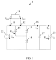
- FIG. 1 illustrates a hybrid switched-mode step-down converter 1 in accordance with the present disclosure.
- the converter 1 is suitable for an LED load 23 connectable to an output port of the converter 1.
- the converter 1 comprises a first decoupling element 11, a second decoupling element 12, a third decoupling element 13 and a fourth decoupling element 14 connected in series across an input port of the converter 1 connectable to a DC power source 22.
- a voltage supplied by the DC power source 22 is identified as U 22 .
- the converter 1 further comprises a control logic 18 configured to operate the respective decoupling element 11 - 14 provided that this is warranted, as will be explained below in more detail.
- the control logic 18 may form part of an integrated circuit, preferably a monolithically integrated circuit.
- the first decoupling element 11 and the second decoupling element 12 may respectively comprise an electronic switch, as shown in FIG. 1 .
- the control logic 18 is configured to operate the respective decoupling element 11, 12.
- Drive currents of the respective decoupling element 11 - 12 are identified as I G11 and I G12 , respectively.
- the third decoupling element 13 and the fourth decoupling element 14 may respectively comprise a diode, as shown in FIG. 1 , in which case the control logic 18 is not configured to operate the respective decoupling element 13, 14.
- the diodes arranged to prevent shorting the DC voltage source (i.e., the cathodes oriented towards a high-side potential, and the anodes oriented towards a low-side potential).
- the third decoupling element 13 and the fourth decoupling element 14 may also comprise respective electronic switches, in which case the control logic 18 may further be configured to operate the respective decoupling element 13, 14. More specifically, the control logic 18 may be configured to open the third decoupling element 13 and/or the fourth decoupling element 14 in dependence of respective opening states of the first decoupling element 11 and the second decoupling element 12. In other words, the third decoupling element 13 and the fourth decoupling element 14 may be operated in accordance with a well-known synchronous operation for reduction of switching loss.
- the converter 1 further comprises a first capacitive storage element 15 (flying capacitor) connected in parallel to the series connection of the second decoupling element 12 and the third decoupling element 13.
- a voltage across the first capacitive storage element 15 is identified as U 15 .
- the converter 1 further comprises an inductive storage element 16 (having an inductance of L 16 ) and a second capacitive storage element 17 (smoothing capacitor) connected in parallel to the series connection of the third decoupling element 13 and the fourth decoupling element 14.
- the second capacitive storage element 17 is connected in parallel to the output port of the converter 1 connectable to the LED load 23.
- a current of the inductive storage element 16 is identified as I 16
- a load current of the LED load 23 is identified as I 23
- a voltage across the LED load 23 is identified as U 23 .
- the control logic 18 is configured to alternatingly open the first decoupling element 11 and the second decoupling element 12 in accordance with a modulation frequency with an intermediate time lag, wherein in a first dimming range of the LED load 23, the control logic 18 is configured to preserve a duration of the time lag; and in a second dimming range of the LED load 23, the control logic 18 is configured to modulate the duration of the time lag.
- FIGs. 2 - 5 illustrate operation phases of the converter of FIG. 1 .
- both the first decoupling element 11 and the second decoupling element 12 are operated in a closed (conducting) state.
- the DC power source 22 directly charges the inductive storage element 16.
- the first decoupling element 11 is maintained in the closed (conducting) state, and the second decoupling element 12 is operated in an open (non-conducting) state.
- the DC power source 22 now directly charges the first capacitive storage element 15, and a resonant current between the first capacitive storage element 15 and the inductive storage element 16 emerges until the latter is charged.
- the current I 16 of the inductive storage element 16 decreases until it reaches zero.
- a maximum drop of the voltage U 15 across the first capacitive storage element 15 is clamped by the fourth decoupling element 14. So when increasing a capacitance of the first capacitive storage element 15, the current I 16 of the inductive storage element 16 increases as long as the voltage U 15 across the first capacitive storage element 15 is smaller as or equal to U 22 .
- a third operation phase depicted in FIG. 4 the first decoupling element 11 is maintained in the closed (conducting) state and the second decoupling element 12 is operated in the closed (conducting) state. That is to say, with reference to the operating states of the first and second decoupling elements 11, 12, the third operation phase corresponds to the first operation phase, but the state of charge of the first capacitive storage element 15 has changed. Again, the DC power source 22 directly charges the inductive storage element 16.
- a fourth operation phase depicted in FIG. 5 the first decoupling element 11 is operated in the open (non-conducting) state, and the second decoupling element 12 is maintained in the closed (conducting) state state. Therefore, the first capacitive storage element 15 is discharged via the inductive storage element 16, and the converter 1 completes the quasi-resonant cycle started in the second operation phase.
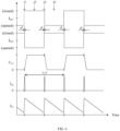
- FIG. 6 illustrates waveforms of the operation phases of the converter of FIG. 1 .
- both the first decoupling element 11 and the second decoupling element 12 are operated in a closed (conducting) state (i.e., the drive currents I G11 and I G12 are non-zero).
- the DC power source 22 directly charges the inductive storage element 16.
- the current I 16 of the inductive storage element 16 therefore increases almost linearly over time (note the sharply rising edge of current I 16 ).
- the first decoupling element 11 is maintained in the closed (conducting) state (the drive current I G11 remains non-zero), and the second decoupling element 12 is operated in an open (non-conducting) state (the drive current I G12 becomes zero).
- the DC power source 22 now directly charges the first capacitive storage element 15 (note the rising edge of voltage U 15 ), and a resonant current between the first capacitive storage element 15 and the inductive storage element 16 emerges until the former is charged.
- the current I 16 of the inductive storage element 16 decreases until it reaches zero (note the sharply falling edge of current I 16 ).
- the first decoupling element 11 is maintained in the closed (conducting) state (the drive current I G11 remains non-zero) and the second decoupling element 12 is operated in the closed (conducting) state (the drive current I G12 becomes non-zero).
- the DC power source 22 directly charges the inductive storage element 16, and the current I 16 of the inductive storage element 16 increases almost linearly over time (note the sharply rising edge of current I 16 ).
- the first decoupling element 11 is operated in the open (non-conducting) state (the drive current I G11 becomes zero), and the second decoupling element 12 is maintained in the closed (conducting) state (the drive current I G12 remains non-zero). Therefore, the first capacitive storage element 15 is discharged (note the falling edge of voltage U 15 ) via the inductive storage element 16, and the converter 1 completes the quasi-resonant cycle started in the second operation phase (note the sharply falling edge of current I 16 ).
- control logic 18 is configured to alternatingly open the first decoupling element 11 and the second decoupling element 12 in accordance with the modulation frequency indicated as ⁇ in FIG. 6 .
- An average value of the current I 23 of the LED load may be increased or decreased by increasing or decreasing the modulation frequency. That is to say, the LED load may be dimmed by decreasing the modulation frequency.
- the frequency ⁇ may be fixated and the average value of the load current I 23 may further be reduced by shortening the duration of the intermediate time lag, which is indicated as d in FIG. 6 .
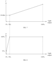
- FIG. 7 illustrates a modulation frequency of the converter of FIG. 1 as a function of light output
- FIG. 8 illustrates a duration of the first and third operating phases of the converter of FIG. 1 as a function of light output.
- FIG. 7 shows the first and second dimming ranges of the LED load 23.
- the first (moderate) dimming range may extend from a full i.e., 100% light output of the LED load 23 to a reduced (X%) light output of the LED load 23 achieved at a minimum modulation frequency.
- the minimum modulation frequency may comprise a frequency being inaudible to a human ear, such as 30 kHz, more preferably 25 kHz, and most preferably 20 kHz.
- the second (more extensive) dimming range may extend from the reduced (X%) light output of the LED load 23 to a minimum light output of the LED load 23 achieved at a minimum duration of the time lag.
- the minimum light output of the LED load 23 may comprise 1% of the full light output of the LED load 23.
- control logic 18 is configured to alternatingly open the first decoupling element 11 and the second decoupling element 12 in accordance with the modulation frequency ⁇ .
- the control logic 18 is configured to perform the frequency modulation and to maintain a duration d of the intermediate time lag between alternating decoupling actions of the serially connected first and second decoupling elements 11, 12 constant. Therefore, the LED load 23 may be dimmed by linearly decreasing the modulation frequency f (see FIG. 7 ) and keeping the duration of the intermediate time lag d constant (see FIG. 8 ).
- control logic 18 is configured to maintain the frequency modulation constant and to modulate the duration d of the intermediate time lag.
- the LED load 23 may be dimmed further by linearly decreasing the duration d of the intermediate time lag (see FIG. 8 ) and keeping the modulation frequency ⁇ constant (see FIG. 7 ).
- the modulation frequencyf may be decreased down to a minimum frequency of e.g. 20 kHz, which defines the X% point in FIG. 7 .
- the duration d of the intermediate time lag requires reduction as well.
- the duration d may be decreased down to the Y% point in FIG. 8 , which corresponds to the minimum (1%) light output of the LED load 23.
- FIG. 9 illustrates a lighting system 2 in accordance with the present disclosure.
- the lighting system 2 comprises a lighting bus 21.
- the lighting system 2 further comprises a DC power source 22 being configured to supply DC power to the lighting bus 21.
- the lighting system 2 further comprises a number of hybrid switched-mode converters 1 of the first aspect or any of its implementations.
- the respective converter is connected to the lighting bus 21, and configured to supply DC power to a respective LED load 23 off the lighting bus 21.
- FIG. 10 illustrates a flow chart of a method 3 in accordance with the present disclosure of operating the converter of FIG. 1 .
- the method 3 is suitable of operating a hybrid switched-mode converter 1 of the first aspect or any of its implementations.
- the method 3 comprises a step of alternatingly opening 31 the first decoupling element 11 and the second decoupling element 12 with an intermediate time lag in accordance with a modulation frequency.
- the method 3 further comprises a step of preserving 32 a duration of the time lag in a first dimming range of the LED load 23.
- the method 3 further comprises a step of modulating 33 the duration of the time lag in a second dimming range of the LED load 23.
Landscapes
- Engineering & Computer Science (AREA)
- Power Engineering (AREA)
- Circuit Arrangement For Electric Light Sources In General (AREA)
Priority Applications (2)
| Application Number | Priority Date | Filing Date | Title |
|---|---|---|---|
| EP21214714.4A EP4199331B1 (de) | 2021-12-15 | 2021-12-15 | Hybrider schaltwandler, verfahren zu dessen betrieb und beleuchtungssystem |
| PCT/EP2022/083229 WO2023110360A1 (en) | 2021-12-15 | 2022-11-25 | Hybrid switched-mode converter, method of operating the same, and lighting system |
Applications Claiming Priority (1)
| Application Number | Priority Date | Filing Date | Title |
|---|---|---|---|
| EP21214714.4A EP4199331B1 (de) | 2021-12-15 | 2021-12-15 | Hybrider schaltwandler, verfahren zu dessen betrieb und beleuchtungssystem |
Publications (2)
| Publication Number | Publication Date |
|---|---|
| EP4199331A1 true EP4199331A1 (de) | 2023-06-21 |
| EP4199331B1 EP4199331B1 (de) | 2025-01-29 |
Family
ID=78916892
Family Applications (1)
| Application Number | Title | Priority Date | Filing Date |
|---|---|---|---|
| EP21214714.4A Active EP4199331B1 (de) | 2021-12-15 | 2021-12-15 | Hybrider schaltwandler, verfahren zu dessen betrieb und beleuchtungssystem |
Country Status (2)
| Country | Link |
|---|---|
| EP (1) | EP4199331B1 (de) |
| WO (1) | WO2023110360A1 (de) |
-
2021
- 2021-12-15 EP EP21214714.4A patent/EP4199331B1/de active Active
-
2022
- 2022-11-25 WO PCT/EP2022/083229 patent/WO2023110360A1/en not_active Ceased
Non-Patent Citations (1)
| Title |
|---|
| JUAN C CASTELLANOS ET AL: "Dimmable integrated CMOS LED driver based on a resonant DC/DC hybrid-switched capacitor converter", INTERNATIONAL JOURNAL OF CIRCUIT THEORY AND APPLICATIONS, JOHN WILEY & SONS, INC, HOBOKEN, USA, vol. 46, no. 8, 21 June 2018 (2018-06-21), pages 1485 - 1502, XP071448710, ISSN: 0098-9886, DOI: 10.1002/CTA.2512 * |
Also Published As
| Publication number | Publication date |
|---|---|
| EP4199331B1 (de) | 2025-01-29 |
| WO2023110360A1 (en) | 2023-06-22 |
Similar Documents
| Publication | Publication Date | Title |
|---|---|---|
| US10651731B1 (en) | Zero voltage switching of interleaved switched-capacitor converters | |
| US6429604B2 (en) | Power feedback power factor correction scheme for multiple lamp operation | |
| US10356861B2 (en) | Constant output current LED driver | |
| MX2010005314A (es) | Balastro electronico con convertidor dc-dc (corriente directa-corriente directa) para correccion de factor de energia escalonada ascendente/descendente apropiado para aplicaciones de alto voltaje de entrada. | |
| US20040151009A1 (en) | Power factor correction circuit | |
| EP0440245A2 (de) | Stromversorgungsschaltung | |
| KR20090017426A (ko) | 인버터 | |
| WO2021209613A1 (en) | A dc-dc converter assembly | |
| JP2001037212A (ja) | 低電圧入力dc−dcコンバータ | |
| US20230318453A1 (en) | Control of two-stage dc-dc converter | |
| US12261517B2 (en) | H-bridge circuit with bootstrap capacitor gate drive charging circuit | |
| JP2013516153A (ja) | 接地可能dc/dcコンバータ | |
| US6489730B2 (en) | Discharge-lamp illumination circuit | |
| CN1387307A (zh) | 自激振荡同步升压变换器 | |
| US6225755B1 (en) | High power factor electronic ballast with simplified circuit topology | |
| KR102858579B1 (ko) | 브릿지리스 역률개선 컨버터 | |
| US11205969B2 (en) | Inverter device configured to operate in a CCM and sequentially operate in buck and boost phases | |
| KR101030776B1 (ko) | 승압형 직류/직류 변환기 | |
| EP4199331B1 (de) | Hybrider schaltwandler, verfahren zu dessen betrieb und beleuchtungssystem | |
| US7193373B2 (en) | Electronic ballast having a converter which can continue to operate in the event of lamp failure | |
| US6707261B2 (en) | Discharge lamp lighting circuit | |
| US12107520B2 (en) | Driving circuit and driving method | |
| WO2008064767A1 (en) | Power supply system for a vehicle, and method | |
| US10158284B2 (en) | PFC with stacked half-bridges on DC side of rectifier | |
| Ghumman et al. | High gain interleaved stacked boost converter |
Legal Events
| Date | Code | Title | Description |
|---|---|---|---|
| PUAI | Public reference made under article 153(3) epc to a published international application that has entered the european phase |
Free format text: ORIGINAL CODE: 0009012 |
|
| STAA | Information on the status of an ep patent application or granted ep patent |
Free format text: STATUS: THE APPLICATION HAS BEEN PUBLISHED |
|
| AK | Designated contracting states |
Kind code of ref document: A1 Designated state(s): AL AT BE BG CH CY CZ DE DK EE ES FI FR GB GR HR HU IE IS IT LI LT LU LV MC MK MT NL NO PL PT RO RS SE SI SK SM TR |
|
| STAA | Information on the status of an ep patent application or granted ep patent |
Free format text: STATUS: REQUEST FOR EXAMINATION WAS MADE |
|
| 17P | Request for examination filed |
Effective date: 20230706 |
|
| RBV | Designated contracting states (corrected) |
Designated state(s): AL AT BE BG CH CY CZ DE DK EE ES FI FR GB GR HR HU IE IS IT LI LT LU LV MC MK MT NL NO PL PT RO RS SE SI SK SM TR |
|
| GRAP | Despatch of communication of intention to grant a patent |
Free format text: ORIGINAL CODE: EPIDOSNIGR1 |
|
| STAA | Information on the status of an ep patent application or granted ep patent |
Free format text: STATUS: GRANT OF PATENT IS INTENDED |
|
| RIC1 | Information provided on ipc code assigned before grant |
Ipc: H02M 3/156 20060101ALI20240830BHEP Ipc: H05B 45/335 20200101ALI20240830BHEP Ipc: H05B 45/3725 20200101ALI20240830BHEP Ipc: H02M 3/07 20060101ALI20240830BHEP Ipc: H02M 1/00 20060101AFI20240830BHEP |
|
| INTG | Intention to grant announced |
Effective date: 20240924 |
|
| GRAS | Grant fee paid |
Free format text: ORIGINAL CODE: EPIDOSNIGR3 |
|
| GRAA | (expected) grant |
Free format text: ORIGINAL CODE: 0009210 |
|
| STAA | Information on the status of an ep patent application or granted ep patent |
Free format text: STATUS: THE PATENT HAS BEEN GRANTED |
|
| P01 | Opt-out of the competence of the unified patent court (upc) registered |
Free format text: CASE NUMBER: APP_63544/2024 Effective date: 20241129 |
|
| AK | Designated contracting states |
Kind code of ref document: B1 Designated state(s): AL AT BE BG CH CY CZ DE DK EE ES FI FR GB GR HR HU IE IS IT LI LT LU LV MC MK MT NL NO PL PT RO RS SE SI SK SM TR |
|
| REG | Reference to a national code |
Ref country code: GB Ref legal event code: FG4D |
|
| REG | Reference to a national code |
Ref country code: CH Ref legal event code: EP |
|
| REG | Reference to a national code |
Ref country code: DE Ref legal event code: R096 Ref document number: 602021025349 Country of ref document: DE |
|
| REG | Reference to a national code |
Ref country code: IE Ref legal event code: FG4D Ref country code: DE Ref legal event code: R084 Ref document number: 602021025349 Country of ref document: DE |
|
| REG | Reference to a national code |
Ref country code: NL Ref legal event code: MP Effective date: 20250129 |
|
| PG25 | Lapsed in a contracting state [announced via postgrant information from national office to epo] |
Ref country code: NL Free format text: LAPSE BECAUSE OF FAILURE TO SUBMIT A TRANSLATION OF THE DESCRIPTION OR TO PAY THE FEE WITHIN THE PRESCRIBED TIME-LIMIT Effective date: 20250129 |
|
| PG25 | Lapsed in a contracting state [announced via postgrant information from national office to epo] |
Ref country code: RS Free format text: LAPSE BECAUSE OF FAILURE TO SUBMIT A TRANSLATION OF THE DESCRIPTION OR TO PAY THE FEE WITHIN THE PRESCRIBED TIME-LIMIT Effective date: 20250429 |
|
| PG25 | Lapsed in a contracting state [announced via postgrant information from national office to epo] |
Ref country code: FI Free format text: LAPSE BECAUSE OF FAILURE TO SUBMIT A TRANSLATION OF THE DESCRIPTION OR TO PAY THE FEE WITHIN THE PRESCRIBED TIME-LIMIT Effective date: 20250129 |
|
| PG25 | Lapsed in a contracting state [announced via postgrant information from national office to epo] |
Ref country code: PL Free format text: LAPSE BECAUSE OF FAILURE TO SUBMIT A TRANSLATION OF THE DESCRIPTION OR TO PAY THE FEE WITHIN THE PRESCRIBED TIME-LIMIT Effective date: 20250129 |
|
| PG25 | Lapsed in a contracting state [announced via postgrant information from national office to epo] |
Ref country code: ES Free format text: LAPSE BECAUSE OF FAILURE TO SUBMIT A TRANSLATION OF THE DESCRIPTION OR TO PAY THE FEE WITHIN THE PRESCRIBED TIME-LIMIT Effective date: 20250129 |
|
| REG | Reference to a national code |
Ref country code: LT Ref legal event code: MG9D |
|
| PG25 | Lapsed in a contracting state [announced via postgrant information from national office to epo] |
Ref country code: IS Free format text: LAPSE BECAUSE OF FAILURE TO SUBMIT A TRANSLATION OF THE DESCRIPTION OR TO PAY THE FEE WITHIN THE PRESCRIBED TIME-LIMIT Effective date: 20250529 Ref country code: NO Free format text: LAPSE BECAUSE OF FAILURE TO SUBMIT A TRANSLATION OF THE DESCRIPTION OR TO PAY THE FEE WITHIN THE PRESCRIBED TIME-LIMIT Effective date: 20250429 |
|
| REG | Reference to a national code |
Ref country code: AT Ref legal event code: MK05 Ref document number: 1764463 Country of ref document: AT Kind code of ref document: T Effective date: 20250129 |
|
| PG25 | Lapsed in a contracting state [announced via postgrant information from national office to epo] |
Ref country code: HR Free format text: LAPSE BECAUSE OF FAILURE TO SUBMIT A TRANSLATION OF THE DESCRIPTION OR TO PAY THE FEE WITHIN THE PRESCRIBED TIME-LIMIT Effective date: 20250129 |
|
| PG25 | Lapsed in a contracting state [announced via postgrant information from national office to epo] |
Ref country code: PT Free format text: LAPSE BECAUSE OF FAILURE TO SUBMIT A TRANSLATION OF THE DESCRIPTION OR TO PAY THE FEE WITHIN THE PRESCRIBED TIME-LIMIT Effective date: 20250529 Ref country code: LV Free format text: LAPSE BECAUSE OF FAILURE TO SUBMIT A TRANSLATION OF THE DESCRIPTION OR TO PAY THE FEE WITHIN THE PRESCRIBED TIME-LIMIT Effective date: 20250129 |
|
| PG25 | Lapsed in a contracting state [announced via postgrant information from national office to epo] |
Ref country code: BG Free format text: LAPSE BECAUSE OF FAILURE TO SUBMIT A TRANSLATION OF THE DESCRIPTION OR TO PAY THE FEE WITHIN THE PRESCRIBED TIME-LIMIT Effective date: 20250129 Ref country code: GR Free format text: LAPSE BECAUSE OF FAILURE TO SUBMIT A TRANSLATION OF THE DESCRIPTION OR TO PAY THE FEE WITHIN THE PRESCRIBED TIME-LIMIT Effective date: 20250430 |
|
| PG25 | Lapsed in a contracting state [announced via postgrant information from national office to epo] |
Ref country code: AT Free format text: LAPSE BECAUSE OF FAILURE TO SUBMIT A TRANSLATION OF THE DESCRIPTION OR TO PAY THE FEE WITHIN THE PRESCRIBED TIME-LIMIT Effective date: 20250129 |
|
| PG25 | Lapsed in a contracting state [announced via postgrant information from national office to epo] |
Ref country code: SE Free format text: LAPSE BECAUSE OF FAILURE TO SUBMIT A TRANSLATION OF THE DESCRIPTION OR TO PAY THE FEE WITHIN THE PRESCRIBED TIME-LIMIT Effective date: 20250129 |
|
| PG25 | Lapsed in a contracting state [announced via postgrant information from national office to epo] |
Ref country code: SM Free format text: LAPSE BECAUSE OF FAILURE TO SUBMIT A TRANSLATION OF THE DESCRIPTION OR TO PAY THE FEE WITHIN THE PRESCRIBED TIME-LIMIT Effective date: 20250129 |
|
| PG25 | Lapsed in a contracting state [announced via postgrant information from national office to epo] |
Ref country code: DK Free format text: LAPSE BECAUSE OF FAILURE TO SUBMIT A TRANSLATION OF THE DESCRIPTION OR TO PAY THE FEE WITHIN THE PRESCRIBED TIME-LIMIT Effective date: 20250129 |
|
| PG25 | Lapsed in a contracting state [announced via postgrant information from national office to epo] |
Ref country code: IT Free format text: LAPSE BECAUSE OF FAILURE TO SUBMIT A TRANSLATION OF THE DESCRIPTION OR TO PAY THE FEE WITHIN THE PRESCRIBED TIME-LIMIT Effective date: 20250129 |
|
| PG25 | Lapsed in a contracting state [announced via postgrant information from national office to epo] |
Ref country code: EE Free format text: LAPSE BECAUSE OF FAILURE TO SUBMIT A TRANSLATION OF THE DESCRIPTION OR TO PAY THE FEE WITHIN THE PRESCRIBED TIME-LIMIT Effective date: 20250129 Ref country code: CZ Free format text: LAPSE BECAUSE OF FAILURE TO SUBMIT A TRANSLATION OF THE DESCRIPTION OR TO PAY THE FEE WITHIN THE PRESCRIBED TIME-LIMIT Effective date: 20250129 |
|
| PG25 | Lapsed in a contracting state [announced via postgrant information from national office to epo] |
Ref country code: RO Free format text: LAPSE BECAUSE OF FAILURE TO SUBMIT A TRANSLATION OF THE DESCRIPTION OR TO PAY THE FEE WITHIN THE PRESCRIBED TIME-LIMIT Effective date: 20250129 |
|
| PG25 | Lapsed in a contracting state [announced via postgrant information from national office to epo] |
Ref country code: SK Free format text: LAPSE BECAUSE OF FAILURE TO SUBMIT A TRANSLATION OF THE DESCRIPTION OR TO PAY THE FEE WITHIN THE PRESCRIBED TIME-LIMIT Effective date: 20250129 |
|
| REG | Reference to a national code |
Ref country code: DE Ref legal event code: R097 Ref document number: 602021025349 Country of ref document: DE |
|
| PLBE | No opposition filed within time limit |
Free format text: ORIGINAL CODE: 0009261 |
|
| STAA | Information on the status of an ep patent application or granted ep patent |
Free format text: STATUS: NO OPPOSITION FILED WITHIN TIME LIMIT |
|
| 26N | No opposition filed |
Effective date: 20251030 |
|
| PGFP | Annual fee paid to national office [announced via postgrant information from national office to epo] |
Ref country code: GB Payment date: 20251223 Year of fee payment: 5 |
|
| PGFP | Annual fee paid to national office [announced via postgrant information from national office to epo] |
Ref country code: FR Payment date: 20251223 Year of fee payment: 5 |
|
| PGFP | Annual fee paid to national office [announced via postgrant information from national office to epo] |
Ref country code: DE Payment date: 20251229 Year of fee payment: 5 |