EP4199085A1 - Semiconductor structure and fabrication method therefor - Google Patents
Semiconductor structure and fabrication method therefor Download PDFInfo
- Publication number
- EP4199085A1 EP4199085A1 EP22865907.4A EP22865907A EP4199085A1 EP 4199085 A1 EP4199085 A1 EP 4199085A1 EP 22865907 A EP22865907 A EP 22865907A EP 4199085 A1 EP4199085 A1 EP 4199085A1
- Authority
- EP
- European Patent Office
- Prior art keywords
- layer
- substrate
- conductive layer
- semiconductor structure
- contact
- Prior art date
- Legal status (The legal status is an assumption and is not a legal conclusion. Google has not performed a legal analysis and makes no representation as to the accuracy of the status listed.)
- Pending
Links
- 239000004065 semiconductor Substances 0.000 title claims abstract description 56
- 238000004519 manufacturing process Methods 0.000 title claims abstract description 28
- 238000000034 method Methods 0.000 title description 3
- 239000000758 substrate Substances 0.000 claims abstract description 87
- 229910052751 metal Inorganic materials 0.000 claims abstract description 25
- 239000002184 metal Substances 0.000 claims abstract description 25
- 229920002120 photoresistant polymer Polymers 0.000 claims description 30
- 239000000463 material Substances 0.000 claims description 18
- CWQXQMHSOZUFJS-UHFFFAOYSA-N molybdenum disulfide Chemical compound S=[Mo]=S CWQXQMHSOZUFJS-UHFFFAOYSA-N 0.000 claims description 13
- 230000000717 retained effect Effects 0.000 claims description 12
- 229910052797 bismuth Inorganic materials 0.000 claims description 8
- JCXGWMGPZLAOME-UHFFFAOYSA-N bismuth atom Chemical compound [Bi] JCXGWMGPZLAOME-UHFFFAOYSA-N 0.000 claims description 8
- 238000000151 deposition Methods 0.000 claims description 5
- 238000005530 etching Methods 0.000 claims description 5
- 238000002955 isolation Methods 0.000 claims description 2
- 238000010586 diagram Methods 0.000 description 32
- 239000003990 capacitor Substances 0.000 description 12
- VYPSYNLAJGMNEJ-UHFFFAOYSA-N Silicium dioxide Chemical compound O=[Si]=O VYPSYNLAJGMNEJ-UHFFFAOYSA-N 0.000 description 5
- 230000000694 effects Effects 0.000 description 5
- 229910052814 silicon oxide Inorganic materials 0.000 description 4
- XUIMIQQOPSSXEZ-UHFFFAOYSA-N Silicon Chemical compound [Si] XUIMIQQOPSSXEZ-UHFFFAOYSA-N 0.000 description 3
- 230000008021 deposition Effects 0.000 description 3
- 238000005137 deposition process Methods 0.000 description 3
- 230000002093 peripheral effect Effects 0.000 description 3
- 229910052710 silicon Inorganic materials 0.000 description 3
- 239000010703 silicon Substances 0.000 description 3
- 229910052581 Si3N4 Inorganic materials 0.000 description 2
- 238000000231 atomic layer deposition Methods 0.000 description 2
- 230000004888 barrier function Effects 0.000 description 2
- 239000000969 carrier Substances 0.000 description 2
- 238000005229 chemical vapour deposition Methods 0.000 description 2
- 238000001312 dry etching Methods 0.000 description 2
- 230000005669 field effect Effects 0.000 description 2
- 239000011810 insulating material Substances 0.000 description 2
- 239000012212 insulator Substances 0.000 description 2
- 229910052982 molybdenum disulfide Inorganic materials 0.000 description 2
- 238000005240 physical vapour deposition Methods 0.000 description 2
- 230000008569 process Effects 0.000 description 2
- HQVNEWCFYHHQES-UHFFFAOYSA-N silicon nitride Chemical compound N12[Si]34N5[Si]62N3[Si]51N64 HQVNEWCFYHHQES-UHFFFAOYSA-N 0.000 description 2
- 238000006467 substitution reaction Methods 0.000 description 2
- 238000001039 wet etching Methods 0.000 description 2
- JBRZTFJDHDCESZ-UHFFFAOYSA-N AsGa Chemical compound [As]#[Ga] JBRZTFJDHDCESZ-UHFFFAOYSA-N 0.000 description 1
- 229910002601 GaN Inorganic materials 0.000 description 1
- 229910001218 Gallium arsenide Inorganic materials 0.000 description 1
- JMASRVWKEDWRBT-UHFFFAOYSA-N Gallium nitride Chemical compound [Ga]#N JMASRVWKEDWRBT-UHFFFAOYSA-N 0.000 description 1
- 241001640034 Heteropterys Species 0.000 description 1
- 229910000577 Silicon-germanium Inorganic materials 0.000 description 1
- LEVVHYCKPQWKOP-UHFFFAOYSA-N [Si].[Ge] Chemical compound [Si].[Ge] LEVVHYCKPQWKOP-UHFFFAOYSA-N 0.000 description 1
- 230000009286 beneficial effect Effects 0.000 description 1
- 229910052732 germanium Inorganic materials 0.000 description 1
- GNPVGFCGXDBREM-UHFFFAOYSA-N germanium atom Chemical compound [Ge] GNPVGFCGXDBREM-UHFFFAOYSA-N 0.000 description 1
- 230000004048 modification Effects 0.000 description 1
- 238000012986 modification Methods 0.000 description 1
- 238000005498 polishing Methods 0.000 description 1
- 230000000750 progressive effect Effects 0.000 description 1
- 239000000126 substance Substances 0.000 description 1
- 229910052723 transition metal Inorganic materials 0.000 description 1
- -1 transition metal sulfur compounds Chemical class 0.000 description 1
Images


Classifications
-
- H—ELECTRICITY
- H10—SEMICONDUCTOR DEVICES; ELECTRIC SOLID-STATE DEVICES NOT OTHERWISE PROVIDED FOR
- H10B—ELECTRONIC MEMORY DEVICES
- H10B12/00—Dynamic random access memory [DRAM] devices
- H10B12/30—DRAM devices comprising one-transistor - one-capacitor [1T-1C] memory cells
-
- H—ELECTRICITY
- H01—ELECTRIC ELEMENTS
- H01L—SEMICONDUCTOR DEVICES NOT COVERED BY CLASS H10
- H01L29/00—Semiconductor devices adapted for rectifying, amplifying, oscillating or switching, or capacitors or resistors with at least one potential-jump barrier or surface barrier, e.g. PN junction depletion layer or carrier concentration layer; Details of semiconductor bodies or of electrodes thereof ; Multistep manufacturing processes therefor
- H01L29/40—Electrodes ; Multistep manufacturing processes therefor
- H01L29/43—Electrodes ; Multistep manufacturing processes therefor characterised by the materials of which they are formed
-
- H—ELECTRICITY
- H01—ELECTRIC ELEMENTS
- H01L—SEMICONDUCTOR DEVICES NOT COVERED BY CLASS H10
- H01L29/00—Semiconductor devices adapted for rectifying, amplifying, oscillating or switching, or capacitors or resistors with at least one potential-jump barrier or surface barrier, e.g. PN junction depletion layer or carrier concentration layer; Details of semiconductor bodies or of electrodes thereof ; Multistep manufacturing processes therefor
- H01L29/66—Types of semiconductor device ; Multistep manufacturing processes therefor
- H01L29/68—Types of semiconductor device ; Multistep manufacturing processes therefor controllable by only the electric current supplied, or only the electric potential applied, to an electrode which does not carry the current to be rectified, amplified or switched
- H01L29/76—Unipolar devices, e.g. field effect transistors
- H01L29/772—Field effect transistors
- H01L29/78—Field effect transistors with field effect produced by an insulated gate
- H01L29/7827—Vertical transistors
-
- H—ELECTRICITY
- H01—ELECTRIC ELEMENTS
- H01L—SEMICONDUCTOR DEVICES NOT COVERED BY CLASS H10
- H01L29/00—Semiconductor devices adapted for rectifying, amplifying, oscillating or switching, or capacitors or resistors with at least one potential-jump barrier or surface barrier, e.g. PN junction depletion layer or carrier concentration layer; Details of semiconductor bodies or of electrodes thereof ; Multistep manufacturing processes therefor
- H01L29/66—Types of semiconductor device ; Multistep manufacturing processes therefor
- H01L29/68—Types of semiconductor device ; Multistep manufacturing processes therefor controllable by only the electric current supplied, or only the electric potential applied, to an electrode which does not carry the current to be rectified, amplified or switched
- H01L29/76—Unipolar devices, e.g. field effect transistors
- H01L29/772—Field effect transistors
- H01L29/78—Field effect transistors with field effect produced by an insulated gate
- H01L29/786—Thin film transistors, i.e. transistors with a channel being at least partly a thin film
- H01L29/78642—Vertical transistors
-
- H—ELECTRICITY
- H10—SEMICONDUCTOR DEVICES; ELECTRIC SOLID-STATE DEVICES NOT OTHERWISE PROVIDED FOR
- H10B—ELECTRONIC MEMORY DEVICES
- H10B12/00—Dynamic random access memory [DRAM] devices
- H10B12/01—Manufacture or treatment
- H10B12/02—Manufacture or treatment for one transistor one-capacitor [1T-1C] memory cells
- H10B12/05—Making the transistor
-
- H—ELECTRICITY
- H10—SEMICONDUCTOR DEVICES; ELECTRIC SOLID-STATE DEVICES NOT OTHERWISE PROVIDED FOR
- H10B—ELECTRONIC MEMORY DEVICES
- H10B12/00—Dynamic random access memory [DRAM] devices
- H10B12/30—DRAM devices comprising one-transistor - one-capacitor [1T-1C] memory cells
- H10B12/48—Data lines or contacts therefor
- H10B12/482—Bit lines
-
- H—ELECTRICITY
- H10—SEMICONDUCTOR DEVICES; ELECTRIC SOLID-STATE DEVICES NOT OTHERWISE PROVIDED FOR
- H10B—ELECTRONIC MEMORY DEVICES
- H10B12/00—Dynamic random access memory [DRAM] devices
- H10B12/30—DRAM devices comprising one-transistor - one-capacitor [1T-1C] memory cells
- H10B12/48—Data lines or contacts therefor
- H10B12/488—Word lines
-
- H—ELECTRICITY
- H01—ELECTRIC ELEMENTS
- H01L—SEMICONDUCTOR DEVICES NOT COVERED BY CLASS H10
- H01L27/00—Devices consisting of a plurality of semiconductor or other solid-state components formed in or on a common substrate
- H01L27/02—Devices consisting of a plurality of semiconductor or other solid-state components formed in or on a common substrate including semiconductor components specially adapted for rectifying, oscillating, amplifying or switching and having at least one potential-jump barrier or surface barrier; including integrated passive circuit elements with at least one potential-jump barrier or surface barrier
- H01L27/12—Devices consisting of a plurality of semiconductor or other solid-state components formed in or on a common substrate including semiconductor components specially adapted for rectifying, oscillating, amplifying or switching and having at least one potential-jump barrier or surface barrier; including integrated passive circuit elements with at least one potential-jump barrier or surface barrier the substrate being other than a semiconductor body, e.g. an insulating body
- H01L27/1203—Devices consisting of a plurality of semiconductor or other solid-state components formed in or on a common substrate including semiconductor components specially adapted for rectifying, oscillating, amplifying or switching and having at least one potential-jump barrier or surface barrier; including integrated passive circuit elements with at least one potential-jump barrier or surface barrier the substrate being other than a semiconductor body, e.g. an insulating body the substrate comprising an insulating body on a semiconductor body, e.g. SOI
-
- H—ELECTRICITY
- H10—SEMICONDUCTOR DEVICES; ELECTRIC SOLID-STATE DEVICES NOT OTHERWISE PROVIDED FOR
- H10B—ELECTRONIC MEMORY DEVICES
- H10B12/00—Dynamic random access memory [DRAM] devices
- H10B12/30—DRAM devices comprising one-transistor - one-capacitor [1T-1C] memory cells
- H10B12/31—DRAM devices comprising one-transistor - one-capacitor [1T-1C] memory cells having a storage electrode stacked over the transistor
- H10B12/315—DRAM devices comprising one-transistor - one-capacitor [1T-1C] memory cells having a storage electrode stacked over the transistor with the capacitor higher than a bit line
Landscapes
- Engineering & Computer Science (AREA)
- Microelectronics & Electronic Packaging (AREA)
- Power Engineering (AREA)
- Physics & Mathematics (AREA)
- Ceramic Engineering (AREA)
- Condensed Matter Physics & Semiconductors (AREA)
- General Physics & Mathematics (AREA)
- Computer Hardware Design (AREA)
- Manufacturing & Machinery (AREA)
- Semiconductor Memories (AREA)
- Internal Circuitry In Semiconductor Integrated Circuit Devices (AREA)
Abstract
Description
- The present disclosure claims the priority to
Chinese Patent Application 202111231509.3, titled "SEMICONDUCTOR STRUCTURE AND MANUFACTURING METHOD THEREOF", filed with the China National Intellectual Property Administration (CNIPA) on October 22, 2021 - The present application relates to the technical field of semiconductors, and in particular to a semiconductor structure and a manufacturing method thereof.
- The semiconductor structure may include memory cells. The memory cell usually includes a transistor and a capacitor electrically connected to the transistor. The capacitor stores data information, and the transistor controls the reading and writing of data information in the capacitor. The gate of the transistor is electrically connected to a word line (WL), and the on and off of the transistor is controlled by the voltage on the WL. One of a source and a drain of the transistor is electrically connected to a bit line (BL), and the other of the source and the drain is electrically connected to the capacitor. Data information is stored or outputted by using the BL.
- As a size of the semiconductor structure becomes more miniaturized, gate-all-around (GAA) transistors are usually used. In the related art, the GAA transistor includes a first conductive layer, a channel region, and a second conductive layer that are stacked sequentially. One of the first conductive layer and the second conductive layer is a source, and the other is a drain. A dielectric layer surrounds the side surface of the channel region, and a gate is disposed on the dielectric layer. However, the foregoing transistor has a relatively large contact resistance with another structure (for example, a BL or a capacitor), the transistor requires a relatively large current, and the semiconductor structure has poor performance.
- In view of the above problem, embodiments of the present application provide a semiconductor structure and a manufacturing method thereof, to improve the performance of the semiconductor structure.
- A first aspect of the embodiments of the present application provides a manufacturing method of a semiconductor structure, including: providing a substrate; forming a plurality of laminated structures arranged at intervals on the substrate, where each of the laminated structures includes a first conductive layer, an insulating layer, and a second conductive layer that are stacked sequentially, and at least one of the first conductive layer and the second conductive layer is a semi-metal layer; forming a channel layer covering the laminated structures, and a dielectric layer covering the channel layer; and forming WLs extending along a first direction, where the WL includes a plurality of contact parts and a connecting part connecting adjacent contact parts, the contact part surrounds and is in contact with a side surface of the dielectric layer, and the contact part is opposite to at least a part of the insulating layer.
- The manufacturing method of a semiconductor structure provided by the embodiments of the present application at least has the following advantages:
According to the manufacturing method of the semiconductor structure provided by the embodiments of the present application, the first conductive layer, the insulating layer, and the second conductive layer are stacked sequentially to form the laminated structure. At least one of the first conductive layer and the second conductive layer is a semi-metal layer, which can not only reduce a contact resistance between a laminated structure and another structure, but a contact resistance between the first conductive layer and/or the second conductive layer and the channel layer, thereby improving the performance of the semiconductor structure. In addition, the first conductive layer, the insulating layer, the second conductive layer, the channel layer, the dielectric layer, and the contact part form a vertical transistor. Adjusting the height of the laminated structure can increase the height of the channel layer, which facilitates improving the short-channel effects of the transistor, thereby improving the performance of the semiconductor structure. - A second aspect of the embodiments of the present application provides a semiconductor structure, including: laminated structures, a channel layer covering side surfaces of the laminated structures, and a dielectric layer covering a side surface of the channel layer, and a gate annularly provided on the dielectric layer, where each of the laminated structures includes a first conductive layer, an insulating layer, and a second conductive layer that are stacked sequentially, one of the first conductive layer and the second conductive layer is a source, the other of the first conductive layer and the second conductive layer is a drain, and at least one of the source and the drain is a semi-metal layer.
- The semiconductor structure provided by the embodiments of the present application at least has the following advantages:
In the semiconductor structure provided by the embodiments of the present application, the first conductive layer, the insulating layer, and the second conductive layer are stacked sequentially to form the laminated structure. One of the first conductive layer and the second conductive layer is the source and the other is the drain. At least one of the first conductive layer and the second conductive layer is a semi-metal layer, which can not only reduce a contact resistance between a laminated structure and another structure, but a contact resistance between the first conductive layer and/or the second conductive layer and the channel layer, thereby improving the performance of the semiconductor structure. In addition, the channel layer covers the side surface of the laminated structure, the dielectric layer covers the side surface of the channel layer, and a gate is annularly provided on the dielectric layer. The laminated structures, the channel layer, the dielectric layer, and the gate form a vertical transistor. Adjusting the height of the laminated structure can increase the height of the channel layer, which facilitates improving the short-channel effects of the transistor, thereby improving the performance of the semiconductor structure. -
-
FIG. 1 is a flowchart of a manufacturing method of a semiconductor structure according to an embodiment of the present application; -
FIG. 2 is a schematic diagram of a first cross section after a second conductive layer is formed according to an embodiment of the present application; -
FIG. 3 is a schematic diagram of a second cross section after the second conductive layer is formed according to an embodiment of the present application; -
FIG. 4 is a schematic diagram of a first cross section after laminated structures are formed according to an embodiment of the present application; -
FIG. 5 is a schematic diagram of a second cross section after the laminated structures are formed according to an embodiment of the present application; -
FIG. 6 is a schematic diagram of a first cross section after a channel layer is formed according to an embodiment of the present application; -
FIG. 7 is a schematic diagram of a second cross section after the channel layer is formed according to an embodiment of the present application; -
FIG. 8 is a schematic diagram of a first cross section after a dielectric layer is formed according to an embodiment of the present application; -
FIG. 9 is a schematic diagram of a second cross section after the dielectric layer is formed according to an embodiment of the present application; -
FIG. 10 is a schematic diagram of a first cross section after WLs are formed according to an embodiment of the present application; -
FIG. 11 is a schematic diagram of a second cross section after the WLs are formed according to an embodiment of the present application; -
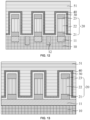
FIG. 12 is a schematic diagram of a first cross section after a first initial support layer is formed according to an embodiment of the present application; -
FIG. 13 is a schematic diagram of a second cross section after the first initial support layer is formed according to an embodiment of the present application; -
FIG. 14 is a schematic diagram of a first cross section after a first support layer is formed according to an embodiment of the present application; -
FIG. 15 is a schematic diagram of a second cross section after the first support layer is formed according to an embodiment of the present application; -
FIG. 16 is a schematic diagram of a first cross section after an initial WL layer is formed according to an embodiment of the present application; -
FIG. 17 is a schematic diagram of a second cross section after the initial WL layer is formed according to an embodiment of the present application; -
FIG. 18 is a schematic diagram of a first cross section after a first photoresist layer is formed according to an embodiment of the present application; -
FIG. 19 is a schematic diagram of a second cross section after the first photoresist layer is formed according to an embodiment of the present application; -
FIG. 20 is a schematic diagram of a first cross section after a mask layer is etched according to an embodiment of the present application; -
FIG. 21 is a schematic diagram of a second cross section after the mask layer is etched according to an embodiment of the present application; -
FIG. 22 is a schematic diagram of a first cross section after intermediate WL layers are formed according to an embodiment of the present application; -
FIG. 23 is a schematic diagram of a second cross section after the intermediate WL layers are formed according to an embodiment of the present application; -
FIG. 24 is a schematic diagram of a first cross section after a second photoresist layer is formed according to an embodiment of the present application; -
FIG. 25 is a schematic diagram of a second cross section after the second photoresist layer is formed according to an embodiment of the present application; -
FIG. 26 is a schematic diagram of a first cross section after a contact hole is formed according to an embodiment of the present application; -
FIG. 27 is a schematic diagram of a second cross section after the contact hole is formed according to an embodiment of the present application; -
FIG. 28 is a schematic diagram of a first cross section after the second photoresist layer is removed according to an embodiment of the present application; -
FIG. 29 is a schematic diagram of a second cross section after the second photoresist layer is removed according to an embodiment of the present application; -
FIG. 30 is another schematic diagram of the first cross section after the contact hole is formed according to an embodiment of the present application; -
FIG. 31 is another schematic diagram of the second cross section after the contact hole is formed according to an embodiment of the present application; -
FIG. 32 is a schematic diagram of a first cross section after a third conductive layer is formed according to an embodiment of the present application; and -
FIG. 33 is a schematic diagram of a second cross section after the third conductive layer is formed according to an embodiment of the present application. - In the manufacturing method of the semiconductor structure provided in embodiments of the present application, vertical transistors are formed, and at least one of a source and a drain in the vertical transistor is a semi-metal layer, to reduce a contact resistance between the vertical transistor and another structure, and a contact resistance inside the vertical transistor, thereby improving the performance of the semiconductor structure.
- In order to make the objectives, features and advantages of the embodiments of the present application clearer, the technical solutions in the embodiments of the present application are described clearly and completely below with reference to the accompanying drawings in the embodiments of the present application. Apparently, the described embodiments are some rather than all of the embodiments of the present application. All other embodiments obtained by those of ordinary skill in the art based on the embodiments of present application without creative efforts should fall within the protection scope of the present application.
- With reference to
FIG. 1 , an embodiment of the present application provides a manufacturing method of a semiconductor structure, including the following steps:
step S101: Provide a substrate. - A
substrate 10 may be a semiconductor substrate. For example, thesubstrate 10 may be a silicon substrate, a germanium substrate, a silicon germanium substrate, a gallium nitride substrate, a gallium arsenide substrate, a silicon-on-insulator (SOI) substrate, a germanium-on-insulator (GOI) substrate, or the like. Thesubstrate 10 may be doped or not. For example, thesubstrate 10 may be a N-type substrate or a P-type substrate. - In some possible examples, with reference to
FIG. 2 andFIG. 3 , a first cross section shown inFIG. 2 is a plane perpendicular to a second direction. A second cross section shown inFIG. 3 is a plane perpendicular to the second direction. A plurality ofBLs 11 may be also disposed in thesubstrate 10, are spaced apart from each other, and extend along the second direction. As shown inFIG. 3 , the plurality ofBLs 11 extend along a horizontal direction (a direction X shown inFIG. 3 ). As shown inFIG. 2 andFIG. 3 , theBLs 11 may be exposed on the surface of thesubstrate 10. TheBLs 11 are exposed on the upper surface of thesubstrate 10, to be electrically connected to another structure on thesubstrate 10. - With reference to
FIG. 2 andFIG. 3 , a shallow trench isolation (STI)structure 12 is also disposed in thesubstrate 10. TheSTI structure 12 is disposed between adjacent BLs 11, to isolate them. TheSTI structure 12 may be filled with an insulating material such as silicon nitride or silicon oxide. - Step S102: Form a plurality of laminated structures arranged at intervals on the substrate, where each of the laminated structures includes a first conductive layer, an insulating layer, and a second conductive layer that are stacked sequentially, and at least one of the first conductive layer and the second conductive layer is a semi-metal layer.
- With reference to
FIG. 4 and FIG. 5 , a plurality oflaminated structures 20 are formed on thesubstrate 10, and are disposed at intervals. Thelaminated structure 20 includes a firstconductive layer 21, an insulatinglayer 22, and a secondconductive layer 23. One of the firstconductive layer 21 and the secondconductive layer 23 is electrically connected to a capacitor, and the other of the firstconductive layer 21 and the secondconductive layer 23 is electrically connected to theBLs 11. For example, the firstconductive layer 21, the insulatinglayer 22, and the secondconductive layer 23 are stacked sequentially in a vertical direction (a direction Z shown inFIG. 5 ). The firstconductive layer 21 is electrically connected toBL 11, and the secondconductive layer 23 is electrically connected to the capacitor. - The insulating
layer 22 may be an oxide layer. For example, a material of the insulatinglayer 22 may be silicon oxide. At least one of the firstconductive layer 21 and the secondconductive layer 23 is a semi-metal layer. For example, the firstconductive layer 21 is a semi-metal layer, and the secondconductive layer 23 is also a semi-metal layer. A material of the semi-metal layer may be bismuth. The firstconductive layer 21 and/or the secondconductive layer 23 are/is disposed as a semi-metal layer, which can reduce a contact resistance between thelaminated structure 20 and theBL 11 and/or a capacitor, thereby improving the performance of the semiconductor structure. - With reference to
FIG. 4 and FIG. 5 , at least one oflaminated structures 20 is disposed on each of theBLs 11 along a second direction (a direction X shown inFIG. 5 ). The firstconductive layer 21 is in contact with theBL 11, such that the firstconductive layer 21 is electrically connected to theBL 11. Thelaminated structure 20 may be in a shape of a column, such as a cylinder, an elliptical column, a square column, or a rectangular column. Thelaminated structures 20 may be arranged in an array. - With reference to
FIG. 2 to FIG. 5 , in some possible examples, a plurality oflaminated structures 20 are arranged at intervals on thesubstrate 10, where thelaminated structure 20 includes the firstconductive layer 21, the insulatinglayer 22, and the secondconductive layer 23 that are stacked sequentially, and at least one of the firstconductive layer 21 and the secondconductive layer 23 is a semi-metal layer, which includes following steps. - The first
conductive layer 21, the insulatinglayer 22, and the secondconductive layer 23 that are stacked are formed through deposition on thesubstrate 10. As shown inFIG. 2 andFIG. 3 , the firstconductive layer 21 is deposited on thesubstrate 10, the insulatinglayer 22 is deposited on the firstconductive layer 21, and the secondconductive layer 23 is deposited on the insulatinglayer 22. The deposition may be a chemical vapor deposition (CVD), a physical vapor deposition (PVD), or an atomic layer deposition (ALD). - Then, the first
conductive layer 21, the insulatinglayer 22, and the secondconductive layer 23 are etched, to form the plurality oflaminated structures 20 arranged at intervals. As shown inFIG. 4 and FIG. 5 , a part of the firstconductive layer 21, a part of the insulatinglayer 22, and a part of the secondconductive layer 23 are removed through dry etching or wet etching, such that the retained firstconductive layer 21, the retained insulatinglayer 22, the retained secondconductive layer 23 are separated to form the plurality oflaminated structures 20 that are spaced apart from each other. - Step S103: Form a channel layer covering the laminated structures, and a dielectric layer covering the channel layer.
- With reference to
FIG. 6 to FIG. 9 , thechannel layer 30 covers thelaminated structures 20. Thedielectric layer 40 covers thechannel layer 30. Specifically, thechannel layer 30 covers the side surfaces and the top surfaces of thelaminated structures 20. Thedielectric layer 40 covers the side surface and the top surface of thechannel layer 30, where the top surface is away from thesubstrate 10. As shown inFIG. 6 and FIG. 7 , thechannel layer 30 covers an outer peripheral surface of the firstconductive layer 21, an outer peripheral surface of the insulatinglayer 22, and an outer peripheral surface of the secondconductive layer 23. Thechannel layer 30 further covers thetop surface 24 of the second conductive layer. - One of the first
conductive layer 21 and the secondconductive layer 23 forms a source, and the other forms a drain. Thechannel layer 30 surrounding the side surface of thelaminated structure 20 forms a channel region, to provide a conductive channel between the source and the drain, such that carriers can move from the source to the drain or vice versa. Thedielectric layer 40 may be an oxide layer, and thedielectric layer 40 on the side surface of thechannel layer 30 forms a gate oxide layer. - As shown in
FIG. 6 and FIG. 7 , the channel region is layered. A material of thechannel layer 30 may include molybdenum sulfide, such as molybdenum disulfide, transition metal sulfur compounds (TMDs), or the like. There is a band gap in the layered molybdenum sulfide, which forms a field effect transistor with a high on-off ratio. In addition, the layered molybdenum sulfide has a high specific surface area, which is beneficial to overcome the short channel effect. The on-off ratio refers to the ratio of the on-state current to the off-state current of a device. Specifically, in a transistor, when the source-drain voltage remains unchanged, the ratio of the source-drain current measured when the gate voltage is applied to that when the gate voltage is not applied is the on-off ratio. - In some possible embodiments, the material of the
channel layer 30 is molybdenum sulfide, and the material of the semi-metal layer is bismuth. Preferably, thechannel layer 30 is made of molybdenum sulfide, and the firstconductive layer 21 and the secondconductive layer 23 are both made of bismuth. Through such a disposal, the energy barriers at the interfaces of molybdenum sulfide and bismuth are reduced, which can reduce the metal-induced gap states (MIGSs) between thechannel layer 30 and the firstconductive layer 21, and between thechannel layer 30 and the secondconductive layer 23, thereby reducing the contact resistances between thechannel layer 30 and the firstconductive layer 21 and between thechannel layer 30 and the secondconductive layer 23. - In the embodiments of the present application, the
channel layer 30 covering thelaminated structures 20 and thedielectric layer 40 covering thechannel layer 30 are formed in the following steps:
Thechannel layer 30 is deposited on thelaminated structure 20 and thesubstrate 10, and thechannel layer 30 covers the top surfaces and the side surfaces of thelaminated structures 20, and the top surface of thesubstrate 10. With reference toFIG. 6 and FIG. 7 , thechannel layer 30 is formed through a deposition process. Thechannel layer 30 covers the top surfaces and the side surfaces of thelaminated structures 20, and the top surface of thesubstrate 10. Then, thedielectric layer 40 is deposited on thechannel layer 30. With reference toFIG. 8 and FIG. 9 , thedielectric layer 40 is formed through a deposition process. Thedielectric layer 40 covers the entire surface of thechannel layer 30. - Step S104: Form WLs extending along a first direction, where the WL includes a plurality of contact parts and a connecting part connecting adjacent contact parts, the contact part surrounds and is in contact with a side surface of the dielectric layer, and the contact part is opposite to at least a part of the insulating layer.
- With reference to
FIG. 10 and FIG. 11 , a plurality ofWLs 63 are formed between thelaminated structures 20 after thechannel layer 30 and thedielectric layer 40 are formed, are disposed at intervals, and extend along a first direction (a direction Y shown inFIG.10 ). As shown inFIG. 10 and FIG. 11 , theWL 63 includes a plurality ofcontact parts 64 and a connectingpart 65 connectingadjacent contact parts 64. Thecontact part 64 surrounds and is in contact with a side surface of thedielectric layer 40. - As shown in
FIG. 10 and FIG. 11 , thecontact part 64 corresponds to a part of the insulatinglayer 22. Thecontact part 64 serves as a gate of the transistor, that is, a part of theWL 63 serves as a gate. In a direction (a direction Z shown inFIG. 10 ) perpendicular to thesubstrate 10, the orthographic projection of the insulatinglayer 22 partially overlaps with that of thecontact part 64. For example, the top surface of thecontact part 64 is lower than that of the insulatinglayer 22, and a bottom of thecontact part 64 is higher than that of the insulatinglayer 22. - Along a first direction, the connecting
part 65 connects twoadjacent contact parts 64. The heights of the connectingpart 65 and thecontact part 64 may be same or not. The specific structure of the connectingpart 65 may be determined according to a specific condition. - Above all, in the embodiments of the present application, the first
conductive layer 21, the insulatinglayer 22, and the secondconductive layer 23 are stacked sequentially to form thelaminated structure 20. At least one of the firstconductive layer 21 and the secondconductive layer 23 is a semi-metal layer, which can not only reduce a contact resistance between alaminated structure 20 and another structure, but a contact resistance between the firstconductive layer 21 and/or the secondconductive layer 23 and thechannel layer 30, thereby improving the performance of the semiconductor structure. In addition, the firstconductive layer 21, the insulatinglayer 22, the secondconductive layer 23, thechannel layer 30, thedielectric layer 40, and thecontact part 64 form a vertical transistor. Adjusting the height of thelaminated structure 20 can increase the height of thechannel layer 30, which facilitates improving the short-channel effects of the transistor, thereby improving the performance of the semiconductor structure. - In a possible embodiment of the present application, with reference to
FIG. 12 to FIG. 15 , before the WLs 63 extending along the first direction are formed, where theWL 63 includes the plurality ofcontact parts 64 and the connectingpart 65 connectingadjacent contact parts 64, thecontact part 64 surrounds and is in contact with the side surface of thedielectric layer 40, and thecontact part 64 is opposite to at least a part of the insulatinglayer 22, the manufacturing method further includes: filling afirst support layer 50 between thelaminated structures 20 covered by thechannel layer 30 and thedielectric layer 40, where a surface of thefirst support layer 50 away from thesubstrate 10 is higher than that of the firstconductive layer 21 away fromsubstrate 10, and is lower than a surface of the insulatinglayer 22 away from thesubstrate 10. - As shown in
FIG. 12 to FIG. 15 , thefirst support layer 50 may be used as a cushion layer to increase the pitch between theWL 63 formed subsequently and thesubstrate 10, such that the bottom surface of theWL 63 is higher than the top surface of the firstconductive layer 21, that is, the surface of theWL 63 facing thesubstrate 10 is higher than the surface of the firstconductive layer 21 away from thesubstrate 10. In this case, the surface of thefirst support layer 50 away from thesubstrate 10 is lower than the surface of the insulatinglayer 22 away from thesubstrate 10, such that the bottom surface of theWL 63 is lower than the top surface of the firstconductive layer 21, thereby ensuring that theWL 63 is opposite to the insulatinglayer 22. The material of thefirst support layer 50 may be silicon nitride or silicon oxynitride, and thefirst support layer 50 and thedielectric layer 40 have a relatively large selectivity. For example, the selectivity of thefirst support layer 50 to thedielectric layer 40 is greater than 5, to avoid damaging thedielectric layer 40 when thefirst support layer 50 is etched, thereby reducing damage on the gate oxide layer in the transistor. - In a possible implementation of the present application, with reference to
FIG. 12 to FIG. 15 , the filling afirst support layer 50 between thelaminated structures 20 covered by thechannel layer 30 and thedielectric layer 40, where a surface of thefirst support layer 50 away from thesubstrate 10 is higher than that of the firstconductive layer 21 away from thesubstrate 10, and is lower than a surface of the insulatinglayer 22 away from thesubstrate 10 may include the following process:
A firstinitial support layer 51 is formed on thedielectric layer 40, where the firstinitial support layer 51 is filled between thelaminated structures 20 covered by thechannel layer 30 and thedielectric layer 40, and the firstinitial support layer 51 covers a top surface of thedielectric layer 40. As shown inFIG. 12 and FIG. 13 , the firstinitial support layer 51 is formed through deposition and is filled between thelaminated structures 20 covered by thechannel layer 30 and thedielectric layer 40. The firstinitial support layer 51 further covers the top surface of thedielectric layer 40. Specifically, the upper surface of the firstinitial support layer 51 is higher than the upper surface of thedielectric layer 40. - After the first
initial support layer 51 is formed, a part of the firstinitial support layer 51 is removed, and the retained firstinitial support layer 51 forms thefirst support layer 50. As shown inFIG. 14 and FIG. 15 , along a direction perpendicular to thesubstrate 10, a part of the firstinitial support layer 51 is removed through dry etching or wet etching. The part of the firstinitial support layer 51 located between thelaminated structures 20 covered by thechannel layer 30 and thedielectric layer 40 is retained. The retained firstinitial support layer 51 forms thefirst support layer 50. - Based on the foregoing embodiments, after the
first support layer 50 is formed, in a possible embodiment, with reference toFIG. 16 to FIG. 23 , theWLs 63 extending along the first direction are formed, where theWL 63 includes the plurality ofcontact parts 64 and the connectingpart 65 connectingadjacent contact parts 64, thecontact part 64 surrounds and is in contact with the side surface of thedielectric layer 40, and thecontact part 64 is opposite to at least a part of the insulatinglayer 22, which may include the following steps:
Step S1041: Form an initial WL layer covering the first support layer and the dielectric layer. - With reference to
FIG. 16 andFIG. 17 , the initial WL layer 61 is formed through a deposition process, and covers thefirst support layer 50 and thedielectric layer 40. As shown inFIG. 16 andFIG. 17 , the initial WL layer 61 covers the top surface of thefirst support layer 50, and covers the side surface and the top surface of thedielectric layer 40. There is also a gap in the initial WL layer 61 covering the side surfaces of thedielectric layer 40, that is, the initial WL layer 61 is not filled between thelaminated structures 20 covered by thechannel layer 30 and thedielectric layer 40. - Step S1042: Remove a part of the initial WL layer located on the first support layer along the first direction, such that the initial WL layer is divided, to form a plurality of intermediate WL layers arranged at intervals.
- With reference to
FIG. 18 to FIG. 23 , the part of the initial WL layer 61 located on thefirst support layer 50 is removed, such that the initial WL layer 61 is divided, to form the plurality of intermediate WL layers 62 arranged at intervals. The intermediate WL layers 62 extend along the first direction, that is, a part of the initial WL layer 61 on thefirst support layer 50 is removed along the first direction, the retained initial WL layer 61 forms the intermediate WL layers 62. - Specifically, as shown in
FIG. 18 to FIG. 23 , the part of the initial WL layer 61 located on thefirst support layer 50 is removed along the first direction, such that the initial WL layer 61 forms the plurality of intermediate WL layers 62 arranged at intervals, which may further include the following process:
Amask layer 71 covering the initial WL layer 61 is formed and is filled between thelaminated structures 20 covered by thechannel layer 30, thedielectric layer 40, and the initial WL layer 61. Themask layer 71 covers the top surface of the initial WL layer 61. As shown inFIG. 18 andFIG. 19 , themask layer 71 is deposited on the initial WL layer 61. Themask layer 71 is filled between thelaminated structures 20 covered by thechannel layer 30, thedielectric layer 40, and the initial WL layer 61. Themask layer 71 further covers the top surface of the initial WL layer 61. The top surface of themask layer 71 is higher than the top surface of the initial WL layer 61. - After the
mask layer 71 is formed, afirst photoresist layer 72 is formed thereon. Thefirst photoresist layer 72 is provided with atrench 73 extending along the first direction, and orthographic projection of thetrench 73 on thesubstrate 10 and that of the initial WL layer 61 on the side surface of thelaminated structure 20 on thesubstrate 10 do not overlap. As shown inFIG. 18 andFIG. 19 , thefirst photoresist layer 72 is spin-coated on themask layer 71. Thefirst photoresist layer 72 is provided with atrench 73 running through thefirst photoresist layer 72. Thetrench 73 is staggered from the initial WL layer 61 on the side surface and the top surface of thedielectric layer 40, and is opposite to a part of the initial WL layer 61 on thefirst support layer 50. - After the
first photoresist layer 72 is formed, themask layer 71 is etched by using thefirst photoresist layer 72 as a mask. Themask layer 71 is etched by using thefirst photoresist layer 72 as a mask. The pattern on thefirst photoresist layer 72 is transferred to themask layer 71. As shown inFIG. 20 andFIG. 21 , the initial WL layer 61 is exposed from the pattern formed by themask layer 71. - After the
mask layer 71 is etched, the initial WL layer 61 is etched by using the etchedmask layer 71 as a mask, to form the intermediate WL layers 62. A part of the initial WL layer 61 on thefirst support layer 50 is removed through anisotropic etching. As shown inFIG. 22 and FIG. 23 , the retained initial WL layer 61 forms intermediate WL layers 62. Gaps between a plurality of intermediate WL layers 62 expose thefirst support layer 50. - Step S1043: Remove the intermediate WL layer on a top surface of the dielectric layer, and a part of the intermediate WL layer away from the substrate on the side surface of the dielectric layer, and taking the retained intermediate WL layers as the WLs.
- The
intermediate WL layer 62 on a top surface of thedielectric layer 40 and a part of theintermediate WL layer 62 on the side surface of thedielectric layer 40 are removed through etching. The retained intermediate WL layers 62 form theWLs 63. As shown inFIG. 10 and FIG. 11 , the top surface of theWL 63 is lower than the top surface of the insulatinglayer 22, and theWL 63 is opposite to the insulatinglayer 22. - In another possible embodiment of the present application, after the
WLs 63 extending along the first direction are formed, where theWL 63 includes the plurality ofcontact parts 64 and the connectingpart 65 connectingadjacent contact parts 64, thecontact part 64 is connected to thelaminated structure 20, and thecontact part 64 surrounds the side surface of thedielectric layer 40, with reference toFIG. 24 to FIG. 33 , the manufacturing method of the semiconductor structure further includes:
forming asecond support layer 81 covering theWLs 63, thefirst support layer 50, and thesecond support layer 50 on thedielectric layer 40. As shown inFIG. 24 and FIG. 25 , thesecond support layer 81 is deposited. Thesecond support layer 81 covers theWLs 63, thefirst support layer 50, and thedielectric layer 40. The top surface of thesecond support layer 81 is higher than the top surface of thedielectric layer 40. The surface of thesecond support layer 81 away from thesubstrate 10 may be flat. For example, thesecond support layer 81 is flattened, through, for example, chemical mechanical polishing (CMP), to make the top surface of thesecond support layer 81 flat. Thesecond support layer 81 and thefirst support layer 50 may be made of a same insulating material, such that thesecond support layer 81 is integrated with thefirst support layer 50. Thesecond support layer 81 and thefirst support layer 50 cover and isolate the WLs 63 to insulate theWLs 63. - After the
second support layer 81 is formed, thesecond photoresist layer 82 is formed on thesecond support layer 81. Thesecond photoresist layer 82 is provided with a plurality ofopenings 83. Theopenings 83 are opposite to thelaminated structures 20. As shown inFIG. 24 and FIG. 25 , thesecond photoresist layer 82 is formed on thesecond support layer 81. Thesecond photoresist layer 82 is provided with a plurality ofopenings 83. The plurality ofopenings 83 correspond to the plurality oflaminated structures 20 respectively, and theopening 83 is opposite to thelaminated structure 20 corresponding thereto. Orthographic projection of theopening 83 on thesubstrate 10 is located within that of thelaminated structure 20 corresponding thereto on thesubstrate 10, or the orthographic projection of theopening 83 on thesubstrate 10 overlaps with that of thelaminated structure 20 corresponding thereto on thesubstrate 10. - After the
second photoresist layer 82 is formed, thesecond support layer 81, thedielectric layer 40, and thechannel layer 30 are etched by using thesecond photoresist layer 82 as a mask, to form thecontact hole 84. Thecontact hole 84 exposes the secondconductive layer 23. As shown inFIG. 26 and FIG. 27 , thecontact hole 84 runs through thesecond support layer 81, thedielectric layer 40, and thechannel layer 30, to expose the secondconductive layer 23. Thesecond photoresist layer 82 is removed while thecontact hole 84 is formed, or thesecond photoresist layer 82 is removed after thecontact hole 84 is formed. As shown inFIG. 28 and FIG. 29 , after thesecond photoresist layer 82 is removed, the top surface of thesecond support layer 81 is exposed. - It should be noted that an area of an
opening 83 at thecontact hole 84 is greater than that of a bottom of thecontact hole 84, that is, a width of an upper part of thecontact hole 84 is relatively large while a width of its lower part is relatively small. Through such a disposal, after the thirdconductive layer 90 is formed in thecontact hole 84, a width of an upper part of the thirdconductive layer 90 is relatively large. Adding the width of the operation window facilitates the alignment with the capacitor. In addition, the width of the lower part of the thirdconductive layer 90 is relatively small, which can reduce the critical dimension of the transistor. - For example, a plane perpendicular to the
substrate 10 is used as a cross section. A shape of a cross section of thecontact hole 84 may be an inverted trapezoid with a large top and a small bottom. As shown inFIG. 30 and FIG. 31 , the shape of the cross section of thecontact hole 84 may be also a rectangle and a trapezoid that are connected to each other. The rectangle is disposed at one side of the trapezoid close to thesubstrate 10, and a bottom edge of the rectangle coincides with an upper bottom of the trapezoid. - After the
contact hole 84 is formed, the thirdconductive layer 90 is formed in thecontact hole 84, and the thirdconductive layer 90 is electrically connected to the second conductive layer. As shown inFIG. 32 and FIG. 33 , the thirdconductive layer 90 is deposited in thecontact hole 84, and the thirdconductive layer 90 is in contact with the secondconductive layer 23, such that the thirdconductive layer 90 is electrically connected to the secondconductive layer 23. The thirdconductive layer 90 may be a capacitive contact pad, and a capacitor is formed on the thirdconductive layer 90. - With reference to
FIG. 10 and FIG. 11 , an embodiment of the present application further provides a semiconductor structure, including: laminatedstructures 20, achannel layer 30, adielectric layer 40, and a gate. Thelaminated structures 20 are disposed on thesubstrate 10. Thesubstrate 10 is configured to support thelaminated structures 20. Thesubstrate 10 may be a semiconductor substrate such as a silicon substrate. - A plurality of
BLs 11 may be also disposed in thesubstrate 10, are spaced apart from each other, and extend along the second direction (the direction X shown inFIG. 11 ). TheBLs 11 may be exposed on the surface of thesubstrate 10, to be electrically connected to another structure on thesubstrate 10. AnSTI structure 12 may also be disposed between adjacent BLs 11, which are isolated by theSTI structure structures 12. - The plurality of
laminated structures 20 are formed on thesubstrate 10, and are disposed at intervals. Thelaminated structure 20 includes a firstconductive layer 21, an insulatinglayer 22, and a secondconductive layer 23 that are stacked. As shown inFIG. 10 and FIG. 11 , along the direction away from thesubstrate 10, the firstconductive layer 21, the insulatinglayer 22, and the secondconductive layer 23 are disposed sequentially. One of the firstconductive layer 21 and the secondconductive layer 23 is a source, the other of the firstconductive layer 21 and the secondconductive layer 23 is a drain. At least one of the source and the drain is a semi-metal layer. The material of the semi-metal layer may be bismuth, and the material of the insulatinglayer 22 may be silicon oxide. Disposing at least one of the source or the drain as a semi-metal layer can reduce the contact resistance between thelaminated structure 20 and another structure (for example, theBL 11 and/or the capacitor), thereby improving the performance of the semiconductor structure. - With reference to
FIG. 10 and FIG. 11 , along the second direction, at least one of thelaminated structures 20 is disposed on each of theBLs 11, and one of the source and the drain in thelaminated structure 20 is in contact with theBL 11, such that the source or drain is electrically connected to theBL 11. Thelaminated structure 20 may be in a shape of a column, such as a cylinder, an elliptical column, a square column, or a rectangular column. Thelaminated structures 20 may be arranged in an array. - The
channel layer 30 covers the side surface of thelaminated structure 20. Thechannel layer 30 surrounding the side surface of thelaminated structure 20 forms a channel region, to provide a conductive channel between the source and the drain, such that carriers can move from the source to the drain or vice versa. The channel region is layered. A material of thechannel layer 30 may include molybdenum sulfide, such as molybdenum disulfide. There is a band gap in the layered molybdenum sulfide, which forms a field effect transistor with a high on-off ratio. Preferably, the material of thechannel layer 30 is molybdenum sulfide, and the materials of the source and the drain are both bismuth, to reduce the MIGSs and energy barriers between thechannel layer 30 and the source, and between thechannel layer 30 and the drain, thereby reducing the contact resistances between thechannel layer 30 and the source and between thechannel layer 30 and the drain. - The
dielectric layer 40 covers the side surface of thechannel layer 30 and may be an oxide layer. Thedielectric layer 40 located on the side surface of thechannel layer 30 forms a gate oxide layer. For example, thedielectric layer 40 is made of silicon oxide. - Withe reference to
FIG. 10 and FIG. 11 , a gate is annularly provided on thedielectric layer 40. The gate surrounds and is in contact with the side surface of thedielectric layer 40. The gate is opposite to at least a part of the insulatinglayer 22. Along a direction (the direction Z shown inFIG. 10 ) perpendicular to thesubstrate 10, the orthographic projection of thedielectric layer 40 at least partially overlaps with that of the gate. For example, the top surface of the gate is lower than the top surface of thedielectric layer 40, and the bottom surface of the gate is higher than the bottom surface of thedielectric layer 40. - The semiconductor structure in the embodiments of the present application further includes
WLs 63. TheWLs 63 extend along the first direction. TheWL 63 includescontact parts 64 and a connectingpart 65 connecting twoadjacent contact parts 64. Thecontact part 64 is a gate disposed annularly on thedielectric layer 40, that is, a part of theWL 63 is a gate. It can be understood that, along the first direction, the connectingpart 65 and the gate are arranged at intervals, and the connectingpart 65 connects the plurality of gates in the first direction into one to form theWLs 63. - In some possible examples, with reference to
FIG. 32 and FIG. 33 , theWL 63 is disposed on thefirst support layer 50. Thefirst support layer 50 is located below theWL 63 and is filled betweenlaminated structures 20 covered by thedielectric layer 40 and thechannel layer 30, to elevate theWLs 63. Thesecond support layer 81 may further cover theWLs 63, and thesecond support layer 81 and thefirst support layer 50 electrically isolate theWLs 63. Thesecond support layer 81 and thefirst support layer 50 may be made of a same material, such that thesecond support layer 81 is integrated with thefirst support layer 50. - With reference to
FIG. 32 and FIG. 33 , thesecond support layer 81 also covers thedielectric layer 40. Thesecond support layer 81 is provided with a contact hole running through thedielectric layer 40 and thechannel layer 30, to expose the secondconductive layer 23 in thelaminated structures 20. The thirdconductive layer 90 fills the contact hole, and one end of the thirdconductive layer 90 is in contact with the secondconductive layer 23, such that the thirdconductive layer 90 is electrically connected to the secondconductive layer 23. The other end of the thirdconductive layer 90 may be connected to a capacitor. - In the semiconductor structure provided by the embodiments of the present application, the first
conductive layer 21, the insulatinglayer 22, and the secondconductive layer 23 are stacked sequentially to form thelaminated structure 20. One of the firstconductive layer 21 and the secondconductive layer 23 is the source and the other is the drain. At least one of the firstconductive layer 21 and the secondconductive layer 23 is a semi-metal layer, which can not only reduce a contact resistance between alaminated structure 20 and another structure, but a contact resistance between the firstconductive layer 21 and/or the secondconductive layer 23 and thechannel layer 30, thereby improving the performance of the semiconductor structure. In addition, thechannel layer 30 covers the side surface of thelaminated structure 20. Thedielectric layer 40 covers the side surface of thechannel layer 30. A gate is annularly provided on thedielectric layer 40. Thelaminated structures 20, thechannel layer 30, thedielectric layer 40, and the gate form a vertical transistor. Adjusting the height of thelaminated structure 20 can increase the height of thechannel layer 30, which facilitates improving the short-channel effects of the transistor, thereby improving the performance of the semiconductor structure. - The embodiments or implementations of this specification are described in a progressive manner, and each embodiment focuses on differences from other embodiments. The same or similar parts between the embodiments may refer to each other.
- In the descriptions of this specification, a description with reference to the term "one implementation", "some implementations", "an exemplary implementation", "an example", "a specific example", "some examples", or the like means that a specific feature, structure, material, or characteristic described in combination with the implementation(s) or example(s) is included in at least one implementation or example of the present application. In this specification, the schematic expression of the above terms does not necessarily refer to the same embodiment or example. Moreover, the described specific feature, structure, material or characteristic may be combined in an appropriate manner in any one or more implementations or examples.
- Finally, it should be noted that the above embodiments are merely used to explain the technical solutions of the present application, but are not intended to limit the present application. Although the present application is described in detail with reference to the foregoing embodiments, those of ordinary skill in the art should understand that they can still modify the technical solutions described in the foregoing embodiments, or make equivalent substitutions on some or all technical features therein. These modifications or substitutions do not make the essence of the corresponding technical solutions deviate from the spirit and scope of the technical solutions of the embodiments of the present application.
Claims (15)
- A manufacturing method of a semiconductor structure, comprising:providing a substrate;forming a plurality of laminated structures arranged at intervals on the substrate, wherein each of the laminated structures comprises a first conductive layer, an insulating layer, and a second conductive layer that are stacked sequentially, and at least one of the first conductive layer and the second conductive layer is a semi-metal layer;forming a channel layer covering the laminated structures, and a dielectric layer covering the channel layer; andforming word lines (WLs) extending along a first direction, wherein the WL comprises a plurality of contact parts and a connecting part connecting adjacent contact parts, the contact part surrounds and is in contact with a side surface of the dielectric layer, and the contact part is opposite to at least a part of the insulating layer.
- The manufacturing method of a semiconductor structure according to claim 1, wherein a material of the channel layer comprises molybdenum sulfide, and/or a material of the semi-metal layer comprises bismuth.
- The manufacturing method of a semiconductor structure according to claim 1, wherein the forming a channel layer covering the laminated structures, and a dielectric layer covering the channel layer comprises:depositing the channel layer on the laminated structures and the substrate, wherein the channel layer covers top surfaces and side surfaces of the laminated structures, and a top surface of the substrate; anddepositing the dielectric layer on the channel layer.
- The manufacturing method of a semiconductor structure according to claim 3, before the forming WLs extending along a first direction, wherein the WL comprises a plurality of contact parts and a connecting part connecting adjacent contact parts, the contact part surrounds and is in contact with a side surface of the dielectric layer, and the contact part is opposite to at least a part of the insulating layer, the manufacturing method further comprises:
filling a first support layer between the laminated structures covered by the channel layer and the dielectric layer, wherein a surface of the first support layer away from the substrate is higher than that of the first conductive layer away from the substrate, and is lower than a surface of the insulating layer away from the substrate. - The manufacturing method of a semiconductor structure according to claim 4, wherein the filling a first support layer between the laminated structures covered by the channel layer and the dielectric layer, wherein a surface of the first support layer away from the substrate is higher than that of the first conductive layer away from the substrate, and is lower than a surface of the insulating layer away from the substrate comprises:forming a first initial support layer on the dielectric layer, wherein the first initial support layer is filled between the laminated structures covered by the channel layer and the dielectric layer, and the first initial support layer covers a top surface of the dielectric layer; andremoving a part of the first initial support layer, and taking the retained first initial support layer as the first support layer.
- The manufacturing method of a semiconductor structure according to claim 4, wherein the forming WLs extending along a first direction, wherein the WL comprises a plurality of contact parts and a connecting part connecting adjacent contact parts, the contact part surrounds and is in contact with a side surface of the dielectric layer, and the contact part is opposite to at least a part of the insulating layer comprises:forming an initial WL layer covering the first support layer and the dielectric layer;removing a part of the initial WL layer located on the first support layer along the first direction, such that the initial WL layer is divided, to form a plurality of intermediate WL layers arranged at intervals; andremoving the intermediate WL layer on a top surface of the dielectric layer, and a part of the intermediate WL layer away from the substrate on the side surface of the dielectric layer, and taking the retained intermediate WL layers as the WLs.
- The manufacturing method of a semiconductor structure according to claim 6, wherein the removing a part of the initial WL layer located on the first support layer along the first direction, such that the initial WL layer is divided, to form a plurality of intermediate WL layers arranged at intervals comprises:forming a mask layer covering the initial WL layer, wherein the mask layer is filled between the laminated structures covered by the channel layer, the dielectric layer, and the initial WL layer, and the mask layer covers a top surface of the initial WL layer;forming a first photoresist layer on the mask layer, wherein the first photoresist layer is provided with a trench extending along the first direction, and orthographic projection of the trench on the substrate and that of the initial WL layer on the side surface of the laminated structure on the substrate do not overlap;etching the mask layer by the first photoresist layer as a mask; andetching the initial WL layer by the etched mask layer as a mask, to form the intermediate WL layers.
- The manufacturing method of a semiconductor structure according to claim 4, after the forming WLs extending along a first direction, wherein the WL comprises a plurality of contact parts and a connecting part connecting adjacent contact parts, the contact part surrounds and is in contact with a side surface of the dielectric layer, and the contact part is opposite to at least a part of the insulating layer, the manufacturing method further comprises:forming a second support layer covering the WLs, the first support layer, and the dielectric layer, wherein a surface of the second support layer away from the substrate is flat;forming a second photoresist layer on the second support layer, wherein the second photoresist layer is provided with a plurality of openings, and the openings are directly opposite to the laminated structures;etching the second support layer, the dielectric layer, and the channel layer by the second photoresist layer as a mask, to form a contact hole, wherein the contact hole exposes the second conductive layer; andforming a third conductive layer in the contact hole, wherein the third conductive layer is electrically connected to the second conductive layer.
- The manufacturing method of a semiconductor structure according to claim 8, wherein an area of an opening of the contact hole is greater than that of a bottom of the contact hole.
- The manufacturing method of a semiconductor structure according to claim 9, wherein a plane perpendicular to the substrate is used as a cross section, a shape of a cross section of the contact hole comprises a rectangle and a trapezoid that are connected to each other, the rectangle is disposed at one side of the trapezoid close to the substrate, and a bottom edge of the rectangle coincides with an upper bottom of the trapezoid.
- The manufacturing method of a semiconductor structure according to claim 1, wherein a plurality of bit lines (BLs) are arranged at intervals in the substrate, and the BLs extend along a second direction; and
at least one of the laminated structures is disposed on each of the BLs along the second direction, and the first conductive layer is electrically connected to the BLs. - The manufacturing method of a semiconductor structure according to claim 11, wherein a shallow trench isolation (STI) structure is also disposed in the substrate, and the STI structure is disposed between adjacent BLs.
- A semiconductor structure, comprising: laminated structures, a channel layer covering side surfaces of the laminated structures, and a dielectric layer covering a side surface of the channel layer, and a gate annularly provided on the dielectric layer; wherein
each of the laminated structures comprises a first conductive layer, an insulating layer, and a second conductive layer that are stacked sequentially, one of the first conductive layer and the second conductive layer is a source, the other of the first conductive layer and the second conductive layer is a drain, and at least one of the source and the drain is a semi-metal layer. - The semiconductor structure according to claim 13, wherein a material of the channel layer comprises molybdenum sulfide, and/or a material of the semi-metal layer comprises bismuth.
- The semiconductor structure according to claim 13, wherein the semiconductor structure further comprises WLs and BLs; and
the BLs are disposed in the substrate, the laminated structures are disposed on the substrate, one of the source and the drain is electrically connected to the BL, the WL comprises gates and a connecting part connecting two adjacent gates.
Applications Claiming Priority (2)
| Application Number | Priority Date | Filing Date | Title |
|---|---|---|---|
| CN202111231509.3A CN116033735A (en) | 2021-10-22 | 2021-10-22 | Semiconductor structure and manufacturing method thereof |
| PCT/CN2022/070590 WO2023065542A1 (en) | 2021-10-22 | 2022-01-06 | Semiconductor structure and fabrication method therefor |
Publications (2)
| Publication Number | Publication Date |
|---|---|
| EP4199085A1 true EP4199085A1 (en) | 2023-06-21 |
| EP4199085A4 EP4199085A4 (en) | 2024-05-01 |
Family
ID=84104937
Family Applications (1)
| Application Number | Title | Priority Date | Filing Date |
|---|---|---|---|
| EP22865907.4A Pending EP4199085A4 (en) | 2021-10-22 | 2022-01-06 | Semiconductor structure and fabrication method therefor |
Country Status (4)
| Country | Link |
|---|---|
| US (1) | US11508731B1 (en) |
| EP (1) | EP4199085A4 (en) |
| JP (1) | JP2023553023A (en) |
| KR (1) | KR20230096109A (en) |
Families Citing this family (1)
| Publication number | Priority date | Publication date | Assignee | Title |
|---|---|---|---|---|
| US10504999B2 (en) * | 2018-03-15 | 2019-12-10 | Taiwan Semiconductor Manufacturing Co., Ltd. | Forming semiconductor structures with semimetal features |
Family Cites Families (6)
| Publication number | Priority date | Publication date | Assignee | Title |
|---|---|---|---|---|
| US7205604B2 (en) * | 2001-03-13 | 2007-04-17 | International Business Machines Corporation | Ultra scalable high speed heterojunction vertical n-channel MISFETs and methods thereof |
| US7262096B2 (en) | 2004-01-15 | 2007-08-28 | Powerchip Semiconductor Corp. | NAND flash memory cell row and manufacturing method thereof |
| US9698261B2 (en) | 2014-06-30 | 2017-07-04 | Taiwan Semiconductor Manufacturing Co., Ltd. | Vertical device architecture |
| CN106328654B (en) | 2015-07-08 | 2019-03-26 | 上海复旦微电子集团股份有限公司 | Semiconductor devices and forming method thereof |
| DE102021108598A1 (en) | 2020-05-29 | 2021-12-02 | Taiwan Semiconductor Manufacturing Company, Ltd. | HETEROSTRUCTURAL OXIDE SEMICONDUCTOR TRANSISTOR WITH VERTICAL GATE-ALL-AROUND (VGAA) AND PROCESS FOR THE PRODUCTION OF IT |
| CN111969058B (en) | 2020-07-30 | 2022-07-01 | 电子科技大学中山学院 | Molybdenum disulfide field effect transistor and preparation method and application thereof |
-
2022
- 2022-01-06 KR KR1020237018619A patent/KR20230096109A/en not_active Application Discontinuation
- 2022-01-06 EP EP22865907.4A patent/EP4199085A4/en active Pending
- 2022-01-06 JP JP2023534229A patent/JP2023553023A/en active Pending
- 2022-06-20 US US17/807,747 patent/US11508731B1/en active Active
Also Published As
| Publication number | Publication date |
|---|---|
| KR20230096109A (en) | 2023-06-29 |
| JP2023553023A (en) | 2023-12-20 |
| EP4199085A4 (en) | 2024-05-01 |
| US11508731B1 (en) | 2022-11-22 |
Similar Documents
| Publication | Publication Date | Title |
|---|---|---|
| US10553582B2 (en) | Semiconductor device and method of manufacturing the same | |
| US7473611B2 (en) | Methods of forming non-volatile memory cells including fin structures | |
| WO2023130883A1 (en) | Semiconductor structure and method for manufacturing same | |
| KR20090017041A (en) | Nonvolatile memory device and method of fabricating the same | |
| US20100102361A1 (en) | Vertical transistor and fabricating method thereof and vertical transistor array | |
| CN112992775B (en) | Semiconductor memory and forming method thereof | |
| US20220085043A1 (en) | Semiconductor device, manufacturing method therefor, integrated circuit and electronic device | |
| US11670677B2 (en) | Crossing multi-stack nanosheet structure and method of manufacturing the same | |
| KR20130021661A (en) | Method of semiconductor device | |
| US20070004129A1 (en) | Semiconductor device having finfet and method of fabricating the same | |
| US11508731B1 (en) | Semiconductor structure and manufacturing method thereof | |
| US8878253B2 (en) | Semiconductor devices | |
| US20230016088A1 (en) | Semiconductor structure and fabrication method thereof | |
| WO2022041896A1 (en) | Semiconductor structure and manufacturing method therefor | |
| WO2014126214A1 (en) | Semiconductor device | |
| WO2022077940A1 (en) | Semiconductor device and manufacturing method therefor | |
| WO2023065542A1 (en) | Semiconductor structure and fabrication method therefor | |
| US11569232B2 (en) | Semiconductor device including self-aligned gate structure and method of manufacturing the same | |
| US20230135946A1 (en) | Self-Aligned Gate Contact Fin Field Effect Transistor and Method for Manufacturing the Same | |
| US11600709B2 (en) | Memory cell and fabricating method of the same | |
| US20230269933A1 (en) | Transistor structure and semiconductor device using the same | |
| EP4358672A1 (en) | Semiconductor structure and forming method therefor | |
| US20230422479A1 (en) | Semiconductor device | |
| US20230422477A1 (en) | Semiconductor structure and manufacturing method therefor | |
| US20230422466A1 (en) | Semiconductor structure and formation method thereof |
Legal Events
| Date | Code | Title | Description |
|---|---|---|---|
| STAA | Information on the status of an ep patent application or granted ep patent |
Free format text: STATUS: UNKNOWN |
|
| STAA | Information on the status of an ep patent application or granted ep patent |
Free format text: STATUS: THE INTERNATIONAL PUBLICATION HAS BEEN MADE |
|
| PUAI | Public reference made under article 153(3) epc to a published international application that has entered the european phase |
Free format text: ORIGINAL CODE: 0009012 |
|
| STAA | Information on the status of an ep patent application or granted ep patent |
Free format text: STATUS: REQUEST FOR EXAMINATION WAS MADE |
|
| 17P | Request for examination filed |
Effective date: 20230315 |
|
| AK | Designated contracting states |
Kind code of ref document: A1 Designated state(s): AL AT BE BG CH CY CZ DE DK EE ES FI FR GB GR HR HU IE IS IT LI LT LU LV MC MK MT NL NO PL PT RO RS SE SI SK SM TR |
|
| REG | Reference to a national code |
Ref country code: DE Ref legal event code: R079 Free format text: PREVIOUS MAIN CLASS: H01L0027100000 Ipc: H01L0029786000 |