EP4199042A1 - Memory device, and semiconductor structure and forming method therefor - Google Patents
Memory device, and semiconductor structure and forming method therefor Download PDFInfo
- Publication number
- EP4199042A1 EP4199042A1 EP21920574.7A EP21920574A EP4199042A1 EP 4199042 A1 EP4199042 A1 EP 4199042A1 EP 21920574 A EP21920574 A EP 21920574A EP 4199042 A1 EP4199042 A1 EP 4199042A1
- Authority
- EP
- European Patent Office
- Prior art keywords
- interface layer
- gate trench
- layer
- conductive material
- gate
- Prior art date
- Legal status (The legal status is an assumption and is not a legal conclusion. Google has not performed a legal analysis and makes no representation as to the accuracy of the status listed.)
- Pending
Links
Images





Classifications
-
- H—ELECTRICITY
- H10—SEMICONDUCTOR DEVICES; ELECTRIC SOLID-STATE DEVICES NOT OTHERWISE PROVIDED FOR
- H10D—INORGANIC ELECTRIC SEMICONDUCTOR DEVICES
- H10D64/00—Electrodes of devices having potential barriers
- H10D64/01—Manufacture or treatment
- H10D64/013—Manufacture or treatment of electrodes having a conductor capacitively coupled to a semiconductor by an insulator
-
- H—ELECTRICITY
- H10—SEMICONDUCTOR DEVICES; ELECTRIC SOLID-STATE DEVICES NOT OTHERWISE PROVIDED FOR
- H10B—ELECTRONIC MEMORY DEVICES
- H10B12/00—Dynamic random access memory [DRAM] devices
- H10B12/01—Manufacture or treatment
- H10B12/02—Manufacture or treatment for one transistor one-capacitor [1T-1C] memory cells
- H10B12/05—Making the transistor
- H10B12/053—Making the transistor the transistor being at least partially in a trench in the substrate
-
- G—PHYSICS
- G11—INFORMATION STORAGE
- G11C—STATIC STORES
- G11C11/00—Digital stores characterised by the use of particular electric or magnetic storage elements; Storage elements therefor
- G11C11/02—Digital stores characterised by the use of particular electric or magnetic storage elements; Storage elements therefor using magnetic elements
- G11C11/16—Digital stores characterised by the use of particular electric or magnetic storage elements; Storage elements therefor using magnetic elements using elements in which the storage effect is based on magnetic spin effect
- G11C11/161—Digital stores characterised by the use of particular electric or magnetic storage elements; Storage elements therefor using magnetic elements using elements in which the storage effect is based on magnetic spin effect details concerning the memory cell structure, e.g. the layers of the ferromagnetic memory cell
-
- H—ELECTRICITY
- H10—SEMICONDUCTOR DEVICES; ELECTRIC SOLID-STATE DEVICES NOT OTHERWISE PROVIDED FOR
- H10B—ELECTRONIC MEMORY DEVICES
- H10B12/00—Dynamic random access memory [DRAM] devices
-
- H—ELECTRICITY
- H10—SEMICONDUCTOR DEVICES; ELECTRIC SOLID-STATE DEVICES NOT OTHERWISE PROVIDED FOR
- H10B—ELECTRONIC MEMORY DEVICES
- H10B12/00—Dynamic random access memory [DRAM] devices
- H10B12/30—DRAM devices comprising one-transistor - one-capacitor [1T-1C] memory cells
- H10B12/34—DRAM devices comprising one-transistor - one-capacitor [1T-1C] memory cells the transistor being at least partially in a trench in the substrate
-
- H—ELECTRICITY
- H10—SEMICONDUCTOR DEVICES; ELECTRIC SOLID-STATE DEVICES NOT OTHERWISE PROVIDED FOR
- H10B—ELECTRONIC MEMORY DEVICES
- H10B12/00—Dynamic random access memory [DRAM] devices
- H10B12/30—DRAM devices comprising one-transistor - one-capacitor [1T-1C] memory cells
- H10B12/48—Data lines or contacts therefor
- H10B12/488—Word lines
-
- H—ELECTRICITY
- H10—SEMICONDUCTOR DEVICES; ELECTRIC SOLID-STATE DEVICES NOT OTHERWISE PROVIDED FOR
- H10B—ELECTRONIC MEMORY DEVICES
- H10B61/00—Magnetic memory devices, e.g. magnetoresistive RAM [MRAM] devices
- H10B61/20—Magnetic memory devices, e.g. magnetoresistive RAM [MRAM] devices comprising components having three or more electrodes, e.g. transistors
- H10B61/22—Magnetic memory devices, e.g. magnetoresistive RAM [MRAM] devices comprising components having three or more electrodes, e.g. transistors of the field-effect transistor [FET] type
-
- H—ELECTRICITY
- H10—SEMICONDUCTOR DEVICES; ELECTRIC SOLID-STATE DEVICES NOT OTHERWISE PROVIDED FOR
- H10D—INORGANIC ELECTRIC SEMICONDUCTOR DEVICES
- H10D30/00—Field-effect transistors [FET]
- H10D30/01—Manufacture or treatment
- H10D30/021—Manufacture or treatment of FETs having insulated gates [IGFET]
-
- H—ELECTRICITY
- H10—SEMICONDUCTOR DEVICES; ELECTRIC SOLID-STATE DEVICES NOT OTHERWISE PROVIDED FOR
- H10D—INORGANIC ELECTRIC SEMICONDUCTOR DEVICES
- H10D30/00—Field-effect transistors [FET]
- H10D30/60—Insulated-gate field-effect transistors [IGFET]
-
- H—ELECTRICITY
- H10—SEMICONDUCTOR DEVICES; ELECTRIC SOLID-STATE DEVICES NOT OTHERWISE PROVIDED FOR
- H10D—INORGANIC ELECTRIC SEMICONDUCTOR DEVICES
- H10D64/00—Electrodes of devices having potential barriers
- H10D64/01—Manufacture or treatment
- H10D64/011—Manufacture or treatment of electrodes ohmically coupled to a semiconductor
-
- H—ELECTRICITY
- H10—SEMICONDUCTOR DEVICES; ELECTRIC SOLID-STATE DEVICES NOT OTHERWISE PROVIDED FOR
- H10D—INORGANIC ELECTRIC SEMICONDUCTOR DEVICES
- H10D64/00—Electrodes of devices having potential barriers
- H10D64/20—Electrodes characterised by their shapes, relative sizes or dispositions
- H10D64/27—Electrodes not carrying the current to be rectified, amplified, oscillated or switched, e.g. gates
-
- H—ELECTRICITY
- H10—SEMICONDUCTOR DEVICES; ELECTRIC SOLID-STATE DEVICES NOT OTHERWISE PROVIDED FOR
- H10D—INORGANIC ELECTRIC SEMICONDUCTOR DEVICES
- H10D64/00—Electrodes of devices having potential barriers
- H10D64/20—Electrodes characterised by their shapes, relative sizes or dispositions
- H10D64/27—Electrodes not carrying the current to be rectified, amplified, oscillated or switched, e.g. gates
- H10D64/311—Gate electrodes for field-effect devices
- H10D64/411—Gate electrodes for field-effect devices for FETs
- H10D64/511—Gate electrodes for field-effect devices for FETs for IGFETs
- H10D64/512—Disposition of the gate electrodes, e.g. buried gates
- H10D64/513—Disposition of the gate electrodes, e.g. buried gates within recesses in the substrate, e.g. trench gates, groove gates or buried gates
-
- H—ELECTRICITY
- H10—SEMICONDUCTOR DEVICES; ELECTRIC SOLID-STATE DEVICES NOT OTHERWISE PROVIDED FOR
- H10D—INORGANIC ELECTRIC SEMICONDUCTOR DEVICES
- H10D64/00—Electrodes of devices having potential barriers
- H10D64/20—Electrodes characterised by their shapes, relative sizes or dispositions
- H10D64/27—Electrodes not carrying the current to be rectified, amplified, oscillated or switched, e.g. gates
- H10D64/311—Gate electrodes for field-effect devices
- H10D64/411—Gate electrodes for field-effect devices for FETs
- H10D64/511—Gate electrodes for field-effect devices for FETs for IGFETs
- H10D64/517—Gate electrodes for field-effect devices for FETs for IGFETs characterised by the conducting layers
- H10D64/518—Gate electrodes for field-effect devices for FETs for IGFETs characterised by the conducting layers characterised by their lengths or sectional shapes
-
- H—ELECTRICITY
- H10—SEMICONDUCTOR DEVICES; ELECTRIC SOLID-STATE DEVICES NOT OTHERWISE PROVIDED FOR
- H10D—INORGANIC ELECTRIC SEMICONDUCTOR DEVICES
- H10D64/00—Electrodes of devices having potential barriers
- H10D64/60—Electrodes characterised by their materials
- H10D64/66—Electrodes having a conductor capacitively coupled to a semiconductor by an insulator, e.g. MIS electrodes
- H10D64/667—Electrodes having a conductor capacitively coupled to a semiconductor by an insulator, e.g. MIS electrodes the conductor comprising a layer of alloy material, compound material or organic material contacting the insulator, e.g. TiN workfunction layers
-
- H—ELECTRICITY
- H10—SEMICONDUCTOR DEVICES; ELECTRIC SOLID-STATE DEVICES NOT OTHERWISE PROVIDED FOR
- H10N—ELECTRIC SOLID-STATE DEVICES NOT OTHERWISE PROVIDED FOR
- H10N50/00—Galvanomagnetic devices
- H10N50/01—Manufacture or treatment
-
- H—ELECTRICITY
- H10—SEMICONDUCTOR DEVICES; ELECTRIC SOLID-STATE DEVICES NOT OTHERWISE PROVIDED FOR
- H10N—ELECTRIC SOLID-STATE DEVICES NOT OTHERWISE PROVIDED FOR
- H10N50/00—Galvanomagnetic devices
- H10N50/80—Constructional details
- H10N50/85—Materials of the active region
-
- H—ELECTRICITY
- H10—SEMICONDUCTOR DEVICES; ELECTRIC SOLID-STATE DEVICES NOT OTHERWISE PROVIDED FOR
- H10B—ELECTRONIC MEMORY DEVICES
- H10B12/00—Dynamic random access memory [DRAM] devices
- H10B12/30—DRAM devices comprising one-transistor - one-capacitor [1T-1C] memory cells
- H10B12/31—DRAM devices comprising one-transistor - one-capacitor [1T-1C] memory cells having a storage electrode stacked over the transistor
- H10B12/315—DRAM devices comprising one-transistor - one-capacitor [1T-1C] memory cells having a storage electrode stacked over the transistor with the capacitor higher than a bit line
Definitions
- the present disclosure relates to the technical field of semiconductors, and specifically, to a memory device, and a semiconductor structure and a forming method thereof.
- DRAM Dynamic random access memories
- a word line structure is mainly used to control on or off of a transistor.
- each film layer is usually etched by using a dry etching process.
- dry etching usually causes residues in a trench wall used for forming the word line structure, leading to structural defects, and further increasing a gate-induced drain leakage current.
- An objective of the present disclosure is to overcome the foregoing deficiencies in the prior art, and provides a memory device, and a semiconductor structure and a forming method thereof, which can reduce a gate-induced drain leakage current, reduce power consumption, and improve device reliability.
- a method of forming a semiconductor structure including:
- a semiconductor structure including:
- a memory device including the semiconductor structure according to any one of the foregoing aspects.
- an interface layer may be etched back by using a wet etching process, and an interface layer to be removed from a groove wall of a gate trench can be completely removed by isotropic etching, to avoid residuals and introduction of structural defects, thereby reducing a gate-induced drain leakage current.
- a wet etching area is relatively large during the etching back process, which facilitates execution of the wet etching process.
- a relatively large opening is formed after the etching back, such that the opening is subsequently filled with a dielectric with a relatively great thickness, thereby increasing a physical distance between a gate-drain overlapping region and a drain region, and further reducing the gate-induced drain leakage current.
- the interface layer has a smaller thickness on a side close to the bottom of the gate trench, such that a resistance of the semiconductor structure can be reduced, power consumption can be reduced, and a capability of a gate to control the semiconductor structure can be improved.
- a memory device mainly includes a substrate 100, a word line structure 200, a bit line structure 300, a storage capacitor 400, and a transistor.
- the bit line structure 300 is connected to a drain 101 of the substrate 100 through a contact structure 500.
- the word line structure 200 serves as a gate of the transistor, to control on or off of the transistor.
- the storage capacitor 400 communicates with a source 102 of the transistor through the contact structure 500.
- the word line structure 200 mainly includes a gate oxide layer 201, an interface layer 202, and a conductive layer 203 that fills a gate trench 103 that are formed on an inner wall of the gate trench 103.
- the substrate 100 is first slotted to form the gate trench 103; then the gate trench 103 is filled with the gate oxide layer 201, the interface layer 202, and the conductive layer 203; and then the interface layer 202 located on the inner wall of the gate trench 103 is etched back by using a dry etching process.
- a dry etching process due to the limitation of the dry etching process, residues usually appear in the groove wall, causing structural defects and increasing a leakage current.
- an etching depth of dry etching is relatively difficult to control, making etch uniformity of adjacent semiconductor structures reduced, which in turn may lead to an increased gate-induced drain leakage current in some transistors.
- An implementation of the present disclosure provides a method of forming a semiconductor structure. As shown in FIG. 5 , the method of forming a semiconductor structure may include:
- an interface layer may be etched back by using a wet etching process, and an interface layer to be removed from a groove wall of a gate trench can be completely removed by isotropic etching, to avoid residuals and introduction of structural defects, thereby reducing a gate-induced drain leakage current.
- a wet etching area is relatively large during the etching back process, which facilitates execution of the wet etching process.
- a relatively large opening is formed after the etching back, such that the opening is subsequently filled with a dielectric with a relatively great thickness, thereby increasing a physical distance between a gate-drain overlapping region and a drain region, and further reducing the gate-induced drain leakage current.
- the interface layer has a smaller thickness on a side close to the bottom of the gate trench, such that a resistance of the semiconductor structure can be reduced, and a capability of a gate to control the semiconductor structure can be improved.
- step S110 the substrate is provided, and the substrate includes the source region and the drain region spaced apart from each other, and the gate trench located between the source region and the drain region.
- a material of a substrate 1 may be silicon or other semiconductor materials, and a shape and the material of the substrate 1 are not specially limited herein.
- a shallow trench isolation structure, a well region, or the like may also be formed on the substrate 1.
- the substrate 1 may be P-type, and may include a source region and a drain region spaced apart from each other.
- the source region and the drain region may be doped to form a source and a drain.
- the source region and the drain region may be n-type doped.
- the source region and the drain region may be doped with an n-type doping material, such that an n-type semiconductor is formed in the source region and the drain region.
- the n-type doping material may be an element in the IV main group of the periodic table.
- the n-type doping material may be phosphorus, or certainly, may be a material of other elements, which are not be listed herein.
- phosphorus ions may be injected into the source region and the drain region by ion implantation.
- ion implantation e.g., boron implantation
- other processes may be used to dope the source region and/or the drain region. This is not specially limited herein.
- a trench region may be located between the source region and the drain region, and there may be a gate trench 11 in the trench region.
- a buried word line structure may be formed in the gate trench 11, and the word line structure serves as a gate of a transistor and can control on or off of the transistor.
- the trench region in the substrate 1 may be patterned to form the gate trench 11.
- a photoresist may be formed on a surface of the substrate 1, and a mask plate may be used to expose the photoresist to form a developing region.
- a pattern of the developing region may be the same as a pattern required by the gate trench 11.
- Non-isotropic etching may be performed on the developing region by using a dry etching process, to form the gate trench 11.
- a side wall of the gate trench 11 may extend along a direction perpendicular to the substrate 1.
- the bottom of the gate trench 11 may be in a shape of an arc, and an arc center thereof may be located in the gate trench 11.
- the side wall of the gate trench 11 may be connected to two ends of the arc.
- the gate trench 11 may have a depth of 100 nm to 300 nm.
- the depth may be 100 nm, 150 nm, 200 nm, 250 nm, or 300 nm.
- the gate trench 11 may have a width of 10 nm to 50 nm.
- the width may be 10 nm, 20 nm, 30 nm, 40 nm, or 50 nm.
- the gate trench 11 may be of other sizes, which is not specially limited herein. It should be noted that, the width of the gate trench 11 may be a lateral dimension between side walls of the gate trench 11.
- step S120 the gate oxide layer, the interface layer, and the conductive layer that fills the gate trench are formed in sequence on the inner wall of the gate trench, the thickness of the side of the interface layer away from the bottom of the gate trench is greater than the thickness of the side of the interface layer close to the bottom of the gate trench.
- a fittedly attached gate oxide layer 2 and a fittedly attached interface layer 3 may be formed on the side wall and a bottom surface of the gate trench 11.
- the gate oxide layer 2 may be located between the interface layer 3 and the inner wall of the gate trench 11.
- a conductive layer 4 may be formed on a side of the interface layer 3 away from the gate oxide layer 2, and the conductive layer 4 can fill the gate trench 11. Arranging the interface layer 3 between the gate oxide layer 2 and the conductive layer 4 can adjust a work function of the device.
- the thickness of the side of the interface layer 3 away from the bottom of the gate trench 11 may be greater than the thickness of the side of the interface layer 3 close to the bottom of the gate trench 11, and the conductive layer 4 and the interface layer 3 located at different depths of the gate trench 11 are in close contact with each other.
- the relatively small thickness of the interface layer 3 around the conductive layer 4 located on the side close to the bottom of the gate trench 11 can help reduce the resistance.
- a wet etching area is relatively large during a subsequent etching back process, which facilitates execution of the wet etching process.
- a relatively large opening is formed after the etching back, such that the opening is subsequently filled with a dielectric with a relatively great thickness, thereby increasing a physical distance between a gate-drain overlapping region and a drain region, and further reducing a gate-induced drain leakage current.
- step S120 may include step S1201 to step S1204, as shown in FIG. 8 : Step S1201. Form, in sequence on the inner wall of the gate trench, a fittedly attached gate oxide layer, a fittedly attached first interface layer, and a first conductive material that fills the gate trench.
- the gate oxide layer 2, a first interface layer 31, and a first conductive material 41 may be formed in the gate trench 11 in a manner such as chemical vapor deposition, physical vapor deposition, thermal oxidation, vacuum evaporation, magnetron sputtering, or atomic layer deposition.
- the gate oxide layer 2 and the first interface layer 31 may be fittedly attached to the inner wall of the gate trench 11 in sequence.
- the first conductive material 41 may be formed on a side of the first interface layer 31 away from the gate oxide layer 2 and can fill the gate oxide layer 2.
- the fittedly attached gate oxide layer 2 may be formed on the inner wall of the gate trench 11 in a manner such as chemical vapor deposition, thermal oxidation, or atomic layer deposition.
- the gate oxide layer 2 can completely cover a top surface of the gate trench 11 during the formation process, and the gate oxide layer 2 located on the top surface of the gate trench 11 can be removed subsequently.
- the gate oxide layer 2 may be formed in other manners. This is not specially limited herein.
- a material of the gate oxide layer 2 may include silicon oxide, silicon nitride, silicon oxynitride, or other high-k dielectric materials, or may be a combination of the foregoing materials.
- the thickness of the gate oxide layer 2 may be 1 nm to 6 nm.
- the thickness may be 1 nm, 2 nm, 3 nm, 4 nm, 5 nm, or 6 nm.
- the thicknesses of the gate oxide layer 2 may be other values, which are not listed herein.
- the first interface layer 31 may be fittedly attached to a surface of the gate oxide layer 2, a material of the first interface layer 31 may be titanium nitride, and a thickness of the first interface layer 31 may be 0.5 nm to 2 nm, for example, may be 0.5 nm, 1 nm, 1.5 nm, or 2 nm.
- the first interface layer 31 may be formed on the gate oxide layer 2 by using a process such as chemical vapor deposition, physical vapor deposition, or atomic layer deposition. A forming process of the first interface layer 31 is not specially limited herein.
- the first conductive material 41 may be deposited on the surface of the first interface layer 31.
- the first conductive material 41 can fill the gate trench 11.
- the first conductive material 41 may be metal tungsten.
- the first conductive material 41 may be formed on the surface of the first interface layer 31 by using a process such as vacuum evaporation, magnetron sputtering, or atomic layer deposition.
- Step S1202. Etch the first conductive material by using a dry etching process, to expose a part of the first interface layer located on a side wall of the gate trench.
- non-isotropic etching may be performed on the first conductive material 41 by using the dry etching process, to remove part of the first conductive material 41, to expose a part of the first interface layer 31 located on the side wall of the gate trench 11.
- An etching depth of the first conductive material 41 may be 5 nm to 70 nm.
- the etching depth may be 5 nm, 10 nm, 30 nm, 50 nm, or 70 nm, or certainly, may be other values, which are not listed herein.
- an optical critical dimension may be used to monitor the etching depth of the first conductive material 41, to accurately control the etching depth during the etching process.
- the first conductive material 41 may be preliminarily etched. After the preliminary etching is completed, the OCD may be used to measure the etching depth, and determine whether the etching depth meets a process requirement. When the etching depth does not meet an etching depth requirement, the first conductive material 41 may be further etched, the etching depth thereof may be measured, and the etching stops until a detected depth meets the depth requirement.
- Step S1203. Form a second interface layer on a surface of the first interface layer located on the side wall of the gate trench, where the first interface layer and the second interface layer constitute the interface layer.
- a second interface layer 32 may be formed on a surface of the first interface layer 31 exposed on the side wall of the gate trench 11.
- a side of the second interface layer 32 close to the bottom of the gate trench 11 may be in contact with a surface of the remaining first conductive material 41, and the first interface layer 31 and the second interface layer 32 may constitute the interface layer 3, such that the thickness of the interface layer 3 formed on a side close to the bottom of the gate trench 11 is smaller than the thickness of the interface layer 3 formed on a side away from the bottom of the gate trench 11. Because the thickness of the interface layer 3 on the side close to the bottom of the gate trench 11 is smaller, a resistance can be reduced and power consumption can be reduced.
- the forming a second interface layer 32 on a surface of the first interface layer 31 located on the side wall of the gate trench 11, that is, step S1203, may include step S210 and step S220, as shown in FIG. 12 : Step S210. Deposit an interface material on a surface of a structure constituted by the first conductive material, the first interface layer, and the gate oxide layer.
- an interface material 301 may be formed on a surface of a structure constituted by the first conductive material 41, the first interface layer 31, and the gate oxide layer 2.
- the interface material 301 may cover the source region and the drain region.
- the material of the interface material 301 may be the same as the material of the first interface layer 31.
- the material may be titanium nitride.
- the interface material 301 may be deposited by using a process such as chemical vapor deposition, physical vapor deposition, or atomic layer deposition. Certainly, the interface material 301 may alternatively be formed in other manners, which are not listed herein.
- Step S220 Remove the interface material located on a region other than the side wall of the gate trench by using the dry etching process to form the second interface layer.
- An interface material 301 located on a region other than the side wall of the gate trench 11 may be removed by using a process such as chemical polishing and dry etching to form the second interface layer 32. That is, the interface material 301 located on the top surface of the gate trench 11 and the surface of the first conductive material 41 is removed, only the interface material 301 located on the side wall of the gate trench 11 remains, and the remaining interface material 301 may be in contact with the surface of the first conductive material 41.
- a thickness of the second interface layer 32 may be 2 nm to 10 nm.
- the thickness may be 2 nm, 4 nm, 6 nm, 8 nm, or 10 nm, or certainly, may be other values, which are not listed herein.
- a thickness of an overlapping part of the first interface layer 31 and the second interface layer 32 may be greater than 4 nm, such that an electric field between the drain region and the conductive layer 4 can be reduced, and a drain leakage current can be reduced, thereby improving structural reliability.
- Step S1204. Deposit a second conductive material on a surface of the first conductive material away from the gate oxide layer, and wrap the second interface layer around a periphery of the second conductive material.
- the second conductive material 42 may be deposited on a side of the first conductive material 41 away from the gate oxide layer 2, the second conductive material 42 may fill the gate trench 11 and may be in contact with the second interface layer 32. In this case, the second interface layer 32 may be wrapped around a periphery of the second conductive material 42.
- the first interface layer 31 is located on a side of the second interface layer 32 away from the second conductive material 42, the first interface layer 31 and the second interface layer 32 constitute the interface layer, such that a thickness of the interface layer 3 located on the periphery of the second conductive material 42 is increased, thereby increasing a physical size between the second conductive material 42 and the source drain, reducing an electric field between the drain region and the second conductive material 42, reducing a drain leakage current, and improving structural reliability.
- the material of the second conductive material 42 may be the same as the material of the first conductive material 41.
- the material may be metal tungsten, or certainly, may be other conductive materials. This is not specially limited herein.
- the depositing a second conductive material 42 on a surface of the first conductive material 41 away from the gate oxide layer 2, and wrapping the second interface layer 32 around a periphery of the second conductive material 42 may include step S230 and step S240: Step S230.
- the second conductive material 42 may be deposited on the side of the first conductive material 41 away from the gate oxide layer 2 in a manner such as vacuum evaporation, magnetron sputtering, chemical vapor deposition, or atomic layer deposition. In order to ensure that the second conductive material 42 is in full contact with the second interface layer 32, during the filling process, the second conductive material 42 may be made to fill the gate trench 11 and overflow.
- Step S240 Remove the second conductive material overflowing the gate trench by using the dry etching process, where the first conductive material and the second conductive material constitute the conductive layer.
- the second conductive material 42 overflowing the gate trench 11 may be removed by using a dry etching process, or the second conductive material 42 overflowing the gate trench 11 may be removed by using a chemical polishing process. This is not specially limited herein.
- the top surface of the second conductive material 42 may be made lower than an opening of the gate trench 11, to prevent the second conductive material 42 from being short-circuited due to communication with another component in the gate trench 11.
- first conductive material 41 and the second conductive material 42 can constitute the conductive layer 4, and the first conductive material 41 and the second conductive material 42 can be integrally formed when process conditions permit.
- step S130 the side of the interface layer away from the bottom of the gate trench is etched back by using the wet etching process, such that the top height of the interface layer is lower than the top height of the conductive layer.
- the interface layer 3 wrapped around the periphery of the conductive layer 4 may be etched back by using the wet etching process, such that the top height of the interface layer 3 is lower than the top height of the conductive layer 4, and a distance of a gate-drain overlapping region is increased, thereby reducing a gate-induced drain leakage current.
- the interface layer 3 to be removed from a groove wall of the gate trench 11 can be completely removed by isotropic etching, to avoid residuals, thereby reducing a gate-induced drain leakage current; and avoid use of an additional cleaning process to clean residues, such that manufacturing costs can be reduced.
- an etching back depth the interface layer 3 relative to the surface of the substrate 1 may be 5 nm to 50 nm.
- the depth may be 5 nm, 10 nm, 20 nm, 30 nm, 40 nm, or 50 nm
- an etching back depth the interface layer 3 relative to a top surface of the conductive layer 4 may be 1 nm to 30 nm.
- the depth may be 1 nm, 5 nm, 10 nm, 15 nm, 20 nm, 25 nm, or 30 nm.
- the etching back depth may have other values, which are not listed herein.
- an OCD may be used to monitor the etching depth of the interface layer 3, to accurately control the etching back depth of the interface layer 3, such that etching back uniformity of the interface layer 3 in adjacent semiconductor structures can be improved.
- the interface layer 3 may be preliminarily etched. After the preliminary etching is completed, the OCD may be used to measure the etching depth, and determine whether the etching depth meets a process requirement. When the etching depth does not meet an etching depth requirement, the interface layer 3 may be further etched, the etching depth thereof may be measured, and the etching stops until a detected depth meets the depth requirement.
- the interface layer 3 may be etched by using a selective wet etching process.
- the interface layer 3 may be selectively etched by using an etching solution to avoid damage to other film layers.
- a corrosive solution may be used to selectively etch the interface layer 3.
- the corrosive solution may be a mixture of hydrogen peroxide and sulfuric acid. A mixture ratio thereof may range from 1:5 to 1:20, where the hydrogen peroxide accounts for 1 and the sulfuric acid accounts for 5 to 20.
- an etching selectivity of the interface layer 3 and the conductive layer 4 may be 5 to 40, for example, may be 5, 10, 20, 30, or 40, or certainly, may be other values, which are not listed herein.
- the etching selectivity of the interface layer 3 and the conductive layer 4 may be 40, 1 nm of the conductive layer 4 is etched each time 40 nm of the interface layer 3 is etched.
- An embodiment of the present disclosure further provides a semiconductor structure.
- the semiconductor structure may include a substrate 1, a gate oxide layer 2, an interface layer 3, and a conductive layer 4.
- the substrate 1 may include a source region and a drain region spaced apart from each other, and a gate trench 11 located between the source region and the drain region.
- the gate oxide layer 2 and the interface layer 3 are formed in sequence on the inner wall of the gate trench 11.
- the conductive layer 4 fills the gate trench 11.
- a side of the conductive layer 4 close to the bottom of the gate trench 11 has a larger width than a side of the conductive layer 4 away from the bottom of the gate trench 11.
- a thickness of a side of the interface layer 3 away from the bottom of the gate trench 11 is greater than a thickness of a side of the interface layer 3 close to the bottom of the gate trench 11, and the top height of the interface layer 3 is lower than the top height of the conductive layer 4.
- the semiconductor structure of the present disclosure may be a buried word line structure, and the word line structure may serve as a gate of a transistor and can control on or off of the transistor.
- An embodiment of the present disclosure further provides a memory device.
- the memory device may include the semiconductor structure in any one of the foregoing implementations.
- the specific details and beneficial effects of the semiconductor structure have been described in detail in the corresponding embodiment of the semiconductor structure. Therefore, details are not described herein again.
- the memory device may be a DRAM, or certainly, may be other storage apparatuses, which are not listed herein.
Landscapes
- Engineering & Computer Science (AREA)
- Manufacturing & Machinery (AREA)
- Computer Hardware Design (AREA)
- Semiconductor Memories (AREA)
- Electrodes Of Semiconductors (AREA)
- Insulated Gate Type Field-Effect Transistor (AREA)
Abstract
Description
- The present disclosure claims the priority to
Chinese Patent Application No. 202110067276.1, titled "MEMORY DEVICE, AND SEMICONDUCTOR STRUCTURE AND FORMING METHOD THEREOF", filed on January 19, 2021 - The present disclosure relates to the technical field of semiconductors, and specifically, to a memory device, and a semiconductor structure and a forming method thereof.
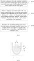
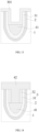
- Dynamic random access memories (DRAM) are widely applied to mobile devices such as mobile phones and tablet computers due to advantages of small size, high integration, and high transmission speed. As a core component of a DRAM, a word line structure is mainly used to control on or off of a transistor.
- During manufacturing of a word line structure, each film layer is usually etched by using a dry etching process. However, dry etching usually causes residues in a trench wall used for forming the word line structure, leading to structural defects, and further increasing a gate-induced drain leakage current.
- It should be noted that information disclosed in the above background section is used merely for a better understanding of the background of the present disclosure, and therefore may include information that does not constitute the prior art known to persons of ordinary skill in the art.
- An objective of the present disclosure is to overcome the foregoing deficiencies in the prior art, and provides a memory device, and a semiconductor structure and a forming method thereof, which can reduce a gate-induced drain leakage current, reduce power consumption, and improve device reliability.
- According to one aspect of the present disclosure, a method of forming a semiconductor structure is provided, including:
- providing a substrate, where the substrate includes a source region and a drain region spaced apart from each other, and a gate trench located between the source region and the drain region;
- forming, in sequence on an inner wall of the gate trench, a gate oxide layer, an interface layer, and a conductive layer that fills the gate trench; a thickness of a side of the interface layer away from the bottom of the gate trench being greater than a thickness of a side of the interface layer close to the bottom of the gate trench; and
- etching back the side of the interface layer away from the bottom of the gate trench by using a wet etching process, such that a top height of the interface layer is lower than a top height of the conductive layer.
- According to one aspect of the present disclosure, a semiconductor structure is provided, including:
- a substrate, wherein the substrate includes a source region and a drain region spaced apart from each other, and a gate trench located between the source region and the drain region; and
- a gate oxide layer, an interface layer and a conductive layer that fills the gate trench; wherein the gate oxide layer, the interface layer and the conductive layer are formed in sequence on an inner wall of the gate trench; a thickness of a side of the interface layer away from a bottom of the gate trench is greater than a thickness of a side of the interface layer close to the bottom of the gate trench; and a top height of the interface layer is lower than a top height of the conductive layer.
- According to one aspect of the present disclosure, a memory device is provided, including the semiconductor structure according to any one of the foregoing aspects.
- According to the memory device, and the semiconductor structure and a forming method thereof, an interface layer may be etched back by using a wet etching process, and an interface layer to be removed from a groove wall of a gate trench can be completely removed by isotropic etching, to avoid residuals and introduction of structural defects, thereby reducing a gate-induced drain leakage current. In addition, due to a greater thickness of the interface layer on a side away from the bottom of the gate trench, a wet etching area is relatively large during the etching back process, which facilitates execution of the wet etching process. In addition, a relatively large opening is formed after the etching back, such that the opening is subsequently filled with a dielectric with a relatively great thickness, thereby increasing a physical distance between a gate-drain overlapping region and a drain region, and further reducing the gate-induced drain leakage current. Further, the interface layer has a smaller thickness on a side close to the bottom of the gate trench, such that a resistance of the semiconductor structure can be reduced, power consumption can be reduced, and a capability of a gate to control the semiconductor structure can be improved.
- It should be understood that the above general description and the following detailed description are only exemplary and explanatory, and should not be construed as a limitation to the present disclosure.
- The accompanying drawings, which are incorporated into and constitute a part of the description, illustrate the embodiments of the present disclosure and together with the description, serve to explain the principles of the present disclosure. Apparently, the accompanying drawings in the following description show merely some embodiments of the present disclosure, and persons of ordinary skill in the art may still derive other drawings from these accompanying drawings without creative efforts.
-
FIG. 1 is a schematic diagram of a semiconductor structure in the related art. -
FIG. 2 is a schematic diagram of a gate trench in the related art. -
FIG. 3 is a schematic diagram of filling a gate oxide layer, an interface layer, and a conductive layer in the trench in the related art. -
FIG. 4 is a schematic diagram of a structure obtained after dry etching in the related art. -
FIG. 5 is a flowchart of a method of forming a semiconductor structure according to an implementation of the present disclosure. -
FIG. 6 is a schematic diagram of a semiconductor structure according to an implementation of the present disclosure. -
FIG. 7 is a schematic diagram of a gate trench according to an implementation of the present disclosure. -
FIG. 8 is a flowchart of step S120 according to an implementation of the present disclosure. -
FIG. 9 is a schematic diagram of a structure obtained after step S 1201 is completed according to an implementation of the present disclosure. -
FIG. 10 is a schematic diagram of a structure obtained after step S1202 is completed according to an implementation of the present disclosure. -
FIG. 11 is a schematic diagram of a structure obtained after step S1203 is completed according to an implementation of the present disclosure. -
FIG. 12 is a flowchart of step S1203 andstep S 1204 according to an implementation of the present disclosure. -
FIG. 13 is a schematic diagram of a structure obtained after step S210 is completed according to an implementation of the present disclosure. -
FIG. 14 is a schematic diagram of a structure obtained after step S230 is completed according to an implementation of the present disclosure. -
FIG. 15 is a schematic diagram of a structure obtained after step S240 is completed according to an implementation of the present disclosure. - 100. Substrate; 101. Drain; 102. Source; 103. Gate trench; 200. Word line structure; 201. Gate oxide layer; 202. Interface layer; 203. Conductive layer; 300. Bit line structure; 400. Storage capacitor; 500. Contact structure; 1. Substrate; 11. Gate trench; 2. Gate oxide layer; 3. Interface layer; 31. First interface layer; 32. Second interface layer; 301. Interface material; 4. Conductive layer; 41. First conductive material; 42. Second conductive material.
- Exemplary embodiments will be described below in further detail with reference to the accompanying drawings. However, the exemplary implementations can be implemented in various forms, and should not be construed as being limited to those described herein. On the contrary, these exemplary implementations are provided to make the present invention comprehensive and complete and to fully convey the concept manifested therein to those skilled in the art. The same reference numerals in the figures indicate the same or similar structures, and thus their detailed descriptions will be omitted.
- The foregoing described features, structures, or characteristics may be incorporated into one or more implementations in any suitable manner. If possible, the features discussed in the various embodiments are interchangeable. In the foregoing description, many specific details are provided to give a full understanding of the embodiments of the present invention. However, those skilled in the art will be aware that the technical solutions of the present invention may be practiced without one or more of the specific details, or other methods, materials, and the like may be used. In other cases, well-known structures, materials, or operations are not shown or described in detail to avoid obscuring aspects of the present invention.
- Although relative terms such as "upper" and "lower" are used in this specification to describe the relative relationship of one component of an icon to another, these terms are used in this specification only for convenience, for example, according to the orientation of the examples described in the accompanying drawings. It can be understood that if the device of the icon is turned upside down, the components described as "upper" will become the "lower" components. When a structure is "on" other structures, it may mean that the structure is integrally formed on other structures, or that the structure is "directly" disposed on other structures, or that the structure is "indirectly" disposed on other structures through another structure.
- The terms "one", "a", "the", "said", and "at least one" are used to indicate the presence of one or more elements/components/and the like; the terms "includes" and "has" are used to indicate an open-ended inclusion and to mean that additional elements/components/and the like may exist in addition to the listed elements/components/and the like. The terms "first" and "second" are used only as markers, not as a restriction on the number of objects.
- In the related art, as shown in
FIG. 1 , a memory device mainly includes asubstrate 100, aword line structure 200, abit line structure 300, astorage capacitor 400, and a transistor. Thebit line structure 300 is connected to adrain 101 of thesubstrate 100 through acontact structure 500. Theword line structure 200 serves as a gate of the transistor, to control on or off of the transistor. Thestorage capacitor 400 communicates with asource 102 of the transistor through thecontact structure 500. Theword line structure 200 mainly includes agate oxide layer 201, aninterface layer 202, and aconductive layer 203 that fills agate trench 103 that are formed on an inner wall of thegate trench 103. During manufacturing of theword line structure 200, as shown inFIG. 2 to FIG. 4 , thesubstrate 100 is first slotted to form thegate trench 103; then thegate trench 103 is filled with thegate oxide layer 201, theinterface layer 202, and theconductive layer 203; and then theinterface layer 202 located on the inner wall of thegate trench 103 is etched back by using a dry etching process. However, due to the limitation of the dry etching process, residues usually appear in the groove wall, causing structural defects and increasing a leakage current. In addition, an etching depth of dry etching is relatively difficult to control, making etch uniformity of adjacent semiconductor structures reduced, which in turn may lead to an increased gate-induced drain leakage current in some transistors. - An implementation of the present disclosure provides a method of forming a semiconductor structure. As shown in
FIG. 5 , the method of forming a semiconductor structure may include: - Step S110. Provide a substrate, where the substrate includes a source region and a drain region spaced apart from each other, and a gate trench located between the source region and the drain region.
- Step S120. Form, in sequence on an inner wall of the gate trench, a gate oxide layer, an interface layer, and a conductive layer that fills the gate trench, a thickness of a side of the interface layer away from the bottom of the gate trench is greater than a thickness of a side of the interface layer close to the bottom of the gate trench.
- Step S130. Etch back the side of the interface layer away from the bottom of the gate trench by using a wet etching process, such that the top height of the interface layer is lower than the top height of the conductive layer.
- In the method of forming a semiconductor structure in the present disclosure, an interface layer may be etched back by using a wet etching process, and an interface layer to be removed from a groove wall of a gate trench can be completely removed by isotropic etching, to avoid residuals and introduction of structural defects, thereby reducing a gate-induced drain leakage current. In addition, due to a greater thickness of the interface layer on a side away from the bottom of the gate trench, a wet etching area is relatively large during the etching back process, which facilitates execution of the wet etching process. In addition, a relatively large opening is formed after the etching back, such that the opening is subsequently filled with a dielectric with a relatively great thickness, thereby increasing a physical distance between a gate-drain overlapping region and a drain region, and further reducing the gate-induced drain leakage current. Further, the interface layer has a smaller thickness on a side close to the bottom of the gate trench, such that a resistance of the semiconductor structure can be reduced, and a capability of a gate to control the semiconductor structure can be improved.
- The steps of the method of forming a semiconductor structure in this implementation of the present disclosure are described in detail below:
As shown inFIG. 5 , in step S110, the substrate is provided, and the substrate includes the source region and the drain region spaced apart from each other, and the gate trench located between the source region and the drain region. - As shown in
FIG. 6 , a material of asubstrate 1 may be silicon or other semiconductor materials, and a shape and the material of thesubstrate 1 are not specially limited herein. A shallow trench isolation structure, a well region, or the like may also be formed on thesubstrate 1. Thesubstrate 1 may be P-type, and may include a source region and a drain region spaced apart from each other. The source region and the drain region may be doped to form a source and a drain. For example, the source region and the drain region may be n-type doped. For example, the source region and the drain region may be doped with an n-type doping material, such that an n-type semiconductor is formed in the source region and the drain region. The n-type doping material may be an element in the IV main group of the periodic table. For example, the n-type doping material may be phosphorus, or certainly, may be a material of other elements, which are not be listed herein. - In an embodiment, phosphorus ions may be injected into the source region and the drain region by ion implantation. Certainly, other processes may be used to dope the source region and/or the drain region. This is not specially limited herein.
- It should be noted that, a trench region may be located between the source region and the drain region, and there may be a
gate trench 11 in the trench region. As shown inFIG. 7 , a buried word line structure may be formed in thegate trench 11, and the word line structure serves as a gate of a transistor and can control on or off of the transistor. - For example, the trench region in the
substrate 1 may be patterned to form thegate trench 11. For example, a photoresist may be formed on a surface of thesubstrate 1, and a mask plate may be used to expose the photoresist to form a developing region. A pattern of the developing region may be the same as a pattern required by thegate trench 11. Non-isotropic etching may be performed on the developing region by using a dry etching process, to form thegate trench 11. - In an implementation, a side wall of the
gate trench 11 may extend along a direction perpendicular to thesubstrate 1. The bottom of thegate trench 11 may be in a shape of an arc, and an arc center thereof may be located in thegate trench 11. The side wall of thegate trench 11 may be connected to two ends of the arc. Thegate trench 11 may have a depth of 100 nm to 300 nm. For example, the depth may be 100 nm, 150 nm, 200 nm, 250 nm, or 300 nm. Thegate trench 11 may have a width of 10 nm to 50 nm. For example, the width may be 10 nm, 20 nm, 30 nm, 40 nm, or 50 nm. Certainly, thegate trench 11 may be of other sizes, which is not specially limited herein. It should be noted that, the width of thegate trench 11 may be a lateral dimension between side walls of thegate trench 11. - As shown in
FIG. 5 , in step S120, the gate oxide layer, the interface layer, and the conductive layer that fills the gate trench are formed in sequence on the inner wall of the gate trench, the thickness of the side of the interface layer away from the bottom of the gate trench is greater than the thickness of the side of the interface layer close to the bottom of the gate trench. - A fittedly attached
gate oxide layer 2 and a fittedly attachedinterface layer 3 may be formed on the side wall and a bottom surface of thegate trench 11. Thegate oxide layer 2 may be located between theinterface layer 3 and the inner wall of thegate trench 11. In addition, aconductive layer 4 may be formed on a side of theinterface layer 3 away from thegate oxide layer 2, and theconductive layer 4 can fill thegate trench 11. Arranging theinterface layer 3 between thegate oxide layer 2 and theconductive layer 4 can adjust a work function of the device. - The thickness of the side of the
interface layer 3 away from the bottom of thegate trench 11 may be greater than the thickness of the side of theinterface layer 3 close to the bottom of thegate trench 11, and theconductive layer 4 and theinterface layer 3 located at different depths of thegate trench 11 are in close contact with each other. The relatively small thickness of theinterface layer 3 around theconductive layer 4 located on the side close to the bottom of thegate trench 11 can help reduce the resistance. In addition, due to a greater thickness of theinterface layer 3 around theconductive layer 4 located on the side away from the bottom of thegate trench 11, a wet etching area is relatively large during a subsequent etching back process, which facilitates execution of the wet etching process. In addition, a relatively large opening is formed after the etching back, such that the opening is subsequently filled with a dielectric with a relatively great thickness, thereby increasing a physical distance between a gate-drain overlapping region and a drain region, and further reducing a gate-induced drain leakage current. - In an implementation of the present disclosure, step S120 may include step S1201 to step S1204, as shown in
FIG. 8 :
Step S1201. Form, in sequence on the inner wall of the gate trench, a fittedly attached gate oxide layer, a fittedly attached first interface layer, and a first conductive material that fills the gate trench. - As shown in
FIG. 9 , thegate oxide layer 2, afirst interface layer 31, and a firstconductive material 41 may be formed in thegate trench 11 in a manner such as chemical vapor deposition, physical vapor deposition, thermal oxidation, vacuum evaporation, magnetron sputtering, or atomic layer deposition. Thegate oxide layer 2 and thefirst interface layer 31 may be fittedly attached to the inner wall of thegate trench 11 in sequence. The firstconductive material 41 may be formed on a side of thefirst interface layer 31 away from thegate oxide layer 2 and can fill thegate oxide layer 2. - For example, the fittedly attached
gate oxide layer 2 may be formed on the inner wall of thegate trench 11 in a manner such as chemical vapor deposition, thermal oxidation, or atomic layer deposition. In addition, for process convenience, thegate oxide layer 2 can completely cover a top surface of thegate trench 11 during the formation process, and thegate oxide layer 2 located on the top surface of thegate trench 11 can be removed subsequently. Certainly, thegate oxide layer 2 may be formed in other manners. This is not specially limited herein. - A material of the
gate oxide layer 2 may include silicon oxide, silicon nitride, silicon oxynitride, or other high-k dielectric materials, or may be a combination of the foregoing materials. The thickness of thegate oxide layer 2 may be 1 nm to 6 nm. For example, the thickness may be 1 nm, 2 nm, 3 nm, 4 nm, 5 nm, or 6 nm. Certainly, the thicknesses of thegate oxide layer 2 may be other values, which are not listed herein. - The
first interface layer 31 may be fittedly attached to a surface of thegate oxide layer 2, a material of thefirst interface layer 31 may be titanium nitride, and a thickness of thefirst interface layer 31 may be 0.5 nm to 2 nm, for example, may be 0.5 nm, 1 nm, 1.5 nm, or 2 nm. In some embodiments, thefirst interface layer 31 may be formed on thegate oxide layer 2 by using a process such as chemical vapor deposition, physical vapor deposition, or atomic layer deposition. A forming process of thefirst interface layer 31 is not specially limited herein. - The first
conductive material 41 may be deposited on the surface of thefirst interface layer 31. The firstconductive material 41 can fill thegate trench 11. The firstconductive material 41 may be metal tungsten. The firstconductive material 41 may be formed on the surface of thefirst interface layer 31 by using a process such as vacuum evaporation, magnetron sputtering, or atomic layer deposition. - Step S1202. Etch the first conductive material by using a dry etching process, to expose a part of the first interface layer located on a side wall of the gate trench.
- As shown in
FIG. 10 , non-isotropic etching may be performed on the firstconductive material 41 by using the dry etching process, to remove part of the firstconductive material 41, to expose a part of thefirst interface layer 31 located on the side wall of thegate trench 11. An etching depth of the firstconductive material 41 may be 5 nm to 70 nm. For example, the etching depth may be 5 nm, 10 nm, 30 nm, 50 nm, or 70 nm, or certainly, may be other values, which are not listed herein. - During the etching of the first
conductive material 41, an optical critical dimension (OCD) may be used to monitor the etching depth of the firstconductive material 41, to accurately control the etching depth during the etching process. For example, during the etching process, the firstconductive material 41 may be preliminarily etched. After the preliminary etching is completed, the OCD may be used to measure the etching depth, and determine whether the etching depth meets a process requirement. When the etching depth does not meet an etching depth requirement, the firstconductive material 41 may be further etched, the etching depth thereof may be measured, and the etching stops until a detected depth meets the depth requirement. - Step S1203. Form a second interface layer on a surface of the first interface layer located on the side wall of the gate trench, where the first interface layer and the second interface layer constitute the interface layer.
- As shown in
FIG. 11 , after the firstconductive material 41 is etched, asecond interface layer 32 may be formed on a surface of thefirst interface layer 31 exposed on the side wall of thegate trench 11. A side of thesecond interface layer 32 close to the bottom of thegate trench 11 may be in contact with a surface of the remaining firstconductive material 41, and thefirst interface layer 31 and thesecond interface layer 32 may constitute theinterface layer 3, such that the thickness of theinterface layer 3 formed on a side close to the bottom of thegate trench 11 is smaller than the thickness of theinterface layer 3 formed on a side away from the bottom of thegate trench 11. Because the thickness of theinterface layer 3 on the side close to the bottom of thegate trench 11 is smaller, a resistance can be reduced and power consumption can be reduced. - In an implementation of the present disclosure, the forming a
second interface layer 32 on a surface of thefirst interface layer 31 located on the side wall of thegate trench 11, that is, step S1203, may include step S210 and step S220, as shown inFIG. 12 :
Step S210. Deposit an interface material on a surface of a structure constituted by the first conductive material, the first interface layer, and the gate oxide layer. - As shown in
FIG. 13 , aninterface material 301 may be formed on a surface of a structure constituted by the firstconductive material 41, thefirst interface layer 31, and thegate oxide layer 2. For process convenience, theinterface material 301 may cover the source region and the drain region. The material of theinterface material 301 may be the same as the material of thefirst interface layer 31. For example, the material may be titanium nitride. Theinterface material 301 may be deposited by using a process such as chemical vapor deposition, physical vapor deposition, or atomic layer deposition. Certainly, theinterface material 301 may alternatively be formed in other manners, which are not listed herein. - Step S220. Remove the interface material located on a region other than the side wall of the gate trench by using the dry etching process to form the second interface layer.
- An
interface material 301 located on a region other than the side wall of thegate trench 11 may be removed by using a process such as chemical polishing and dry etching to form thesecond interface layer 32. That is, theinterface material 301 located on the top surface of thegate trench 11 and the surface of the firstconductive material 41 is removed, only theinterface material 301 located on the side wall of thegate trench 11 remains, and the remaininginterface material 301 may be in contact with the surface of the firstconductive material 41. - A thickness of the
second interface layer 32 may be 2 nm to 10 nm. For example, the thickness may be 2 nm, 4 nm, 6 nm, 8 nm, or 10 nm, or certainly, may be other values, which are not listed herein. It should be noted that, a thickness of an overlapping part of thefirst interface layer 31 and thesecond interface layer 32 may be greater than 4 nm, such that an electric field between the drain region and theconductive layer 4 can be reduced, and a drain leakage current can be reduced, thereby improving structural reliability. - Step S1204. Deposit a second conductive material on a surface of the first conductive material away from the gate oxide layer, and wrap the second interface layer around a periphery of the second conductive material.
- After the
second interface layer 32 is formed, the secondconductive material 42 may be deposited on a side of the firstconductive material 41 away from thegate oxide layer 2, the secondconductive material 42 may fill thegate trench 11 and may be in contact with thesecond interface layer 32. In this case, thesecond interface layer 32 may be wrapped around a periphery of the secondconductive material 42. In addition, because thefirst interface layer 31 is located on a side of thesecond interface layer 32 away from the secondconductive material 42, thefirst interface layer 31 and thesecond interface layer 32 constitute the interface layer, such that a thickness of theinterface layer 3 located on the periphery of the secondconductive material 42 is increased, thereby increasing a physical size between the secondconductive material 42 and the source drain, reducing an electric field between the drain region and the secondconductive material 42, reducing a drain leakage current, and improving structural reliability. - The material of the second
conductive material 42 may be the same as the material of the firstconductive material 41. For example, the material may be metal tungsten, or certainly, may be other conductive materials. This is not specially limited herein. - In an implementation of the present disclosure, the depositing a second
conductive material 42 on a surface of the firstconductive material 41 away from thegate oxide layer 2, and wrapping thesecond interface layer 32 around a periphery of the second conductive material 42 (that is, step S1204) may include step S230 and step S240:
Step S230. Deposit the second conductive material on a side of the first conductive material away from the gate oxide layer, and the second conductive material covers the second interface layer. - As shown in
FIG. 14 , the secondconductive material 42 may be deposited on the side of the firstconductive material 41 away from thegate oxide layer 2 in a manner such as vacuum evaporation, magnetron sputtering, chemical vapor deposition, or atomic layer deposition. In order to ensure that the secondconductive material 42 is in full contact with thesecond interface layer 32, during the filling process, the secondconductive material 42 may be made to fill thegate trench 11 and overflow. - Step S240. Remove the second conductive material overflowing the gate trench by using the dry etching process, where the first conductive material and the second conductive material constitute the conductive layer.
- As shown in
FIG. 15 , the secondconductive material 42 overflowing thegate trench 11 may be removed by using a dry etching process, or the secondconductive material 42 overflowing thegate trench 11 may be removed by using a chemical polishing process. This is not specially limited herein. During the removal of the secondconductive material 42 overflowing thegate trench 11, the top surface of the secondconductive material 42 may be made lower than an opening of thegate trench 11, to prevent the secondconductive material 42 from being short-circuited due to communication with another component in thegate trench 11. - It should be noted that, the first
conductive material 41 and the secondconductive material 42 can constitute theconductive layer 4, and the firstconductive material 41 and the secondconductive material 42 can be integrally formed when process conditions permit. - As shown in
FIG. 5 , in step S130, the side of the interface layer away from the bottom of the gate trench is etched back by using the wet etching process, such that the top height of the interface layer is lower than the top height of the conductive layer. - The
interface layer 3 wrapped around the periphery of theconductive layer 4 may be etched back by using the wet etching process, such that the top height of theinterface layer 3 is lower than the top height of theconductive layer 4, and a distance of a gate-drain overlapping region is increased, thereby reducing a gate-induced drain leakage current. In this process, theinterface layer 3 to be removed from a groove wall of thegate trench 11 can be completely removed by isotropic etching, to avoid residuals, thereby reducing a gate-induced drain leakage current; and avoid use of an additional cleaning process to clean residues, such that manufacturing costs can be reduced. - In an implementation, an etching back depth the
interface layer 3 relative to the surface of thesubstrate 1 may be 5 nm to 50 nm. For example, the depth may be 5 nm, 10 nm, 20 nm, 30 nm, 40 nm, or 50 nm, an etching back depth theinterface layer 3 relative to a top surface of theconductive layer 4 may be 1 nm to 30 nm. For example, the depth may be 1 nm, 5 nm, 10 nm, 15 nm, 20 nm, 25 nm, or 30 nm. Certainly, the etching back depth may have other values, which are not listed herein. During the etching back process, an OCD may be used to monitor the etching depth of theinterface layer 3, to accurately control the etching back depth of theinterface layer 3, such that etching back uniformity of theinterface layer 3 in adjacent semiconductor structures can be improved. For example, during the etching process, theinterface layer 3 may be preliminarily etched. After the preliminary etching is completed, the OCD may be used to measure the etching depth, and determine whether the etching depth meets a process requirement. When the etching depth does not meet an etching depth requirement, theinterface layer 3 may be further etched, the etching depth thereof may be measured, and the etching stops until a detected depth meets the depth requirement. - In an implementation, the
interface layer 3 may be etched by using a selective wet etching process. For example, theinterface layer 3 may be selectively etched by using an etching solution to avoid damage to other film layers. Specifically, a corrosive solution may be used to selectively etch theinterface layer 3. The corrosive solution may be a mixture of hydrogen peroxide and sulfuric acid. A mixture ratio thereof may range from 1:5 to 1:20, where the hydrogen peroxide accounts for 1 and the sulfuric acid accounts for 5 to 20. - For example, during the etching back process of the
interface layer 3, an etching selectivity of theinterface layer 3 and theconductive layer 4 may be 5 to 40, for example, may be 5, 10, 20, 30, or 40, or certainly, may be other values, which are not listed herein. For example, when the etching selectivity of theinterface layer 3 and theconductive layer 4 may be 40, 1 nm of theconductive layer 4 is etched each time 40 nm of theinterface layer 3 is etched. - An embodiment of the present disclosure further provides a semiconductor structure. The semiconductor structure may include a
substrate 1, agate oxide layer 2, aninterface layer 3, and aconductive layer 4. - The
substrate 1 may include a source region and a drain region spaced apart from each other, and agate trench 11 located between the source region and the drain region. - The
gate oxide layer 2 and theinterface layer 3 are formed in sequence on the inner wall of thegate trench 11. Theconductive layer 4 fills thegate trench 11. A side of theconductive layer 4 close to the bottom of thegate trench 11 has a larger width than a side of theconductive layer 4 away from the bottom of thegate trench 11. A thickness of a side of theinterface layer 3 away from the bottom of thegate trench 11 is greater than a thickness of a side of theinterface layer 3 close to the bottom of thegate trench 11, and the top height of theinterface layer 3 is lower than the top height of theconductive layer 4. - The specific details, forming process, and beneficial effects of the part in the semiconductor structure have been described in detail in the corresponding method of forming the semiconductor structure. Therefore, details are not described herein again. For example, the semiconductor structure of the present disclosure may be a buried word line structure, and the word line structure may serve as a gate of a transistor and can control on or off of the transistor.
- An embodiment of the present disclosure further provides a memory device. The memory device may include the semiconductor structure in any one of the foregoing implementations. The specific details and beneficial effects of the semiconductor structure have been described in detail in the corresponding embodiment of the semiconductor structure. Therefore, details are not described herein again.
- The memory device may be a DRAM, or certainly, may be other storage apparatuses, which are not listed herein.
- Those skilled in the art may easily figure out other implementations of the present disclosure after considering the specification and practicing the invention disclosed herein. The present disclosure is intended to cover any variations, purposes or adaptive changes of the present disclosure. Such variations, purposes or applicable changes follow the general principle of the present disclosure and include common knowledge or conventional technical means in the technical field which is not disclosed in the present disclosure. The specification and embodiments are merely considered as illustrative, and the real scope and spirit of the present disclosure are pointed out by the appended claims.
Claims (16)
- A method of forming a semiconductor structure, comprising:providing a substrate, wherein the substrate comprises a source region and a drain region spaced apart from each other, and a gate trench located between the source region and the drain region;forming, in sequence on an inner wall of the gate trench, a gate oxide layer, an interface layer, and a conductive layer that fills the gate trench; a thickness of a side of the interface layer away from a bottom of the gate trench being greater than a thickness of a side of the interface layer close to the bottom of the gate trench; andetching back the side of the interface layer away from the bottom of the gate trench by using a wet etching process, such that a top height of the interface layer is lower than a top height of the conductive layer.
- The method of forming a semiconductor structure according to claim 1, wherein the forming, in sequence on an inner wall of the gate trench, a gate oxide layer, an interface layer, and a conductive layer that fills the gate trench; a thickness of a side of the interface layer away from a bottom of the gate trench being greater than a thickness of a side of the interface layer close to the bottom of the gate trench comprises:forming, in sequence on the inner wall of the gate trench, a fittedly attached gate oxide layer and a fittedly attached first interface layer, and a first conductive material that fills the gate trench;etching the first conductive material by using a dry etching process, to expose a part of the first interface layer located on a side wall of the gate trench;forming a second interface layer on a surface of the first interface layer located on the side wall of the gate trench, wherein the first interface layer and the second interface layer constitute the interface layer; anddepositing a second conductive material on a surface of the first conductive material away from the gate oxide layer, and wrapping the second interface layer around a periphery of the second conductive material.
- The method of forming a semiconductor structure according to claim 1, wherein the etching back the side of the interface layer away from the bottom of the gate trench by using a wet etching process, such that a top height of the interface layer is lower than a top height of the conductive layer comprises:
etching the interface layer by using a selective wet etching process, such that the top height of the interface layer is lower than the top height of the conductive layer. - The method of forming a semiconductor structure according to claim 3, wherein an etching selectivity of the interface layer to the conductive layer is 5 to 40.
- The method of forming a semiconductor structure according to claim 2, wherein a depth of the gate trench is 100 nm to 300 nm, and a width of the gate trench is 10 nm to 50 nm.
- The method of forming a semiconductor structure according to claim 5, wherein an etching depth of the first conductive material is 5 nm to 70 nm, and an etching back depth of the interface layer is 5 nm to 50 nm.
- The method of forming a semiconductor structure according to claim 2, wherein the forming a second interface layer on a surface of the first interface layer located on the side wall of the gate trench comprises:depositing an interface material on a surface of a structure constituted by the first conductive material, the first interface layer, and the gate oxide layer; andremoving the interface material located on a region other than the side wall of the gate trench by using the dry etching process to form the second interface layer.
- The method of forming a semiconductor structure according to claim 2, wherein the depositing a second conductive material on a surface of the first conductive material away from the gate oxide layer, and wrapping the second interface layer around a periphery of the second conductive material comprises:depositing the second conductive material on a side of the first conductive material away from the gate oxide layer, wherein the second conductive material covers the second interface layer; andremoving the second conductive material overflowing the gate trench by using the dry etching process, wherein the first conductive material and the second conductive material constitute the conductive layer.
- The method of forming a semiconductor structure according to claim 2, wherein a material of the first conductive material is the same as a material of the second conductive material.
- The method of forming a semiconductor structure according to claim 2, wherein a thickness of the first interface layer is 0.5 nm to 2 nm, and a thickness of the second interface layer is 2 nm to 10 nm.
- A semiconductor structure, comprising:a substrate, wherein the substrate comprises a source region and a drain region spaced apart from each other, and a gate trench located between the source region and the drain region; anda gate oxide layer, an interface layer and a conductive layer that fills the gate trench;wherein the gate oxide layer, the interface layer and the conductive layer are formed in sequence on an inner wall of the gate trench; a thickness of a side of the interface layer away from a bottom of the gate trench is greater than a thickness of a side of the interface layer close to the bottom of the gate trench; and a top height of the interface layer is lower than a top height of the conductive layer.
- The semiconductor structure according to claim 11, wherein the interface layer comprises a first interface layer and a second interface layer, the first interface layer is fittedly attached to a side of the gate oxide layer away from the inner wall of the gate trench, and the second interface layer is formed on a surface of the first interface layer located on a side wall of the gate trench; and the conductive layer comprises a first conductive material and a second conductive material, the first conductive material fills the gate trench and is in contact with the first interface layer, the second conductive material is formed on a side of the first conductive material away from the gate oxide layer, and the second interface layer is wrapped around a periphery of the second conductive material.
- The semiconductor structure according to claim 12, wherein a material of the first conductive material is the same as a material of the second conductive material.
- The semiconductor structure according to claim 11, wherein a depth of the gate trench is 100 nm to 300 nm, and a width of the gate trench is 10 nm to 50 nm.
- The semiconductor structure according to claim 12, wherein a thickness of the first interface layer is 0.5 nm to 2 nm, and a thickness of the second interface layer is 2 nm to 10 nm.
- A memory device, comprising the semiconductor structure according to any one of claims 11 to 15.
Applications Claiming Priority (2)
| Application Number | Priority Date | Filing Date | Title |
|---|---|---|---|
| CN202110067276.1A CN114823310A (en) | 2021-01-19 | 2021-01-19 | Memory device, semiconductor structure and forming method thereof |
| PCT/CN2021/112022 WO2022156194A1 (en) | 2021-01-19 | 2021-08-11 | Memory device, and semiconductor structure and forming method therefor |
Publications (2)
| Publication Number | Publication Date |
|---|---|
| EP4199042A1 true EP4199042A1 (en) | 2023-06-21 |
| EP4199042A4 EP4199042A4 (en) | 2024-06-12 |
Family
ID=82405364
Family Applications (1)
| Application Number | Title | Priority Date | Filing Date |
|---|---|---|---|
| EP21920574.7A Pending EP4199042A4 (en) | 2021-01-19 | 2021-08-11 | Memory device, and semiconductor structure and forming method therefor |
Country Status (2)
| Country | Link |
|---|---|
| US (1) | US12295135B2 (en) |
| EP (1) | EP4199042A4 (en) |
Families Citing this family (2)
| Publication number | Priority date | Publication date | Assignee | Title |
|---|---|---|---|---|
| US20240186318A1 (en) * | 2022-12-02 | 2024-06-06 | Stmicroelectronics (Rousset) Sas | Integrated circuit comprising a capacitive transistor |
| CN119342859A (en) * | 2024-10-10 | 2025-01-21 | 浙江创芯集成电路有限公司 | Semiconductor structure and method for forming the same, and storage array |
Family Cites Families (19)
| Publication number | Priority date | Publication date | Assignee | Title |
|---|---|---|---|---|
| US5241193A (en) | 1992-05-19 | 1993-08-31 | Motorola, Inc. | Semiconductor device having a thin-film transistor and process |
| KR100604816B1 (en) * | 2003-05-19 | 2006-07-28 | 삼성전자주식회사 | Method for manufacturing integrated circuit device recess transistor and integrated circuit device recess transistor manufactured thereby |
| DE102005026228B4 (en) | 2004-06-08 | 2010-04-15 | Samsung Electronics Co., Ltd., Suwon | GAA type transistor and method of making the same |
| JP4552603B2 (en) * | 2004-11-08 | 2010-09-29 | エルピーダメモリ株式会社 | Manufacturing method of semiconductor device |
| KR100668862B1 (en) | 2005-10-25 | 2007-01-16 | 주식회사 하이닉스반도체 | Recess channel transistor and its formation method |
| US8115251B2 (en) * | 2007-04-30 | 2012-02-14 | International Business Machines Corporation | Recessed gate channel with low Vt corner |
| US8039381B2 (en) | 2008-09-12 | 2011-10-18 | Taiwan Semiconductor Manufacturing Company, Ltd. | Photoresist etch back method for gate last process |
| KR101088816B1 (en) | 2009-06-04 | 2011-12-02 | 주식회사 하이닉스반도체 | Semiconductor device and manufacturing method thereof |
| KR101186011B1 (en) | 2009-11-27 | 2012-09-25 | 에스케이하이닉스 주식회사 | Semiconductor device and method for forming the same |
| US8211775B1 (en) | 2011-03-09 | 2012-07-03 | United Microelectronics Corp. | Method of making transistor having metal gate |
| KR102181609B1 (en) * | 2014-02-04 | 2020-11-23 | 삼성전자주식회사 | Semiconductor device and fabricating method thereof |
| KR102250583B1 (en) * | 2014-12-16 | 2021-05-12 | 에스케이하이닉스 주식회사 | Semiconductor device having dual work function gate structure and method for manufacturing the same, memory cell having the same and electronic device having the same |
| CN105990137B (en) | 2015-01-30 | 2019-08-27 | 中芯国际集成电路制造(上海)有限公司 | Transistor and forming method thereof, semiconductor structure and forming method thereof |
| KR102481478B1 (en) * | 2016-06-16 | 2022-12-26 | 삼성전자 주식회사 | Semiconductor devices and method of forming the same |
| US9991362B2 (en) * | 2016-09-30 | 2018-06-05 | Taiwan Semiconductor Manufacturing Co., Ltd. | Semiconductor device including tungsten gate and manufacturing method thereof |
| CN108110005A (en) | 2017-12-07 | 2018-06-01 | 睿力集成电路有限公司 | Transistor arrangement, memory cell array and preparation method thereof |
| US11031478B2 (en) * | 2018-01-23 | 2021-06-08 | Infineon Technologies Austria Ag | Semiconductor device having body contacts with dielectric spacers and corresponding methods of manufacture |
| KR102457515B1 (en) * | 2018-02-22 | 2022-10-21 | 에스케이하이닉스 주식회사 | Semiconductor device having buried gate structure and method for manufacturing the same |
| US10790287B2 (en) | 2018-11-29 | 2020-09-29 | Applied Materials, Inc. | Reducing gate induced drain leakage in DRAM wordline |
-
2021
- 2021-08-11 EP EP21920574.7A patent/EP4199042A4/en active Pending
-
2022
- 2022-03-28 US US17/656,769 patent/US12295135B2/en active Active
Also Published As
| Publication number | Publication date |
|---|---|
| US12295135B2 (en) | 2025-05-06 |
| EP4199042A4 (en) | 2024-06-12 |
| US20220231028A1 (en) | 2022-07-21 |
Similar Documents
| Publication | Publication Date | Title |
|---|---|---|
| US8664075B2 (en) | High capacitance trench capacitor | |
| KR0167811B1 (en) | Dynamic Random Access Memory Cell Manufacturing Method | |
| KR102838573B1 (en) | Semiconductor device and method for fabricating thereof | |
| US8580669B2 (en) | Method for fabricating semiconductor device | |
| US7504296B2 (en) | Semiconductor memory device and method for fabricating the same | |
| US20070045699A1 (en) | Method of fabricating a trench capacitor having increased capacitance | |
| KR20100057203A (en) | Wiring structure of semiconductor device and method of forming a wiring structure | |
| US12295135B2 (en) | Memory device, and semiconductor structure and forming method thereof | |
| CN106158751A (en) | The manufacture method of dynamic random access memory device | |
| US5843819A (en) | Semiconductor memory device with trench capacitor and method for the production thereof | |
| KR101205067B1 (en) | Method for fabricating semiconductor device | |
| US10043812B1 (en) | Semiconductive structure with word line and method of fabricating the same | |
| WO2021227731A1 (en) | Manufacturing method for buried word line structure, and semiconductor memory comprising buried word line structure | |
| US5913129A (en) | Method of fabricating a capacitor structure for a dynamic random access memory | |
| WO2022156194A1 (en) | Memory device, and semiconductor structure and forming method therefor | |
| JPH08213568A (en) | Semiconductor memory device and its manufacture | |
| US12593435B2 (en) | eDRAM and method for making same | |
| WO2022062717A1 (en) | Semiconductor structure forming method and semiconductor structure | |
| US11690217B2 (en) | Dynamic random access memory with adhesion layer and method of manufacturing the same | |
| US6924204B2 (en) | Split gate flash memory cell and manufacturing method thereof | |
| WO2024103851A1 (en) | Semiconductor structure and forming method therefor, and memory | |
| KR100906646B1 (en) | Semiconductor memory device and manufacturing method thereof | |
| CN117794237B (en) | Semiconductor structure and its formation method, memory | |
| US20260113928A1 (en) | Semiconductor structure and method of manufacturing the same | |
| EP4350736A1 (en) | Semiconductor structure, forming method therefor, and memory |
Legal Events
| Date | Code | Title | Description |
|---|---|---|---|
| STAA | Information on the status of an ep patent application or granted ep patent |
Free format text: STATUS: THE INTERNATIONAL PUBLICATION HAS BEEN MADE |
|
| PUAI | Public reference made under article 153(3) epc to a published international application that has entered the european phase |
Free format text: ORIGINAL CODE: 0009012 |
|
| STAA | Information on the status of an ep patent application or granted ep patent |
Free format text: STATUS: REQUEST FOR EXAMINATION WAS MADE |
|
| 17P | Request for examination filed |
Effective date: 20230317 |
|
| AK | Designated contracting states |
Kind code of ref document: A1 Designated state(s): AL AT BE BG CH CY CZ DE DK EE ES FI FR GB GR HR HU IE IS IT LI LT LU LV MC MK MT NL NO PL PT RO RS SE SI SK SM TR |
|
| DAV | Request for validation of the european patent (deleted) | ||
| DAX | Request for extension of the european patent (deleted) | ||
| A4 | Supplementary search report drawn up and despatched |
Effective date: 20240510 |
|
| RIC1 | Information provided on ipc code assigned before grant |
Ipc: H01L 29/49 20060101ALI20240503BHEP Ipc: H01L 29/78 20060101ALI20240503BHEP Ipc: H01L 29/66 20060101ALI20240503BHEP Ipc: H01L 29/423 20060101ALI20240503BHEP Ipc: H10B 12/00 20230101ALI20240503BHEP Ipc: H01L 21/28 20060101AFI20240503BHEP |
|
| STAA | Information on the status of an ep patent application or granted ep patent |
Free format text: STATUS: EXAMINATION IS IN PROGRESS |
|
| 17Q | First examination report despatched |
Effective date: 20250213 |
|
| REG | Reference to a national code |
Ref country code: DE Ref legal event code: R079 Free format text: PREVIOUS MAIN CLASS: H01L0021280000 Ipc: H10D0064010000 |
|
| GRAP | Despatch of communication of intention to grant a patent |
Free format text: ORIGINAL CODE: EPIDOSNIGR1 |
|
| STAA | Information on the status of an ep patent application or granted ep patent |
Free format text: STATUS: GRANT OF PATENT IS INTENDED |
|
| RIC1 | Information provided on ipc code assigned before grant |
Ipc: H10D 64/01 20250101AFI20260112BHEP Ipc: H10B 12/00 20230101ALI20260112BHEP Ipc: H10D 30/01 20250101ALI20260112BHEP Ipc: H10D 30/60 20250101ALI20260112BHEP Ipc: H10D 64/27 20250101ALI20260112BHEP Ipc: H10D 64/66 20250101ALI20260112BHEP |
|
| INTG | Intention to grant announced |
Effective date: 20260121 |
|
| P01 | Opt-out of the competence of the unified patent court (upc) registered |
Free format text: CASE NUMBER: UPC_APP_0009310_4199042/2026 Effective date: 20260311 |