EP4198676A1 - Voltage regulation using a delta-sigma modulator, device and method - Google Patents
Voltage regulation using a delta-sigma modulator, device and method Download PDFInfo
- Publication number
- EP4198676A1 EP4198676A1 EP21306831.5A EP21306831A EP4198676A1 EP 4198676 A1 EP4198676 A1 EP 4198676A1 EP 21306831 A EP21306831 A EP 21306831A EP 4198676 A1 EP4198676 A1 EP 4198676A1
- Authority
- EP
- European Patent Office
- Prior art keywords
- delta
- signal
- voltage regulator
- power
- sigma
- Prior art date
- Legal status (The legal status is an assumption and is not a legal conclusion. Google has not performed a legal analysis and makes no representation as to the accuracy of the status listed.)
- Pending
Links
Images




Classifications
-
- G—PHYSICS
- G05—CONTROLLING; REGULATING
- G05F—SYSTEMS FOR REGULATING ELECTRIC OR MAGNETIC VARIABLES
- G05F1/00—Automatic systems in which deviations of an electric quantity from one or more predetermined values are detected at the output of the system and fed back to a device within the system to restore the detected quantity to its predetermined value or values, i.e. retroactive systems
- G05F1/10—Regulating voltage or current
- G05F1/46—Regulating voltage or current wherein the variable actually regulated by the final control device is DC
- G05F1/56—Regulating voltage or current wherein the variable actually regulated by the final control device is DC using semiconductor devices in series with the load as final control devices
- G05F1/561—Voltage to current converters
-
- G—PHYSICS
- G05—CONTROLLING; REGULATING
- G05F—SYSTEMS FOR REGULATING ELECTRIC OR MAGNETIC VARIABLES
- G05F1/00—Automatic systems in which deviations of an electric quantity from one or more predetermined values are detected at the output of the system and fed back to a device within the system to restore the detected quantity to its predetermined value or values, i.e. retroactive systems
- G05F1/10—Regulating voltage or current
- G05F1/46—Regulating voltage or current wherein the variable actually regulated by the final control device is DC
- G05F1/56—Regulating voltage or current wherein the variable actually regulated by the final control device is DC using semiconductor devices in series with the load as final control devices
- G05F1/575—Regulating voltage or current wherein the variable actually regulated by the final control device is DC using semiconductor devices in series with the load as final control devices characterised by the feedback circuit
-
- G—PHYSICS
- G05—CONTROLLING; REGULATING
- G05F—SYSTEMS FOR REGULATING ELECTRIC OR MAGNETIC VARIABLES
- G05F1/00—Automatic systems in which deviations of an electric quantity from one or more predetermined values are detected at the output of the system and fed back to a device within the system to restore the detected quantity to its predetermined value or values, i.e. retroactive systems
- G05F1/10—Regulating voltage or current
- G05F1/46—Regulating voltage or current wherein the variable actually regulated by the final control device is DC
- G05F1/56—Regulating voltage or current wherein the variable actually regulated by the final control device is DC using semiconductor devices in series with the load as final control devices
- G05F1/59—Regulating voltage or current wherein the variable actually regulated by the final control device is DC using semiconductor devices in series with the load as final control devices including plural semiconductor devices as final control devices for a single load
-
- H—ELECTRICITY
- H03—ELECTRONIC CIRCUITRY
- H03M—CODING; DECODING; CODE CONVERSION IN GENERAL
- H03M3/00—Conversion of analogue values to or from differential modulation
- H03M3/30—Delta-sigma modulation
- H03M3/39—Structural details of delta-sigma modulators, e.g. incremental delta-sigma modulators
- H03M3/412—Structural details of delta-sigma modulators, e.g. incremental delta-sigma modulators characterised by the number of quantisers and their type and resolution
- H03M3/422—Structural details of delta-sigma modulators, e.g. incremental delta-sigma modulators characterised by the number of quantisers and their type and resolution having one quantiser only
- H03M3/424—Structural details of delta-sigma modulators, e.g. incremental delta-sigma modulators characterised by the number of quantisers and their type and resolution having one quantiser only the quantiser being a multiple bit one
- H03M3/428—Structural details of delta-sigma modulators, e.g. incremental delta-sigma modulators characterised by the number of quantisers and their type and resolution having one quantiser only the quantiser being a multiple bit one with lower resolution, e.g. single bit, feedback
Definitions
- the present disclosure relates to a voltage regulation device that comprises a digital modulation device with a delta-sigma, a quantizer, and a feedforward path. Further, the present disclosure relates to a method of operating the voltage regulation device. Furthermore, the present disclosure related to a specific use of a pulse density modulation device. Thus, the present disclosure may refer to the technical field of voltage regulation.
- Voltage regulators such as LDO (low drop-out) voltage regulators are regulator circuits which are appropriate for many electronic applications, for example in automotive, mobile phone, or industrial applications.
- the voltage regulators are used to control/regulate a voltage of a power device/stage, thereby providing a well-defined and stable (DC) output voltage.
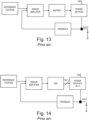
- Figure 13 shows an example of a conventional analog LDO.
- An input voltage V IN is provided to a power device that then produces a corresponding output voltage V OUT .
- a feedback regulation path is established.
- the feedback signal (an analog signal) is provided to an error amplifier, wherein the error with respect to a reference voltage is amplified.
- the analog error amplified signal is fed, via a buffer, back to the power device. Thereby, the output voltage is regulated.
- Figure 14 shows an example of a conventional digital LDO.
- the analog error amplified signal is converted by an analog-to-digital converter (ADC) to a digital signal.
- ADC analog-to-digital converter
- Figure 15 shows an alternative example of a conventional digital LDO, wherein an ADC and a shift register are applied instead of the error amplifier and ADC as in Fig. 14 .
- Figure 16 shows a further alternative example of a conventional digital LDO, wherein an comparator and a so-called coarse class D device are applied instead of the error amplifier and ADC as in Fig. 14 .
- An analog regulator may for example have at least some of the following drawbacks: it needs a complex stability analysis because pole and zero location vary according the load current, requires area due to the power stage in the saturation region, is only suitable for applications requiring high PSRR or for low noise application, portability and scalability for small digital process are complex as conventional architectures are not necessarily convenient for low voltage application.
- a digital regulator may for example have at least some of the following drawbacks: a high ripple, use of ADC and DAC, may require shift register and several comparators to control the power stage, and, due to the shift register, a poor bandwidth and ripple, no operation at a constant frequency.
- a class D LDO may for example have at least some of the following drawbacks: uses a ramp, is process dependent, uses the power device in saturation region, and requires a filtering for the PWM signal to control the power stage.
- a voltage regulator device and a method of operating a voltage regulator device according to the independent claims are described in the following. Exemplary embodiments are described by the dependent claims.
- a voltage regulator device comprising:
- the digital modulation device (e.g. implemented as a delta-sigma modulator) comprises:
- the method further comprises: v) feeding forward the compared feedback signal via a feedforward path beyond the delta-sigma.
- a pulse density modulation (PDM) device which comprises a feedforward path around a delta-sigma, in between a comparator device and a power device of a low dropout voltage regulator.
- PDM pulse density modulation
- a "power device” can in particular comprise a plurality of power units, e.g. a (digital-to-analog) converter and/or a power switch (preferably connected in parallel).
- the power device comprises a plurality of power switches in linear region.
- a power device can be a power stage or a part of a power stage.
- a power stage comprises the power device (in particular with a plurality of power units) and one or more driver device(s) or one or more driver and level shifter device(s).
- a “comparator device” may be a device that is configured to compare two signals, e.g. a feedback signal and a reference signal.
- a comparator may be an error amplifier and may be implemented, for example, as a differential amplifier. In this context, the comparator output can be termed "compared feedback signal”.
- a "digital modulation device” may be a device configured to perform a digital modulation of an (analog) input signal (e.g. a comparator output) to yield a digitally modulated output signal (e.g. to a power device).
- the described digital modulation device can be implemented as a delta-sigma modulator.
- the digital modulation device is realized as a pulse density modulation (PDM) device.
- PDM pulse density modulation
- a “delta-sigma modulator” may be a device that comprises a delta-sigma (unit) (i.e. a difference and an integrator) and a quantizer (unit).
- the quantizer may be, e.g., a single-bit quantizer or a multi-bit quantizer.
- a delta-sigma modulation may convert an analog voltage signal into a pulse width, or pulse density, which can be understood as pulse-density modulation (PDM).
- PDM pulse-density modulation
- the delta-sigma modulator can comprise a feedforward path, e.g. from the input to the quantizer of the delta-sigma modulator.
- the input to the loop filter of the delta-sigma may no longer contain the signal, rather only the filtered quantization noise.
- the loop filter/delta-sigma does not process the signal but only the (shaped) quantized noise.
- the linearity may thus not need not to be high, and the feedforward path may enhance stability and improve the dynamic range.
- the advantage of the feedforward path may be that the loop filter/delta-sigma processes only the quantized noise, by reducing the constraint on the loop filter in terms of dynamic range.
- the present disclosure may be based on the idea that a voltage regulator can operate in an efficient and reliable manner, when the feedback signal from the power device is guided to a comparator device and, via a digital modulation device, back to the power device, wherein the digital modulation device is implemented as a delta-sigma modulator with a delta-sigma, a quantizer, and a feedforward path which feeds forward the comparator output around the delta-sigma.
- the digital modulation device (in particular a PDM controller) controls the regulation loop, meaning that the delta-sigma and the (multi-bit) quantizer control the output power devices. Due to the delta-sigma, the data stream (quantizer) output may be at a fixed sampling rate.
- the described design is a digital one (the control part is fully digital and can be synthetized), so that drawbacks of analog systems are overcome in the first place (operation at lower voltages is enabled compared to analog regulators, since analog design is reduced to a comparator).
- the described device may allow to drive high load current (e.g. 200 mA) with a simplified stability compared to an analog regulator.
- the described voltage regulator may be applied for example to supply circuits such as CPUs, digital functionalities (in particular NFC and secure element products), or memories, as there is no specific constraint in terms of noise or power supply rejected ratio.
- Scalability and portability for digital technology e.g. a node like 16 nm, 28 nm, or 40 nm
- the digital modulation device comprises a pulse density modulation (PDM) device.
- PDM is a form of modulation used to represent an analog signal with a binary signal, wherein the relative density of the pulses essentially corresponds to the amplitude of the analog signal.
- PWM pulse-width modulation
- the described device may operate using the PDM device/controller to control the regulation loop.
- the PDM modulation is achieved through the delta-sigma modulator, the quantizer and the feedforward path. By using the delta-sigma modulator and the quantizer, the output power devices are controlled.
- the quantizer is a multi-bit quantizer (see e.g. Figure 9 below).
- the multi-bit quantizer may allow to control a plurality of power units in a power device/stage at the same time. Thereby, the output voltage ripple may be reduced.
- the data stream (quantizer output) goes through a number of selected power units (and an output capacitor).
- the number of active power units depends on the data stream of the multi-bit quantizer.
- the power device may operate here as a DAC.
- the output voltage ripple may be adjusted through at least one of the following parameters: the number of bits of the multi-bit quantizer, the number of power units in parallel, the switching frequency, the output capacitor properties, the quantization step size, the number of levels of the quantizer.
- the digital modulation device further comprises a digital modulation feedback path, configured to feed back the output of the quantizer to the input of the delta-sigma modulator.
- a digital modulation feedback path configured to feed back the output of the quantizer to the input of the delta-sigma modulator.
- an efficient regulation may be enabled.
- the computation is achieved digitally.
- the respective values of the bits are taken, the bits ⁇ N:1> are included, and a computation with a sum is made. Then, it is amplified through gain Gb and returned to the minus input of the delta domain.
- the digital modulation feedback path can comprise a digital-to-analog converter (DAC) and/or a DAC functionality that is implemented in the computation.
- DAC digital-to-analog converter
- the feedforward path is configured to feedforward the compared feedback signal (comparator output) to a coupling point (sum formation) between the delta-sigma and the quantizer.
- the feedforward path is then added to quantify only the noise in the delta-sigma. Using the feedforward path, one may get only the quantization noise in the delta-sigma.
- the voltage regulator device further comprises a driver device, in particular a driver device and a level shifter device, arranged between the digital modulation device and the power device (and form part of the power stage) and/or between the comparator device and the digital modulation device.
- a driver device in particular a driver device and a level shifter device, arranged between the digital modulation device and the power device (and form part of the power stage) and/or between the comparator device and the digital modulation device.
- the feedforward path is configured to feedforward the compared feedback signal to the driver and/or level shifter device.
- the comparator device (and the power device (and the driver device, in particular the driver device and the level shifter device)) is/are part of an analog domain, and the digital modulation device is part of a digital domain.
- a driver device can be used to set the strength of the signal to control the power device.
- a level shifter device may allow to move from a supply voltage (e.g. high/low) to another one.
- the voltage regulator device is configured as a low dropout (LDO) voltage regulator device.
- LDO low dropout
- the comparator device is configured to compare the feedback signal with a reference voltage to produce the compared feedback signal.
- the comparator may be implemented in continuous time with a hysteresis.
- the voltage regulator device further comprises a clock device, configured to provide a clock signal to the digital modulation device.
- a fast clock e.g. 20 MHz
- a fast clock e.g. 20 MHz
- the clock device is further configured to provide a further clock signal to the comparator device.
- the comparator can be implemented as a latch comparator.
- the power device comprises a plurality of power units such as a power switches.
- the power units can be arranged in linear region (configured as power switches), thereby potentially saving space.
- the power device can be designed with several power units in parallel.
- the plurality of power switches operates as a digital-to analog converter.
- a novel control method for an LDO that combines a comparator with a PDM controller and a power stage.
- the PDM controller is achieved through a digital delta-sigma modulator with a multi-bit quantizer and a feedforward path. This approach reduces complexity in terms of design and stability analysis, saves chip area (as power devices operate only in linear region), improves scalability and portability for digital technology node.
- control method can comprise the following features:
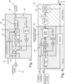
- FIG. 1 illustrates a voltage regulation device 100 according to an exemplary embodiment of the present disclosure.
- the device 100 comprises a power device 150, wherein the power device 150 is configured to receive an input signal 151 (voltage V IN ) and to produce a corresponding output signal 152 (voltage V OUT ).
- a feedback path 140 is coupled to the power device 150 in order to regulate the output signal 152.
- the feedback path 140 guides the output signal 152 as a feedback signal 141 back to a comparator device 110, e.g. an error amplifier.
- the feedback path 140 can comprise a resistor ladder 142.
- the comparator 110 compares the (analog) feedback signal 141 to a reference voltage 115 and produces a corresponding compared feedback signal 112 as an output.
- the comparator output 112 will define, if the output voltage 152 is higher or lower than the target voltage. Said compared feedback signal 112 is then further provided to a digital modulation device 120 that is arranged between the comparator device 110 and the power device 150, thereby closing the feedback/regulation loop.
- the digital modulation device 120 is implemented as a pulse density modulation (PDM) device and configured to digitally modulate the compared feedback signal 112 and to provide the digitally modulated signal 121 back to the power device 150.
- PDM pulse density modulation
- FIG. 2 illustrates a voltage regulation device 100 according to an exemplary embodiment of the present disclosure.
- the device 100 is very similar to the one shown in Figure 1 but shows more details.
- the PDM device 120 is implemented as a delta-sigma modulator that comprises a delta-sigma 122 and a multi-bit quantizer 124.
- a clock device 160 provides a clock signal 161 to the PDM device 120 for the digital modulation.
- a driver (and optionally a level shifter) device 155 Between the PDM device 120 and the power device 150, there is coupled a driver (and optionally a level shifter) device 155.
- the power device 150 (which can comprise a plurality of power units) and the driver/level shifter device 155 form a power stage 156.
- the output 152 further comprises an output capacitor 154 that can be internal or external to the device 100.
- FIG. 3 illustrates the digital modulation device 120 according to an exemplary embodiment of the present disclosure in detail.
- the (analog) compared feedback signal 112 from the comparator device 110 is the input, while the digitally modulated signal 121 (data stream) is the output to the power device 150.
- the delta-sigma 122 comprises a delta domain 122a (difference) and a sigma domain 122b (integrator).
- the feedforward path 128 feeds forward the compared feedback signal 112 to the coupling point 125 (sum) between delta-sigma 122 and quantizer 124.
- the feedforward path 128 can comprise a gain Gc.
- the digital modulation device 120 comprises a feedback path 126 that is established between the output of the quantizer 124 and the coupling point 123 (difference) of the delta domain 122a, the sigma domain 122b, and the comparator output 121.
- the feedback path 126 can further comprise a gain Gb, which is the gain of the delta sigma feedback loop.
- the feedback path 126 is a digital path, and computes the digital quantizer output 121 to a digital value used as negative input of the delta sigma. It can be considered by analogy, that the feedback path functionality is similar to digital-analog converter (DAC) functionality.
- N 8-bit bus
- b1 ⁇ 0000 1111
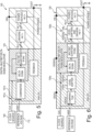
- Figure 4 illustrates a voltage regulation device 100 according to a further exemplary embodiment of the present disclosure.
- Figure 4 shows in principle the detail view of the digital modulation device 120 of Figure 3 in the device of Figure 2 .
- Figure 5 illustrates a voltage regulation device 100 according to a further exemplary embodiment of the present disclosure.
- the clock device 160 is further connected to the comparator device 110 and provides the clock signal 161 thereto.
- the comparator device 110 can be operated as a latch comparator.
- Figure 6 illustrates a voltage regulation device 100 according to a further exemplary embodiment of the present disclosure.
- a first level shifter device 155a coupled between the comparator device 110 and the digital modulation device 120
- a second driver and level shifter device 155b is coupled between the digital modulation device 120 and the power device 150.
- potentially different power domains may be established in the device 100.
- Figure 7 illustrates a voltage regulation device 100 according to a further exemplary embodiment of the present disclosure.
- the feedforward path 128 is configured to feedforward the compared feedback signal 112 to the (second) driver and level shifter device 155b.
- the forward path 128 goes outside the modulator 120 to control directly the power stage 156 (and/or power device 150).
- Figure 8 illustrates alternative representations of the integrator 122b for transfer function computation in Laplace domain or in Z-domain. While in the example on the left side an integrator 122b is applied (see also the previous Figures), the example in the middle applies a Laplace transform/domain for continuous time modelisation. Further, the example on the right side applies a Z-transform/domain for discrete time modelisation.
- Figure 9 illustrates in detail the multi-bit quantizer 124 according to an exemplary embodiment of the present disclosure.
- the digital modulation device 120 is configured as described above, but, in this detailed Figure, it can be seen that the multi-bit quantizer 124 applies a plurality of stages in order to provide the quantizer output(s) 121.
- FIG. 10 illustrates in detail the power device 150 according to an exemplary embodiment of the present disclosure.
- the power device 150 comprises a plurality of power units 158 that are configured as power switches connected in parallel.
- each quantizer output 121 is connected to a specific power switch 158.
- Figure 11 illustrates in a diagram a simulation of the output signal 152 in comparison to a DC load current 153 provided to the power device 150 according to an exemplary embodiment of the present disclosure. Even though the DC load current 153 increases significantly in a linear manner, the voltage output 152 is regulated in an efficient and reliable manner by the described voltage regulator device 100.
- Figure 12 illustrates a digital modulation device 120, here a delta-sigma modulator, according to an exemplary embodiment of the present disclosure.
- This Figure is used as a base for the following calculations regarding the transfer function.
- Ti is the period of the clock (comparable to the sampling period of the integrator).
- An assumption is that the power stage is considered as having a transfer function like a low pass filter.
- V out s H LPF s . y s
- V FB s d .
- V FB s / V REF s a . d . c / T LPF . s + 1 / c . Ti / s + b / Ti . s + 1 / T LPF
- V FB s / N s d / T LPF . ( s / s + b / Ti . 1 / ( s + 1 / T LPF , wherein [s/(s + (b/Ti))] represents a high pass filter.
Landscapes
- Engineering & Computer Science (AREA)
- Physics & Mathematics (AREA)
- Electromagnetism (AREA)
- General Physics & Mathematics (AREA)
- Radar, Positioning & Navigation (AREA)
- Automation & Control Theory (AREA)
- Theoretical Computer Science (AREA)
- Compression, Expansion, Code Conversion, And Decoders (AREA)
Abstract
i) a power device (150), configured to receive an input signal (151) and to produce a corresponding output signal (152);
ii) a comparator device (110), coupled via a feedback path (140) to the power device (150), and configured to receive the output signal (152) as a feedback signal (141), and to produce a compared feedback signal (112); and
iii) a digital modulation device (120), arranged between the comparator device (110) and the power device (150), and configured to digitally modulate the compared feedback signal (112), and to provide the digitally modulated signal (121) to the power device (150), wherein the digital modulation device (120) comprises:
iiia) a delta-sigma (122),
iiib) a quantizer (124), and
iiic) a feedforward path (128), configured to feedforward the compared feedback signal (112) beyond the delta-sigma (122).
Description
- The present disclosure relates to a voltage regulation device that comprises a digital modulation device with a delta-sigma, a quantizer, and a feedforward path. Further, the present disclosure relates to a method of operating the voltage regulation device. Furthermore, the present disclosure related to a specific use of a pulse density modulation device. Thus, the present disclosure may refer to the technical field of voltage regulation.
- Voltage regulators such as LDO (low drop-out) voltage regulators are regulator circuits which are appropriate for many electronic applications, for example in automotive, mobile phone, or industrial applications. The voltage regulators are used to control/regulate a voltage of a power device/stage, thereby providing a well-defined and stable (DC) output voltage.
-
Figure 13 shows an example of a conventional analog LDO. An input voltage VIN is provided to a power device that then produces a corresponding output voltage VOUT. In order to regulate said output voltage, a feedback regulation path is established. The feedback signal (an analog signal) is provided to an error amplifier, wherein the error with respect to a reference voltage is amplified. Then, the analog error amplified signal is fed, via a buffer, back to the power device. Thereby, the output voltage is regulated. -
Figure 14 shows an example of a conventional digital LDO. Instead of the buffer in case of the analog LDO, the analog error amplified signal is converted by an analog-to-digital converter (ADC) to a digital signal. -
Figure 15 shows an alternative example of a conventional digital LDO, wherein an ADC and a shift register are applied instead of the error amplifier and ADC as inFig. 14 . -
Figure 16 shows a further alternative example of a conventional digital LDO, wherein an comparator and a so-called coarse class D device are applied instead of the error amplifier and ADC as inFig. 14 . - However, such conventional LDOs may suffer from different drawbacks. An analog regulator may for example have at least some of the following drawbacks: it needs a complex stability analysis because pole and zero location vary according the load current, requires area due to the power stage in the saturation region, is only suitable for applications requiring high PSRR or for low noise application, portability and scalability for small digital process are complex as conventional architectures are not necessarily convenient for low voltage application.
- A digital regulator may for example have at least some of the following drawbacks: a high ripple, use of ADC and DAC, may require shift register and several comparators to control the power stage, and, due to the shift register, a poor bandwidth and ripple, no operation at a constant frequency.
- A class D LDO may for example have at least some of the following drawbacks: uses a ramp, is process dependent, uses the power device in saturation region, and requires a filtering for the PWM signal to control the power stage.
- In summary, it may be still seen as a challenge to operate a voltage regulator in an efficient and reliable manner.
- There may be a need to operate a voltage regulator in an efficient and reliable manner. A voltage regulator device and a method of operating a voltage regulator device according to the independent claims are described in the following. Exemplary embodiments are described by the dependent claims.
- According to an aspect of the present disclosure, there is described a voltage regulator device, comprising:
- i) a power device, configured to receive an input signal (input voltage) and to produce a corresponding output signal (output voltage);
- ii) a comparator device, coupled via a feedback path to the power device, and configured a) to receive the output signal as a feedback signal, and to b) produce a compared feedback signal (in other words: a comparator output); and
- iii) a digital modulation device, arranged between the comparator device and the power device, and configured
- a) to digitally modulate the compared feedback signal (the comparator output), and b) to provide the digitally modulated signal to the power device.
- The digital modulation device (e.g. implemented as a delta-sigma modulator) comprises:
- iiia) a delta-sigma,
- iiib) a quantizer, and
- iiic) a feedforward path, configured to feedforward the compared feedback signal beyond (around) the delta-sigma (e.g. to a coupling point between the delta-sigma and the quantizer or to the power stage/device, in other words, the feedforward path may feedforward quantified noise from the delta-sigma input beyond the delta-sigma output).
- According to a further aspect of the present disclosure, there is described a method of operating a voltage regulator device, the method comprising:
- i) receiving an input signal and producing a corresponding output signal by a power device;
- ii) receiving the output signal as a feedback signal and producing a compared feedback signal by a comparator device;
- iii) digitally modulating the compared feedback signal (the comparator output) by a digital modulation device that comprises a delta-sigma and a quantizer (arranged downstream of the delta-sigma) to obtain a digitally modulated signal; and
- iv) providing the digitally modulated signal to the power device.
- The method further comprises:
v) feeding forward the compared feedback signal via a feedforward path beyond the delta-sigma. - According to a further aspect of the present disclosure, there is described a use (method of using) of a pulse density modulation (PDM) device, which comprises a feedforward path around a delta-sigma, in between a comparator device and a power device of a low dropout voltage regulator.
- In the context of this document, a "power device" can in particular comprise a plurality of power units, e.g. a (digital-to-analog) converter and/or a power switch (preferably connected in parallel). In an example, the power device comprises a plurality of power switches in linear region. A power device can be a power stage or a part of a power stage. In an example, a power stage comprises the power device (in particular with a plurality of power units) and one or more driver device(s) or one or more driver and level shifter device(s).
- In the context of this document, a "comparator device" may be a device that is configured to compare two signals, e.g. a feedback signal and a reference signal. A comparator may be an error amplifier and may be implemented, for example, as a differential amplifier. In this context, the comparator output can be termed "compared feedback signal".
- In the context of this document, a "digital modulation device" may be a device configured to perform a digital modulation of an (analog) input signal (e.g. a comparator output) to yield a digitally modulated output signal (e.g. to a power device). The described digital modulation device can be implemented as a delta-sigma modulator. In an embodiment, the digital modulation device is realized as a pulse density modulation (PDM) device.
- In the context of this document, a "delta-sigma modulator" may be a device that comprises a delta-sigma (unit) (i.e. a difference and an integrator) and a quantizer (unit). The quantizer may be, e.g., a single-bit quantizer or a multi-bit quantizer. A delta-sigma modulation may convert an analog voltage signal into a pulse width, or pulse density, which can be understood as pulse-density modulation (PDM).
- Further, the delta-sigma modulator can comprise a feedforward path, e.g. from the input to the quantizer of the delta-sigma modulator. The input to the loop filter of the delta-sigma may no longer contain the signal, rather only the filtered quantization noise. Hence, the loop filter/delta-sigma does not process the signal but only the (shaped) quantized noise. The linearity may thus not need not to be high, and the feedforward path may enhance stability and improve the dynamic range. The advantage of the feedforward path may be that the loop filter/delta-sigma processes only the quantized noise, by reducing the constraint on the loop filter in terms of dynamic range.
- According to an exemplary embodiment, the present disclosure may be based on the idea that a voltage regulator can operate in an efficient and reliable manner, when the feedback signal from the power device is guided to a comparator device and, via a digital modulation device, back to the power device, wherein the digital modulation device is implemented as a delta-sigma modulator with a delta-sigma, a quantizer, and a feedforward path which feeds forward the comparator output around the delta-sigma. The digital modulation device (in particular a PDM controller) controls the regulation loop, meaning that the delta-sigma and the (multi-bit) quantizer control the output power devices. Due to the delta-sigma, the data stream (quantizer) output may be at a fixed sampling rate.
- It has been found surprisingly by the inventors that especially the novel feedforward path around the delta sigma may reduce the quantizer noise and thereby improve the output ripple and the device stability. Further, an operation at a constant frequency may be enabled in this manner.
- By these measures, the design is significantly simplified, while the stability analysis complexity is reduced. The described design is a digital one (the control part is fully digital and can be synthetized), so that drawbacks of analog systems are overcome in the first place (operation at lower voltages is enabled compared to analog regulators, since analog design is reduced to a comparator). The described device may allow to drive high load current (e.g. 200 mA) with a simplified stability compared to an analog regulator.
- The described voltage regulator may be applied for example to supply circuits such as CPUs, digital functionalities (in particular NFC and secure element products), or memories, as there is no specific constraint in terms of noise or power supply rejected ratio. Scalability and portability for digital technology (e.g. a node like 16 nm, 28 nm, or 40 nm) can be further improved, which may be important, since digital technology can be demanding regarding maximum power consumption (e.g. 150 mA for an 40 nm product and 230 mA for a 28 nm product).
- In the following, further exemplary embodiments of the device and the method will be explained.
- In an embodiment of the present disclosure, the digital modulation device comprises a pulse density modulation (PDM) device. PDM is a form of modulation used to represent an analog signal with a binary signal, wherein the relative density of the pulses essentially corresponds to the amplitude of the analog signal. Hereby, pulse-width modulation (PWM) may be a special case of PDM, wherein the switching frequency is fixed and all the pulses corresponding to one sample are contiguous in the digital signal. The described device may operate using the PDM device/controller to control the regulation loop. The PDM modulation is achieved through the delta-sigma modulator, the quantizer and the feedforward path. By using the delta-sigma modulator and the quantizer, the output power devices are controlled.
- In a further embodiment of the present disclosure, the quantizer is a multi-bit quantizer (see e.g.
Figure 9 below). The multi-bit quantizer may allow to control a plurality of power units in a power device/stage at the same time. Thereby, the output voltage ripple may be reduced. In an example, the data stream (quantizer output) goes through a number of selected power units (and an output capacitor). Hereby, the number of active power units depends on the data stream of the multi-bit quantizer. The power device may operate here as a DAC. - In an example, the output voltage ripple may be adjusted through at least one of the following parameters: the number of bits of the multi-bit quantizer, the number of power units in parallel, the switching frequency, the output capacitor properties, the quantization step size, the number of levels of the quantizer.
- In a further embodiment of the present disclosure, the digital modulation device further comprises a digital modulation feedback path, configured to feed back the output of the quantizer to the input of the delta-sigma modulator. Thereby, an efficient regulation may be enabled. In an example, the computation is achieved digitally. In an example, the respective values of the bits are taken, the bits <N:1> are included, and a computation with a sum is made. Then, it is amplified through gain Gb and returned to the minus input of the delta domain. The digital modulation feedback path can comprise a digital-to-analog converter (DAC) and/or a DAC functionality that is implemented in the computation.
- In a further embodiment of the present disclosure, the feedforward path is configured to feedforward the compared feedback signal (comparator output) to a coupling point (sum formation) between the delta-sigma and the quantizer. Thereby, only the quantized (filtered, shaped) noise is processed in the loop filter (delta-sigma), thereby improving linearity and dynamic range requirements and stability. The gain of the feedforward path is then added to quantify only the noise in the delta-sigma. Using the feedforward path, one may get only the quantization noise in the delta-sigma.
- In a further embodiment of the present disclosure, the voltage regulator device further comprises a driver device, in particular a driver device and a level shifter device, arranged between the digital modulation device and the power device (and form part of the power stage) and/or between the comparator device and the digital modulation device.
- In a further embodiment of the present disclosure, the feedforward path is configured to feedforward the compared feedback signal to the driver and/or level shifter device.
- In a further embodiment of the present disclosure, the comparator device (and the power device (and the driver device, in particular the driver device and the level shifter device)) is/are part of an analog domain, and the digital modulation device is part of a digital domain. A driver device can be used to set the strength of the signal to control the power device. A level shifter device may allow to move from a supply voltage (e.g. high/low) to another one.
- In a further embodiment of the present disclosure, the voltage regulator device is configured as a low dropout (LDO) voltage regulator device.
- In a further embodiment of the present disclosure, the comparator device is configured to compare the feedback signal with a reference voltage to produce the compared feedback signal. In an example, the comparator may be implemented in continuous time with a hysteresis.
- In a further embodiment of the present disclosure, the voltage regulator device further comprises a clock device, configured to provide a clock signal to the digital modulation device. In an example, a fast clock (e.g. 20 MHz) may be applied.
- In a further embodiment of the present disclosure, the clock device is further configured to provide a further clock signal to the comparator device. In this manner, the comparator can be implemented as a latch comparator.
- In a further embodiment of the present disclosure, the power device comprises a plurality of power units such as a power switches. The power units can be arranged in linear region (configured as power switches), thereby potentially saving space. The power device can be designed with several power units in parallel. In an example, in terms of functionality, the plurality of power switches operates as a digital-to analog converter.
-
-
Figure 1 illustrates a voltage regulation device according to an exemplary embodiment of the present disclosure. -
Figure 2 illustrates a voltage regulation device according to a further exemplary embodiment of the present disclosure. -
Figure 3 illustrates a digital modulation device according to a further exemplary embodiment of the present disclosure. -
Figures 4 to 7 illustrate respectively a voltage regulation device according to further exemplary embodiments of the present disclosure. -
Figure 8 illustrates alternative representations of the integrator for transfer function computation in Laplace domain or in Z-domain. -
Figure 9 illustrates in detail the multi-bit quantizer according to an exemplary embodiment of the present disclosure. -
Figure 10 illustrates in detail the power device according to an exemplary embodiment of the present disclosure. -
Figure 11 illustrates in a diagram a simulation of the output signal in comparison to a load current according to an exemplary embodiment of the present disclosure. -
Figure 12 illustrates a digital modulation device, used to perform calculations regarding the transfer function, according to an exemplary embodiment of the present disclosure. -
Figures 13 to 16 illustrate conventional LDOs (see description above). - The illustrations in the drawings are schematic. In different drawings, similar or identical elements are provided with the same reference signs.
- Before referring to the drawings, exemplary embodiments will be described in further detail, some basic considerations will be summarized based on which exemplary embodiments of the present disclosure have been developed.
- According to exemplary embodiments of the present disclosure, there is described a novel control method for an LDO that combines a comparator with a PDM controller and a power stage. The PDM controller is achieved through a digital delta-sigma modulator with a multi-bit quantizer and a feedforward path. This approach reduces complexity in terms of design and stability analysis, saves chip area (as power devices operate only in linear region), improves scalability and portability for digital technology node.
- According to exemplary embodiments of the present disclosure, the control method can comprise the following features:
- i) decrease design and stability analysis complexity.
- ii) improve scalability and portability for digital technology node.
- iii) PDM controller is achieved through a delta-sigma and a multibit quantizer.
- iv) use a feedforward path in the delta-sigma modulation to reduce the quantization noise and consequently the ripple and also to improve stability.
- v) save area by using the power stage devices in linear region (as switches) and not in saturation as for analog or class D LDO.
- vi) do not have stability issue like internal pole and zero variations due to large current load variation.
- vii) has a reduced number of poles and zeros compared to an analog solution.
- viii) does not require error amplifier with stability, buffer, pole tracking or power device in saturation.
- ix) can operate at lower voltage compared to analog regulator, as only a comparator and power switches are required in the analog part.
- x) the control part is fully digital and can be synthetized.
-
Figure 1 illustrates avoltage regulation device 100 according to an exemplary embodiment of the present disclosure. Thedevice 100 comprises apower device 150, wherein thepower device 150 is configured to receive an input signal 151 (voltage VIN) and to produce a corresponding output signal 152 (voltage VOUT). Afeedback path 140 is coupled to thepower device 150 in order to regulate theoutput signal 152. Thefeedback path 140 guides theoutput signal 152 as afeedback signal 141 back to acomparator device 110, e.g. an error amplifier. Thefeedback path 140 can comprise aresistor ladder 142. Thecomparator 110 compares the (analog)feedback signal 141 to areference voltage 115 and produces a corresponding comparedfeedback signal 112 as an output. Thecomparator output 112 will define, if theoutput voltage 152 is higher or lower than the target voltage. Said comparedfeedback signal 112 is then further provided to adigital modulation device 120 that is arranged between thecomparator device 110 and thepower device 150, thereby closing the feedback/regulation loop. Thedigital modulation device 120 is implemented as a pulse density modulation (PDM) device and configured to digitally modulate the comparedfeedback signal 112 and to provide the digitally modulatedsignal 121 back to thepower device 150. -
Figure 2 illustrates avoltage regulation device 100 according to an exemplary embodiment of the present disclosure. Thedevice 100 is very similar to the one shown inFigure 1 but shows more details. It can be seen that thePDM device 120 is implemented as a delta-sigma modulator that comprises a delta-sigma 122 and amulti-bit quantizer 124. Aclock device 160 provides aclock signal 161 to thePDM device 120 for the digital modulation. Between thePDM device 120 and thepower device 150, there is coupled a driver (and optionally a level shifter)device 155. The power device 150 (which can comprise a plurality of power units) and the driver/level shifter device 155 form apower stage 156. Further, it is illustrated that thecomparator device 110, the feedback path 140 (in principle also the power device 150) and the driver/level-shifter devices 155 form an analog (signal) domain, while thePDM 120 forms a digital (signal) domain. Theoutput 152 further comprises anoutput capacitor 154 that can be internal or external to thedevice 100. -
Figure 3 illustrates thedigital modulation device 120 according to an exemplary embodiment of the present disclosure in detail. The (analog) compared feedback signal 112 from thecomparator device 110 is the input, while the digitally modulated signal 121 (data stream) is the output to thepower device 150. The delta-sigma 122 comprises adelta domain 122a (difference) and asigma domain 122b (integrator). There is established afeedforward path 128, configured to feedforward the comparedfeedback signal 112 beyond (around) the delta-sigma 122. In particular, in this example, thefeedforward path 128 feeds forward the comparedfeedback signal 112 to the coupling point 125 (sum) between delta-sigma 122 andquantizer 124. Thefeedforward path 128 can comprise a gain Gc. - Further, the
digital modulation device 120 comprises afeedback path 126 that is established between the output of thequantizer 124 and the coupling point 123 (difference) of thedelta domain 122a, thesigma domain 122b, and thecomparator output 121. Thefeedback path 126 can further comprise a gain Gb, which is the gain of the delta sigma feedback loop. Thefeedback path 126 is a digital path, and computes thedigital quantizer output 121 to a digital value used as negative input of the delta sigma. It can be considered by analogy, that the feedback path functionality is similar to digital-analog converter (DAC) functionality. - The signal feedback FB corresponds in this example to the sum of the binary bits on the data stream bus <N:1>, in other words, it follows the following equation:


-
Figure 4 illustrates avoltage regulation device 100 according to a further exemplary embodiment of the present disclosure.Figure 4 shows in principle the detail view of thedigital modulation device 120 ofFigure 3 in the device ofFigure 2 . -
Figure 5 illustrates avoltage regulation device 100 according to a further exemplary embodiment of the present disclosure. In this example, theclock device 160 is further connected to thecomparator device 110 and provides theclock signal 161 thereto. In this manner, thecomparator device 110 can be operated as a latch comparator. -
Figure 6 illustrates avoltage regulation device 100 according to a further exemplary embodiment of the present disclosure. In this example, which is based on the example ofFigure 5 , there is a firstlevel shifter device 155a coupled between thecomparator device 110 and thedigital modulation device 120, while a second driver andlevel shifter device 155b is coupled between thedigital modulation device 120 and thepower device 150. Thereby, potentially different power domains may be established in thedevice 100. -
Figure 7 illustrates avoltage regulation device 100 according to a further exemplary embodiment of the present disclosure. In this example, which is based on the example shown inFigure 4 , thefeedforward path 128 is configured to feedforward the comparedfeedback signal 112 to the (second) driver andlevel shifter device 155b. In this case, theforward path 128 goes outside themodulator 120 to control directly the power stage 156 (and/or power device 150). -
Figure 8 illustrates alternative representations of theintegrator 122b for transfer function computation in Laplace domain or in Z-domain. While in the example on the left side anintegrator 122b is applied (see also the previous Figures), the example in the middle applies a Laplace transform/domain for continuous time modelisation. Further, the example on the right side applies a Z-transform/domain for discrete time modelisation. -
Figure 9 illustrates in detail themulti-bit quantizer 124 according to an exemplary embodiment of the present disclosure. Thedigital modulation device 120 is configured as described above, but, in this detailed Figure, it can be seen that themulti-bit quantizer 124 applies a plurality of stages in order to provide the quantizer output(s) 121. -
Figure 10 illustrates in detail thepower device 150 according to an exemplary embodiment of the present disclosure. In this detailed example, thepower device 150 comprises a plurality ofpower units 158 that are configured as power switches connected in parallel. In this example, eachquantizer output 121 is connected to aspecific power switch 158. -
Figure 11 illustrates in a diagram a simulation of theoutput signal 152 in comparison to a DC load current 153 provided to thepower device 150 according to an exemplary embodiment of the present disclosure. Even though the DC load current 153 increases significantly in a linear manner, thevoltage output 152 is regulated in an efficient and reliable manner by the describedvoltage regulator device 100. -
Figure 12 illustrates adigital modulation device 120, here a delta-sigma modulator, according to an exemplary embodiment of the present disclosure. This Figure is used as a base for the following calculations regarding the transfer function. Hereby, Ti is the period of the clock (comparable to the sampling period of the integrator). An assumption is that the power stage is considered as having a transfer function like a low pass filter. - For the following computation, we consider
- a is the comparator gain
- b is the delta sigma modulator feedback gain
- c is the feedforward path gain
- d is the regulator feedback gain
- Vout(s) is the output of the regulator
- Ti is the period of the clock
- VFB(s) is the regulator feedback
- VREF(s) is the reference of the regulator
-


- 1) if N(s) = 0, the open loop signal transfer function is

- The open loop signal transfer function is

- From this transfer function, poles and zeros can be described as follows:




- By having b = 1/c in a computation, the pole and zero of the integrator (of the delta-sigma) cancel each other, thereby simplifying stability as the stability response is similar to a first order stability system. It follows in particular, that by providing the feedforward path (see c) and the feedback path (see b), the stability of the described voltage regulator device can be improved.
- 2) if VREF(s) = 0, the open loop noise transfer function is

- The open loop noise transfer function is

-
- 100
- Voltage regulation device
- 110
- Comparator device
- 112
- Compared feedback signal, comparator output
- 115
- Reference signal/voltage
- 120
- Digital modulation device
- 121
- Quantizer output, data stream
- 122
- Delta-sigma
- 122a
- Delta domain
- 122b
- Sigma domain, integrator
- 123
- First coupling point (difference)
- 124
- Quantizer
- 125
- Second coupling point (sum)
- 126
- Digital modulation feedback path
- 128
- Feedforward path
- 140
- Feedback path
- 141
- Feedback signal
- 142
- Resistor ladder or unity gain feedback path
- 150
- Power device
- 151
- Input signal/voltage
- 152
- Output signal/voltage
- 153
- DC load current
- 154
- Output capacitor
- 155
- Driver device
- 155a
- Level-shifter device
- 155b
- Driver and level-shifter device
- 156
- Power stage
- 158
- Power unit, power switch
- 160
- Clock device
- 161, 161a,b
- Clock signal
Claims (15)
- A voltage regulator device (100), comprising:a power device (150), configured to receive an input signal (151) and to produce a corresponding output signal (152);a comparator device (110), coupled via a feedback path (140) to the power device (150), and configured toreceive the output signal (152) as a feedback signal (141), andproduce a compared feedback signal (112); anda digital modulation device (120), arranged between the comparator device (110) and the power device (150), and configured todigitally modulate the compared feedback signal (112), andprovide the digitally modulated signal (121) to the power device (150),wherein the digital modulation device (120) comprises:a delta-sigma (122),a quantizer (124), anda feedforward path (128), configured to feedforward the compared feedback signal (112) beyond the delta-sigma (122).
- The voltage regulator device (100) according to claim 1,
wherein the digital modulation device (120) comprises a pulse density modulation, PDM, device. - The voltage regulator device (100) according to claim 1 or 2,
wherein the quantizer (124) is a multi-bit quantizer. - The voltage regulator device (100) according to any one of the preceding claims, wherein the digital modulation device (120) further comprises:
a digital modulation feedback path (126), configured to feed-back the output of the quantizer (124) to the delta-sigma (122). - The voltage regulator device (100) according to any one of the preceding claims,
wherein the feedforward path (128) is configured to feedforward the compared feedback signal (112) to a coupling (125) between the delta-sigma (122) and the quantizer (124). - The voltage regulator device (100) according to any one of the preceding claims, further comprising at least one of the following features:a driver device (155) arranged between the digital modulation device (120) and the power device (150);a driver device and a level shifter device (155) arranged between the digital modulation device (120) and the power device (150);a level shifter (155a) between the comparator device (110) and the digital modulation device (120).
- The voltage regulator device (100) according to claim 6,
wherein the feedforward path (128) is configured to feedforward the compared feedback signal (112) to the driver device (155) or to the driver device and the level shifter device (155). - The voltage regulator device (100) according to any one of the preceding claims, wherein the comparator device (110) is part of an analog domain, and
wherein the digital modulation device (120) is part of a digital domain. - The voltage regulator device (100) according to any one of the preceding claims, wherein the voltage regulator device (100) is configured as a low dropout, LDO, device.
- The voltage regulator device (100) according to any one of the preceding claims, wherein the comparator device (110) is configured to compare the feedback signal (141) with a reference voltage (115) to produce the compared feedback signal (112).
- The voltage regulator device (100) according to any one of the preceding claims, further comprising:
a clock device (160), configured to provide a clock signal (161a) to the digital modulation device (120). - The voltage regulator device (100) according to claim 11,
wherein the clock device (160) is further configured to provide a further clock signal (161b) to the comparator device (110). - The voltage regulator device (100) according to any one of the preceding claims, wherein the power device (150) comprises a plurality of power units (158) configured as power switches.
- A method of operating a voltage regulator device (100), comprising:receiving an input signal (151) and producing a corresponding output signal (152) by a power device (150);receiving the output signal (152) as a feedback signal (141) and producing a compared feedback signal (112) by a comparator device (110);digitally modulating the compared feedback signal (112) by a digital modulation device (120) that comprises a delta-sigma (122) and a quantizer (124) to obtain a digitally modulated signal (121);providing the digitally modulated signal (121) to the power device (150);wherein the method further comprises:
feeding forward the compared feedback signal (112) via a feedforward path (128) beyond the delta-sigma (122). - Using a delta-sigma modulator (120), which comprises a feedforward path (128) around the delta-sigma part (122), in between a comparator device (110) and a power device (150) of a low dropout voltage regulator (100).
Priority Applications (3)
| Application Number | Priority Date | Filing Date | Title |
|---|---|---|---|
| EP21306831.5A EP4198676A1 (en) | 2021-12-17 | 2021-12-17 | Voltage regulation using a delta-sigma modulator, device and method |
| US18/048,163 US12366874B2 (en) | 2021-12-17 | 2022-10-20 | Voltage regulation using a delta-sigma modulator, device and method |
| CN202211394907.1A CN116266063A (en) | 2021-12-17 | 2022-11-08 | Voltage regulation apparatus and method using delta-sigma modulator |
Applications Claiming Priority (1)
| Application Number | Priority Date | Filing Date | Title |
|---|---|---|---|
| EP21306831.5A EP4198676A1 (en) | 2021-12-17 | 2021-12-17 | Voltage regulation using a delta-sigma modulator, device and method |
Publications (1)
| Publication Number | Publication Date |
|---|---|
| EP4198676A1 true EP4198676A1 (en) | 2023-06-21 |
Family
ID=79601465
Family Applications (1)
| Application Number | Title | Priority Date | Filing Date |
|---|---|---|---|
| EP21306831.5A Pending EP4198676A1 (en) | 2021-12-17 | 2021-12-17 | Voltage regulation using a delta-sigma modulator, device and method |
Country Status (3)
| Country | Link |
|---|---|
| US (1) | US12366874B2 (en) |
| EP (1) | EP4198676A1 (en) |
| CN (1) | CN116266063A (en) |
Families Citing this family (2)
| Publication number | Priority date | Publication date | Assignee | Title |
|---|---|---|---|---|
| US12326748B2 (en) * | 2022-02-10 | 2025-06-10 | Nxp B.V. | Linear voltage regulator using serial bit stream for voltage regulation |
| US20250216879A1 (en) * | 2024-01-02 | 2025-07-03 | Taiwan Semiconductor Manufacturing Company, Ltd. | DLVR System with Duty Cycle Timing Control |
Citations (3)
| Publication number | Priority date | Publication date | Assignee | Title |
|---|---|---|---|---|
| US20060261789A1 (en) * | 2005-05-17 | 2006-11-23 | May Marcus W | Method and apparatus for digitally regulating an output voltage using noise-shaped component selection |
| JP2013102638A (en) * | 2011-11-09 | 2013-05-23 | Gunma Univ | Switching power supply circuit |
| US20160202715A1 (en) * | 2015-01-12 | 2016-07-14 | Dmitry Petrov | Low-noise sampled voltage regulator |
Family Cites Families (14)
| Publication number | Priority date | Publication date | Assignee | Title |
|---|---|---|---|---|
| EP1336912A1 (en) | 2002-02-18 | 2003-08-20 | Motorola, Inc. | Low drop-out voltage regulator |
| US8476966B2 (en) * | 2010-10-05 | 2013-07-02 | International Business Machines Corporation | On-die voltage regulation using p-FET header devices with a feedback control loop |
| US8643436B2 (en) * | 2011-11-22 | 2014-02-04 | Analog Devices, Inc. | Multi-level boosted Class D amplifier |
| US8928301B2 (en) * | 2012-06-13 | 2015-01-06 | Atmel Corporation | Pulse width modulation based controller |
| US9069370B2 (en) | 2012-06-29 | 2015-06-30 | Taiwan Semiconductor Manufacturing Company, Ltd. | Digital low drop-out regulator |
| US8779957B2 (en) * | 2012-08-02 | 2014-07-15 | Qualcomm Incorporated | Low distortion feed-forward delta-sigma modulator |
| US9281745B2 (en) * | 2012-11-01 | 2016-03-08 | Stellamar Llc | Digital controller for switch-mode DC-DC converters and method |
| US9766678B2 (en) | 2013-02-04 | 2017-09-19 | Intel Corporation | Multiple voltage identification (VID) power architecture, a digital synthesizable low dropout regulator, and apparatus for improving reliability of power gates |
| US10698432B2 (en) | 2013-03-13 | 2020-06-30 | Intel Corporation | Dual loop digital low drop regulator and current sharing control apparatus for distributable voltage regulators |
| US20140266103A1 (en) | 2013-03-15 | 2014-09-18 | Qualcomm Incorporated | Digitally assisted regulation for an integrated capless low-dropout (ldo) voltage regulator |
| CN104348489B (en) * | 2013-07-25 | 2019-01-18 | 瑞昱半导体股份有限公司 | Feed-forward type delta-sigma modulator |
| CN104793683B (en) * | 2015-04-20 | 2016-09-14 | 樊晓微 | Mixed stable voltage power supply |
| US10126766B2 (en) | 2016-01-26 | 2018-11-13 | Samsung Electronics Co., Ltd. | Low dropout voltage (LDO) regulator including a dual loop circuit and an application processor and a user device including the same |
| US10126769B2 (en) | 2016-09-12 | 2018-11-13 | Marvell World Trade Ltd. | Class-D driven low-drop-output (LDO) regulator |
-
2021
- 2021-12-17 EP EP21306831.5A patent/EP4198676A1/en active Pending
-
2022
- 2022-10-20 US US18/048,163 patent/US12366874B2/en active Active
- 2022-11-08 CN CN202211394907.1A patent/CN116266063A/en active Pending
Patent Citations (3)
| Publication number | Priority date | Publication date | Assignee | Title |
|---|---|---|---|---|
| US20060261789A1 (en) * | 2005-05-17 | 2006-11-23 | May Marcus W | Method and apparatus for digitally regulating an output voltage using noise-shaped component selection |
| JP2013102638A (en) * | 2011-11-09 | 2013-05-23 | Gunma Univ | Switching power supply circuit |
| US20160202715A1 (en) * | 2015-01-12 | 2016-07-14 | Dmitry Petrov | Low-noise sampled voltage regulator |
Non-Patent Citations (1)
| Title |
|---|
| GHARBIYA A ET AL: "Fully digital feedforward delta-sigma modulator", RESEARCH IN MICROELECTRONICS AND ELECTRONICS, 2005 PHD JULY, 25, 2005, PISCATAWAY, NJ, USA,IEEE, PISCATAWAY, NJ, USA, vol. 1, 25 July 2005 (2005-07-25), pages 97 - 100, XP010858628, ISBN: 978-0-7803-9345-5, DOI: 10.1109/RME.2005.1543013 * |
Also Published As
| Publication number | Publication date |
|---|---|
| CN116266063A (en) | 2023-06-20 |
| US20230195151A1 (en) | 2023-06-22 |
| US12366874B2 (en) | 2025-07-22 |
Similar Documents
| Publication | Publication Date | Title |
|---|---|---|
| US6653960B2 (en) | Stabilized power supply using delta sigma modulator | |
| US9013341B2 (en) | Noise shaping for digital pulse-width modulators | |
| US7449869B2 (en) | Digital current mode controller with low frequency current sampling | |
| US12366874B2 (en) | Voltage regulation using a delta-sigma modulator, device and method | |
| EP2122831B1 (en) | Digital double-loop output voltage regulation | |
| CN1582534B (en) | Variable full-scale multi-bit σ-δ analog-to-digital converter | |
| US7504812B2 (en) | Transient behavior while switching between control loops in a switching voltage regulator | |
| JP2006512851A (en) | Delta-sigma amplifier with output stage supply voltage variation compensation and method and digital amplifier system using the same | |
| JP2007068254A (en) | DC-DC converter control circuit and control method thereof | |
| JP4708159B2 (en) | Digital amplifier | |
| US20080048628A1 (en) | Voltage converter and a method of using the same | |
| KR101236700B1 (en) | Switched capacitor circuit | |
| Rao et al. | Noise-shaping techniques applied to switched-capacitor voltage regulators | |
| US20080024341A1 (en) | Delta sigma modulation d/a converting system | |
| US20250219543A1 (en) | Control circuit and switching power supply thereof | |
| JP2002369503A (en) | Dc-dc converter | |
| KR100219969B1 (en) | 3-Level Digital-to-Analog Converter and How to Convert a Digital Signal to an Analog Signal | |
| US9136805B2 (en) | Class HD power amplifier | |
| Chen et al. | An improved low-EMI fast-transient-response buck converter suitable for wireless sensor networks with new transient accelerated techniques | |
| CN102136799B (en) | Current mode converter with self-calibration output | |
| Yu et al. | Use of sliding-mode modulation in switch-mode power amplification | |
| JP2013102638A (en) | Switching power supply circuit | |
| JP2013009516A (en) | Switching power circuit | |
| US7423566B2 (en) | Sigma-delta modulator using a passive filter | |
| Zhao et al. | Non-zero error method for improving output voltage regulation of low-resolution digital controllers for SMPS |
Legal Events
| Date | Code | Title | Description |
|---|---|---|---|
| PUAI | Public reference made under article 153(3) epc to a published international application that has entered the european phase |
Free format text: ORIGINAL CODE: 0009012 |
|
| STAA | Information on the status of an ep patent application or granted ep patent |
Free format text: STATUS: THE APPLICATION HAS BEEN PUBLISHED |
|
| AK | Designated contracting states |
Kind code of ref document: A1 Designated state(s): AL AT BE BG CH CY CZ DE DK EE ES FI FR GB GR HR HU IE IS IT LI LT LU LV MC MK MT NL NO PL PT RO RS SE SI SK SM TR |
|
| STAA | Information on the status of an ep patent application or granted ep patent |
Free format text: STATUS: REQUEST FOR EXAMINATION WAS MADE |
|
| 17P | Request for examination filed |
Effective date: 20231221 |
|
| RBV | Designated contracting states (corrected) |
Designated state(s): AL AT BE BG CH CY CZ DE DK EE ES FI FR GB GR HR HU IE IS IT LI LT LU LV MC MK MT NL NO PL PT RO RS SE SI SK SM TR |