EP4198026A1 - Compounds for use in semiconductiong materials suitable for electronic devices - Google Patents
Compounds for use in semiconductiong materials suitable for electronic devices Download PDFInfo
- Publication number
- EP4198026A1 EP4198026A1 EP21214412.5A EP21214412A EP4198026A1 EP 4198026 A1 EP4198026 A1 EP 4198026A1 EP 21214412 A EP21214412 A EP 21214412A EP 4198026 A1 EP4198026 A1 EP 4198026A1
- Authority
- EP
- European Patent Office
- Prior art keywords
- aza
- analogs
- substituted
- group
- diyl
- Prior art date
- Legal status (The legal status is an assumption and is not a legal conclusion. Google has not performed a legal analysis and makes no representation as to the accuracy of the status listed.)
- Pending
Links
- 150000001875 compounds Chemical class 0.000 title claims abstract description 107
- 239000000463 material Substances 0.000 title description 28
- 239000004065 semiconductor Substances 0.000 claims abstract description 13
- -1 anthracene-diyl Chemical group 0.000 claims description 84
- 125000001997 phenyl group Chemical group [H]C1=C([H])C([H])=C(*)C([H])=C1[H] 0.000 claims description 56
- 125000001072 heteroaryl group Chemical group 0.000 claims description 55
- 125000003118 aryl group Chemical group 0.000 claims description 49
- JYEUMXHLPRZUAT-UHFFFAOYSA-N 1,2,3-triazine Chemical group C1=CN=NN=C1 JYEUMXHLPRZUAT-UHFFFAOYSA-N 0.000 claims description 23
- 125000001183 hydrocarbyl group Chemical group 0.000 claims description 23
- 125000005331 diazinyl group Chemical group N1=NC(=CC=C1)* 0.000 claims description 20
- 125000004076 pyridyl group Chemical group 0.000 claims description 19
- 125000000732 arylene group Chemical group 0.000 claims description 18
- 125000005549 heteroarylene group Chemical group 0.000 claims description 17
- KYQCOXFCLRTKLS-UHFFFAOYSA-N Pyrazine Chemical compound C1=CN=CC=N1 KYQCOXFCLRTKLS-UHFFFAOYSA-N 0.000 claims description 14
- 125000004432 carbon atom Chemical group C* 0.000 claims description 11
- UFWIBTONFRDIAS-UHFFFAOYSA-N Naphthalene Chemical compound C1=CC=CC2=CC=CC=C21 UFWIBTONFRDIAS-UHFFFAOYSA-N 0.000 claims description 8
- SMWDFEZZVXVKRB-UHFFFAOYSA-N Quinoline Chemical compound N1=CC=CC2=CC=CC=C21 SMWDFEZZVXVKRB-UHFFFAOYSA-N 0.000 claims description 8
- JWVCLYRUEFBMGU-UHFFFAOYSA-N quinazoline Chemical compound N1=CN=CC2=CC=CC=C21 JWVCLYRUEFBMGU-UHFFFAOYSA-N 0.000 claims description 8
- 229910052717 sulfur Inorganic materials 0.000 claims description 8
- PCNDJXKNXGMECE-UHFFFAOYSA-N Phenazine Natural products C1=CC=CC2=NC3=CC=CC=C3N=C21 PCNDJXKNXGMECE-UHFFFAOYSA-N 0.000 claims description 7
- CZPWVGJYEJSRLH-UHFFFAOYSA-N Pyrimidine Chemical compound C1=CN=CN=C1 CZPWVGJYEJSRLH-UHFFFAOYSA-N 0.000 claims description 7
- PQIUGRLKNKSKTC-UHFFFAOYSA-N benzo[h]quinazoline Chemical compound N1=CN=C2C3=CC=CC=C3C=CC2=C1 PQIUGRLKNKSKTC-UHFFFAOYSA-N 0.000 claims description 7
- 229910052760 oxygen Inorganic materials 0.000 claims description 7
- 125000003373 pyrazinyl group Chemical group 0.000 claims description 7
- 125000000714 pyrimidinyl group Chemical group 0.000 claims description 7
- HYZJCKYKOHLVJF-UHFFFAOYSA-N 1H-benzimidazole Chemical compound C1=CC=C2NC=NC2=C1 HYZJCKYKOHLVJF-UHFFFAOYSA-N 0.000 claims description 6
- MWPLVEDNUUSJAV-UHFFFAOYSA-N anthracene Chemical compound C1=CC=CC2=CC3=CC=CC=C3C=C21 MWPLVEDNUUSJAV-UHFFFAOYSA-N 0.000 claims description 6
- IOJUPLGTWVMSFF-UHFFFAOYSA-N benzothiazole Chemical compound C1=CC=C2SC=NC2=C1 IOJUPLGTWVMSFF-UHFFFAOYSA-N 0.000 claims description 6
- YNPNZTXNASCQKK-UHFFFAOYSA-N phenanthrene Chemical compound C1=CC=C2C3=CC=CC=C3C=CC2=C1 YNPNZTXNASCQKK-UHFFFAOYSA-N 0.000 claims description 6
- XSCHRSMBECNVNS-UHFFFAOYSA-N quinoxaline Chemical compound N1=CC=NC2=CC=CC=C21 XSCHRSMBECNVNS-UHFFFAOYSA-N 0.000 claims description 6
- GAMYYCRTACQSBR-UHFFFAOYSA-N 4-azabenzimidazole Chemical compound C1=CC=C2NC=NC2=N1 GAMYYCRTACQSBR-UHFFFAOYSA-N 0.000 claims description 5
- JIHQDMXYYFUGFV-UHFFFAOYSA-N 1,3,5-triazine Chemical compound C1=NC=NC=N1 JIHQDMXYYFUGFV-UHFFFAOYSA-N 0.000 claims description 4
- FCEHBMOGCRZNNI-UHFFFAOYSA-N 1-benzothiophene Chemical compound C1=CC=C2SC=CC2=C1 FCEHBMOGCRZNNI-UHFFFAOYSA-N 0.000 claims description 4
- IYYZUPMFVPLQIF-UHFFFAOYSA-N dibenzothiophene Chemical compound C1=CC=C2C3=CC=CC=C3SC2=C1 IYYZUPMFVPLQIF-UHFFFAOYSA-N 0.000 claims description 4
- 125000005551 pyridylene group Chemical group 0.000 claims description 4
- 125000005576 pyrimidinylene group Chemical group 0.000 claims description 4
- 125000006413 ring segment Chemical group 0.000 claims description 4
- 125000005558 triazinylene group Chemical group 0.000 claims description 4
- 125000005559 triazolylene group Chemical group 0.000 claims description 4
- UYVFEZBIQHCLBF-UHFFFAOYSA-N 3h-imidazo[4,5-f]quinoline Chemical compound C1=CC=C2C(N=CN3)=C3C=CC2=N1 UYVFEZBIQHCLBF-UHFFFAOYSA-N 0.000 claims description 3
- 125000006615 aromatic heterocyclic group Chemical group 0.000 claims description 3
- 125000002837 carbocyclic group Chemical group 0.000 claims description 3
- WCZVZNOTHYJIEI-UHFFFAOYSA-N cinnoline Chemical compound N1=NC=CC2=CC=CC=C21 WCZVZNOTHYJIEI-UHFFFAOYSA-N 0.000 claims description 3
- TXCDCPKCNAJMEE-UHFFFAOYSA-N dibenzofuran Chemical compound C1=CC=C2C3=CC=CC=C3OC2=C1 TXCDCPKCNAJMEE-UHFFFAOYSA-N 0.000 claims description 3
- NIHNNTQXNPWCJQ-UHFFFAOYSA-N fluorene Chemical compound C1=CC=C2CC3=CC=CC=C3C2=C1 NIHNNTQXNPWCJQ-UHFFFAOYSA-N 0.000 claims description 3
- 125000002541 furyl group Chemical group 0.000 claims description 3
- 150000003020 phtalazines Chemical class 0.000 claims description 3
- 125000002098 pyridazinyl group Chemical group 0.000 claims description 3
- 125000001544 thienyl group Chemical group 0.000 claims description 3
- BCMCBBGGLRIHSE-UHFFFAOYSA-N 1,3-benzoxazole Chemical compound C1=CC=C2OC=NC2=C1 BCMCBBGGLRIHSE-UHFFFAOYSA-N 0.000 claims description 2
- IANQTJSKSUMEQM-UHFFFAOYSA-N 1-benzofuran Chemical compound C1=CC=C2OC=CC2=C1 IANQTJSKSUMEQM-UHFFFAOYSA-N 0.000 claims description 2
- HKMTVMBEALTRRR-UHFFFAOYSA-N Benzo[a]fluorene Chemical compound C1=CC=CC2=C3CC4=CC=CC=C4C3=CC=C21 HKMTVMBEALTRRR-UHFFFAOYSA-N 0.000 claims description 2
- XNKVIGSNRYAOQZ-UHFFFAOYSA-N dibenzofluorene Chemical compound C12=CC=CC=C2C2=CC=CC=C2C2=C1CC1=CC=CC=C12 XNKVIGSNRYAOQZ-UHFFFAOYSA-N 0.000 claims description 2
- PBMFSQRYOILNGV-UHFFFAOYSA-N pyridazine Chemical compound C1=CC=NN=C1 PBMFSQRYOILNGV-UHFFFAOYSA-N 0.000 claims description 2
- 125000000843 phenylene group Chemical group C1(=C(C=CC=C1)*)* 0.000 claims 1
- 125000005550 pyrazinylene group Chemical group 0.000 claims 1
- 239000010410 layer Substances 0.000 description 281
- 238000002347 injection Methods 0.000 description 52
- 239000007924 injection Substances 0.000 description 52
- 230000000903 blocking effect Effects 0.000 description 38
- 239000000758 substrate Substances 0.000 description 35
- 239000002019 doping agent Substances 0.000 description 28
- 238000000151 deposition Methods 0.000 description 26
- 230000005525 hole transport Effects 0.000 description 26
- 230000008021 deposition Effects 0.000 description 25
- 239000011159 matrix material Substances 0.000 description 17
- BWHMMNNQKKPAPP-UHFFFAOYSA-L potassium carbonate Chemical compound [K+].[K+].[O-]C([O-])=O BWHMMNNQKKPAPP-UHFFFAOYSA-L 0.000 description 15
- IJGRMHOSHXDMSA-UHFFFAOYSA-N Atomic nitrogen Chemical compound N#N IJGRMHOSHXDMSA-UHFFFAOYSA-N 0.000 description 14
- 229910052751 metal Inorganic materials 0.000 description 13
- 239000002184 metal Substances 0.000 description 13
- VYPSYNLAJGMNEJ-UHFFFAOYSA-N Silicium dioxide Chemical compound O=[Si]=O VYPSYNLAJGMNEJ-UHFFFAOYSA-N 0.000 description 12
- MVPPADPHJFYWMZ-UHFFFAOYSA-N chlorobenzene Chemical compound ClC1=CC=CC=C1 MVPPADPHJFYWMZ-UHFFFAOYSA-N 0.000 description 12
- 238000004770 highest occupied molecular orbital Methods 0.000 description 12
- 239000011777 magnesium Substances 0.000 description 12
- 229910052757 nitrogen Inorganic materials 0.000 description 12
- 125000000217 alkyl group Chemical group 0.000 description 11
- 239000011248 coating agent Substances 0.000 description 11
- 238000000576 coating method Methods 0.000 description 11
- 239000000203 mixture Substances 0.000 description 11
- 238000000859 sublimation Methods 0.000 description 11
- 230000008022 sublimation Effects 0.000 description 11
- 238000004768 lowest unoccupied molecular orbital Methods 0.000 description 10
- OKKJLVBELUTLKV-UHFFFAOYSA-N Methanol Chemical compound OC OKKJLVBELUTLKV-UHFFFAOYSA-N 0.000 description 9
- 238000004528 spin coating Methods 0.000 description 9
- 238000001771 vacuum deposition Methods 0.000 description 9
- XLYOFNOQVPJJNP-UHFFFAOYSA-N water Substances O XLYOFNOQVPJJNP-UHFFFAOYSA-N 0.000 description 9
- GSOFUHOPEHYQGN-UHFFFAOYSA-N C1=CC=C(C2=NC(=NC(=N2)C2=C(Br)C3=CC=CC=C3C=C2)C2=CC=CC=C2)C=C1 Chemical compound C1=CC=C(C2=NC(=NC(=N2)C2=C(Br)C3=CC=CC=C3C=C2)C2=CC=CC=C2)C=C1 GSOFUHOPEHYQGN-UHFFFAOYSA-N 0.000 description 8
- 125000003545 alkoxy group Chemical group 0.000 description 8
- 229910052749 magnesium Inorganic materials 0.000 description 8
- 239000000126 substance Substances 0.000 description 8
- 239000011575 calcium Substances 0.000 description 7
- 125000004051 hexyl group Chemical group [H]C([H])([H])C([H])([H])C([H])([H])C([H])([H])C([H])([H])C([H])([H])* 0.000 description 7
- 238000000034 method Methods 0.000 description 7
- 125000001424 substituent group Chemical group 0.000 description 7
- 229910052769 Ytterbium Inorganic materials 0.000 description 6
- 229910052791 calcium Inorganic materials 0.000 description 6
- 239000003795 chemical substances by application Substances 0.000 description 6
- 239000000306 component Substances 0.000 description 6
- NXQGGXCHGDYOHB-UHFFFAOYSA-L cyclopenta-1,4-dien-1-yl(diphenyl)phosphane;dichloropalladium;iron(2+) Chemical compound [Fe+2].Cl[Pd]Cl.[CH-]1C=CC(P(C=2C=CC=CC=2)C=2C=CC=CC=2)=C1.[CH-]1C=CC(P(C=2C=CC=CC=2)C=2C=CC=CC=2)=C1 NXQGGXCHGDYOHB-UHFFFAOYSA-L 0.000 description 6
- 238000000354 decomposition reaction Methods 0.000 description 6
- 125000005842 heteroatom Chemical group 0.000 description 6
- NFHFRUOZVGFOOS-UHFFFAOYSA-N palladium;triphenylphosphane Chemical compound [Pd].C1=CC=CC=C1P(C=1C=CC=CC=1)C1=CC=CC=C1.C1=CC=CC=C1P(C=1C=CC=CC=1)C1=CC=CC=C1.C1=CC=CC=C1P(C=1C=CC=CC=1)C1=CC=CC=C1.C1=CC=CC=C1P(C=1C=CC=CC=1)C1=CC=CC=C1 NFHFRUOZVGFOOS-UHFFFAOYSA-N 0.000 description 6
- 238000007639 printing Methods 0.000 description 6
- 239000000047 product Substances 0.000 description 6
- 229910052783 alkali metal Inorganic materials 0.000 description 5
- 229910052784 alkaline earth metal Inorganic materials 0.000 description 5
- 238000005266 casting Methods 0.000 description 5
- 238000006243 chemical reaction Methods 0.000 description 5
- 125000006575 electron-withdrawing group Chemical group 0.000 description 5
- 238000001704 evaporation Methods 0.000 description 5
- 230000008020 evaporation Effects 0.000 description 5
- 239000012299 nitrogen atmosphere Substances 0.000 description 5
- 229910000027 potassium carbonate Inorganic materials 0.000 description 5
- 229910052761 rare earth metal Inorganic materials 0.000 description 5
- 239000011541 reaction mixture Substances 0.000 description 5
- 239000000377 silicon dioxide Substances 0.000 description 5
- 238000007764 slot die coating Methods 0.000 description 5
- 239000000243 solution Substances 0.000 description 5
- 239000002904 solvent Substances 0.000 description 5
- 229910052723 transition metal Inorganic materials 0.000 description 5
- 150000003624 transition metals Chemical class 0.000 description 5
- RUITUJJOTBMXTC-UHFFFAOYSA-N 4,4,5,5-tetramethyl-2-[3-(2,3,4,5-tetraphenylphenyl)phenyl]-1,3,2-dioxaborolane Chemical compound CC1(C)OB(OC1(C)C)C1=CC=CC(=C1)C1=CC(C2=CC=CC=C2)=C(C2=CC=CC=C2)C(C2=CC=CC=C2)=C1C1=CC=CC=C1 RUITUJJOTBMXTC-UHFFFAOYSA-N 0.000 description 4
- AWXGSYPUMWKTBR-UHFFFAOYSA-N 4-carbazol-9-yl-n,n-bis(4-carbazol-9-ylphenyl)aniline Chemical compound C12=CC=CC=C2C2=CC=CC=C2N1C1=CC=C(N(C=2C=CC(=CC=2)N2C3=CC=CC=C3C3=CC=CC=C32)C=2C=CC(=CC=2)N2C3=CC=CC=C3C3=CC=CC=C32)C=C1 AWXGSYPUMWKTBR-UHFFFAOYSA-N 0.000 description 4
- 229910052693 Europium Inorganic materials 0.000 description 4
- 150000001340 alkali metals Chemical class 0.000 description 4
- 150000001342 alkaline earth metals Chemical class 0.000 description 4
- 229910052782 aluminium Inorganic materials 0.000 description 4
- XAGFODPZIPBFFR-UHFFFAOYSA-N aluminium Chemical compound [Al] XAGFODPZIPBFFR-UHFFFAOYSA-N 0.000 description 4
- 229910052788 barium Inorganic materials 0.000 description 4
- 230000015572 biosynthetic process Effects 0.000 description 4
- 229910052792 caesium Inorganic materials 0.000 description 4
- ZUOUZKKEUPVFJK-UHFFFAOYSA-N diphenyl Chemical compound C1=CC=CC=C1C1=CC=CC=C1 ZUOUZKKEUPVFJK-UHFFFAOYSA-N 0.000 description 4
- 238000000295 emission spectrum Methods 0.000 description 4
- 239000011521 glass Substances 0.000 description 4
- 125000004435 hydrogen atom Chemical group [H]* 0.000 description 4
- 230000006872 improvement Effects 0.000 description 4
- 229910052744 lithium Inorganic materials 0.000 description 4
- IBHBKWKFFTZAHE-UHFFFAOYSA-N n-[4-[4-(n-naphthalen-1-ylanilino)phenyl]phenyl]-n-phenylnaphthalen-1-amine Chemical compound C1=CC=CC=C1N(C=1C2=CC=CC=C2C=CC=1)C1=CC=C(C=2C=CC(=CC=2)N(C=2C=CC=CC=2)C=2C3=CC=CC=C3C=CC=2)C=C1 IBHBKWKFFTZAHE-UHFFFAOYSA-N 0.000 description 4
- 150000002894 organic compounds Chemical class 0.000 description 4
- 239000012071 phase Substances 0.000 description 4
- 229920000767 polyaniline Polymers 0.000 description 4
- 229910052700 potassium Inorganic materials 0.000 description 4
- 239000000843 powder Substances 0.000 description 4
- 239000002244 precipitate Substances 0.000 description 4
- 150000002910 rare earth metals Chemical class 0.000 description 4
- 229910052701 rubidium Inorganic materials 0.000 description 4
- 229910052708 sodium Inorganic materials 0.000 description 4
- 229910052712 strontium Inorganic materials 0.000 description 4
- XOLBLPGZBRYERU-UHFFFAOYSA-N tin dioxide Chemical compound O=[Sn]=O XOLBLPGZBRYERU-UHFFFAOYSA-N 0.000 description 4
- RYHBNJHYFVUHQT-UHFFFAOYSA-N 1,4-Dioxane Chemical compound C1COCCO1 RYHBNJHYFVUHQT-UHFFFAOYSA-N 0.000 description 3
- VQGHOUODWALEFC-UHFFFAOYSA-N 2-phenylpyridine Chemical compound C1=CC=CC=C1C1=CC=CC=N1 VQGHOUODWALEFC-UHFFFAOYSA-N 0.000 description 3
- OGGKVJMNFFSDEV-UHFFFAOYSA-N 3-methyl-n-[4-[4-(n-(3-methylphenyl)anilino)phenyl]phenyl]-n-phenylaniline Chemical compound CC1=CC=CC(N(C=2C=CC=CC=2)C=2C=CC(=CC=2)C=2C=CC(=CC=2)N(C=2C=CC=CC=2)C=2C=C(C)C=CC=2)=C1 OGGKVJMNFFSDEV-UHFFFAOYSA-N 0.000 description 3
- 239000004215 Carbon black (E152) Substances 0.000 description 3
- YMWUJEATGCHHMB-UHFFFAOYSA-N Dichloromethane Chemical compound ClCCl YMWUJEATGCHHMB-UHFFFAOYSA-N 0.000 description 3
- 101000837344 Homo sapiens T-cell leukemia translocation-altered gene protein Proteins 0.000 description 3
- FYYHWMGAXLPEAU-UHFFFAOYSA-N Magnesium Chemical compound [Mg] FYYHWMGAXLPEAU-UHFFFAOYSA-N 0.000 description 3
- BQCADISMDOOEFD-UHFFFAOYSA-N Silver Chemical compound [Ag] BQCADISMDOOEFD-UHFFFAOYSA-N 0.000 description 3
- 102100028692 T-cell leukemia translocation-altered gene protein Human genes 0.000 description 3
- YXFVVABEGXRONW-UHFFFAOYSA-N Toluene Chemical compound CC1=CC=CC=C1 YXFVVABEGXRONW-UHFFFAOYSA-N 0.000 description 3
- 239000000654 additive Substances 0.000 description 3
- 230000000996 additive effect Effects 0.000 description 3
- 150000001339 alkali metal compounds Chemical class 0.000 description 3
- 125000004429 atom Chemical group 0.000 description 3
- 239000004305 biphenyl Substances 0.000 description 3
- 230000006735 deficit Effects 0.000 description 3
- 230000000694 effects Effects 0.000 description 3
- 239000007789 gas Substances 0.000 description 3
- 229910052736 halogen Inorganic materials 0.000 description 3
- 150000002367 halogens Chemical class 0.000 description 3
- 238000003306 harvesting Methods 0.000 description 3
- 229930195733 hydrocarbon Natural products 0.000 description 3
- RAXXELZNTBOGNW-UHFFFAOYSA-N imidazole Natural products C1=CNC=N1 RAXXELZNTBOGNW-UHFFFAOYSA-N 0.000 description 3
- PQXKHYXIUOZZFA-UHFFFAOYSA-M lithium fluoride Chemical compound [Li+].[F-] PQXKHYXIUOZZFA-UHFFFAOYSA-M 0.000 description 3
- 125000004957 naphthylene group Chemical group 0.000 description 3
- 229920003227 poly(N-vinyl carbazole) Polymers 0.000 description 3
- 125000000472 sulfonyl group Chemical group *S(*)(=O)=O 0.000 description 3
- 239000000725 suspension Substances 0.000 description 3
- PXLYGWXKAVCTPX-UHFFFAOYSA-N 1,2,3,4,5,6-hexamethylidenecyclohexane Chemical class C=C1C(=C)C(=C)C(=C)C(=C)C1=C PXLYGWXKAVCTPX-UHFFFAOYSA-N 0.000 description 2
- YJTKZCDBKVTVBY-UHFFFAOYSA-N 1,3-Diphenylbenzene Chemical group C1=CC=CC=C1C1=CC=CC(C=2C=CC=CC=2)=C1 YJTKZCDBKVTVBY-UHFFFAOYSA-N 0.000 description 2
- JDYCHJOPNJNYRA-UHFFFAOYSA-N 2,3,5-triphenyl-6-[3-(4,4,5,5-tetramethyl-1,3,2-dioxaborolan-2-yl)phenyl]pyrazine Chemical compound C1(=CC=CC=C1)C1=NC(=C(N=C1C1=CC=CC=C1)C1=CC=CC=C1)C1=CC(=CC=C1)B1OC(C(O1)(C)C)(C)C JDYCHJOPNJNYRA-UHFFFAOYSA-N 0.000 description 2
- JLGXRQBMJFAZRY-UHFFFAOYSA-N 2-(4-bromonaphthalen-1-yl)-4,6-diphenyl-1,3,5-triazine Chemical compound BrC1=CC=C(C2=CC=CC=C12)C1=NC(=NC(=N1)C1=CC=CC=C1)C1=CC=CC=C1 JLGXRQBMJFAZRY-UHFFFAOYSA-N 0.000 description 2
- GEQBRULPNIVQPP-UHFFFAOYSA-N 2-[3,5-bis(1-phenylbenzimidazol-2-yl)phenyl]-1-phenylbenzimidazole Chemical compound C1=CC=CC=C1N1C2=CC=CC=C2N=C1C1=CC(C=2N(C3=CC=CC=C3N=2)C=2C=CC=CC=2)=CC(C=2N(C3=CC=CC=C3N=2)C=2C=CC=CC=2)=C1 GEQBRULPNIVQPP-UHFFFAOYSA-N 0.000 description 2
- LQXFOLBBQWZYNH-UHFFFAOYSA-N 2-[6-(dicyanomethylidene)-1,3,4,5,7,8-hexafluoronaphthalen-2-ylidene]propanedinitrile Chemical compound FC1=C(F)C(=C(C#N)C#N)C(F)=C2C(F)=C(F)C(=C(C#N)C#N)C(F)=C21 LQXFOLBBQWZYNH-UHFFFAOYSA-N 0.000 description 2
- BSKHPKMHTQYZBB-UHFFFAOYSA-N 2-methylpyridine Chemical class CC1=CC=CC=N1 BSKHPKMHTQYZBB-UHFFFAOYSA-N 0.000 description 2
- VFUDMQLBKNMONU-UHFFFAOYSA-N 9-[4-(4-carbazol-9-ylphenyl)phenyl]carbazole Chemical group C12=CC=CC=C2C2=CC=CC=C2N1C1=CC=C(C=2C=CC(=CC=2)N2C3=CC=CC=C3C3=CC=CC=C32)C=C1 VFUDMQLBKNMONU-UHFFFAOYSA-N 0.000 description 2
- UJOBWOGCFQCDNV-UHFFFAOYSA-N 9H-carbazole Chemical compound C1=CC=C2C3=CC=CC=C3NC2=C1 UJOBWOGCFQCDNV-UHFFFAOYSA-N 0.000 description 2
- XKRFYHLGVUSROY-UHFFFAOYSA-N Argon Chemical compound [Ar] XKRFYHLGVUSROY-UHFFFAOYSA-N 0.000 description 2
- JEGZRTMZYUDVBF-UHFFFAOYSA-N Benz[a]acridine Chemical compound C1=CC=C2C3=CC4=CC=CC=C4N=C3C=CC2=C1 JEGZRTMZYUDVBF-UHFFFAOYSA-N 0.000 description 2
- 229910052684 Cerium Inorganic materials 0.000 description 2
- HEDRZPFGACZZDS-UHFFFAOYSA-N Chloroform Chemical compound ClC(Cl)Cl HEDRZPFGACZZDS-UHFFFAOYSA-N 0.000 description 2
- 229910052692 Dysprosium Inorganic materials 0.000 description 2
- KFZMGEQAYNKOFK-UHFFFAOYSA-N Isopropanol Chemical compound CC(C)O KFZMGEQAYNKOFK-UHFFFAOYSA-N 0.000 description 2
- 229920001609 Poly(3,4-ethylenedioxythiophene) Polymers 0.000 description 2
- JUJWROOIHBZHMG-UHFFFAOYSA-N Pyridine Chemical compound C1=CC=NC=C1 JUJWROOIHBZHMG-UHFFFAOYSA-N 0.000 description 2
- 229910052772 Samarium Inorganic materials 0.000 description 2
- 229910021607 Silver chloride Inorganic materials 0.000 description 2
- FAPWRFPIFSIZLT-UHFFFAOYSA-M Sodium chloride Chemical compound [Na+].[Cl-] FAPWRFPIFSIZLT-UHFFFAOYSA-M 0.000 description 2
- 229910052771 Terbium Inorganic materials 0.000 description 2
- HCHKCACWOHOZIP-UHFFFAOYSA-N Zinc Chemical compound [Zn] HCHKCACWOHOZIP-UHFFFAOYSA-N 0.000 description 2
- DZBUGLKDJFMEHC-UHFFFAOYSA-N acridine Chemical compound C1=CC=CC2=CC3=CC=CC=C3N=C21 DZBUGLKDJFMEHC-UHFFFAOYSA-N 0.000 description 2
- 125000002252 acyl group Chemical group 0.000 description 2
- 150000001341 alkaline earth metal compounds Chemical class 0.000 description 2
- WZJYKHNJTSNBHV-UHFFFAOYSA-N benzo[h]quinoline Chemical compound C1=CN=C2C3=CC=CC=C3C=CC2=C1 WZJYKHNJTSNBHV-UHFFFAOYSA-N 0.000 description 2
- 125000002619 bicyclic group Chemical group 0.000 description 2
- 235000010290 biphenyl Nutrition 0.000 description 2
- 230000021615 conjugation Effects 0.000 description 2
- 239000013078 crystal Substances 0.000 description 2
- 125000000753 cycloalkyl group Chemical group 0.000 description 2
- 230000001419 dependent effect Effects 0.000 description 2
- JAONJTDQXUSBGG-UHFFFAOYSA-N dialuminum;dizinc;oxygen(2-) Chemical compound [O-2].[O-2].[O-2].[O-2].[O-2].[Al+3].[Al+3].[Zn+2].[Zn+2] JAONJTDQXUSBGG-UHFFFAOYSA-N 0.000 description 2
- 229910052731 fluorine Inorganic materials 0.000 description 2
- 125000001153 fluoro group Chemical group F* 0.000 description 2
- 239000012634 fragment Substances 0.000 description 2
- 239000010931 gold Substances 0.000 description 2
- RBTKNAXYKSUFRK-UHFFFAOYSA-N heliogen blue Chemical compound [Cu].[N-]1C2=C(C=CC=C3)C3=C1N=C([N-]1)C3=CC=CC=C3C1=NC([N-]1)=C(C=CC=C3)C3=C1N=C([N-]1)C3=CC=CC=C3C1=N2 RBTKNAXYKSUFRK-UHFFFAOYSA-N 0.000 description 2
- 238000005286 illumination Methods 0.000 description 2
- 239000012535 impurity Substances 0.000 description 2
- 229910052746 lanthanum Inorganic materials 0.000 description 2
- AMXOYNBUYSYVKV-UHFFFAOYSA-M lithium bromide Chemical compound [Li+].[Br-] AMXOYNBUYSYVKV-UHFFFAOYSA-M 0.000 description 2
- KWGKDLIKAYFUFQ-UHFFFAOYSA-M lithium chloride Chemical compound [Li+].[Cl-] KWGKDLIKAYFUFQ-UHFFFAOYSA-M 0.000 description 2
- ZQNWVCDSOIVSDI-UHFFFAOYSA-M lithium;8-hydroxyquinolin-2-olate Chemical compound [Li+].C1=C([O-])N=C2C(O)=CC=CC2=C1 ZQNWVCDSOIVSDI-UHFFFAOYSA-M 0.000 description 2
- FQHFBFXXYOQXMN-UHFFFAOYSA-M lithium;quinolin-8-olate Chemical compound [Li+].C1=CN=C2C([O-])=CC=CC2=C1 FQHFBFXXYOQXMN-UHFFFAOYSA-M 0.000 description 2
- 238000011068 loading method Methods 0.000 description 2
- 238000004519 manufacturing process Methods 0.000 description 2
- 229910001092 metal group alloy Inorganic materials 0.000 description 2
- 229920003023 plastic Polymers 0.000 description 2
- BASFCYQUMIYNBI-UHFFFAOYSA-N platinum Chemical compound [Pt] BASFCYQUMIYNBI-UHFFFAOYSA-N 0.000 description 2
- 229920000642 polymer Polymers 0.000 description 2
- 239000010453 quartz Substances 0.000 description 2
- LISFMEBWQUVKPJ-UHFFFAOYSA-N quinolin-2-ol Chemical class C1=CC=C2NC(=O)C=CC2=C1 LISFMEBWQUVKPJ-UHFFFAOYSA-N 0.000 description 2
- 230000005855 radiation Effects 0.000 description 2
- 230000009467 reduction Effects 0.000 description 2
- 150000003839 salts Chemical class 0.000 description 2
- 229910052711 selenium Inorganic materials 0.000 description 2
- 230000011664 signaling Effects 0.000 description 2
- 229910052710 silicon Inorganic materials 0.000 description 2
- 229910052709 silver Inorganic materials 0.000 description 2
- 239000004332 silver Substances 0.000 description 2
- HKZLPVFGJNLROG-UHFFFAOYSA-M silver monochloride Chemical compound [Cl-].[Ag+] HKZLPVFGJNLROG-UHFFFAOYSA-M 0.000 description 2
- 239000011734 sodium Substances 0.000 description 2
- 239000007787 solid Substances 0.000 description 2
- 150000003413 spiro compounds Chemical class 0.000 description 2
- 238000002207 thermal evaporation Methods 0.000 description 2
- 238000007669 thermal treatment Methods 0.000 description 2
- 150000003623 transition metal compounds Chemical class 0.000 description 2
- TVIVIEFSHFOWTE-UHFFFAOYSA-K tri(quinolin-8-yloxy)alumane Chemical compound [Al+3].C1=CN=C2C([O-])=CC=CC2=C1.C1=CN=C2C([O-])=CC=CC2=C1.C1=CN=C2C([O-])=CC=CC2=C1 TVIVIEFSHFOWTE-UHFFFAOYSA-K 0.000 description 2
- 125000005259 triarylamine group Chemical group 0.000 description 2
- 229910052725 zinc Inorganic materials 0.000 description 2
- 239000011701 zinc Substances 0.000 description 2
- MIOPJNTWMNEORI-GMSGAONNSA-N (S)-camphorsulfonic acid Chemical compound C1C[C@@]2(CS(O)(=O)=O)C(=O)C[C@@H]1C2(C)C MIOPJNTWMNEORI-GMSGAONNSA-N 0.000 description 1
- IWZZBBJTIUYDPZ-DVACKJPTSA-N (z)-4-hydroxypent-3-en-2-one;iridium;2-phenylpyridine Chemical compound [Ir].C\C(O)=C\C(C)=O.[C-]1=CC=CC=C1C1=CC=CC=N1.[C-]1=CC=CC=C1C1=CC=CC=N1 IWZZBBJTIUYDPZ-DVACKJPTSA-N 0.000 description 1
- MAGZFRRCWFGSHK-UHFFFAOYSA-N 1,2,3,4-tetraphenylbenzene Chemical group C1=CC=CC=C1C(C(=C1C=2C=CC=CC=2)C=2C=CC=CC=2)=CC=C1C1=CC=CC=C1 MAGZFRRCWFGSHK-UHFFFAOYSA-N 0.000 description 1
- IYZMXHQDXZKNCY-UHFFFAOYSA-N 1-n,1-n-diphenyl-4-n,4-n-bis[4-(n-phenylanilino)phenyl]benzene-1,4-diamine Chemical compound C1=CC=CC=C1N(C=1C=CC(=CC=1)N(C=1C=CC(=CC=1)N(C=1C=CC=CC=1)C=1C=CC=CC=1)C=1C=CC(=CC=1)N(C=1C=CC=CC=1)C=1C=CC=CC=1)C1=CC=CC=C1 IYZMXHQDXZKNCY-UHFFFAOYSA-N 0.000 description 1
- TZMSYXZUNZXBOL-UHFFFAOYSA-N 10H-phenoxazine Chemical compound C1=CC=C2NC3=CC=CC=C3OC2=C1 TZMSYXZUNZXBOL-UHFFFAOYSA-N 0.000 description 1
- IOQMWOBRUDNEOA-UHFFFAOYSA-N 2,3,5,6-tetrafluorobenzonitrile Chemical compound FC1=CC(F)=C(F)C(C#N)=C1F IOQMWOBRUDNEOA-UHFFFAOYSA-N 0.000 description 1
- BFTIPCRZWILUIY-UHFFFAOYSA-N 2,5,8,11-tetratert-butylperylene Chemical group CC(C)(C)C1=CC(C2=CC(C(C)(C)C)=CC=3C2=C2C=C(C=3)C(C)(C)C)=C3C2=CC(C(C)(C)C)=CC3=C1 BFTIPCRZWILUIY-UHFFFAOYSA-N 0.000 description 1
- XANIFASCQKHXRC-UHFFFAOYSA-N 2-(1,3-benzothiazol-2-yl)phenol zinc Chemical compound [Zn].Oc1ccccc1-c1nc2ccccc2s1.Oc1ccccc1-c1nc2ccccc2s1 XANIFASCQKHXRC-UHFFFAOYSA-N 0.000 description 1
- ATKYPLNPUMJYCQ-UHFFFAOYSA-N 2-(2-hydroxyphenyl)-3H-1,3-benzothiazole-2-carboxylic acid Chemical compound N1C2=CC=CC=C2SC1(C(=O)O)C1=CC=CC=C1O ATKYPLNPUMJYCQ-UHFFFAOYSA-N 0.000 description 1
- VDDAVZWCRBHDLQ-UHFFFAOYSA-N 2-phenylquinazoline Chemical group C1=CC=CC=C1C1=NC=C(C=CC=C2)C2=N1 VDDAVZWCRBHDLQ-UHFFFAOYSA-N 0.000 description 1
- OBAJPWYDYFEBTF-UHFFFAOYSA-N 2-tert-butyl-9,10-dinaphthalen-2-ylanthracene Chemical compound C1=CC=CC2=CC(C3=C4C=CC=CC4=C(C=4C=C5C=CC=CC5=CC=4)C4=CC=C(C=C43)C(C)(C)C)=CC=C21 OBAJPWYDYFEBTF-UHFFFAOYSA-N 0.000 description 1
- YYVUMWFAWUAKEX-UHFFFAOYSA-N 3,4,5-triphenylpyridazine Chemical group C1=CC=CC=C1C1=CN=NC(C=2C=CC=CC=2)=C1C1=CC=CC=C1 YYVUMWFAWUAKEX-UHFFFAOYSA-N 0.000 description 1
- AXMHZJWVLYLHRV-UHFFFAOYSA-N 4,4,5,5-tetramethyl-2-[4-(3,4,5-triphenylphenyl)phenyl]-1,3,2-dioxaborolane Chemical compound C1(=CC=CC=C1)C=1C=C(C=C(C=1C1=CC=CC=C1)C1=CC=CC=C1)C1=CC=C(C=C1)B1OC(C(O1)(C)C)(C)C AXMHZJWVLYLHRV-UHFFFAOYSA-N 0.000 description 1
- PUGLQYLNHVYWST-UHFFFAOYSA-N 4-[[2,3-bis[cyano-(4-cyano-2,3,5,6-tetrafluorophenyl)methylidene]cyclopropylidene]-cyanomethyl]-2,3,5,6-tetrafluorobenzonitrile Chemical compound FC1=C(C#N)C(F)=C(F)C(C(C#N)=C2C(C2=C(C#N)C=2C(=C(F)C(C#N)=C(F)C=2F)F)=C(C#N)C=2C(=C(F)C(C#N)=C(F)C=2F)F)=C1F PUGLQYLNHVYWST-UHFFFAOYSA-N 0.000 description 1
- MAGFQRLKWCCTQJ-UHFFFAOYSA-M 4-ethenylbenzenesulfonate Chemical compound [O-]S(=O)(=O)C1=CC=C(C=C)C=C1 MAGFQRLKWCCTQJ-UHFFFAOYSA-M 0.000 description 1
- OSQXTXTYKAEHQV-WXUKJITCSA-N 4-methyl-n-[4-[(e)-2-[4-[4-[(e)-2-[4-(4-methyl-n-(4-methylphenyl)anilino)phenyl]ethenyl]phenyl]phenyl]ethenyl]phenyl]-n-(4-methylphenyl)aniline Chemical compound C1=CC(C)=CC=C1N(C=1C=CC(\C=C\C=2C=CC(=CC=2)C=2C=CC(\C=C\C=3C=CC(=CC=3)N(C=3C=CC(C)=CC=3)C=3C=CC(C)=CC=3)=CC=2)=CC=1)C1=CC=C(C)C=C1 OSQXTXTYKAEHQV-WXUKJITCSA-N 0.000 description 1
- DIVZFUBWFAOMCW-UHFFFAOYSA-N 4-n-(3-methylphenyl)-1-n,1-n-bis[4-(n-(3-methylphenyl)anilino)phenyl]-4-n-phenylbenzene-1,4-diamine Chemical compound CC1=CC=CC(N(C=2C=CC=CC=2)C=2C=CC(=CC=2)N(C=2C=CC(=CC=2)N(C=2C=CC=CC=2)C=2C=C(C)C=CC=2)C=2C=CC(=CC=2)N(C=2C=CC=CC=2)C=2C=C(C)C=CC=2)=C1 DIVZFUBWFAOMCW-UHFFFAOYSA-N 0.000 description 1
- VIZUPBYFLORCRA-UHFFFAOYSA-N 9,10-dinaphthalen-2-ylanthracene Chemical compound C12=CC=CC=C2C(C2=CC3=CC=CC=C3C=C2)=C(C=CC=C2)C2=C1C1=CC=C(C=CC=C2)C2=C1 VIZUPBYFLORCRA-UHFFFAOYSA-N 0.000 description 1
- VIJYEGDOKCKUOL-UHFFFAOYSA-N 9-phenylcarbazole Chemical compound C1=CC=CC=C1N1C2=CC=CC=C2C2=CC=CC=C21 VIJYEGDOKCKUOL-UHFFFAOYSA-N 0.000 description 1
- GJCOSYZMQJWQCA-UHFFFAOYSA-N 9H-xanthene Chemical compound C1=CC=C2CC3=CC=CC=C3OC2=C1 GJCOSYZMQJWQCA-UHFFFAOYSA-N 0.000 description 1
- 241001226615 Asphodelus albus Species 0.000 description 1
- ROFVEXUMMXZLPA-UHFFFAOYSA-N Bipyridyl Chemical group N1=CC=CC=C1C1=CC=CC=N1 ROFVEXUMMXZLPA-UHFFFAOYSA-N 0.000 description 1
- RXURPXRTXBIYLJ-UHFFFAOYSA-N CC1(OB(OC1(C)C)C1=CC=C(C=C1)C=1C(=C(C(=C(C=1)C1=CC=CC=C1)C1=CC=CC=C1)C1=CC=CC=C1)C1=CC=CC=C1)C Chemical compound CC1(OB(OC1(C)C)C1=CC=C(C=C1)C=1C(=C(C(=C(C=1)C1=CC=CC=C1)C1=CC=CC=C1)C1=CC=CC=C1)C1=CC=CC=C1)C RXURPXRTXBIYLJ-UHFFFAOYSA-N 0.000 description 1
- OYPRJOBELJOOCE-UHFFFAOYSA-N Calcium Chemical compound [Ca] OYPRJOBELJOOCE-UHFFFAOYSA-N 0.000 description 1
- XDTMQSROBMDMFD-UHFFFAOYSA-N Cyclohexane Chemical compound C1CCCCC1 XDTMQSROBMDMFD-UHFFFAOYSA-N 0.000 description 1
- 238000004057 DFT-B3LYP calculation Methods 0.000 description 1
- SIKJAQJRHWYJAI-UHFFFAOYSA-N Indole Chemical class C1=CC=C2NC=CC2=C1 SIKJAQJRHWYJAI-UHFFFAOYSA-N 0.000 description 1
- 229910021578 Iron(III) chloride Inorganic materials 0.000 description 1
- FUJCRWPEOMXPAD-UHFFFAOYSA-N Li2O Inorganic materials [Li+].[Li+].[O-2] FUJCRWPEOMXPAD-UHFFFAOYSA-N 0.000 description 1
- WHXSMMKQMYFTQS-UHFFFAOYSA-N Lithium Chemical compound [Li] WHXSMMKQMYFTQS-UHFFFAOYSA-N 0.000 description 1
- ZCQWOFVYLHDMMC-UHFFFAOYSA-N Oxazole Chemical compound C1=COC=N1 ZCQWOFVYLHDMMC-UHFFFAOYSA-N 0.000 description 1
- WTKZEGDFNFYCGP-UHFFFAOYSA-N Pyrazole Chemical compound C=1C=NNC=1 WTKZEGDFNFYCGP-UHFFFAOYSA-N 0.000 description 1
- XUIMIQQOPSSXEZ-UHFFFAOYSA-N Silicon Chemical compound [Si] XUIMIQQOPSSXEZ-UHFFFAOYSA-N 0.000 description 1
- XBDYBAVJXHJMNQ-UHFFFAOYSA-N Tetrahydroanthracene Natural products C1=CC=C2C=C(CCCC3)C3=CC2=C1 XBDYBAVJXHJMNQ-UHFFFAOYSA-N 0.000 description 1
- FZWLAAWBMGSTSO-UHFFFAOYSA-N Thiazole Chemical compound C1=CSC=N1 FZWLAAWBMGSTSO-UHFFFAOYSA-N 0.000 description 1
- 239000007983 Tris buffer Substances 0.000 description 1
- XLOMVQKBTHCTTD-UHFFFAOYSA-N Zinc monoxide Chemical compound [Zn]=O XLOMVQKBTHCTTD-UHFFFAOYSA-N 0.000 description 1
- OICJTSLHQGDCTQ-UHFFFAOYSA-N [1]benzothiolo[3,2-d]pyrimidine Chemical compound N1=CN=C2C3=CC=CC=C3SC2=C1 OICJTSLHQGDCTQ-UHFFFAOYSA-N 0.000 description 1
- CUJRVFIICFDLGR-UHFFFAOYSA-N acetylacetonate Chemical compound CC(=O)[CH-]C(C)=O CUJRVFIICFDLGR-UHFFFAOYSA-N 0.000 description 1
- 125000001931 aliphatic group Chemical group 0.000 description 1
- 229910000272 alkali metal oxide Inorganic materials 0.000 description 1
- 125000003342 alkenyl group Chemical group 0.000 description 1
- 229910045601 alloy Inorganic materials 0.000 description 1
- 239000000956 alloy Substances 0.000 description 1
- 239000010405 anode material Substances 0.000 description 1
- 125000002178 anthracenyl group Chemical group C1(=CC=CC2=CC3=CC=CC=C3C=C12)* 0.000 description 1
- VMPVEPPRYRXYNP-UHFFFAOYSA-I antimony(5+);pentachloride Chemical compound Cl[Sb](Cl)(Cl)(Cl)Cl VMPVEPPRYRXYNP-UHFFFAOYSA-I 0.000 description 1
- 229910052786 argon Inorganic materials 0.000 description 1
- 239000012300 argon atmosphere Substances 0.000 description 1
- 150000001491 aromatic compounds Chemical class 0.000 description 1
- DSAJWYNOEDNPEQ-UHFFFAOYSA-N barium atom Chemical compound [Ba] DSAJWYNOEDNPEQ-UHFFFAOYSA-N 0.000 description 1
- QVQLCTNNEUAWMS-UHFFFAOYSA-N barium oxide Inorganic materials [Ba]=O QVQLCTNNEUAWMS-UHFFFAOYSA-N 0.000 description 1
- 238000005284 basis set Methods 0.000 description 1
- 230000008901 benefit Effects 0.000 description 1
- LPTWEDZIPSKWDG-UHFFFAOYSA-N benzenesulfonic acid;dodecane Chemical compound OS(=O)(=O)C1=CC=CC=C1.CCCCCCCCCCCC LPTWEDZIPSKWDG-UHFFFAOYSA-N 0.000 description 1
- HFACYLZERDEVSX-UHFFFAOYSA-N benzidine Chemical class C1=CC(N)=CC=C1C1=CC=C(N)C=C1 HFACYLZERDEVSX-UHFFFAOYSA-N 0.000 description 1
- 229910052796 boron Inorganic materials 0.000 description 1
- 150000001642 boronic acid derivatives Chemical class 0.000 description 1
- 229910052794 bromium Inorganic materials 0.000 description 1
- XJHCXCQVJFPJIK-UHFFFAOYSA-M caesium fluoride Inorganic materials [F-].[Cs+] XJHCXCQVJFPJIK-UHFFFAOYSA-M 0.000 description 1
- 238000004364 calculation method Methods 0.000 description 1
- 150000001716 carbazoles Chemical class 0.000 description 1
- 150000001721 carbon Chemical group 0.000 description 1
- 229910052799 carbon Inorganic materials 0.000 description 1
- 239000011203 carbon fibre reinforced carbon Substances 0.000 description 1
- 230000008859 change Effects 0.000 description 1
- 239000003638 chemical reducing agent Substances 0.000 description 1
- 229910052801 chlorine Inorganic materials 0.000 description 1
- 230000000052 comparative effect Effects 0.000 description 1
- JNGZXGGOCLZBFB-IVCQMTBJSA-N compound E Chemical compound N([C@@H](C)C(=O)N[C@@H]1C(N(C)C2=CC=CC=C2C(C=2C=CC=CC=2)=N1)=O)C(=O)CC1=CC(F)=CC(F)=C1 JNGZXGGOCLZBFB-IVCQMTBJSA-N 0.000 description 1
- 150000004696 coordination complex Chemical class 0.000 description 1
- 239000012043 crude product Substances 0.000 description 1
- 238000002484 cyclic voltammetry Methods 0.000 description 1
- 125000000113 cyclohexyl group Chemical group [H]C1([H])C([H])([H])C([H])([H])C([H])(*)C([H])([H])C1([H])[H] 0.000 description 1
- 230000003111 delayed effect Effects 0.000 description 1
- 238000009792 diffusion process Methods 0.000 description 1
- XUCJHNOBJLKZNU-UHFFFAOYSA-M dilithium;hydroxide Chemical compound [Li+].[Li+].[OH-] XUCJHNOBJLKZNU-UHFFFAOYSA-M 0.000 description 1
- 229940060296 dodecylbenzenesulfonic acid Drugs 0.000 description 1
- 238000011156 evaluation Methods 0.000 description 1
- 230000005281 excited state Effects 0.000 description 1
- 238000002474 experimental method Methods 0.000 description 1
- 239000000284 extract Substances 0.000 description 1
- KTWOOEGAPBSYNW-UHFFFAOYSA-N ferrocene Chemical compound [Fe+2].C=1C=C[CH-]C=1.C=1C=C[CH-]C=1 KTWOOEGAPBSYNW-UHFFFAOYSA-N 0.000 description 1
- RMBPEFMHABBEKP-UHFFFAOYSA-N fluorene Chemical compound C1=CC=C2C3=C[CH]C=CC3=CC2=C1 RMBPEFMHABBEKP-UHFFFAOYSA-N 0.000 description 1
- 125000003983 fluorenyl group Chemical group C1(=CC=CC=2C3=CC=CC=C3CC12)* 0.000 description 1
- 230000004907 flux Effects 0.000 description 1
- 125000000524 functional group Chemical group 0.000 description 1
- JVZRCNQLWOELDU-UHFFFAOYSA-N gamma-Phenylpyridine Natural products C1=CC=CC=C1C1=CC=NC=C1 JVZRCNQLWOELDU-UHFFFAOYSA-N 0.000 description 1
- PCHJSUWPFVWCPO-UHFFFAOYSA-N gold Chemical compound [Au] PCHJSUWPFVWCPO-UHFFFAOYSA-N 0.000 description 1
- 229910052737 gold Inorganic materials 0.000 description 1
- 230000005283 ground state Effects 0.000 description 1
- 125000005843 halogen group Chemical group 0.000 description 1
- 150000002391 heterocyclic compounds Chemical class 0.000 description 1
- 229940058961 hydroxyquinoline derivative for amoebiasis and other protozoal diseases Drugs 0.000 description 1
- 229910052738 indium Inorganic materials 0.000 description 1
- AMGQUBHHOARCQH-UHFFFAOYSA-N indium;oxotin Chemical compound [In].[Sn]=O AMGQUBHHOARCQH-UHFFFAOYSA-N 0.000 description 1
- 239000011229 interlayer Substances 0.000 description 1
- 229910052740 iodine Inorganic materials 0.000 description 1
- PNDPGZBMCMUPRI-UHFFFAOYSA-N iodine Chemical compound II PNDPGZBMCMUPRI-UHFFFAOYSA-N 0.000 description 1
- CECAIMUJVYQLKA-UHFFFAOYSA-N iridium 1-phenylisoquinoline Chemical compound [Ir].C1=CC=CC=C1C1=NC=CC2=CC=CC=C12.C1=CC=CC=C1C1=NC=CC2=CC=CC=C12.C1=CC=CC=C1C1=NC=CC2=CC=CC=C12 CECAIMUJVYQLKA-UHFFFAOYSA-N 0.000 description 1
- RBTARNINKXHZNM-UHFFFAOYSA-K iron trichloride Chemical compound Cl[Fe](Cl)Cl RBTARNINKXHZNM-UHFFFAOYSA-K 0.000 description 1
- SHXXPRJOPFJRHA-UHFFFAOYSA-K iron(iii) fluoride Chemical compound F[Fe](F)F SHXXPRJOPFJRHA-UHFFFAOYSA-K 0.000 description 1
- 230000001678 irradiating effect Effects 0.000 description 1
- 125000001449 isopropyl group Chemical group [H]C([H])([H])C([H])(*)C([H])([H])[H] 0.000 description 1
- 238000005304 joining Methods 0.000 description 1
- QDLAGTHXVHQKRE-UHFFFAOYSA-N lichenxanthone Natural products COC1=CC(O)=C2C(=O)C3=C(C)C=C(OC)C=C3OC2=C1 QDLAGTHXVHQKRE-UHFFFAOYSA-N 0.000 description 1
- 239000007788 liquid Substances 0.000 description 1
- PWFLNWVNVSGEIS-UHFFFAOYSA-M lithium;2-diphenylphosphorylphenolate Chemical compound [Li+].[O-]C1=CC=CC=C1P(=O)(C=1C=CC=CC=1)C1=CC=CC=C1 PWFLNWVNVSGEIS-UHFFFAOYSA-M 0.000 description 1
- 238000005259 measurement Methods 0.000 description 1
- 230000007246 mechanism Effects 0.000 description 1
- 239000012528 membrane Substances 0.000 description 1
- 150000002739 metals Chemical class 0.000 description 1
- 125000006384 methylpyridyl group Chemical group 0.000 description 1
- 238000012986 modification Methods 0.000 description 1
- 230000004048 modification Effects 0.000 description 1
- 125000002950 monocyclic group Chemical group 0.000 description 1
- 125000004108 n-butyl group Chemical group [H]C([H])([H])C([H])([H])C([H])([H])C([H])([H])* 0.000 description 1
- 125000001280 n-hexyl group Chemical group C(CCCCC)* 0.000 description 1
- 125000004123 n-propyl group Chemical group [H]C([H])([H])C([H])([H])C([H])([H])* 0.000 description 1
- 125000002560 nitrile group Chemical group 0.000 description 1
- 125000004433 nitrogen atom Chemical group N* 0.000 description 1
- 230000003287 optical effect Effects 0.000 description 1
- 230000005693 optoelectronics Effects 0.000 description 1
- 239000011368 organic material Substances 0.000 description 1
- 239000012074 organic phase Substances 0.000 description 1
- 150000002902 organometallic compounds Chemical class 0.000 description 1
- 150000004866 oxadiazoles Chemical class 0.000 description 1
- 125000005003 perfluorobutyl group Chemical group FC(F)(F)C(F)(F)C(F)(F)C(F)(F)* 0.000 description 1
- 125000005062 perfluorophenyl group Chemical group FC1=C(C(=C(C(=C1F)F)F)F)* 0.000 description 1
- 125000001792 phenanthrenyl group Chemical group C1(=CC=CC=2C3=CC=CC=C3C=CC12)* 0.000 description 1
- 150000005041 phenanthrolines Chemical class 0.000 description 1
- 229910052698 phosphorus Inorganic materials 0.000 description 1
- IEQIEDJGQAUEQZ-UHFFFAOYSA-N phthalocyanine Chemical compound N1C(N=C2C3=CC=CC=C3C(N=C3C4=CC=CC=C4C(=N4)N3)=N2)=C(C=CC=C2)C2=C1N=C1C2=CC=CC=C2C4=N1 IEQIEDJGQAUEQZ-UHFFFAOYSA-N 0.000 description 1
- 239000004033 plastic Substances 0.000 description 1
- 229910052697 platinum Inorganic materials 0.000 description 1
- 125000003367 polycyclic group Chemical group 0.000 description 1
- 229920006389 polyphenyl polymer Polymers 0.000 description 1
- 238000002360 preparation method Methods 0.000 description 1
- 230000008569 process Effects 0.000 description 1
- 238000012545 processing Methods 0.000 description 1
- 230000002035 prolonged effect Effects 0.000 description 1
- 238000000746 purification Methods 0.000 description 1
- 150000003216 pyrazines Chemical class 0.000 description 1
- UMJSCPRVCHMLSP-UHFFFAOYSA-N pyridine Natural products COC1=CC=CN=C1 UMJSCPRVCHMLSP-UHFFFAOYSA-N 0.000 description 1
- 238000010791 quenching Methods 0.000 description 1
- 230000000171 quenching effect Effects 0.000 description 1
- 230000004044 response Effects 0.000 description 1
- 230000002441 reversible effect Effects 0.000 description 1
- 238000007789 sealing Methods 0.000 description 1
- 125000002914 sec-butyl group Chemical group [H]C([H])([H])C([H])([H])C([H])(*)C([H])([H])[H] 0.000 description 1
- 239000010703 silicon Substances 0.000 description 1
- 150000003967 siloles Chemical class 0.000 description 1
- 150000003384 small molecules Chemical class 0.000 description 1
- 239000011780 sodium chloride Substances 0.000 description 1
- 238000010129 solution processing Methods 0.000 description 1
- 238000012358 sourcing Methods 0.000 description 1
- QQNLHOMPVNTETJ-UHFFFAOYSA-N spiro[fluorene-9,9'-xanthene] Chemical compound C12=CC=CC=C2OC2=CC=CC=C2C11C2=CC=CC=C2C2=CC=CC=C21 QQNLHOMPVNTETJ-UHFFFAOYSA-N 0.000 description 1
- 238000004544 sputter deposition Methods 0.000 description 1
- 239000003115 supporting electrolyte Substances 0.000 description 1
- 229940042055 systemic antimycotics triazole derivative Drugs 0.000 description 1
- 125000000999 tert-butyl group Chemical group [H]C([H])([H])C(*)(C([H])([H])[H])C([H])([H])[H] 0.000 description 1
- 238000012360 testing method Methods 0.000 description 1
- IFLREYGFSNHWGE-UHFFFAOYSA-N tetracene Chemical compound C1=CC=CC2=CC3=CC4=CC=CC=C4C=C3C=C21 IFLREYGFSNHWGE-UHFFFAOYSA-N 0.000 description 1
- PCCVSPMFGIFTHU-UHFFFAOYSA-N tetracyanoquinodimethane Chemical class N#CC(C#N)=C1C=CC(=C(C#N)C#N)C=C1 PCCVSPMFGIFTHU-UHFFFAOYSA-N 0.000 description 1
- 239000010409 thin film Substances 0.000 description 1
- 125000004001 thioalkyl group Chemical group 0.000 description 1
- 238000012546 transfer Methods 0.000 description 1
- 239000012780 transparent material Substances 0.000 description 1
- 150000003918 triazines Chemical class 0.000 description 1
- 125000001889 triflyl group Chemical group FC(F)(F)S(*)(=O)=O 0.000 description 1
- ODHXBMXNKOYIBV-UHFFFAOYSA-N triphenylamine Chemical compound C1=CC=CC=C1N(C=1C=CC=CC=1)C1=CC=CC=C1 ODHXBMXNKOYIBV-UHFFFAOYSA-N 0.000 description 1
- 238000002061 vacuum sublimation Methods 0.000 description 1
- NAWDYIZEMPQZHO-UHFFFAOYSA-N ytterbium Chemical compound [Yb] NAWDYIZEMPQZHO-UHFFFAOYSA-N 0.000 description 1
- YVTHLONGBIQYBO-UHFFFAOYSA-N zinc indium(3+) oxygen(2-) Chemical compound [O--].[Zn++].[In+3] YVTHLONGBIQYBO-UHFFFAOYSA-N 0.000 description 1
Images


Classifications
-
- C—CHEMISTRY; METALLURGY
- C07—ORGANIC CHEMISTRY
- C07D—HETEROCYCLIC COMPOUNDS
- C07D251/00—Heterocyclic compounds containing 1,3,5-triazine rings
- C07D251/02—Heterocyclic compounds containing 1,3,5-triazine rings not condensed with other rings
- C07D251/12—Heterocyclic compounds containing 1,3,5-triazine rings not condensed with other rings having three double bonds between ring members or between ring members and non-ring members
- C07D251/14—Heterocyclic compounds containing 1,3,5-triazine rings not condensed with other rings having three double bonds between ring members or between ring members and non-ring members with hydrogen or carbon atoms directly attached to at least one ring carbon atom
- C07D251/24—Heterocyclic compounds containing 1,3,5-triazine rings not condensed with other rings having three double bonds between ring members or between ring members and non-ring members with hydrogen or carbon atoms directly attached to at least one ring carbon atom to three ring carbon atoms
-
- C—CHEMISTRY; METALLURGY
- C07—ORGANIC CHEMISTRY
- C07D—HETEROCYCLIC COMPOUNDS
- C07D239/00—Heterocyclic compounds containing 1,3-diazine or hydrogenated 1,3-diazine rings
- C07D239/02—Heterocyclic compounds containing 1,3-diazine or hydrogenated 1,3-diazine rings not condensed with other rings
- C07D239/24—Heterocyclic compounds containing 1,3-diazine or hydrogenated 1,3-diazine rings not condensed with other rings having three or more double bonds between ring members or between ring members and non-ring members
- C07D239/26—Heterocyclic compounds containing 1,3-diazine or hydrogenated 1,3-diazine rings not condensed with other rings having three or more double bonds between ring members or between ring members and non-ring members with only hydrogen atoms, hydrocarbon or substituted hydrocarbon radicals, directly attached to ring carbon atoms
-
- C—CHEMISTRY; METALLURGY
- C07—ORGANIC CHEMISTRY
- C07D—HETEROCYCLIC COMPOUNDS
- C07D239/00—Heterocyclic compounds containing 1,3-diazine or hydrogenated 1,3-diazine rings
- C07D239/70—Heterocyclic compounds containing 1,3-diazine or hydrogenated 1,3-diazine rings condensed with carbocyclic rings or ring systems
- C07D239/72—Quinazolines; Hydrogenated quinazolines
- C07D239/74—Quinazolines; Hydrogenated quinazolines with only hydrogen atoms, hydrocarbon or substituted hydrocarbon radicals, attached to ring carbon atoms of the hetero ring
-
- C—CHEMISTRY; METALLURGY
- C07—ORGANIC CHEMISTRY
- C07D—HETEROCYCLIC COMPOUNDS
- C07D241/00—Heterocyclic compounds containing 1,4-diazine or hydrogenated 1,4-diazine rings
- C07D241/02—Heterocyclic compounds containing 1,4-diazine or hydrogenated 1,4-diazine rings not condensed with other rings
- C07D241/10—Heterocyclic compounds containing 1,4-diazine or hydrogenated 1,4-diazine rings not condensed with other rings having three double bonds between ring members or between ring members and non-ring members
- C07D241/12—Heterocyclic compounds containing 1,4-diazine or hydrogenated 1,4-diazine rings not condensed with other rings having three double bonds between ring members or between ring members and non-ring members with only hydrogen atoms, hydrocarbon or substituted hydrocarbon radicals, directly attached to ring carbon atoms
-
- H—ELECTRICITY
- H10—SEMICONDUCTOR DEVICES; ELECTRIC SOLID-STATE DEVICES NOT OTHERWISE PROVIDED FOR
- H10K—ORGANIC ELECTRIC SOLID-STATE DEVICES
- H10K85/00—Organic materials used in the body or electrodes of devices covered by this subclass
- H10K85/60—Organic compounds having low molecular weight
- H10K85/615—Polycyclic condensed aromatic hydrocarbons, e.g. anthracene
-
- H—ELECTRICITY
- H10—SEMICONDUCTOR DEVICES; ELECTRIC SOLID-STATE DEVICES NOT OTHERWISE PROVIDED FOR
- H10K—ORGANIC ELECTRIC SOLID-STATE DEVICES
- H10K85/00—Organic materials used in the body or electrodes of devices covered by this subclass
- H10K85/60—Organic compounds having low molecular weight
- H10K85/649—Aromatic compounds comprising a hetero atom
- H10K85/654—Aromatic compounds comprising a hetero atom comprising only nitrogen as heteroatom
-
- H—ELECTRICITY
- H10—SEMICONDUCTOR DEVICES; ELECTRIC SOLID-STATE DEVICES NOT OTHERWISE PROVIDED FOR
- H10K—ORGANIC ELECTRIC SOLID-STATE DEVICES
- H10K50/00—Organic light-emitting devices
- H10K50/10—OLEDs or polymer light-emitting diodes [PLED]
- H10K50/18—Carrier blocking layers
- H10K50/181—Electron blocking layers
Definitions
- the present invention relates to an electronic device, especially an organic electronic device such as an organic light-emitting diode, and to a compound, which may be used in the electronic device.
- the present invention relates further to a semiconducting material comprising the compound.
- OLEDs Organic light-emitting diodes
- a typical OLED includes an anode, a hole transport layer (HTL), an emission layer (EML), an electron transport layer (ETL), and a cathode, which are sequentially stacked on a substrate.
- the OLED may further comprise an electron injection layer (EIL) arranged between the cathode and the ETL.
- EIL electron injection layer
- the HTL, the EML, the ETL, and the EIL are thin films formed from organic and / or organometallic compounds.
- WO 2019/238858 A1 discloses tetra-substituted pyrazine compounds as electron transport materials, particularly for hole blocking layers.
- the object of the present invention to provide an electronic device, such as an organic light emitting diode, overcoming drawbacks of the prior art, in particular an OLED with improved performance, in particular with improved efficiency, more particularly with respect to lifetime improvement without impairment of operational voltage and/or device efficiency.
- the object is further achieved by a semiconducting material comprising the compound of formula (I) according to the present invention.
- an electronic device device comprising at least one layer comprising the compound of formula (I) according to the present invention.
- a display device comprising a light emitting diode, wherein the light emitting diode comprises the compound of formula (I) according to the present invention.
- the compound of formula (I) according to the present invention is represented by the following chemical formula (I). E-A 1 -A 2 -A 3 (I).
- E is selected from the group consisting of a substituted or unsubstituted C 4 -C 70 heteroaryl comprising a diazine group, a substituted or unsubstituted C 3 -C 70 heteroaryl comprising a triazine group, a C 10 -C 70 aryl comprising at least two condensed benzene rings, and a C 4 -C 70 heteroaryl comprising at least two condensed aromatic rings.
- E can be considered as a charge transport structural moiety.
- the one or more substituents may be independently selected from the group consisting of C 6 to C 12 aryl, C 3 to C 11 heteroaryl, C 1 to C 6 alkyl, D, C 1 to C 6 alkoxy, C 3 to C 6 branched alkyl, C 3 to C 6 cyclic alkyl, C 3 to C 6 branched alkoxy, C 3 to C 6 cyclic alkoxy, partially or perfluorinated C 1 to C 6 alkyl, partially or perfluorinated C 1 to C 6 alkoxy, partially or perdeuterated C 1 to C 6 alkyl, partially or perdeuterated C 1 to C 6 alkoxy, halogen, CN and PY(R 10 ) 2 , wherein Y is selected from O, S or Se, preferably O and R 10 is independently selected from C 6 to C 12 ary
- a direct bond is a single bond.
- E is substituted or unsubstituted C 4 -C 70 heteroaryl comprising a diazine group
- E is bonded to A 1 via a direct bond between A 1 and the diazine group.
- E is triphenyldiazine and A 1 is naphthylene
- the binding situation may be as follows:
- E is substituted or unsubstituted C 4 -C 70 heteroaryl comprising a triazine group
- E is bonded to A 1 via a direct bond between A 1 and the triazine group.
- the binding situation may be as follows:
- E is C 10 -C 70 aryl comprising at least two condensed benzene rings E is bonded to A 1 via a direct bond between A 1 and one of the condensed benzene rings.
- E is C 4 -C 70 heteroaryl comprising at least two condensed aromatic rings E is bonded to A 1 via a direct bond between A 1 and one of the condensed aromatic rings.
- the binding situation may be as follows: Likewise, A 1 and A 2 are connected with each other via a bond and A 2 and A 3 are connected with each other via a bond.
- a 1 is selected from the group consisting of a substituted or unsubstituted C 10 -C 70 arylene comprising 2 or 3 condensed rings and a substituted or unsubstituted C 2 -C 70 a heteroarylene comprising 2 or 3 condensed rings; wherein A 1 is bonded to E via a direct bond between one of the condensed rings and E; and wherein A 1 is bonded to A 2 via a direct bond between one of the condensed rings and A 2 .
- a 2 is selected from the group consisting of a substituted or unsubstituted carbocyclic aromatic ring, a substituted or unsubstituted heterocyclic aromatic ring, a substituted or unsubstituted condensed bicyclic aromatic system and a substituted or unsubstituted condensed bicyclic heteroaromatic system; wherein A 2 is bonded to A 3 via a direct bond between one of the aromatic or heteroaromatic rings and A 3 .
- a 3 is selected from the group consisting of a monocyclic aryl and a monocyclic heteroaryl, wherein A 3 is substituted with at least three groups independently selected from the group consisting of substituted or unsubstituted C 6 -C 18 aryl, especially phenyl, and C 2 -C 18 heteroaryl, especially pyridinyl.
- the number of substituents does not include the group A 2 .
- a 3 has at least three substituents besides A 2 (A 2 in this context including the moieties A 1 and E attached thereto).
- E may be selected from the group consisting of a substituted or unsubstituted C 4 -C 60 heteroaryl comprising a diazine group, a substituted or unsubstituted C 3 -C 60 heteroaryl comprising a triazine group, a C 10 -C 60 aryl comprising at least two condensed benzene rings, and a C 4 -C 60 heteroaryl comprising at least two condensed aromatic rings.
- E may be selected from the group consisting of a substituted or unsubstituted C 4 -C 50 heteroaryl comprising a diazine group, a substituted or unsubstituted C 3 -C 50 heteroaryl comprising a triazine group, a C 10 -C 50 aryl comprising at least two condensed benzene rings, and a C 4 -C 50 heteroaryl comprising at least two condensed aromatic rings.
- E may be selected from the group consisting of a substituted or unsubstituted C 4 -C 52 heteroaryl comprising a diazine group, a substituted or unsubstituted C 3 -C 51 heteroaryl comprising a triazine group, a C 10 -C 58 aryl comprising at least two condensed benzene rings, and a C 4 -C 57 heteroaryl comprising at least two condensed aromatic rings.
- E may be selected from the group consisting of a substituted or unsubstituted C 4 -C 46 heteroaryl comprising a diazine group, a substituted or unsubstituted C 3 -C 45 heteroaryl comprising a triazine group, a C 10 -C 52 aryl comprising at least two condensed benzene rings, and a C 4 -C 51 heteroaryl comprising at least two condensed aromatic rings.
- E may be selected from the group consisting of a substituted or unsubstituted C 4 -C 40 heteroaryl comprising a diazine group, a substituted or unsubstituted C 3 -C 39 heteroaryl comprising a triazine group, a C 10 -C 46 aryl comprising at least two condensed benzene rings, and a C 4 -C 45 heteroaryl comprising at least two condensed aromatic rings.
- E may be selected from the group consisting of a substituted or unsubstituted C 4 -C 34 heteroaryl comprising a diazine group, a substituted or unsubstituted C 3 -C 33 heteroaryl comprising a triazine group, a C 10 -C 40 aryl comprising at least two condensed benzene rings, and a C 4 -C 39 heteroaryl comprising at least two condensed aromatic rings.
- E may be selected from the group consisting of a substituted or unsubstituted C 4 -C 28 heteroaryl comprising a diazine group, a substituted or unsubstituted C 3 -C 27 heteroaryl comprising a triazine group, a C 10 -C 34 aryl comprising at least two condensed benzene rings, and a C 4 -C 33 heteroaryl comprising at least two condensed aromatic rings.
- E may be selected from the group consisting of a substituted or unsubstituted C 4 -C 22 heteroaryl comprising a diazine group, a substituted or unsubstituted C 3 -C 21 heteroaryl comprising a triazine group, a C 10 -C 28 aryl comprising at least two condensed benzene rings, and a C 4 -C 27 heteroaryl comprising at least two condensed aromatic rings.
- E may be selected from the group consisting of a substituted or unsubstituted C 4 -C 16 heteroaryl comprising a diazine group, a substituted or unsubstituted C 3 -C 15 heteroaryl comprising a triazine group, a C 10 -C 22 aryl comprising at least two condensed benzene rings, and a C 4 -C 21 heteroaryl comprising at least two condensed aromatic rings.
- E may be selected from the group consisting of pyrimidine, pyrazine, pyridazine, triazine, naphthalene and aza-analogs thereof, especially quinazoline, anthracene and aza-analogs thereof, phenanthrene and aza-analogs thereof, specially benzoquinazoline, fluorene and aza-analogs thereof, benzofluorene and aza-analogs thereof, dibenzofluorene and aza-analogs thereof, naphtofluorene and aza-analogs thereof, benzo-naphtofluorene and aza-analogs thereof, dinaphtofluorene and aza-analogs thereof, benzimidazole and aza analogs thereof, benzoxazole and aza analogs thereof, benzothiazole and aza analogs thereof, pyrido-imidazole and aza analogs thereof, be
- aza-analog refers to a respective group in which one or more of the carbon atoms of the group are replaced by nitrogen atoms.
- aza-analogs of naphthalene include quinoline and quinazoline
- E may be selected from the group consisting of pyrimidine, pyrazine, cinnoline, quioline, phtalazine, quinoxaline, quinazoline, benzoquinazoline, pyrido-imidazole, benzimidazole, pyrido-benzimidazole and 1,3,5-triazine, wherein the groups may be substituted or unsubstituted, respectively.
- E may be selected from the group consisting of pyrimidine, pyrazine, quinazoline, benzoquinazoline, and 1,3,5-triazine, wherein the groups may be substituted or unsubstituted, respectively, especially may be substituted with one or more unsubstituted phenyl.
- E (including the substituents) may be selected from the group consisting of wherein the asterisk symbol " ⁇ " represents the binding position of the group to A 1 .
- a 1 may be selected from the group consisting of a substituted or unsubstituted C 10 -C 58 arylene comprising 2 or 3 condensed rings and a substituted or unsubstituted C 2 -C 57 a heteroarylene comprising 2 or 3 condensed rings.
- a 1 may be selected from the group consisting of a substituted or unsubstituted C 10 -C 52 arylene comprising 2 or 3 condensed rings and a substituted or unsubstituted C 2 -C 51 a heteroarylene comprising 2 or 3 condensed rings.
- a 1 may be selected from the group consisting of a substituted or unsubstituted C 10 -C 46 arylene comprising 2 or 3 condensed rings and a substituted or unsubstituted C 2 -C 45 a heteroarylene comprising 2 or 3 condensed rings.
- a 1 may be selected from the group consisting of a substituted or unsubstituted C 10 -C 40 arylene comprising 2 or 3 condensed rings and a substituted or unsubstituted C 2 -C 39 a heteroarylene comprising 2 or 3 condensed rings.
- a 1 may be selected from the group consisting of a substituted or unsubstituted C 10 -C 34 arylene comprising 2 or 3 condensed rings and a substituted or unsubstituted C 2 -C 33 a heteroarylene comprising 2 or 3 condensed rings.
- a 1 may be selected from the group consisting of a substituted or unsubstituted C 10 -C 28 arylene comprising 2 or 3 condensed rings and a substituted or unsubstituted C 2 -C 27 a heteroarylene comprising 2 or 3 condensed rings.
- a 1 may be selected from the group consisting of a substituted or unsubstituted C 10 -C 22 arylene comprising 2 or 3 condensed rings and a substituted or unsubstituted C 2 -C 21 a heteroarylene comprising 2 or 3 condensed rings.
- a 1 may be selected from the group consisting of a substituted or unsubstituted C 10 -C 16 arylene comprising 2 or 3 condensed rings and a substituted or unsubstituted C 2 -C 15 a heteroarylene comprising 2 or 3 condensed rings.
- a 1 may be selected from the group consisting of a substituted or unsubstituted C 10 -C 58 arylene comprising 2 or 3 condensed rings.
- a 1 may be selected from the group consisting of a substituted or unsubstituted C 10 -C 52 arylene comprising 2 or 3 condensed rings.
- a 1 may be selected from the group consisting of a substituted or unsubstituted C 10 -C 46 arylene comprising 2 or 3 condensed rings.
- a 1 may be selected from the group consisting of a substituted or unsubstituted C 10 -C 40 arylene comprising 2 or 3 condensed rings.
- a 1 may be selected from the group consisting of a substituted or unsubstituted C 10 -C 34 arylene comprising 2 or 3 condensed rings.
- a 1 may be selected from the group consisting of a substituted or unsubstituted C 10 -C 28 arylene comprising 2 or 3 condensed rings.
- a 1 may be selected from the group consisting of a substituted or unsubstituted C 10 -C 22 arylene comprising 2 or 3 condensed rings.
- a 1 may be selected from the group consisting of a substituted or unsubstituted C 10 -C 16 arylene comprising 2 or 3 condensed rings.
- a 1 may selected from the group consisting of naphtalene-diyl and aza-analogs thereof, anthracene-diyl and aza-analogs thereof, phenanthrene-diyl and aza-analogs thereof, fluorene-diyl and aza-analogs thereof, benzothiophene-diyl and aza-analogs thereof, benzofurane-diyl and aza-analogs thereof, naphtofurane-diyl and aza-analogs thereof, naphtothiophene-diyl and aza-analogs thereof, dibenzofurane-diyl aza-analogs thereof, and dibenzothiophene-diyl and aza-analogs thereof.
- a 1 may selected from the group consisting of naphtalene-diyl and aza-analogs thereof, and phenanthrene-diyl and aza-analogs thereof.
- a 1 may be selected from the group consisting of naphtalene-1,2-diyl, naphtalene-1,3-diyl, naphtalene-1,4-diyl, naphtalene-1,5-diyl, naphtalene-1,6-diyl, naphtalene-1,7-diyl, naphtalene-1,8-diyl, naphtalene-2,3-diyl, and naphtalene-2,6-diyl, naphtalene-2,7-diyl, and phenanthrene-9,10-diyl.
- a 2 may be selected from the group consisting of phenylene, thiophenylene, furanylene, pyrazolylene, imidazolylene, triazolylene, pyridinylene, pyrimidinylene, pyridazinylene, pyrazinelyen and triazinylene.
- a 2 may be selected from the group consisting of o-phenylene, m-phenylene, p-phenylene, and pyridine-3,5-ylene.
- a 3 (not including the at least three groups by which Ar 3 is substituted) may be selected from the group consisting of phenyl, thiophenyl, furanyl, pyridinyl, pyrimidinyl, pyridazinyl, and pyrazinyl.
- a 3 (not including the at least three groups by which Ar 3 is substituted) may be selected from the group consisting of phenyl, pyridinyl, pyrimidinyl and pyrazinyl.
- a 3 (not including the at least three groups by which Ar 3 is substituted) may be selected from the group consisting of phenyl, pyrimidinyl and pyrazinyl.
- the at least three groups by which A 3 is substituted may be independently selected from the group consisting of unsubstituted phenyl, phenyl substituted with one or more hydrocarbyl groups, wherein the total number of carbon atoms in the phenyl substituted with one or more hydrocarbyl groups is from 7 to 18, pyridyl, pyridyl substituted with one or more hydrocarbyl groups, wherein the total number of carbon atoms in the phenyl substituted with one or more hydrocarbyl groups is from 7 to 18, and CN-substituted phenyl.
- the at least three groups by which A 3 is substituted may be independently selected from the group consisting of unsubstituted phenyl, CN-substituted phenyl, especially meta-CN-substituted phenyl, pyridyl, and picoline (methylpyridyl, for example 2-methylpyridyl, 3-methylpyridyl or 4-methylpyridyl).
- the at least three groups by which A 3 is substituted may be independently selected from the group consisting of wherein the asterisk symbol " ⁇ " represents the binding position of the group to A 3 .
- a 3 (including the at least three groups by which Ar 3 is substituted) may be selected from the group consisting of and wherein the asterisk symbol " ⁇ " represents the binding position of the group to A 2 .
- the compound of formula (I) may be selected from the following compounds E1 to E20
- the invention relates to a compound having the formula (I) E-A 1 -A 2 -A 3 (I),
- the invention relates to a compound having the formula (I) E-A 1 -A 2 -A 3 (I),
- the invention relates to a compound having the formula (I) E-A 1 -A 2 -A 3 (I),
- the present invention is further related to a semiconducting material comprising the compound of formula (I) according to the present invention as defined herein.
- a semiconducting material comprising the compound of formula (I) according to the present invention as defined herein.
- Embodiments with respect to the compound per se are also embodiments for the semiconducting material comprising said compound.
- the semiconducting material may be an electron transport material, that is, a material allowing, for example, in an OLED, transport of electrons from a cathode to a light emitting layer through the electron transport material.
- the semiconducting material may comprise the compound of formula (I) (or two or more of respective compounds) and a further material not having the formula (I).
- the semiconducting material may be an electron transport material and the compound of formula (I) may be an electron transport matrix.
- the compound of formula (I) of formula (I) is the predominant material in the semiconducting material, especially may be doped with at least one electrical n-dopant.
- electrical n-dopants are in particular, but not limited thereto, an elemental metal, alternatively an electropositive metal selected from alkali metals, alkaline earth metals, rare earth metals and transition metals, transition metals; a metal salt, alternatively an alkali metal salt, alkaline earth metal salt and/or rare earth metal salt, or a metal complex, alternatively an alkali metal complex, alkaline earth metal complex, transition metal complex and/or rare earth metal complex.
- n-doping metal salts can be LiF, LiCl, LiBr, Lil, metal borates, metal quinolinolates or mixtures thereof.
- Further examples of electrical n-dopants are strong chemical reducing agents.
- This class of "redox" n-dopants may be generically characterized by energy level of the highest occupied molecular orbital (HOMO) comparable with lowest unoccupied molecular orbital energy level of corresponding electron transport matrices, which can, in usual OLED transport materials, have a value about -3.0 eV or less negative.
- HOMO highest occupied molecular orbital
- Electrical n-dopants may be organic compounds as disclosed in EP1837926A1 , WO07107306A1 or WO07107356A1 .
- the invention further relates to an electronic device comprising at least one layer comprising the compound of formula (I) according to the present invention as defined herein.
- Embodiments with respect to the compound per se are also embodiments for the semiconducting material comprising said compound.
- the electronic device according to the present invention may be an organic electronic device.
- the organic electronic device according to the invention may be an organic light-emitting device.
- the organic electronic device may comprise an electron transport layer, wherein the compound of formula (I) is comprised in the electron transport layer.
- the organic electronic device may comprise a cathode, a light emitting layer and an electron transport layer, wherein the electron transport layer is arranged between the cathode and the light emitting layers, and the compound of formula (I) is comprised in the electron transport layer.
- the organic electronic device may comprise a cathode, a light emitting layer and an electron transport layer, wherein the electron transport layer is arranged between the cathode and the light emitting layer, and the compound of formula (I) is comprised in the electron transport layer.
- the organic electronic device may comprise a cathode, a light emitting layer and an electron transport layer, wherein the electron transport layer is arranged between the cathode and the light emitting layer, the electron transport layer is in direct contact with the light emitting layer and the compound of formula (I) is comprised in the electron transport layer.
- an organic light-emitting diode comprising: a substrate; an anode electrode formed on the substrate; a hole injection layer, a hole transport layer, an emission layer, an electron transport layer, the electron injection layer and a cathode electrode, wherein the compound of formula (I) is comprised in the electron transport layer or in the electron injection layer.
- an organic light-emitting diode comprising: a substrate; an anode electrode formed on the substrate; a hole injection layer, a hole transport layer, an electron blocking layer, an emission layer, an electron transport layer, the electron injection layer and a cathode electrode, wherein the compound of formula (I) is comprised in the electron transport layer or in the electron injection layer.
- an OLED comprising: a substrate; an anode electrode formed on the substrate; a hole injection layer, a hole transport layer, an electron blocking layer, an emission layer, a hole blocking layer, an electron transport layer, the electron injection layer and a cathode electrode, wherein the compound of formula (I) is comprised in hole blocking layer, the electron transport layer or in the electron injection layer, especially in the hole blocking layer.
- an OLED comprising: a substrate; an anode electrode formed on the substrate; a hole injection layer, a hole transport layer, an electron blocking layer, an emission layer, a hole blocking layer, an electron transport layer, an electron injection layer, and a cathode electrode, wherein the compound of formula (I) is comprised in hole blocking layer, the electron transport layer or in the electron injection layer, especially in the hole blocking layer.
- the present invention further relates to a display comprising a light emitting diode, wherein the light emitting diode comprises the compound of formula (I) according to the present invention as defined herein.
- the light emitting diode comprises the compound of formula (I) according to the present invention as defined herein.
- Embodiments with respect to the compound per se are also embodiments for the semiconducting material comprising said compound.
- the (organic) electronic device may comprise, besides the layers already mentioned above, further layers. Exemplary embodiments of respective layers are described in the following:
- the substrate may be any substrate that is commonly used in manufacturing of, electronic devices, such as organic light-emitting diodes. If light is to be emitted through the substrate, the substrate shall be a transparent or semitransparent material, for example a glass substrate or a transparent plastic substrate. If light is to be emitted through the top surface, the substrate may be both a transparent as well as a non-transparent material, for example a glass substrate, a plastic substrate, a metal substrate or a silicon substrate.
- Either a first electrode or a second electrode comprised in the inventive organic electronic device may be an anode electrode.
- the anode electrode may be formed by depositing or sputtering a material that is used to form the anode electrode.
- the material used to form the anode electrode may be a high work-function material, so as to facilitate hole injection.
- the anode material may also be selected from a low work function material (i.e. aluminum).
- the anode electrode may be a transparent or reflective electrode.
- Transparent conductive oxides such as indium tin oxide (ITO), indium zinc oxide (IZO), tin-dioxide (SnO2), aluminum zinc oxide (AlZO) and zinc oxide (ZnO) may be used to form the anode electrode.
- the anode electrode may also be formed using metals, typically silver (Ag), gold (Au), or metal alloys.
- the transparent or semitransparent anode may facilitate light emission through the anode.
- a hole injection layer may be formed on the anode electrode by vacuum deposition, spin coating, printing, casting, slot-die coating, Langmuir-Blodgett (LB) deposition, or the like.
- the deposition conditions may vary according to the compound that is used to form the HIL, and the desired structure and thermal properties of the HIL. In general, however, conditions for vacuum deposition may include a deposition temperature of 100° C to 500° C, a pressure of 10 -8 to 10 -3 Torr (1 Torr equals 133.322 Pa), and a deposition rate of 0.1 to 10 nm/sec.
- coating conditions may vary according to the compound that is used to form the HIL, and the desired structure and thermal properties of the HIL.
- the coating conditions may include a coating speed of about 2000 rpm to about 5000 rpm, and a thermal treatment temperature of about 80° C to about 200° C. Thermal treatment removes a solvent after the coating is performed.
- the HIL may be formed of any compound that is commonly used to form a HIL.
- examples of compounds that may be used to form the HIL include a phthalocyanine compound, such as copper phthalocyanine (CuPc), 4,4',4"-tris (3-methylphenylphenylamino) triphenylamine (m-MTDATA), TDATA, 2T-NATA, polyaniline/dodecylbenzenesulfonic acid (Pani/DBSA), poly(3,4-ethylenedioxythiophene)/poly(4-styrenesulfonate) (PEDOT/PSS), polyaniline/camphor sulfonic acid (Pani/CSA), and polyaniline)/poly(4-styrenesulfonate (PANI/PSS).
- CuPc copper phthalocyanine
- m-MTDATA 4,4',4"-tris (3-methylphenylphenylamino) triphenylamine
- m-MTDATA
- the HIL may comprise or consist of p-type dopant and the p-type dopant may be selected from tetrafluoro-tetracyanoquinonedimethane (F4TCNQ), 2,2'-(perfluoronaphthalen-2,6-diylidene)-dimalononitrile, 4,4',4"-((1E,1'E,1"E)-cyclopropane-1,2,3-triylidenetris(cyanomethanylylidene))tris(2,3,5,6-tetrafluorobenzonitrile) or 2,2',2"-(cyclopropane-1,2,3-triylidene)tris(2-(p-cyanotetrafluorophenyl)acetonitrile) but not limited hereto.
- F4TCNQ tetrafluoro-tetracyanoquinonedimethane
- F4TCNQ tetrafluoro-te
- the HIL may be selected from a hole-transporting matrix compound doped with a p-type dopant.
- CuPc copper phthalocyanine
- F4TCNQ tetrafluoro-tetracyanoquinonedimethane
- ZnPc zinc phthalocyanine
- ⁇ -NPD N,N'-B
- ⁇ -NPD doped with 2,2'-(perfluoronaphthalen-2,6-diylidene) dimalononitrile The p-type dopant concentrations can be selected from 1 to 20 wt.-%, more preferably from 3 wt.-% to 10 wt.-%.
- the thickness of the HIL may be in the range from about 1 nm to about 100 nm, and for example, from about 1 nm to about 25 nm. When the thickness of the HIL is within this range, the HIL may have excellent hole injecting characteristics, without a substantial penalty in driving voltage.
- a hole transport layer may be formed on the HIL by vacuum deposition, spin coating, slot-die coating, printing, casting, Langmuir-Blodgett (LB) deposition, or the like.
- the conditions for deposition and coating may be similar to those for the formation of the HIL.
- the conditions for the vacuum or solution deposition may vary, according to the compound that is used to form the HTL.
- the HTL may be formed of any compound that is commonly used to form a HTL.
- Compounds that can be suitably used are disclosed for example in Yasuhiko Shirota and Hiroshi Kageyama, Chem. Rev. 2007, 107, 953-1010 and incorporated by reference.
- Examples of the compound that may be used to form the HTL are: carbazole derivatives, such as N-phenylcarbazole or polyvinylcarbazole; benzidine derivatives, such as N,N'-bis(3-methylphenyl)-N,N'-diphenyl-[1,1-biphenyl]-4,4'-diamine (TPD), or N,N'-di(naphthalen-1-yl)-N,N'-diphenyl benzidine (alpha-NPD); and triphenylamine-based compound, such as 4,4',4"-tris(N-carbazolyl)triphenylamine (TCTA).
- TCTA can transport holes and inhibit excitons from being diffused into the EML.
- the thickness of the HTL may be in the range of about 5 nm to about 250 nm, preferably, about 10 nm to about 200 nm, further about 20 nm to about 190 nm, further about 40 nm to about 180 nm, further about 60 nm to about 170 nm, further about 80 nm to about 160 nm, further about 100 nm to about 160 nm, further about 120 nm to about 140 nm.
- a preferred thickness of the HTL may be 170 nm to 200 nm.
- the HTL may have excellent hole transporting characteristics, without a substantial penalty in driving voltage.
- an electron blocking layer is to prevent electrons from being transferred from an emission layer to the hole transport layer and thereby confine electrons to the emission layer. Thereby, efficiency, operating voltage and/or lifetime are improved.
- the electron blocking layer comprises a triarylamine compound.
- the triarylamine compound may have a LUMO level closer to vacuum level than the LUMO level of the hole transport layer.
- the electron blocking layer may have a HOMO level that is further away from vacuum level compared to the HOMO level of the hole transport layer.
- the thickness of the electron blocking layer may be selected between 2 and 20 nm.
- the electron blocking layer has a high triplet level, it may also be described as triplet control layer.
- the function of the triplet control layer is to reduce quenching of triplets if a phosphorescent green or blue emission layer is used. Thereby, higher efficiency of light emission from a phosphorescent emission layer can be achieved.
- the triplet control layer is selected from triarylamine compounds with a triplet level above the triplet level of the phosphorescent emitter in the adjacent emission layer. Suitable compounds for the triplet control layer, in particular the triarylamine compounds, are described in EP 2 722 908 A1 .
- Emission layer Emission layer
- the EML may be formed on the HTL by vacuum deposition, spin coating, slot-die coating, printing, casting, LB deposition, or the like.
- the conditions for deposition and coating may be similar to those for the formation of the HIL. However, the conditions for deposition and coating may vary, according to the compound that is used to form the EML.
- the emission layer does not comprise the compound of formula (I).
- the emission layer may be formed of a combination of a host and an emitter dopant.
- Example of the host are Alq3, 4,4'-N,N'-dicarbazole-biphenyl (CBP), poly(n-vinylcarbazole) (PVK), 9,10-di(naphthalene-2-yl)anthracene (ADN), 4,4',4"-tris(carbazol-9-yl)-triphenylamine(TCTA), 1,3,5-tris(N-phenylbenzimidazole-2-yl)benzene (TPBI), 3-tert-butyl-9,10-di-2-naphthylanthracenee (TBADN), distyrylarylene (DSA) and bis(2-(2-hydroxyphenyl)benzo-thiazolate)zinc (Zn(BTZ)2).
- CBP 4,4'-N,N'-dicarbazole-biphenyl
- PVK poly(n-
- the emitter dopant may be a phosphorescent or fluorescent emitter. Phosphorescent emitters and emitters which emit light via a thermally activated delayed fluorescence (TADF) mechanism may be preferred due to their higher efficiency.
- the emitter may be a small molecule or a polymer.
- red emitter dopants examples include PtOEP, Ir(piq)3, and Btp2lr(acac), but are not limited thereto. These compounds are phosphorescent emitters, however, fluorescent red emitter dopants could also be used.
- Examples of phosphorescent blue emitter dopants are F 2 Irpic, (F 2 ppy) 2 Ir(tmd) and Ir(dfppz) 3 and ter-fluorene.
- phosphorescent blue emitter dopants are F 2 Irpic, (F 2 ppy) 2 Ir(tmd) and Ir(dfppz) 3 and ter-fluorene.
- 4.4'-bis(4-diphenyl amiostyryl)biphenyl (DPAVBi), 2,5,8,11-tetra-tert-butyl perylene (TBPe) are examples of fluorescent blue emitter dopants.
- the amount of the emitter dopant may be in the range from about 0.01 to about 50 parts by weight, based on 100 parts by weight of the host.
- the emission layer may consist of a light-emitting polymer.
- the EML may have a thickness of about 10 nm to about 100 nm, for example, from about 20 nm to about 60 nm. When the thickness of the EML is within this range, the EML may have excellent light emission, without a substantial penalty in driving voltage.
- HBL Hole blocking layer
- a hole blocking layer may be formed on the EML, by using vacuum deposition, spin coating, slot-die coating, printing, casting, LB deposition, or the like, in order to prevent the diffusion of holes into the ETL.
- the HBL may have also a triplet exciton blocking function.
- the HBL may also be named auxiliary ETL or a-ETL.
- the conditions for deposition and coating may be similar to those for the formation of the HIL. However, the conditions for deposition and coating may vary, according to the compound that is used to form the HBL. Any compound that is commonly used to form a HBL may be used. Examples of compounds for forming the HBL include oxadiazole derivatives, triazole derivatives, and phenanthroline derivatives.
- the HBL may have a thickness in the range from about 5 nm to about 100 nm, for example, from about 10 nm to about 30 nm. When the thickness of the HBL is within this range, the HBL may have excellent hole-blocking properties, without a substantial penalty in driving voltage.
- the compound of formula (I) may comprised in the HBL.
- Electron transport layer ETL
- the OLED according to the present invention may comprise an electron transport layer (ETL).
- ETL electron transport layer
- the OLED may comprise an electron transport layer or an electron transport layer stack comprising at least a first electron transport layer and at least a second electron transport layer.
- the injection and transport of the electrons may be controlled, and the holes may be efficiently blocked.
- the OLED may have long lifetime.
- the electron transport layer may comprise suitable ETM materials known in the art.
- the electron transport layer may comprise, besides the ETM material, at least one additive as defined herein.
- the electron transport layer may (or may not) comprise one or more n-type dopants.
- the additive may be an n-type dopant.
- the additive can be alkali metal, alkali metal compound, alkaline earth metal, alkaline earth metal compound, transition metal, transition metal compound or a rare earth metal.
- the metal can be one selected from a group consisting of Li, Na, K, Rb, Cs, Mg, Ca, Sr, Ba, La, Ce, Sm, Eu, Tb, Dy, and Yb.
- the n-type dopant can be one selected from a group consisting of Cs, K, Rb, Mg, Na, Ca, Sr, Eu and Yb.
- the alkali metal compound may be 8-Hydroxyquinolinolato-lithium (LiQ), Lithium tetra(1H-pyrazol-1-yl)borate or Lithium 2-(diphenylphosphoryl)phenolate.
- Suitable compounds for the ETM are not particularly limited.
- the electron transport matrix compounds consist of covalently bound atoms.
- the electron transport matrix compound comprises a conjugated system of at least 6, more preferably of at least 10 delocalized electrons.
- the conjugated system of delocalized electrons may be comprised in aromatic or heteroaromatic structural moieties, as disclosed e.g. in documents EP 1 970 371 A1 or WO 2013/079217 A1 .
- the compound of formula (I) may comprised in the electron transport layer.
- Electron injection layer (EIL)
- An optional EIL which may facilitates injection of electrons from the cathode, may be formed on the ETL, preferably directly on the electron transport layer.
- materials for forming the EIL include lithium 8-hydroxyquinolinolate (LiQ), LiF, NaCl, CsF, Li 2 O, BaO, Ca, Ba, Yb, Mg which are known in the art.
- Deposition and coating conditions for forming the EIL are similar to those for formation of the HIL, although the deposition and coating conditions may vary, according to the material that is used to form the EIL.
- the thickness of the EIL may be in the range from about 0.1 nm to about 10 nm, for example, in the range from about 0.5 nm to about 9 nm. When the thickness of the EIL is within this range, the EIL may have satisfactory electron-injecting properties, without a substantial penalty in driving voltage.
- the EIL may consist of a number of individual EIL sublayers. In case the EIL consists of a number of individual EIL sublayers, the number of sublayers is preferably 2.
- the individual EIL sublayers may comprise different materials for forming the EIL.
- the thickness of the EIL may be in the range from about 0.1 nm to about 10 nm, for example, in the range from about 0.5 nm to about 9 nm. When the thickness of the EIL is within this range, the EIL may have satisfactory electron-injecting properties, without a substantial penalty in driving voltage.
- the cathode electrode is formed on the EIL if present, preferably directly on the EIL, preferably in direct contact with the EIL.
- the cathode and the EIL can be regarded as one functional part enabling the injection of electrons into the electron transport layer.
- the cathode electrode may be formed of a metal, an alloy, an electrically conductive compound, or a mixture thereof.
- the cathode electrode may have a low work function.
- the cathode electrode may be formed of lithium (Li), magnesium (Mg), aluminum (Al), aluminum (Al)-lithium (Li), calcium (Ca), barium (Ba), ytterbium (Yb), magnesium (Mg)-indium (In), magnesium (Mg)-silver (Ag), or the like.
- the cathode electrode may be formed of a transparent conductive oxide, such as ITO or IZO.
- the thickness of the cathode electrode may be in the range from about 5 nm to about 1000 nm, for example, in the range from about 10 nm to about 100 nm.
- the cathode electrode may be transparent or semitransparent even if formed from a metal or metal alloy.
- the transparent or semitransparent cathode may facilitate light emission through the cathode.
- the cathode electrode is not part of the electron injection layer.
- a charge generation layer may be comprised in the inventive OLED.
- This layer may comprise a p-type CGL and an n-type CGL.
- An interlayer may be arranged between the p-type layer and the n-type layer.
- the charge generation layer GCL is a pn-junction joining an n-type charge generation layer (electron generating layer, n-type CGL) and a-type charge generation layer (hole generating layer, p-type CGL).
- the n-side of the pn-junction generates electrons and injects them into the layer which is adjacent in the direction to the anode.
- the p-side of the pn-junction generates holes and injects them into the layer which is adjacent in the direction to the cathode.
- Charge generation layers are used in tandem OLEDs comprising, between the cathode and anode, two or more emission layers.
- the n-type charge generation layer provides electrons for the first light emission layer arranged near the anode, while the hole generating layer provides holes to the second light emission layer arranged between the first emission layer and the cathode.
- Suitable matrix materials for the hole generating layer may be materials conventionally used as hole injection and/or hole transport matrix materials.
- p-type dopant used for the hole generating layer can employ conventional materials.
- the p-type dopant can be one selected from a group consisting of tetrafluore-7,7,8,8-tetracyanoquinodimethane (F4-TCNQ), derivatives of tetracyanoquinodimethane, radialene derivatives, iodine, FeCl 3 , FeF 3 , and SbCl 5 .
- the host can be one selected from a group consisting of N,N'-di(naphthalen-i-yl)-N,N-diphenyl-benzidine (NPB), N,N'-diphenyl-N,N'-bis(3-methylphenyl)-1,1-biphenyl-4,4'-diamine (TPD) and N,N',N'-tetranaphthyl-benzidine (TNB).
- the p-type charge generation layer may consist of CNHAT.
- the n-type charge generation layer may be layer of a neat n-type dopant, for example of an electropositive metal, or can consist of an organic matrix material doped with the n-type dopant.
- the n-type dopant can be alkali metal, alkali metal compound, alkaline earth metal, alkaline earth metal compound, a transition metal, a transition metal compound or a rare earth metal.
- the metal can be one selected from a group consisting of Li, Na, K, Rb, Cs, Mg, Ca, Sr, Ba, La, Ce, Sm, Eu, Tb, Dy, and Yb.
- the n-type dopant can be one selected from a group consisting of Cs, K, Rb, Mg, Na, Ca, Sr, Eu and Yb.
- Suitable matrix materials for the n-type charge generation layer layer may be the materials conventionally used as matrix materials for electron injection or electron transport layers.
- the matrix material can be for example one selected from a group consisting of N-containing heterocyclic compounds like triazine compounds or phenathroline compounds such as compound E or bipyridyl or terpyridyl compounds, hydroxyquinoline derivatives like tris(8-hydroxyquinoline)aluminum, benzazole derivatives, and silole derivatives.
- OLED Organic light-emitting diode
- the organic electronic device according to the invention may be an organic light-emitting device.
- an organic light-emitting diode comprising: a substrate; an anode electrode formed on the substrate; a hole injection layer, a hole transport layer, an emission layer, an electron transport layer, the electron injection layer and a cathode electrode.
- an organic light-emitting diode comprising: a substrate; an anode electrode formed on the substrate; a hole injection layer, a hole transport layer, an electron blocking layer, an emission layer, an electron transport layer, the electron injection layer and a cathode electrode.
- an OLED comprising: a substrate; an anode electrode formed on the substrate; a hole injection layer, a hole transport layer, an electron blocking layer, an emission layer, a hole blocking layer, an electron transport layer, the electron injection layer and a cathode electrode.
- an OLED comprising: a substrate; an anode electrode formed on the substrate; a hole injection layer, a hole transport layer, an electron blocking layer, an emission layer, a hole blocking layer, an electron transport layer, an electron injection layer, and a cathode electrode.
- OLED layers arranged between the above mentioned layers, on the substrate or on the top electrode.
- the OLED can comprise a layer structure of a substrate that is adjacent arranged to an anode electrode, the anode electrode is adjacent arranged to a first hole injection layer, the first hole injection layer is adjacent arranged to a first hole transport layer, the first hole transport layer is adjacent arranged to a first electron blocking layer, the first electron blocking layer is adjacent arranged to a first emission layer, the first emission layer is adjacent arranged to an electron transport layer, which may optionally be formed by two sub-layer, which are a first electron transport layer and a second electron transport layer, the first electron transport layer is adjacent arranged to a second electron transport layer, the second electron transport layer is adjacent arranged to an electron injection layer, the electron injection layer is adjacent arranged to the cathode electrode.
- the methods for deposition that can be suitable comprise:
- the method may further include forming on the anode electrode, an emission layer and at least one layer selected from the group consisting of forming a hole injection layer, forming a hole transport layer, or forming an electron hole blocking layer, between the anode electrode and the first electron transport layer.
- the method may further include the steps for forming an organic light-emitting diode (OLED), wherein
- the method comprises forming an electron injection layer on the organic semiconducting layer.
- the OLED may have the following layer structure, wherein the layers having the following order: anode, hole injection layer, first hole transport layer, second hole transport layer, emission layer, optional hole blocking layer, an electron transport layer, the electron injection layer, and cathode.
- an electronic device comprising at least one organic light emitting device according to any embodiment described throughout this application, preferably, the electronic device comprises the organic light emitting diode in one of embodiments described throughout this application. More preferably, the electronic device is a display device.
- the organic electronic device according to the invention may further comprise a layer comprising a radialene compound and/or a quinodimethane compound.
- the radialene compound and/or the quinodimethane compound may be substituted with one or more halogen atoms and/or with one or more electron withdrawing groups.
- Electron withdrawing groups can be selected from nitrile groups, halogenated alkyl groups, alternatively from perhalogenated alkyl groups, alternatively from perfluorinated alkyl groups.
- Other examples of electron withdrawing groups may be acyl, sulfonyl groups or phosphoryl groups.
- acyl groups, sulfonyl groups and/or phosphoryl groups may comprise halogenated and/or perhalogenated hydrocarbyl.
- the perhalogenated hydrocarbyl may be a perfluorinated hydrocarbyl.
- Examples of a perfluorinated hydrocarbyl can be perfluormethyl, perfluorethyl, perfluorpropyl, perfluorisopropyl, perfluorobutyl, perfluorophenyl, perfluorotolyl; examples of sulfonyl groups comprising a halogenated hydrocarbyl may be trifluoromethylsulfonyl, pentafluoroethylsulfonyl, pentafluorophenylsulfonyl, heptafluoropropylsufonyl, nonafluorobutylsulfonyl, and like.
- the radialene and/or the quinodimethane compound may be comprised in a hole injection, hole transporting and/or a hole generation layer.
- the radialene compound may have Formula (XX) and/or the quinodimethane compound may have Formula (XXIa) or (XXIb): wherein R 1 , R 2 , R 3 , R 4 , R 5 , R 6 , R 7 , R 8 , R 11 , R 12 , R 15 , R 16 , R 20 , R 21 are independently selected from above mentioned electron withdrawing groups and R 9 , R 10 , R 13 , R 14 , R 17 , R 18 , R 19 , R 22 , R 23 and R 24 are independently selected from H, halogen and above mentioned electron withdrawing groups.
- an "alkyl group” may refer to an aliphatic hydrocarbon group.
- the alkyl group may refer to "a saturated alkyl group” without any double bond or triple bond.
- the term "alkyl” as used herein shall encompass linear as well as branched and cyclic alkyl.
- C 3 -alkyl may be selected from n-propyl and iso-propyl.
- C 4 -alkyl encompasses n-butyl, sec-butyl and t-butyl.
- C 6 -alkyl encompasses n-hexyl and cyclo-hexyl.
- the asterisk symbol " ⁇ " represents a binding position at which the moiety labelled accordingly is bond to another moiety.
- the subscribed number n in C n relates to the total number of carbon atoms in the respective alkyl, arylene, heteroarylene or aryl group.
- aryl or "arylene” as used herein shall encompass phenyl (C 6 -aryl), fused aromatics, such as naphthalene, anthracene, phenanthrene, tetracene etc.. Further encompassed are biphenyl and oligo- or polyphenyls, such as terphenyl, phenyl-substituted biphenyl, phenyl-substituted terphenyl (such as tetraphenyl benzole groups) etc.
- “Arylene” respectively "heteroarylene” refers to groups to which two further moieties are attached.
- aryl group or “arylene group” may refer to a group comprising at least one hydrocarbon aromatic moiety, and all the elements of the hydrocarbon aromatic moiety may have p-orbitals which form conjugation, for example a phenyl group, a napthyl group, an anthracenyl group, a phenanthrenyl group, a pyrinyl group, a fluorenyl group and the like. Further encompoassed are spiro compounds in which two aromatic moieties are connected with each other via a spiro-atom, such as 9,9'-spirobi[9H-fluorene]yl.
- the aryl or arylene group may include a monocyclic or fused ring polycyclic (i.e., links sharing adjacent pairs of carbon atoms) functional group.
- heteroaryl refers to aryl groups in which at least one carbon atom is substituted with a heteroatom.
- heteroaryl may refer to aromatic heterocycles with at least one heteroatom, and all the elements of the hydrocarbon heteroaromatic moiety may have p-orbitals which form conjugation.
- the heteroatom may be selected from N, O, S, B, Si, P, Se, preferably from N, O and S.
- a heteroarylene ring may comprise at least 1 to 3 heteroatoms.
- a heteroarylene ring may comprise at least 1 to 3 heteroatoms individually selected from N, S and/or O.
- heteroaryl comprises, for example, spiro compounds in which two aromatic moieties are connected with each other, such as spiro[fluorene-9,9'-xanthene].
- heteroaryl groups are diazine, triazine, dibenzofurane, dibenzothiofurane, acridine, benzoacridine, dibenzoacridine etc.
- perhalogenated refers to a hydrocarbyl group wherein all of the hydrogen atoms of the hydrocarbyl group are replaced by halogen (F, Cl, Br, I) atoms.
- alkoxy refers to a structural fragment of the Formula -OR with R being hydrocarbyl, preferably alkyl or cycloalkyl.
- thioalkyl refers to a structural fragment of the Formula -SR with R being hydrocarbyl, preferably alkyl or cycloalkyl.
- C n -heteroaryl merely refers to the number of carbon atoms excluding the number of heteroatoms.
- a C 3 heteroarylene group is an aromatic compound comprising three carbon atoms, such as pyrazol, imidazole, oxazole, thiazole and the like.
- heteroaryl as used herewith shall encompass pyridine, quinoline, benzoquinoline, quinazoline, benzoquinazoline, pyrimidine, pyrazine, triazine, benzimidazole, benzothiazole, benzo[4,5]thieno[3,2-d]pyrimidine, carbazole, xanthene, phenoxazine, benzoacridine, dibenzoacridine and the like.
- single bond refers to a direct bond
- fluorinated refers to a hydrocarbon group in which at least one of the hydrogen atoms comprised in the hydrocarbon group is substituted by a fluorine atom. Fluorinated groups in which all of the hydrogen atoms thereof are substituted by fluorine atoms are referred to as perfluorinated groups and are particularly addressed by the term "fluorinated”.
- a group is "substituted with" another group if one of the hydrogen atoms comprised in this group is replaced by another group, wherein the other group is the substituent.
- the expression "between” with respect to one layer being between two other layers does not exclude the presence of further layers which may be arranged between the one layer and one of the two other layers.
- the expression "in direct contact” with respect to two layers being in direct contact with each other means that no further layer is arranged between those two layers. One layer deposited on the top of another layer is deemed to be in direct contact with this layer.
- contacting sandwiched refers to an arrangement of three layers whereby the layer in the middle is in direct contact with the two adjacent layers.
- a lighting device may be any of the devices used for illumination, irradiation, signaling, or projection. They are correspondingly classified as illuminating, irradiating, signaling, and projecting devices.
- a lighting device usually consists of a source of optical radiation, a device that transmits the radiant flux into space in the desired direction, and a housing that joins the parts into a single device and protects the radiation source and light-transmitting system against damage and the effects of the surroundings.
- the organic electroluminescent device may be a bottom- or top-emission device.
- the organic electroluminescent device may emit the light trough a transparent anode or through a transparent cathode.
- Another aspect is directed to a device comprising at least one organic electroluminescent device (OLED).
- OLED organic electroluminescent device
- a device comprising organic light-emitting diodes is for example a display or a lighting panel.
- organic electroluminescent device may comprise both organic light emitting diodes as well as organic light emitting transistors (OLETs).
- weight percent As used herein, "weight percent”, “wt.-%”, “percent by weight”, “% by weight”, and variations thereof refer to a composition, component, substance or agent as the weight of that component, substance or agent of the respective electron transport layer divided by the total weight of the respective electron transport layer thereof and multiplied by 100. It is under-stood that the total weight percent amount of all components, substances and agents of the respective electron transport layer and electron injection layer are selected such that it does not exceed 100 wt.-%.
- volume percent As used herein, “volume percent”, “vol.-%”, “percent by volume”, “% by volume”, and variations thereof refer to a composition, component, substance or agent as the volume of that component, substance or agent of the respective electron transport layer divided by the total volume of the respective electron transport layer thereof and multiplied by 100. It is understood that the total volume percent amount of all components, substances and agents of the cathode layer are selected such that it does not exceed 100 vol.-%.
- the term "essentially non-emissive" or “non-emissive” means that the contribution of the compound or layer to the visible emission spectrum from the device is less than 10 %, preferably less than 5 % relative to the visible emission spectrum.
- the visible emission spectrum is an emission spectrum with a wavelength of about ⁇ 380 nm to about ⁇ 780 nm.
- the organic semiconducting layer comprising the compound of Formula (I) is essentially non-emissive or non-emitting.
- the operating voltage also named U, is measured in Volt (V) at 10 milliAmpere per square centimeter (mA/cm 2 ).
- the candela per Ampere efficiency also named cd/A efficiency is measured in candela per ampere at 10 milliAmpere per square centimeter (mA/cm 2 ).
- the external quantum efficiency also named EQE, is measured in percent (%).
- the color space is described by coordinates CIE-x and CIE-y (International Commission on Illumination 1931).
- CIE-x International Commission on Illumination 1931
- CIE-y International Commission on Illumination 1931
- a smaller CIE-y denotes a deeper blue color.
- Efficiency values are compared at the same CIE-y.
- the highest occupied molecular orbital, also named HOMO, and lowest unoccupied molecular orbital, also named LUMO, are measured in electron volt (eV).
- OLED organic light emitting diode
- organic light emitting device organic optoelectronic device
- organic light-emitting diode organic light-emitting diode
- the anode and cathode may be described as anode electrode / cathode electrode or anode electrode / cathode electrode or anode electrode layer / cathode electrode layer.
- Room temperature also named ambient temperature, is 23°C.
- first element when a first element is referred to as being formed or disposed “on” or “onto” a second element, the first element can be disposed directly on the second element, or one or more other elements may be disposed there between.
- first element when referred to as being formed or disposed “directly on” or “directly onto” a second element, no other elements are disposed there between.
- FIG. 1 is a schematic sectional view of an organic light-emitting diode (OLED) 100, according to an exemplary embodiment of the present invention.
- the OLED 100 includes a substrate 110, an anode 120, a hole injection layer (HIL) 130, a hole transport layer (HTL) 140, an emission layer (EML) 150, an electron transport layer (ETL) 160.
- the electron transport layer (ETL) 160 is formed on the EML 150.
- an electron injection layer (EIL) 180 is disposed onto the electron transport layer (ETL) 160.
- the cathode 190 is disposed directly onto the electron injection layer (EIL) 180.
- ETL electron transport layer stack
- Fig. 2 is a schematic sectional view of an OLED 100, according to another exemplary embodiment of the present invention.
- Fig. 2 differs from Fig. 1 in that the OLED 100 of Fig. 2 comprises an electron blocking layer (EBL) 145 and a hole blocking layer (HBL) 155.
- EBL electron blocking layer
- HBL hole blocking layer
- the OLED 100 includes a substrate 110, an anode 120, a hole injection layer (HIL) 130, a hole transport layer (HTL) 140, an electron blocking layer (EBL) 145, an emission layer (EML) 150, a hole blocking layer (HBL) 155, an electron transport layer (ETL) 160, an electron injection layer (EIL) 180 and a cathode electrode 190.
- HIL hole injection layer
- HTL hole transport layer
- EBL electron blocking layer
- EML emission layer
- HBL hole blocking layer
- ETL electron transport layer
- EIL electron injection layer
- Fig. 3 is a schematic sectional view of a tandem OLED 200, according to another exemplary embodiment of the present invention.
- Fig. 3 differs from Fig. 2 in that the OLED 200 of Fig. 3 further comprises a charge generation layer (CGL) and a second emission layer (151).
- CGL charge generation layer
- second emission layer 15
- the OLED 200 includes a substrate 110, an anode 120, a first hole injection layer (HIL) 130, a first hole transport layer (HTL) 140, a first electron blocking layer (EBL) 145, a first emission layer (EML) 150, a first hole blocking layer (HBL) 155, a first electron transport layer (ETL) 160, an n-type charge generation layer (n-type CGL) 185, a hole generating layer (p-type charge generation layer; p-type GCL) 135, a second hole transport layer (HTL) 141, a second electron blocking layer (EBL) 146, a second emission layer (EML) 151, a second hole blocking layer (EBL) 156, a second electron transport layer (ETL) 161, a second electron injection layer (EIL) 181 and a cathode 190.
- HIL hole injection layer
- HTL hole transport layer
- EBL electron blocking layer
- EML emission layer
- EML electron transport layer
- EML electron
- a sealing layer may further be formed on the cathode electrodes 190, in order to seal the OLEDs 100 and 200.
- various other modifications may be applied thereto.
- LiQ is lithium 8-hydroxyquinolinolate ( CAS 850918-68-2 ), H09 is an emitter host and BD200 is a blue fluorescent emitter dopant, both commercially available from SFC, Korea.
- the sublimation apparatus consist of an inner glass tube consisting of bulbs with a diameter of 3 cm which are placed inside a glass tube with a diameter of 3.5 cm.
- the sublimation apparatus is placed inside a tube oven (Creaphys DSU 05/2.1).
- the sublimation apparatus is evacuated via a membrane pump (Pfeiffer Vacuum MVP 055- 3C) and a turbo pump (Pfeiffer Vacuum THM071 YP).
- the pressure is measured between the sublimation apparatus and the turbo pump using a pressure gauge (Pfeiffer Vacuum PKR 251).
- the temperature is increased in increments of 10 to 30 K till the compound starts to be deposited in the harvesting zone of the sublimation apparatus.
- the temperature is further increased in increments of 10 to 30 K till a sublimation rate is achieved where the compound in the source is visibly depleted over 30 min to 1 hour and a substantial amount of compound has accumulated in the harvesting zone.
- the sublimation temperature also named T sub1 , is the temperature inside the sublimation apparatus at which the compound is deposited in the harvesting zone at a visible rate and is measured in degree Celsius.
- the term “sublimation” may refer to a phase transfer from solid state to gas phase or from liquid state to gas phase.
- the decomposition temperature also named T dec , is determined in degree Celsius.
- the decomposition temperature is measured by loading a sample of 9 to 11 mg into a Mettler Toledo 100 ⁇ L aluminum pan without lid under nitrogen in a Mettler Toledo TGA-DSC 1machine. The following heating program was used: 25°C isothermal for 3 min; 25°C to 600°C with 10 K/min.
- the decomposition temperature was determined based on the onset of the decomposition in TGA.
- the rate onset temperature is determined by loading 100 mg compound into a VTE source.
- VTE source a point source for organic materials may be used as supplied by Kurt J. Lesker Com-pany (www.lesker.com) or CreaPhys GmbH (http://www.creaphys.com).
- the VTE source is heated at a constant rate of 15 K/min at a pressure of less than 10 -5 mbar and the temperature inside the source measured with a thermocouple. Evaporation of the compound is detected with a QCM detector which detects deposition of the compound on the quartz crystal of the detector. The deposition rate on the quartz crystal is measured in Angstrom per second. To determine the rate onset temperature, the deposition rate is plotted against the VTE source temperature. The rate onset is the temperature at which noticeable deposition on the QCM detector occurs. For accurate results, the VTE source is heated and cooled three time and only results from the second and third run are used to determine the rate onset temperature.
- the rate onset temperature may be in the range of 200 to 255 °C. If the rate onset temperature is below 200 °C the evaporation may be too rapid and therefore difficult to control. If the rate onset temperature is above 255 °C the evaporation rate may be too low which may result in low tact time and decomposition of the organic compound in VTE source may occur due to prolonged exposure to elevated temperatures.
- the rate onset temperature is an indirect measure of the volatility of a compound. The higher the rate onset temperature the lower is the volatility of a compound.
- the reduction potential is determined by cyclic voltammetry with potenioststic device Metrohm PGSTAT30 and software Metrohm Autolab GPES at room temperature.
- the redox potentials given at particular compounds were measured in an argon de-aerated, dry 0.1M THF solution of the tested substance, under argon atmosphere, with 0.1M tetrabutylammonium hexafluorophosphate supporting electrolyte, between platinum working electrodes and with an Ag/AgCl pseudo-standard electrode (Metrohm Silver rod electrode), consisting of a silver wire covered by silver chloride and immersed directly in the measured solution, with the scan rate 100 mV/s.
- the first run was done in the broadest range of the potential set on the working electrodes, and the range was then adjusted within subsequent runs appropriately.
- the final three runs were done with the addition of ferrocene (in 0.1M concentration) as the standard.
- the HOMO and LUMO are calculated with the program package TURBOMOLE V6.5 (TURBOMOLE GmbH, Litzenhardtstrasse 19, 76135 Düsseldorf, Germany).
- the optimized geometries and the HOMO and LUMO energy levels of the molecular structures are determined by applying the hybrid functional B3LYP with a 6-31G ⁇ basis set in the gas phase. If more than one conformation is viable, the conformation with the lowest total energy is selected.
- the HOMO and LUMO levels are recorded in electron volt (eV).
- the current efficiency is measured at 20°C.
- the current-voltage characteristic is determined using a Keithley 2635 source measure unit, by sourcing a voltage in V and measuring the current in mA flowing through the device under test. The voltage applied to the device is varied in steps of 0.1V in the range between 0V and 10V.
- the luminance-voltage characteristics and CIE coordinates are determined by measuring the luminance in cd/m 2 using an Instrument Systems CAS-140CT array spectrometer (calibrated by Deutsche Ak relie für sstelle (DAkkS)) for each of the voltage values.
- the cd/A efficiency at 10 mA/cm 2 is determined by interpolating the luminance-voltage and current-voltage characteristics, respectively.
- Lifetime LT of the device is measured at ambient conditions (20°C) and 30 mA/cm 2 , using a Keithley 2400 sourcemeter, and recorded in hours.
- the brightness of the device is measured using a calibrated photo diode.
- the lifetime LT is defined as the time till the brightness of the device is reduced to 97 % of its initial value.
- OLEDs are driven by constant current circuits. Those circuits can supply a constant current over a given voltage range. The wider the voltage range, the wider the power losses of such devices. Hence, the change of driving voltage upon driving needs to be minimized.
- the driving voltage of an OLED is temperature dependent. Therefore, voltage stability needs to be judged in thermal equilibrium. Thermal equilibrium is reached after one hour of driving.
- Voltage stability is measured by taking the difference of the driving voltage after 50 hours and after 1 hour driving at a constant current density.
- a current density of 30 mA/cm 2 is used. Measurements are done at room temperature.
- dU V U 50 h , 30 mA / cm 2 ⁇ U 1 h , 30 mA / cm 2
- Table 1a schematically describes the model device.
- the device was prepared by vacuum thermal evaporation (VTE) process.
- Table 1a Layer Material d [nm] Anode Ag 100 HIL HTL matrix:PD1 (92:8 v/v) 10 HTL HTL matrix 128 EBL EBL matrix 5 EML H09:BD200 (99:1 v/v) 20 HBL C1 or E1 5 ETL F7:F8:LiQ (10:40:50 v/v) 31 EIL Yb 2 Cathode Ag:Mg (90:10) 13
- the representative compound E1 provided significant lifetime improvement without any negative impact on operational voltage and/or efficiency.
Abstract
Description
- The present invention relates to an electronic device, especially an organic electronic device such as an organic light-emitting diode, and to a compound, which may be used in the electronic device. The present invention relates further to a semiconducting material comprising the compound.
- Organic light-emitting diodes (OLEDs), which are self-emitting devices, have a wide viewing angle, excellent contrast, quick response, high brightness, excellent driving voltage characteristics, and color reproduction. A typical OLED includes an anode, a hole transport layer (HTL), an emission layer (EML), an electron transport layer (ETL), and a cathode, which are sequentially stacked on a substrate. To facilitate electron transport from the cathode into the ETL, the OLED may further comprise an electron injection layer (EIL) arranged between the cathode and the ETL. In this regard, the HTL, the EML, the ETL, and the EIL are thin films formed from organic and / or organometallic compounds.
- When a voltage is applied to the anode and the cathode, holes injected from the anode electrode move to the EML, via the HTL, and electrons injected from the cathode electrode move to the EML, via the ETL. The holes and electrons recombine in the EML to generate excitons. When the excitons drop from an excited state to a ground state, light is emitted. The injection and flow of holes and electrons should be balanced, so that an OLED having the above-described structure has excellent efficiency.
- A variety of organic electronic diodes comprising different electron transport materials are well known in the art. For example,
WO 2019/238858 A1 discloses tetra-substituted pyrazine compounds as electron transport materials, particularly for hole blocking layers. - However, there is still a need to improve the performance of such devices, in particular to improve the performance of organic electroluminescent devices, particularly with respect to lifetime improvement without impairment of operational voltage and/or device efficiency.
- It is, therefore, the object of the present invention to provide an electronic device, such as an organic light emitting diode, overcoming drawbacks of the prior art, in particular an OLED with improved performance, in particular with improved efficiency, more particularly with respect to lifetime improvement without impairment of operational voltage and/or device efficiency.
- The object is achieved by a compound having the formula (I)
E-A1-A2-A3 (I),
wherein in formula (I) - E is selected from the group consisting of a substituted or unsubstituted C4-C70 heteroaryl comprising a diazine group, a substituted or unsubstituted C3-C70 heteroaryl comprising a triazine group, a C10-C70 aryl comprising at least two condensed benzene rings, and a C4-C70 heteroaryl comprising at least two condensed aromatic rings;
- wherein in case that E is substituted or unsubstituted C4-C70 heteroaryl comprising a diazine group E is bonded to A1 via a direct bond between A1 and the diazine group;
- wherein in case that E is substituted or unsubstituted C4-C70 heteroaryl comprising a triazine group E is bonded to A1 via a direct bond between A1 and the triazine group;
- wherein in case that E is C10-C70 aryl comprising at least two condensed benzene rings E is bonded to A1 via a direct bond between A1 and one of the condensed benzene rings; and
- wherein in case that E is C4-C70 heteroaryl comprising at least two condensed aromatic rings E is bonded to A1 via a direct bond between A1 and one of the condensed aromatic rings;
- A1 is selected from the group consisting of a substituted or unsubstituted C10-C70 arylene comprising 2 or 3 condensed rings and a substituted or unsubstituted C2-C70 a heteroarylene comprising 2 or 3 condensed rings; wherein A1 is bonded to E via a direct bond between one of the condensed rings and E; and wherein A1 is bonded to A2 via a direct bond between one of the condensed rings and A2;
- A2 is selected from the group consisting of a substituted or unsubstituted carbocyclic aromatic ring, a substituted or unsubstituted heterocyclic aromatic ring, a substituted or unsubstituted fused bicyclic aromatic system and a substituted or unsubstituted fused bicyclic heteroaromatic system; wherein A2 is bonded to A3 via a direct bond between one of the aromatic or heteroaromatic rings and A3 and
- A3 is selected from the group consisting of a monocyclic aryl and a monocyclic heteroaryl, wherein A3 is substituted with at least three groups independently selected from the group consisting of substituted or unsubstituted C6-C18 aryl and C2-C18 heteroaryl.
- The object is further achieved by a semiconducting material comprising the compound of formula (I) according to the present invention.
- The object is further achieved by an electronic device device comprising at least one layer comprising the compound of formula (I) according to the present invention.
- Finally, the object is achieved by a display device comprising a light emitting diode, wherein the light emitting diode comprises the compound of formula (I) according to the present invention.
- It was surprisingly found by the inventors that the compounds of formula (I) according to the present invention allow improving the performance of organic electroluminescent devices comprising the same, particularly with respect to lifetime improvement without impairment of operational voltage and/or device efficiency.
- The compound of formula (I) according to the present invention is represented by the following chemical formula (I).
E-A1-A2-A3 (I).
- In this compound, E is selected from the group consisting of a substituted or unsubstituted C4-C70 heteroaryl comprising a diazine group, a substituted or unsubstituted C3-C70 heteroaryl comprising a triazine group, a C10-C70 aryl comprising at least two condensed benzene rings, and a C4-C70 heteroaryl comprising at least two condensed aromatic rings. E can be considered as a charge transport structural moiety.
- If it is described herein that a specific group, such as the group E or another group described herein, such as A1, A2, A3 etc., is substituted, the one or more substituents may be independently selected from the group consisting of C6 to C12 aryl, C3 to C11 heteroaryl, C1 to C6 alkyl, D, C1 to C6 alkoxy, C3 to C6 branched alkyl, C3 to C6 cyclic alkyl, C3 to C6 branched alkoxy, C3 to C6 cyclic alkoxy, partially or perfluorinated C1 to C6 alkyl, partially or perfluorinated C1 to C6 alkoxy, partially or perdeuterated C1 to C6 alkyl, partially or perdeuterated C1 to C6 alkoxy, halogen, CN and PY(R10)2, wherein Y is selected from O, S or Se, preferably O and R10 is independently selected from C6 to C12 aryl, C3 to C12 heteroaryl, C1 to C6 alkyl, C1 to C6 alkoxy, partially or perfluorinated C1 to C6 alkyl, partially or perfluorinated C1 to C6 alkoxy, partially or perdeuterated C1 to C6 alkyl, partially or perdeuterated C1 to C6 alkoxy, if not explicitly mentioned else, that is, if no limited selection of possible substituents is mentioned in a specific context.
- E and A1 are connected with each other via a direct bond. In this regard, a direct bond is a single bond.
- In case that E is substituted or unsubstituted C4-C70 heteroaryl comprising a diazine group E is bonded to A1 via a direct bond between A1 and the diazine group. For example, in case that E is triphenyldiazine and A1 is naphthylene, the binding situation may be as follows:
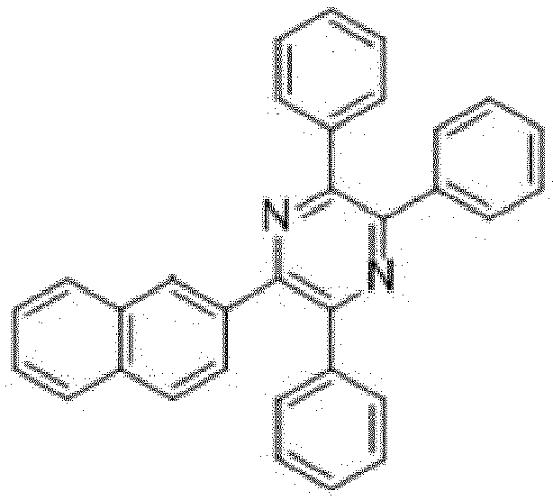
- In case that E is substituted or unsubstituted C4-C70 heteroaryl comprising a triazine group E is bonded to A1 via a direct bond between A1 and the triazine group. For example, in case that E is biphenyltriazine and A1 is naphthylene, the binding situation may be as follows:

- In case that E is C10-C70 aryl comprising at least two condensed benzene rings E is bonded to A1 via a direct bond between A1 and one of the condensed benzene rings. Likewise, in case that E is C4-C70 heteroaryl comprising at least two condensed aromatic rings E is bonded to A1 via a direct bond between A1 and one of the condensed aromatic rings. For example, in case that E is phenyl-quinazoline and A1 is naphthylene, the binding situation may be as follows:

- A1 is selected from the group consisting of a substituted or unsubstituted C10-C70 arylene comprising 2 or 3 condensed rings and a substituted or unsubstituted C2-C70 a heteroarylene comprising 2 or 3 condensed rings; wherein A1 is bonded to E via a direct bond between one of the condensed rings and E; and wherein A1 is bonded to A2 via a direct bond between one of the condensed rings and A2.
- A2 is selected from the group consisting of a substituted or unsubstituted carbocyclic aromatic ring, a substituted or unsubstituted heterocyclic aromatic ring, a substituted or unsubstituted condensed bicyclic aromatic system and a substituted or unsubstituted condensed bicyclic heteroaromatic system; wherein A2 is bonded to A3 via a direct bond between one of the aromatic or heteroaromatic rings and A3.
- In condensed (also called "fused") bicyclic compounds (or bicyclic moieties), two rings share two adjacent atoms.
- A3 is selected from the group consisting of a monocyclic aryl and a monocyclic heteroaryl, wherein A3 is substituted with at least three groups independently selected from the group consisting of substituted or unsubstituted C6-C18 aryl, especially phenyl, and C2-C18 heteroaryl, especially pyridinyl. In this regard, the number of substituents (at least three) does not include the group A2. In other words, A3 has at least three substituents besides A2 (A2 in this context including the moieties A1 and E attached thereto).
- E may be selected from the group consisting of a substituted or unsubstituted C4-C60 heteroaryl comprising a diazine group, a substituted or unsubstituted C3-C60 heteroaryl comprising a triazine group, a C10-C60 aryl comprising at least two condensed benzene rings, and a C4-C60 heteroaryl comprising at least two condensed aromatic rings. E may be selected from the group consisting of a substituted or unsubstituted C4-C50 heteroaryl comprising a diazine group, a substituted or unsubstituted C3-C50 heteroaryl comprising a triazine group, a C10-C50 aryl comprising at least two condensed benzene rings, and a C4-C50 heteroaryl comprising at least two condensed aromatic rings. E may be selected from the group consisting of a substituted or unsubstituted C4-C52 heteroaryl comprising a diazine group, a substituted or unsubstituted C3-C51 heteroaryl comprising a triazine group, a C10-C58 aryl comprising at least two condensed benzene rings, and a C4-C57 heteroaryl comprising at least two condensed aromatic rings. E may be selected from the group consisting of a substituted or unsubstituted C4-C46 heteroaryl comprising a diazine group, a substituted or unsubstituted C3-C45 heteroaryl comprising a triazine group, a C10-C52 aryl comprising at least two condensed benzene rings, and a C4-C51 heteroaryl comprising at least two condensed aromatic rings. E may be selected from the group consisting of a substituted or unsubstituted C4-C40 heteroaryl comprising a diazine group, a substituted or unsubstituted C3-C39 heteroaryl comprising a triazine group, a C10-C46 aryl comprising at least two condensed benzene rings, and a C4-C45 heteroaryl comprising at least two condensed aromatic rings. E may be selected from the group consisting of a substituted or unsubstituted C4-C34 heteroaryl comprising a diazine group, a substituted or unsubstituted C3-C33 heteroaryl comprising a triazine group, a C10-C40 aryl comprising at least two condensed benzene rings, and a C4-C39 heteroaryl comprising at least two condensed aromatic rings. E may be selected from the group consisting of a substituted or unsubstituted C4-C28 heteroaryl comprising a diazine group, a substituted or unsubstituted C3-C27 heteroaryl comprising a triazine group, a C10-C34 aryl comprising at least two condensed benzene rings, and a C4-C33 heteroaryl comprising at least two condensed aromatic rings. E may be selected from the group consisting of a substituted or unsubstituted C4-C22 heteroaryl comprising a diazine group, a substituted or unsubstituted C3-C21 heteroaryl comprising a triazine group, a C10-C28 aryl comprising at least two condensed benzene rings, and a C4-C27 heteroaryl comprising at least two condensed aromatic rings. E may be selected from the group consisting of a substituted or unsubstituted C4-C16 heteroaryl comprising a diazine group, a substituted or unsubstituted C3-C15 heteroaryl comprising a triazine group, a C10-C22 aryl comprising at least two condensed benzene rings, and a C4-C21 heteroaryl comprising at least two condensed aromatic rings.
- E may be selected from the group consisting of pyrimidine, pyrazine, pyridazine, triazine, naphthalene and aza-analogs thereof, especially quinazoline, anthracene and aza-analogs thereof, phenanthrene and aza-analogs thereof, specially benzoquinazoline, fluorene and aza-analogs thereof, benzofluorene and aza-analogs thereof, dibenzofluorene and aza-analogs thereof, naphtofluorene and aza-analogs thereof, benzo-naphtofluorene and aza-analogs thereof, dinaphtofluorene and aza-analogs thereof, benzimidazole and aza analogs thereof, benzoxazole and aza analogs thereof, benzothiazole and aza analogs thereof, pyrido-imidazole and aza analogs thereof, benzofurane and aza-analogs thereof, benzothiophene and aza-analogs thereof, dibenzofurane and aza-analogs thereof, dibenzothiophene and aza-analogs thereof, naphtofurane and aza-analogs thereof, naphtothiophene and aza-analogs thereof, naphtobenzofurane and aza-analogs thereof, naphtobenzothiophene and aza-analogs thereof, dinaphtofurane and aza-analogs thereof, dinaphtothiophene and aza-analogs thereof, aryl consisting of 4, 5, 6 or 7 condensed rings and aza-analogs thereof, and heteroaryl consisting of 3, 4, 5, 6 or 7 condensed rings and comprising 1, 2 or 3 ring atoms independently selected from O and S, and aza-analogs of the heteroaryl consisting of 3, 4, 5, 6 or 7 condensed rings and comprising 1, 2 or 3 ring atoms independently selected from O and S, wherein the groups may be substituted or unsubstituted respectively, especially with one or more phenyl and/or pyridyl groups, wherein the phenyl and/or pyridyl groups may be substituted or unsubstituted.
- The term "aza-analog" as used herein refers to a respective group in which one or more of the carbon atoms of the group are replaced by nitrogen atoms. For example, aza-analogs of naphthalene


- E may be selected from the group consisting of pyrimidine, pyrazine, cinnoline, quioline, phtalazine, quinoxaline, quinazoline, benzoquinazoline, pyrido-imidazole, benzimidazole, pyrido-benzimidazole and 1,3,5-triazine, wherein the groups may be substituted or unsubstituted, respectively.
- E may be selected from the group consisting of pyrimidine, pyrazine, quinazoline, benzoquinazoline, and 1,3,5-triazine, wherein the groups may be substituted or unsubstituted, respectively, especially may be substituted with one or more unsubstituted phenyl.
- E (including the substituents) may be selected from the group consisting of


- A1 may be selected from the group consisting of a substituted or unsubstituted C10-C58 arylene comprising 2 or 3 condensed rings and a substituted or unsubstituted C2-C57 a heteroarylene comprising 2 or 3 condensed rings. A1 may be selected from the group consisting of a substituted or unsubstituted C10-C52 arylene comprising 2 or 3 condensed rings and a substituted or unsubstituted C2-C51 a heteroarylene comprising 2 or 3 condensed rings. A1 may be selected from the group consisting of a substituted or unsubstituted C10-C46 arylene comprising 2 or 3 condensed rings and a substituted or unsubstituted C2-C45 a heteroarylene comprising 2 or 3 condensed rings. A1 may be selected from the group consisting of a substituted or unsubstituted C10-C40 arylene comprising 2 or 3 condensed rings and a substituted or unsubstituted C2-C39 a heteroarylene comprising 2 or 3 condensed rings. A1 may be selected from the group consisting of a substituted or unsubstituted C10-C34 arylene comprising 2 or 3 condensed rings and a substituted or unsubstituted C2-C33 a heteroarylene comprising 2 or 3 condensed rings. A1 may be selected from the group consisting of a substituted or unsubstituted C10-C28 arylene comprising 2 or 3 condensed rings and a substituted or unsubstituted C2-C27 a heteroarylene comprising 2 or 3 condensed rings. A1 may be selected from the group consisting of a substituted or unsubstituted C10-C22 arylene comprising 2 or 3 condensed rings and a substituted or unsubstituted C2-C21 a heteroarylene comprising 2 or 3 condensed rings. A1 may be selected from the group consisting of a substituted or unsubstituted C10-C16 arylene comprising 2 or 3 condensed rings and a substituted or unsubstituted C2-C15 a heteroarylene comprising 2 or 3 condensed rings.
- A1 may be selected from the group consisting of a substituted or unsubstituted C10-C58 arylene comprising 2 or 3 condensed rings. A1 may be selected from the group consisting of a substituted or unsubstituted C10-C52 arylene comprising 2 or 3 condensed rings. A1 may be selected from the group consisting of a substituted or unsubstituted C10-C46 arylene comprising 2 or 3 condensed rings. A1 may be selected from the group consisting of a substituted or unsubstituted C10-C40 arylene comprising 2 or 3 condensed rings. A1 may be selected from the group consisting of a substituted or unsubstituted C10-C34 arylene comprising 2 or 3 condensed rings. A1 may be selected from the group consisting of a substituted or unsubstituted C10-C28 arylene comprising 2 or 3 condensed rings. A1 may be selected from the group consisting of a substituted or unsubstituted C10-C22 arylene comprising 2 or 3 condensed rings. A1 may be selected from the group consisting of a substituted or unsubstituted C10-C16 arylene comprising 2 or 3 condensed rings.
- A1 may selected from the group consisting of naphtalene-diyl and aza-analogs thereof, anthracene-diyl and aza-analogs thereof, phenanthrene-diyl and aza-analogs thereof, fluorene-diyl and aza-analogs thereof, benzothiophene-diyl and aza-analogs thereof, benzofurane-diyl and aza-analogs thereof, naphtofurane-diyl and aza-analogs thereof, naphtothiophene-diyl and aza-analogs thereof, dibenzofurane-diyl aza-analogs thereof, and dibenzothiophene-diyl and aza-analogs thereof.
- A1 may selected from the group consisting of naphtalene-diyl and aza-analogs thereof, and phenanthrene-diyl and aza-analogs thereof.
- A1 may be selected from the group consisting of naphtalene-1,2-diyl, naphtalene-1,3-diyl, naphtalene-1,4-diyl, naphtalene-1,5-diyl, naphtalene-1,6-diyl, naphtalene-1,7-diyl, naphtalene-1,8-diyl, naphtalene-2,3-diyl, and naphtalene-2,6-diyl, naphtalene-2,7-diyl, and phenanthrene-9,10-diyl.
- A2 may be selected from the group consisting of phenylene, thiophenylene, furanylene, pyrazolylene, imidazolylene, triazolylene, pyridinylene, pyrimidinylene, pyridazinylene, pyrazinelyen and triazinylene.
- A2 may be selected from the group consisting of o-phenylene, m-phenylene, p-phenylene, and pyridine-3,5-ylene.
- A3 (not including the at least three groups by which Ar3 is substituted) may be selected from the group consisting of phenyl, thiophenyl, furanyl, pyridinyl, pyrimidinyl, pyridazinyl, and pyrazinyl.
- A3 (not including the at least three groups by which Ar3 is substituted) may be selected from the group consisting of phenyl, pyridinyl, pyrimidinyl and pyrazinyl.
- A3 (not including the at least three groups by which Ar3 is substituted) may be selected from the group consisting of phenyl, pyrimidinyl and pyrazinyl.
- The at least three groups by which A3 is substituted may be independently selected from the group consisting of unsubstituted phenyl, phenyl substituted with one or more hydrocarbyl groups, wherein the total number of carbon atoms in the phenyl substituted with one or more hydrocarbyl groups is from 7 to 18, pyridyl, pyridyl substituted with one or more hydrocarbyl groups, wherein the total number of carbon atoms in the phenyl substituted with one or more hydrocarbyl groups is from 7 to 18, and CN-substituted phenyl.
- The at least three groups by which A3 is substituted may be independently selected from the group consisting of unsubstituted phenyl, CN-substituted phenyl, especially meta-CN-substituted phenyl, pyridyl, and picoline (methylpyridyl, for example 2-methylpyridyl, 3-methylpyridyl or 4-methylpyridyl).
- The at least three groups by which A3 is substituted may be independently selected from the group consisting of

- A3 (including the at least three groups by which Ar3 is substituted) may be selected from the group consisting of


- The compound of formula (I) may be selected from the following compounds E1 to E20


- In the following specific embodiments of the compound of formula (I) are described wherein these embodiments may be combined with one or more of the above features.
- In one embodiment, the invention relates to a compound having the formula (I)
E-A1-A2-A3 (I),
- wherein in formula (I)
- E is selected from the group consisting of a substituted or unsubstituted C4-C16 heteroaryl comprising a diazine group, a substituted or unsubstituted C3-C15 heteroaryl comprising a triazine group, a C10-C22 aryl comprising at least two condensed benzene rings, and a C4-C21 heteroaryl comprising at least two condensed aromatic rings;
- A1 is selected from the group consisting of a substituted or unsubstituted C10-C16 arylene comprising 2 or 3 condensed rings and a substituted or unsubstituted C2-C15 a heteroarylene comprising 2 or 3 condensed rings;
- A2 is selected from the group consisting of phenylene, thiophenylene, furanylene, pyrazolylene, imidazolylene, triazolylene, pyridinylene, pyrimidinylene, pyridazinylene, pyrazinelyen and triazinylene; and
- A3 is selected from the group consisting of phenyl, thiophenyl, furanyl, pyridinyl, pyrimidinyl, pyridazinyl, and pyrazinyl, wherein Ar3 is substituted with at least three groups, wherein the at least three groups by which A3 is substituted are independently selected from the group consisting of unsubstituted phenyl, phenyl substituted with one or more hydrocarbyl groups, wherein the total number of carbon atoms in the phenyl substituted with one or more hydrocarbyl groups is from 7 to 18, pyridyl, pyridyl substituted with one or more hydrocarbyl groups, wherein the total number of carbon atoms in the phenyl substituted with one or more hydrocarbyl groups is from 7 to 18, and CN-substituted phenyl;
- wherein the groups E, A1, A2 and A3 are connected with each other via direct bonds (single bonds) as set forth above.
- In one embodiment, the invention relates to a compound having the formula (I)
E-A1-A2-A3 (I),
- wherein in formula (I)
- E is selected from the group consisting of pyrimidine, pyrazine, cinnoline, quinoline, phtalazine, quinoxaline, quinazoline, benzoquinazoline, pyrido-imidazole, benzimidazole, pyrido-benzimidazole and 1,3,5-triazine, wherein the groups may be substituted or unsubstituted, respectively;
- A1 is selected from the group consisting of naphtalene-diyl and aza-analogs thereof, anthracene-diyl and aza-analogs thereof, phenanthrene-diyl and aza-analogs thereof, fluorene-diyl and aza-analogs thereof, benzothiophene-diyl and aza-analogs thereof, benzofurane-diyl and aza-analogs thereof, naphtofurane-diyl and aza-analogs thereof, naphtothiophene-diyl and aza-analogs thereof, dibenzofurane-diyl aza-analogs thereof, and dibenzothiophene-diyl and aza-analogs thereof;
- A2 is selected from the group consisting of phenylene, thiophenylene, furanylene, pyrazolylene, imidazolylene, triazolylene, pyridinylene, pyrimidinylene, pyridazinylene, pyrazinelyen and triazinylene; and
- A3 is selected from the group consisting of phenyl, pyridinyl, pyrimidinyl and pyrazinyl; wherein Ar3 is substituted with at least three groups, wherein the at least three groups by which A3 is substituted are independently selected from the group consisting of unsubstituted phenyl, CN-substituted phenyl, especially meta-CN-substituted phenyl, pyridyl, and picoline (2-methylpyridyl);
- wherein the groups E, A1, A2 and A3 are connected with each other via direct bonds (single bonds) as set forth above.
- In one embodiment, the invention relates to a compound having the formula (I)
E-A1-A2-A3 (I),
- wherein in formula (I)
- E (including the substituents) is selected from the group consisting of


- A1 is selected from the group consisting of naphtalene-1,2-diyl, naphtalene-1,3-diyl, naphtalene-1,4-diyl, naphtalene-1,5-diyl, naphtalene-1,6-diyl, naphtalene-1,7-diyl, naphtalene-1,8-diyl, naphtalene-2,3-diyl, and naphtalene-2,6-diyl, naphtalene-2,7-diyl, and phenanthrene-9,10-diyl;
- A2 is selected from the group consisting of o-phenylene, m-phenylene, p-phenylene, and pyridine-3,5-ylene; and
- A3 is substituted may be independently selected from the group consisting of

- E (including the substituents) is selected from the group consisting of
- wherein the asterisk symbol "∗" represents the binding position of the group to A1;
- wherein the groups E, A1, A2 and A3 are connected with each other via direct bonds (single bonds) as set forth above.
- The present invention is further related to a semiconducting material comprising the compound of formula (I) according to the present invention as defined herein. Embodiments with respect to the compound per se are also embodiments for the semiconducting material comprising said compound.
- The semiconducting material may be an electron transport material, that is, a material allowing, for example, in an OLED, transport of electrons from a cathode to a light emitting layer through the electron transport material.
- The semiconducting material may comprise the compound of formula (I) (or two or more of respective compounds) and a further material not having the formula (I).
- The semiconducting material may be an electron transport material and the compound of formula (I) may be an electron transport matrix. In this regard, it may be provided that the compound of formula (I) of formula (I) is the predominant material in the semiconducting material, especially may be doped with at least one electrical n-dopant.
- In this regard, electrical n-dopants are in particular, but not limited thereto, an elemental metal, alternatively an electropositive metal selected from alkali metals, alkaline earth metals, rare earth metals and transition metals, transition metals; a metal salt, alternatively an alkali metal salt, alkaline earth metal salt and/or rare earth metal salt, or a metal complex, alternatively an alkali metal complex, alkaline earth metal complex, transition metal complex and/or rare earth metal complex. Examples of n-doping metal salts can be LiF, LiCl, LiBr, Lil, metal borates, metal quinolinolates or mixtures thereof. Further examples of electrical n-dopants are strong chemical reducing agents. This class of "redox" n-dopants may be generically characterized by energy level of the highest occupied molecular orbital (HOMO) comparable with lowest unoccupied molecular orbital energy level of corresponding electron transport matrices, which can, in usual OLED transport materials, have a value about -3.0 eV or less negative.
- Electrical n-dopants may be organic compounds as disclosed in
EP1837926A1 ,WO07107306A1 WO07107356A1 - The invention further relates to an electronic device comprising at least one layer comprising the compound of formula (I) according to the present invention as defined herein. Embodiments with respect to the compound per se are also embodiments for the semiconducting material comprising said compound.
- The electronic device according to the present invention may be an organic electronic device. The organic electronic device according to the invention may be an organic light-emitting device.
- The organic electronic device may comprise an electron transport layer, wherein the compound of formula (I) is comprised in the electron transport layer.
- The organic electronic device may comprise a cathode, a light emitting layer and an electron transport layer, wherein the electron transport layer is arranged between the cathode and the light emitting layers, and the compound of formula (I) is comprised in the electron transport layer.
- The organic electronic device may comprise a cathode, a light emitting layer and an electron transport layer, wherein the electron transport layer is arranged between the cathode and the light emitting layer, and the compound of formula (I) is comprised in the electron transport layer.
- The organic electronic device may comprise a cathode, a light emitting layer and an electron transport layer, wherein the electron transport layer is arranged between the cathode and the light emitting layer, the electron transport layer is in direct contact with the light emitting layer and the compound of formula (I) is comprised in the electron transport layer.
- According to one aspect of the present invention, there is provided an organic light-emitting diode (OLED) comprising: a substrate; an anode electrode formed on the substrate; a hole injection layer, a hole transport layer, an emission layer, an electron transport layer, the electron injection layer and a cathode electrode, wherein the compound of formula (I) is comprised in the electron transport layer or in the electron injection layer.
- According to one aspect of the present invention, there is provided an organic light-emitting diode (OLED) comprising: a substrate; an anode electrode formed on the substrate; a hole injection layer, a hole transport layer, an electron blocking layer, an emission layer, an electron transport layer, the electron injection layer and a cathode electrode, wherein the compound of formula (I) is comprised in the electron transport layer or in the electron injection layer.
- According to another aspect of the present invention, there is provided an OLED comprising: a substrate; an anode electrode formed on the substrate; a hole injection layer, a hole transport layer, an electron blocking layer, an emission layer, a hole blocking layer, an electron transport layer, the electron injection layer and a cathode electrode, wherein the compound of formula (I) is comprised in hole blocking layer, the electron transport layer or in the electron injection layer, especially in the hole blocking layer.
- According to another aspect of the present invention, there is provided an OLED comprising: a substrate; an anode electrode formed on the substrate; a hole injection layer, a hole transport layer, an electron blocking layer, an emission layer, a hole blocking layer, an electron transport layer, an electron injection layer, and a cathode electrode, wherein the compound of formula (I) is comprised in hole blocking layer, the electron transport layer or in the electron injection layer, especially in the hole blocking layer.
- The present invention further relates to a display comprising a light emitting diode, wherein the light emitting diode comprises the compound of formula (I) according to the present invention as defined herein. Embodiments with respect to the compound per se are also embodiments for the semiconducting material comprising said compound.
- In accordance with the invention, the (organic) electronic device may comprise, besides the layers already mentioned above, further layers. Exemplary embodiments of respective layers are described in the following:
- The substrate may be any substrate that is commonly used in manufacturing of, electronic devices, such as organic light-emitting diodes. If light is to be emitted through the substrate, the substrate shall be a transparent or semitransparent material, for example a glass substrate or a transparent plastic substrate. If light is to be emitted through the top surface, the substrate may be both a transparent as well as a non-transparent material, for example a glass substrate, a plastic substrate, a metal substrate or a silicon substrate.
- Either a first electrode or a second electrode comprised in the inventive organic electronic device may be an anode electrode. The anode electrode may be formed by depositing or sputtering a material that is used to form the anode electrode. The material used to form the anode electrode may be a high work-function material, so as to facilitate hole injection. The anode material may also be selected from a low work function material (i.e. aluminum). The anode electrode may be a transparent or reflective electrode. Transparent conductive oxides, such as indium tin oxide (ITO), indium zinc oxide (IZO), tin-dioxide (SnO2), aluminum zinc oxide (AlZO) and zinc oxide (ZnO), may be used to form the anode electrode. The anode electrode may also be formed using metals, typically silver (Ag), gold (Au), or metal alloys. The transparent or semitransparent anode may facilitate light emission through the anode.
- A hole injection layer (HIL) may be formed on the anode electrode by vacuum deposition, spin coating, printing, casting, slot-die coating, Langmuir-Blodgett (LB) deposition, or the like. When the HIL is formed using vacuum deposition, the deposition conditions may vary according to the compound that is used to form the HIL, and the desired structure and thermal properties of the HIL. In general, however, conditions for vacuum deposition may include a deposition temperature of 100° C to 500° C, a pressure of 10-8 to 10-3 Torr (1 Torr equals 133.322 Pa), and a deposition rate of 0.1 to 10 nm/sec.
- When the HIL is formed using spin coating or printing, coating conditions may vary according to the compound that is used to form the HIL, and the desired structure and thermal properties of the HIL. For example, the coating conditions may include a coating speed of about 2000 rpm to about 5000 rpm, and a thermal treatment temperature of about 80° C to about 200° C. Thermal treatment removes a solvent after the coating is performed.
- The HIL may be formed of any compound that is commonly used to form a HIL. Examples of compounds that may be used to form the HIL include a phthalocyanine compound, such as copper phthalocyanine (CuPc), 4,4',4"-tris (3-methylphenylphenylamino) triphenylamine (m-MTDATA), TDATA, 2T-NATA, polyaniline/dodecylbenzenesulfonic acid (Pani/DBSA), poly(3,4-ethylenedioxythiophene)/poly(4-styrenesulfonate) (PEDOT/PSS), polyaniline/camphor sulfonic acid (Pani/CSA), and polyaniline)/poly(4-styrenesulfonate (PANI/PSS).
- The HIL may comprise or consist of p-type dopant and the p-type dopant may be selected from tetrafluoro-tetracyanoquinonedimethane (F4TCNQ), 2,2'-(perfluoronaphthalen-2,6-diylidene)-dimalononitrile, 4,4',4"-((1E,1'E,1"E)-cyclopropane-1,2,3-triylidenetris(cyanomethanylylidene))tris(2,3,5,6-tetrafluorobenzonitrile) or 2,2',2"-(cyclopropane-1,2,3-triylidene)tris(2-(p-cyanotetrafluorophenyl)acetonitrile) but not limited hereto. The HIL may be selected from a hole-transporting matrix compound doped with a p-type dopant. Typical examples of known doped hole transport materials are: copper phthalocyanine (CuPc), which HOMO level is approximately -5.2 eV, doped with tetrafluoro-tetracyanoquinonedimethane (F4TCNQ), which LUMO level is about -5.2 eV; zinc phthalocyanine (ZnPc) (HOMO = -5.2 eV) doped with F4TCNQ; α-NPD (N,N'-Bis(naphthalen-1-yl)-N,N'-bis(phenyl)-benzidine) doped with F4TCNQ. α-NPD doped with 2,2'-(perfluoronaphthalen-2,6-diylidene) dimalononitrile. The p-type dopant concentrations can be selected from 1 to 20 wt.-%, more preferably from 3 wt.-% to 10 wt.-%.
- The thickness of the HIL may be in the range from about 1 nm to about 100 nm, and for example, from about 1 nm to about 25 nm. When the thickness of the HIL is within this range, the HIL may have excellent hole injecting characteristics, without a substantial penalty in driving voltage.
- A hole transport layer (HTL) may be formed on the HIL by vacuum deposition, spin coating, slot-die coating, printing, casting, Langmuir-Blodgett (LB) deposition, or the like. When the HTL is formed by vacuum deposition or spin coating, the conditions for deposition and coating may be similar to those for the formation of the HIL. However, the conditions for the vacuum or solution deposition may vary, according to the compound that is used to form the HTL.
- The HTL may be formed of any compound that is commonly used to form a HTL. Compounds that can be suitably used are disclosed for example in Yasuhiko Shirota and Hiroshi Kageyama, Chem. Rev. 2007, 107, 953-1010 and incorporated by reference. Examples of the compound that may be used to form the HTL are: carbazole derivatives, such as N-phenylcarbazole or polyvinylcarbazole; benzidine derivatives, such as N,N'-bis(3-methylphenyl)-N,N'-diphenyl-[1,1-biphenyl]-4,4'-diamine (TPD), or N,N'-di(naphthalen-1-yl)-N,N'-diphenyl benzidine (alpha-NPD); and triphenylamine-based compound, such as 4,4',4"-tris(N-carbazolyl)triphenylamine (TCTA). Among these compounds, TCTA can transport holes and inhibit excitons from being diffused into the EML.
- The thickness of the HTL may be in the range of about 5 nm to about 250 nm, preferably, about 10 nm to about 200 nm, further about 20 nm to about 190 nm, further about 40 nm to about 180 nm, further about 60 nm to about 170 nm, further about 80 nm to about 160 nm, further about 100 nm to about 160 nm, further about 120 nm to about 140 nm. A preferred thickness of the HTL may be 170 nm to 200 nm.
- When the thickness of the HTL is within this range, the HTL may have excellent hole transporting characteristics, without a substantial penalty in driving voltage.
- The function of an electron blocking layer (EBL) is to prevent electrons from being transferred from an emission layer to the hole transport layer and thereby confine electrons to the emission layer. Thereby, efficiency, operating voltage and/or lifetime are improved. Typically, the electron blocking layer comprises a triarylamine compound. The triarylamine compound may have a LUMO level closer to vacuum level than the LUMO level of the hole transport layer. The electron blocking layer may have a HOMO level that is further away from vacuum level compared to the HOMO level of the hole transport layer. The thickness of the electron blocking layer may be selected between 2 and 20 nm.
- If the electron blocking layer has a high triplet level, it may also be described as triplet control layer.
- The function of the triplet control layer is to reduce quenching of triplets if a phosphorescent green or blue emission layer is used. Thereby, higher efficiency of light emission from a phosphorescent emission layer can be achieved. The triplet control layer is selected from triarylamine compounds with a triplet level above the triplet level of the phosphorescent emitter in the adjacent emission layer. Suitable compounds for the triplet control layer, in particular the triarylamine compounds, are described in
EP 2 722 908 A1 . - The EML may be formed on the HTL by vacuum deposition, spin coating, slot-die coating, printing, casting, LB deposition, or the like. When the EML is formed using vacuum deposition or spin coating, the conditions for deposition and coating may be similar to those for the formation of the HIL. However, the conditions for deposition and coating may vary, according to the compound that is used to form the EML.
- It may be provided that the emission layer does not comprise the compound of formula (I).
- The emission layer (EML) may be formed of a combination of a host and an emitter dopant. Example of the host are Alq3, 4,4'-N,N'-dicarbazole-biphenyl (CBP), poly(n-vinylcarbazole) (PVK), 9,10-di(naphthalene-2-yl)anthracene (ADN), 4,4',4"-tris(carbazol-9-yl)-triphenylamine(TCTA), 1,3,5-tris(N-phenylbenzimidazole-2-yl)benzene (TPBI), 3-tert-butyl-9,10-di-2-naphthylanthracenee (TBADN), distyrylarylene (DSA) and bis(2-(2-hydroxyphenyl)benzo-thiazolate)zinc (Zn(BTZ)2).
- The emitter dopant may be a phosphorescent or fluorescent emitter. Phosphorescent emitters and emitters which emit light via a thermally activated delayed fluorescence (TADF) mechanism may be preferred due to their higher efficiency. The emitter may be a small molecule or a polymer.
- Examples of red emitter dopants are PtOEP, Ir(piq)3, and Btp2lr(acac), but are not limited thereto. These compounds are phosphorescent emitters, however, fluorescent red emitter dopants could also be used.
- Examples of phosphorescent green emitter dopants are Ir(ppy)3 (ppy = phenylpyridine), Ir(ppy)2(acac), Ir(mpyp)3.
- Examples of phosphorescent blue emitter dopants are F2Irpic, (F2ppy)2Ir(tmd) and Ir(dfppz)3 and ter-fluorene. 4.4'-bis(4-diphenyl amiostyryl)biphenyl (DPAVBi), 2,5,8,11-tetra-tert-butyl perylene (TBPe) are examples of fluorescent blue emitter dopants.
- The amount of the emitter dopant may be in the range from about 0.01 to about 50 parts by weight, based on 100 parts by weight of the host. Alternatively, the emission layer may consist of a light-emitting polymer. The EML may have a thickness of about 10 nm to about 100 nm, for example, from about 20 nm to about 60 nm. When the thickness of the EML is within this range, the EML may have excellent light emission, without a substantial penalty in driving voltage.
- A hole blocking layer (HBL) may be formed on the EML, by using vacuum deposition, spin coating, slot-die coating, printing, casting, LB deposition, or the like, in order to prevent the diffusion of holes into the ETL. When the EML comprises a phosphorescent dopant, the HBL may have also a triplet exciton blocking function. The HBL may also be named auxiliary ETL or a-ETL.
- When the HBL is formed using vacuum deposition or spin coating, the conditions for deposition and coating may be similar to those for the formation of the HIL. However, the conditions for deposition and coating may vary, according to the compound that is used to form the HBL. Any compound that is commonly used to form a HBL may be used. Examples of compounds for forming the HBL include oxadiazole derivatives, triazole derivatives, and phenanthroline derivatives.
- The HBL may have a thickness in the range from about 5 nm to about 100 nm, for example, from about 10 nm to about 30 nm. When the thickness of the HBL is within this range, the HBL may have excellent hole-blocking properties, without a substantial penalty in driving voltage.
- The compound of formula (I) may comprised in the HBL.
- The OLED according to the present invention may comprise an electron transport layer (ETL).
- According to various embodiments the OLED may comprise an electron transport layer or an electron transport layer stack comprising at least a first electron transport layer and at least a second electron transport layer.
- By suitably adjusting energy levels of particular layers of the ETL, the injection and transport of the electrons may be controlled, and the holes may be efficiently blocked. Thus, the OLED may have long lifetime.
- The electron transport layer may comprise suitable ETM materials known in the art. In accordance with the invention, the electron transport layer may comprise, besides the ETM material, at least one additive as defined herein.
- Further, the electron transport layer may (or may not) comprise one or more n-type dopants. The additive may be an n-type dopant. The additive can be alkali metal, alkali metal compound, alkaline earth metal, alkaline earth metal compound, transition metal, transition metal compound or a rare earth metal. In another embodiment, the metal can be one selected from a group consisting of Li, Na, K, Rb, Cs, Mg, Ca, Sr, Ba, La, Ce, Sm, Eu, Tb, Dy, and Yb. In another embodiment, the n-type dopant can be one selected from a group consisting of Cs, K, Rb, Mg, Na, Ca, Sr, Eu and Yb. In an embodiment the alkali metal compound may be 8-Hydroxyquinolinolato-lithium (LiQ), Lithium tetra(1H-pyrazol-1-yl)borate or Lithium 2-(diphenylphosphoryl)phenolate. Suitable compounds for the ETM are not particularly limited. In one embodiment, the electron transport matrix compounds consist of covalently bound atoms. Preferably, the electron transport matrix compound comprises a conjugated system of at least 6, more preferably of at least 10 delocalized electrons. In one embodiment, the conjugated system of delocalized electrons may be comprised in aromatic or heteroaromatic structural moieties, as disclosed e.g. in documents
EP 1 970 371 A1 orWO 2013/079217 A1 . - The compound of formula (I) may comprised in the electron transport layer.
- An optional EIL, which may facilitates injection of electrons from the cathode, may be formed on the ETL, preferably directly on the electron transport layer. Examples of materials for forming the EIL include lithium 8-hydroxyquinolinolate (LiQ), LiF, NaCl, CsF, Li2O, BaO, Ca, Ba, Yb, Mg which are known in the art. Deposition and coating conditions for forming the EIL are similar to those for formation of the HIL, although the deposition and coating conditions may vary, according to the material that is used to form the EIL.
- The thickness of the EIL may be in the range from about 0.1 nm to about 10 nm, for example, in the range from about 0.5 nm to about 9 nm. When the thickness of the EIL is within this range, the EIL may have satisfactory electron-injecting properties, without a substantial penalty in driving voltage.
- The EIL may consist of a number of individual EIL sublayers. In case the EIL consists of a number of individual EIL sublayers, the number of sublayers is preferably 2. The individual EIL sublayers may comprise different materials for forming the EIL.
- The thickness of the EIL may be in the range from about 0.1 nm to about 10 nm, for example, in the range from about 0.5 nm to about 9 nm. When the thickness of the EIL is within this range, the EIL may have satisfactory electron-injecting properties, without a substantial penalty in driving voltage.
- The cathode electrode is formed on the EIL if present, preferably directly on the EIL, preferably in direct contact with the EIL. In the sense of this invention the cathode and the EIL can be regarded as one functional part enabling the injection of electrons into the electron transport layer. The cathode electrode may be formed of a metal, an alloy, an electrically conductive compound, or a mixture thereof. The cathode electrode may have a low work function. For example, the cathode electrode may be formed of lithium (Li), magnesium (Mg), aluminum (Al), aluminum (Al)-lithium (Li), calcium (Ca), barium (Ba), ytterbium (Yb), magnesium (Mg)-indium (In), magnesium (Mg)-silver (Ag), or the like. Alternatively, the cathode electrode may be formed of a transparent conductive oxide, such as ITO or IZO.
- The thickness of the cathode electrode may be in the range from about 5 nm to about 1000 nm, for example, in the range from about 10 nm to about 100 nm. When the thickness of the cathode electrode is in the range from about 5 nm to about 50 nm, the cathode electrode may be transparent or semitransparent even if formed from a metal or metal alloy. The transparent or semitransparent cathode may facilitate light emission through the cathode.
- It is to be understood that the cathode electrode is not part of the electron injection layer.
- A charge generation layer (CGL) may be comprised in the inventive OLED. This layer may comprise a p-type CGL and an n-type CGL. An interlayer may be arranged between the p-type layer and the n-type layer.
- Typically, the charge generation layer GCL is a pn-junction joining an n-type charge generation layer (electron generating layer, n-type CGL) and a-type charge generation layer (hole generating layer, p-type CGL). The n-side of the pn-junction generates electrons and injects them into the layer which is adjacent in the direction to the anode. Analogously, the p-side of the pn-junction generates holes and injects them into the layer which is adjacent in the direction to the cathode.
- Charge generation layers are used in tandem OLEDs comprising, between the cathode and anode, two or more emission layers. In a tandem OLED comprising two emission layers, the n-type charge generation layer provides electrons for the first light emission layer arranged near the anode, while the hole generating layer provides holes to the second light emission layer arranged between the first emission layer and the cathode.
- Suitable matrix materials for the hole generating layer may be materials conventionally used as hole injection and/or hole transport matrix materials. Also, p-type dopant used for the hole generating layer can employ conventional materials. For example, the p-type dopant can be one selected from a group consisting of tetrafluore-7,7,8,8-tetracyanoquinodimethane (F4-TCNQ), derivatives of tetracyanoquinodimethane, radialene derivatives, iodine, FeCl3, FeF3, and SbCl5. Also, the host can be one selected from a group consisting of N,N'-di(naphthalen-i-yl)-N,N-diphenyl-benzidine (NPB), N,N'-diphenyl-N,N'-bis(3-methylphenyl)-1,1-biphenyl-4,4'-diamine (TPD) and N,N',N'-tetranaphthyl-benzidine (TNB). The p-type charge generation layer may consist of CNHAT.
- The n-type charge generation layer may be layer of a neat n-type dopant, for example of an electropositive metal, or can consist of an organic matrix material doped with the n-type dopant. In one embodiment, the n-type dopant can be alkali metal, alkali metal compound, alkaline earth metal, alkaline earth metal compound, a transition metal, a transition metal compound or a rare earth metal. In another embodiment, the metal can be one selected from a group consisting of Li, Na, K, Rb, Cs, Mg, Ca, Sr, Ba, La, Ce, Sm, Eu, Tb, Dy, and Yb. More specifically, the n-type dopant can be one selected from a group consisting of Cs, K, Rb, Mg, Na, Ca, Sr, Eu and Yb. Suitable matrix materials for the n-type charge generation layer layer may be the materials conventionally used as matrix materials for electron injection or electron transport layers. The matrix material can be for example one selected from a group consisting of N-containing heterocyclic compounds like triazine compounds or phenathroline compounds such as compound E or bipyridyl or terpyridyl compounds, hydroxyquinoline derivatives like tris(8-hydroxyquinoline)aluminum, benzazole derivatives, and silole derivatives.
- The organic electronic device according to the invention may be an organic light-emitting device.
- According to one aspect of the present invention, there is provided an organic light-emitting diode (OLED) comprising: a substrate; an anode electrode formed on the substrate; a hole injection layer, a hole transport layer, an emission layer, an electron transport layer, the electron injection layer and a cathode electrode.
- According to one aspect of the present invention, there is provided an organic light-emitting diode (OLED) comprising: a substrate; an anode electrode formed on the substrate; a hole injection layer, a hole transport layer, an electron blocking layer, an emission layer, an electron transport layer, the electron injection layer and a cathode electrode.
- According to another aspect of the present invention, there is provided an OLED comprising: a substrate; an anode electrode formed on the substrate; a hole injection layer, a hole transport layer, an electron blocking layer, an emission layer, a hole blocking layer, an electron transport layer, the electron injection layer and a cathode electrode.
- According to another aspect of the present invention, there is provided an OLED comprising: a substrate; an anode electrode formed on the substrate; a hole injection layer, a hole transport layer, an electron blocking layer, an emission layer, a hole blocking layer, an electron transport layer, an electron injection layer, and a cathode electrode.
- According to various embodiments of the present invention, there may be provided OLED layers arranged between the above mentioned layers, on the substrate or on the top electrode.
- According to one aspect, the OLED can comprise a layer structure of a substrate that is adjacent arranged to an anode electrode, the anode electrode is adjacent arranged to a first hole injection layer, the first hole injection layer is adjacent arranged to a first hole transport layer, the first hole transport layer is adjacent arranged to a first electron blocking layer, the first electron blocking layer is adjacent arranged to a first emission layer, the first emission layer is adjacent arranged to an electron transport layer, which may optionally be formed by two sub-layer, which are a first electron transport layer and a second electron transport layer, the first electron transport layer is adjacent arranged to a second electron transport layer, the second electron transport layer is adjacent arranged to an electron injection layer, the electron injection layer is adjacent arranged to the cathode electrode.
- According to another aspect of the present invention, there is provided a method of manufacturing an organic electronic device, the method using:
- at least one deposition source, preferably two deposition sources and more preferred at least three deposition sources.
- The methods for deposition that can be suitable comprise:
- deposition via vacuum thermal evaporation;
- deposition via solution processing, preferably the processing is selected from spin-coating, printing, casting; and/or
- slot-die coating.
- According to various embodiments of the present invention, the method may further include forming on the anode electrode, an emission layer and at least one layer selected from the group consisting of forming a hole injection layer, forming a hole transport layer, or forming an electron hole blocking layer, between the anode electrode and the first electron transport layer.
- According to various embodiments of the present invention, the method may further include the steps for forming an organic light-emitting diode (OLED), wherein
- on a substrate a first anode electrode is formed,
- on the first anode electrode an emission layer is formed,
- on the emission layer an electron transport layer is formed, optionally a hole blocking layer is formed on the emission layer and on the electron transport layer an electro injection layer is formed,
- and finally a cathode electrode is formed,
- optional a hole injection layer, a hole transport layer, and a hole blocking layer, formed in that order between the first anode electrode and the emission layer,
- an electron injection layer is formed between the electron transport layer and the cathode electrode.
- The method comprises forming an electron injection layer on the organic semiconducting layer. According to various embodiments, the OLED may have the following layer structure, wherein the layers having the following order:
anode, hole injection layer, first hole transport layer, second hole transport layer, emission layer, optional hole blocking layer, an electron transport layer, the electron injection layer, and cathode. - According to another aspect of the invention, it is provided an electronic device comprising at least one organic light emitting device according to any embodiment described throughout this application, preferably, the electronic device comprises the organic light emitting diode in one of embodiments described throughout this application. More preferably, the electronic device is a display device.
- In one embodiment, the organic electronic device according to the invention may further comprise a layer comprising a radialene compound and/or a quinodimethane compound.
- In one embodiment, the radialene compound and/or the quinodimethane compound may be substituted with one or more halogen atoms and/or with one or more electron withdrawing groups. Electron withdrawing groups can be selected from nitrile groups, halogenated alkyl groups, alternatively from perhalogenated alkyl groups, alternatively from perfluorinated alkyl groups. Other examples of electron withdrawing groups may be acyl, sulfonyl groups or phosphoryl groups.
- Alternatively, acyl groups, sulfonyl groups and/or phosphoryl groups may comprise halogenated and/or perhalogenated hydrocarbyl. In one embodiment, the perhalogenated hydrocarbyl may be a perfluorinated hydrocarbyl. Examples of a perfluorinated hydrocarbyl can be perfluormethyl, perfluorethyl, perfluorpropyl, perfluorisopropyl, perfluorobutyl, perfluorophenyl, perfluorotolyl; examples of sulfonyl groups comprising a halogenated hydrocarbyl may be trifluoromethylsulfonyl, pentafluoroethylsulfonyl, pentafluorophenylsulfonyl, heptafluoropropylsufonyl, nonafluorobutylsulfonyl, and like.
- In one embodiment, the radialene and/or the quinodimethane compound may be comprised in a hole injection, hole transporting and/or a hole generation layer.
- In one embodiment, the radialene compound may have Formula (XX) and/or the quinodimethane compound may have Formula (XXIa) or (XXIb):

- In the present specification, when a definition is not otherwise provided, an "alkyl group" may refer to an aliphatic hydrocarbon group. The alkyl group may refer to "a saturated alkyl group" without any double bond or triple bond. The term "alkyl" as used herein shall encompass linear as well as branched and cyclic alkyl. For example, C3-alkyl may be selected from n-propyl and iso-propyl. Likewise, C4-alkyl encompasses n-butyl, sec-butyl and t-butyl. Likewise, C6-alkyl encompasses n-hexyl and cyclo-hexyl.
- As used herein if not explicitly mentioned else, the asterisk symbol "∗" represents a binding position at which the moiety labelled accordingly is bond to another moiety.
- The subscribed number n in Cn relates to the total number of carbon atoms in the respective alkyl, arylene, heteroarylene or aryl group.
- The term "aryl" or "arylene" as used herein shall encompass phenyl (C6-aryl), fused aromatics, such as naphthalene, anthracene, phenanthrene, tetracene etc.. Further encompassed are biphenyl and oligo- or polyphenyls, such as terphenyl, phenyl-substituted biphenyl, phenyl-substituted terphenyl (such as tetraphenyl benzole groups) etc.. "Arylene" respectively "heteroarylene", refers to groups to which two further moieties are attached. In the present specification, the term "aryl group" or "arylene group" may refer to a group comprising at least one hydrocarbon aromatic moiety, and all the elements of the hydrocarbon aromatic moiety may have p-orbitals which form conjugation, for example a phenyl group, a napthyl group, an anthracenyl group, a phenanthrenyl group, a pyrinyl group, a fluorenyl group and the like. Further encompoassed are spiro compounds in which two aromatic moieties are connected with each other via a spiro-atom, such as 9,9'-spirobi[9H-fluorene]yl. The aryl or arylene group may include a monocyclic or fused ring polycyclic (i.e., links sharing adjacent pairs of carbon atoms) functional group.
- The term "heteroaryl" as used herein refers to aryl groups in which at least one carbon atom is substituted with a heteroatom. The term "heteroaryl" may refer to aromatic heterocycles with at least one heteroatom, and all the elements of the hydrocarbon heteroaromatic moiety may have p-orbitals which form conjugation. The heteroatom may be selected from N, O, S, B, Si, P, Se, preferably from N, O and S. A heteroarylene ring may comprise at least 1 to 3 heteroatoms. Preferably, a heteroarylene ring may comprise at least 1 to 3 heteroatoms individually selected from N, S and/or O. Just as in case of "aryl"/"arylene", the term "heteroaryl" comprises, for example, spiro compounds in which two aromatic moieties are connected with each other, such as spiro[fluorene-9,9'-xanthene]. Further exemplary heteroaryl groups are diazine, triazine, dibenzofurane, dibenzothiofurane, acridine, benzoacridine, dibenzoacridine etc.
- The term "alkenyl" as used herein refers to a group -CR1 = CR2R3 comprising a carbon-carbon double bond.
- The term "perhalogenated" as used herein refers to a hydrocarbyl group wherein all of the hydrogen atoms of the hydrocarbyl group are replaced by halogen (F, Cl, Br, I) atoms.
- The term "alkoxy" as used herein refers to a structural fragment of the Formula -OR with R being hydrocarbyl, preferably alkyl or cycloalkyl.
- The term "thioalkyl" as used herein refers to a structural fragment of the Formula -SR with R being hydrocarbyl, preferably alkyl or cycloalkyl.
- The subscripted number n in Cn-heteroaryl merely refers to the number of carbon atoms excluding the number of heteroatoms. In this context, it is clear that a C3 heteroarylene group is an aromatic compound comprising three carbon atoms, such as pyrazol, imidazole, oxazole, thiazole and the like.
- The term "heteroaryl" as used herewith shall encompass pyridine, quinoline, benzoquinoline, quinazoline, benzoquinazoline, pyrimidine, pyrazine, triazine, benzimidazole, benzothiazole, benzo[4,5]thieno[3,2-d]pyrimidine, carbazole, xanthene, phenoxazine, benzoacridine, dibenzoacridine and the like.
- In the present specification, the term single bond refers to a direct bond.
- The term "fluorinated" as used herein refers to a hydrocarbon group in which at least one of the hydrogen atoms comprised in the hydrocarbon group is substituted by a fluorine atom. Fluorinated groups in which all of the hydrogen atoms thereof are substituted by fluorine atoms are referred to as perfluorinated groups and are particularly addressed by the term "fluorinated".
- In terms of the invention, a group is "substituted with" another group if one of the hydrogen atoms comprised in this group is replaced by another group, wherein the other group is the substituent.
- In terms of the invention, the expression "between" with respect to one layer being between two other layers does not exclude the presence of further layers which may be arranged between the one layer and one of the two other layers. In terms of the invention, the expression "in direct contact" with respect to two layers being in direct contact with each other means that no further layer is arranged between those two layers. One layer deposited on the top of another layer is deemed to be in direct contact with this layer.
- The term "contacting sandwiched" refers to an arrangement of three layers whereby the layer in the middle is in direct contact with the two adjacent layers.
- With respect to the inventive electron transport layer stack the compounds mentioned in the experimental part are most preferred.
- A lighting device may be any of the devices used for illumination, irradiation, signaling, or projection. They are correspondingly classified as illuminating, irradiating, signaling, and projecting devices. A lighting device usually consists of a source of optical radiation, a device that transmits the radiant flux into space in the desired direction, and a housing that joins the parts into a single device and protects the radiation source and light-transmitting system against damage and the effects of the surroundings.
- The organic electroluminescent device (OLED) may be a bottom- or top-emission device. The organic electroluminescent device (OLED) may emit the light trough a transparent anode or through a transparent cathode.
- Another aspect is directed to a device comprising at least one organic electroluminescent device (OLED).
- A device comprising organic light-emitting diodes is for example a display or a lighting panel.
- In the present invention, the following defined terms, these definitions shall be applied, unless a different definition is given in the claims or elsewhere in this specification.
- In the context of the present specification the term "different" or "differs" in connection with the matrix material means that the matrix material differs in their structural Formula.
- The terms "OLED" and "organic light-emitting diode" are simultaneously used and have the same meaning. The term "organic electroluminescent device" as used herein may comprise both organic light emitting diodes as well as organic light emitting transistors (OLETs).
- As used herein, "weight percent", "wt.-%", "percent by weight", "% by weight", and variations thereof refer to a composition, component, substance or agent as the weight of that component, substance or agent of the respective electron transport layer divided by the total weight of the respective electron transport layer thereof and multiplied by 100. It is under-stood that the total weight percent amount of all components, substances and agents of the respective electron transport layer and electron injection layer are selected such that it does not exceed 100 wt.-%.
- As used herein, "volume percent", "vol.-%", "percent by volume", "% by volume", and variations thereof refer to a composition, component, substance or agent as the volume of that component, substance or agent of the respective electron transport layer divided by the total volume of the respective electron transport layer thereof and multiplied by 100. It is understood that the total volume percent amount of all components, substances and agents of the cathode layer are selected such that it does not exceed 100 vol.-%.
- All numeric values are herein assumed to be modified by the term "about", whether or not explicitly indicated. As used herein, the term "about" refers to variation in the numerical quantity that can occur. Whether or not modified by the term "about" the claims include equivalents to the quantities.
- It should be noted that, as used in this specification and the appended claims, the singular forms "a", "an", and "the" include plural referents unless the content clearly dictates otherwise.
- The term "free of', "does not contain", "does not comprise" does not exclude impurities. Impurities have no technical effect with respect to the object achieved by the present invention.
- In the context of the present specification the term "essentially non-emissive" or "non-emissive" means that the contribution of the compound or layer to the visible emission spectrum from the device is less than 10 %, preferably less than 5 % relative to the visible emission spectrum. The visible emission spectrum is an emission spectrum with a wavelength of about ≥ 380 nm to about ≤ 780 nm.
- Preferably, the organic semiconducting layer comprising the compound of Formula (I) is essentially non-emissive or non-emitting.
- The operating voltage, also named U, is measured in Volt (V) at 10 milliAmpere per square centimeter (mA/cm2).
- The candela per Ampere efficiency, also named cd/A efficiency is measured in candela per ampere at 10 milliAmpere per square centimeter (mA/cm2).
- The external quantum efficiency, also named EQE, is measured in percent (%).
- The color space is described by coordinates CIE-x and CIE-y (International Commission on Illumination 1931). For blue emission the CIE-y is of particular importance. A smaller CIE-y denotes a deeper blue color. Efficiency values are compared at the same CIE-y.
- The highest occupied molecular orbital, also named HOMO, and lowest unoccupied molecular orbital, also named LUMO, are measured in electron volt (eV).
- The term "OLED", "organic light emitting diode", "organic light emitting device", "organic optoelectronic device" and "organic light-emitting diode" are simultaneously used and have the same meaning.
- The term "life-span" and "lifetime" are simultaneously used and have the same meaning.
- The anode and cathode may be described as anode electrode / cathode electrode or anode electrode / cathode electrode or anode electrode layer / cathode electrode layer.
- Room temperature, also named ambient temperature, is 23°C.
- These and/or other aspects and advantages of the present invention will become apparent and more readily appreciated from the following description of the exemplary embodiments, taken in conjunction with the accompanying drawings, of which:
-
FIG. 1 is a schematic sectional view of an organic light-emitting diode (OLED), according to an exemplary embodiment of the present invention; -
FIG. 2 is a schematic sectional view of an OLED, according to an exemplary embodiment of the present invention. -
FIG. 3 is a schematic sectional view of a tandem OLED comprising a charge generation layer, according to an exemplary embodiment of the present invention. - Reference will now be made in detail to the exemplary embodiments of the present invention, examples of which are illustrated in the accompanying drawings, wherein like reference numerals refer to the like elements throughout. The exemplary embodiments are described below, in order to explain the aspects of the present invention, by referring to the figures.
- Herein, when a first element is referred to as being formed or disposed "on" or "onto" a second element, the first element can be disposed directly on the second element, or one or more other elements may be disposed there between. When a first element is referred to as being formed or disposed "directly on" or "directly onto" a second element, no other elements are disposed there between.
-
FIG. 1 is a schematic sectional view of an organic light-emitting diode (OLED) 100, according to an exemplary embodiment of the present invention. TheOLED 100 includes asubstrate 110, ananode 120, a hole injection layer (HIL) 130, a hole transport layer (HTL) 140, an emission layer (EML) 150, an electron transport layer (ETL) 160. The electron transport layer (ETL) 160 is formed on theEML 150. Onto the electron transport layer (ETL) 160, an electron injection layer (EIL) 180 is disposed. Thecathode 190 is disposed directly onto the electron injection layer (EIL) 180. - Instead of a single
electron transport layer 160, optionally an electron transport layer stack (ETL) can be used. -
Fig. 2 is a schematic sectional view of anOLED 100, according to another exemplary embodiment of the present invention.Fig. 2 differs fromFig. 1 in that theOLED 100 ofFig. 2 comprises an electron blocking layer (EBL) 145 and a hole blocking layer (HBL) 155. - Referring to
Fig. 2 , theOLED 100 includes asubstrate 110, ananode 120, a hole injection layer (HIL) 130, a hole transport layer (HTL) 140, an electron blocking layer (EBL) 145, an emission layer (EML) 150, a hole blocking layer (HBL) 155, an electron transport layer (ETL) 160, an electron injection layer (EIL) 180 and acathode electrode 190. -
Fig. 3 is a schematic sectional view of atandem OLED 200, according to another exemplary embodiment of the present invention.Fig. 3 differs fromFig. 2 in that theOLED 200 ofFig. 3 further comprises a charge generation layer (CGL) and a second emission layer (151). - Referring to
Fig. 3 , theOLED 200 includes asubstrate 110, ananode 120, a first hole injection layer (HIL) 130, a first hole transport layer (HTL) 140, a first electron blocking layer (EBL) 145, a first emission layer (EML) 150, a first hole blocking layer (HBL) 155, a first electron transport layer (ETL) 160, an n-type charge generation layer (n-type CGL) 185, a hole generating layer (p-type charge generation layer; p-type GCL) 135, a second hole transport layer (HTL) 141, a second electron blocking layer (EBL) 146, a second emission layer (EML) 151, a second hole blocking layer (EBL) 156, a second electron transport layer (ETL) 161, a second electron injection layer (EIL) 181 and acathode 190. - While not shown in
Figs. 1 to 3 , a sealing layer may further be formed on thecathode electrodes 190, in order to seal theOLEDs - Hereinafter, the embodiments are illustrated in more detail with reference to examples. However, the present disclosure is not limited to the following examples. Reference will now be made in detail to the exemplary aspects.
- All compounds prepared below are thermally stable and final purification thereof was done by preparative vacuum sublimation.
-

-

-

-

-

- F1 is

- F2 is

- F3 is

- F4 is

- F5 is


- PD1 is

- F7 is

- F8 is

- LiQ is lithium 8-hydroxyquinolinolate (CAS 850918-68-2), H09 is an emitter host and BD200 is a blue fluorescent emitter dopant, both commercially available from SFC, Korea.
- Under nitrogen in a glovebox, 0.5 to 5 g compound are loaded into the evaporation source of a sublimation apparatus. The sublimation apparatus consist of an inner glass tube consisting of bulbs with a diameter of 3 cm which are placed inside a glass tube with a diameter of 3.5 cm. The sublimation apparatus is placed inside a tube oven (Creaphys DSU 05/2.1). The sublimation apparatus is evacuated via a membrane pump (Pfeiffer Vacuum MVP 055- 3C) and a turbo pump (Pfeiffer Vacuum THM071 YP). The pressure is measured between the sublimation apparatus and the turbo pump using a pressure gauge (Pfeiffer Vacuum PKR 251). When the pressure has been reduced to 10-5 mbar, the temperature is increased in increments of 10 to 30 K till the compound starts to be deposited in the harvesting zone of the sublimation apparatus. The temperature is further increased in increments of 10 to 30 K till a sublimation rate is achieved where the compound in the source is visibly depleted over 30 min to 1 hour and a substantial amount of compound has accumulated in the harvesting zone.
- The sublimation temperature, also named Tsub1, is the temperature inside the sublimation apparatus at which the compound is deposited in the harvesting zone at a visible rate and is measured in degree Celsius.
- In the context of the present invention, the term "sublimation " may refer to a phase transfer from solid state to gas phase or from liquid state to gas phase.
- The decomposition temperature, also named Tdec, is determined in degree Celsius.
- The decomposition temperature is measured by loading a sample of 9 to 11 mg into a
Mettler Toledo 100 µL aluminum pan without lid under nitrogen in a Mettler Toledo TGA-DSC 1machine. The following heating program was used: 25°C isothermal for 3 min; 25°C to 600°C with 10 K/min. - The decomposition temperature was determined based on the onset of the decomposition in TGA.
- The rate onset temperature (TRO) is determined by loading 100 mg compound into a VTE source. As VTE source a point source for organic materials may be used as supplied by Kurt J. Lesker Com-pany (www.lesker.com) or CreaPhys GmbH (http://www.creaphys.com). The VTE source is heated at a constant rate of 15 K/min at a pressure of less than 10-5 mbar and the temperature inside the source measured with a thermocouple. Evaporation of the compound is detected with a QCM detector which detects deposition of the compound on the quartz crystal of the detector. The deposition rate on the quartz crystal is measured in Angstrom per second. To determine the rate onset temperature, the deposition rate is plotted against the VTE source temperature. The rate onset is the temperature at which noticeable deposition on the QCM detector occurs. For accurate results, the VTE source is heated and cooled three time and only results from the second and third run are used to determine the rate onset temperature.
- To achieve good control over the evaporation rate of an organic compound, the rate onset temperature may be in the range of 200 to 255 °C. If the rate onset temperature is below 200 °C the evaporation may be too rapid and therefore difficult to control. If the rate onset temperature is above 255 °C the evaporation rate may be too low which may result in low tact time and decomposition of the organic compound in VTE source may occur due to prolonged exposure to elevated temperatures.
- The rate onset temperature is an indirect measure of the volatility of a compound. The higher the rate onset temperature the lower is the volatility of a compound.
- The reduction potential is determined by cyclic voltammetry with potenioststic device Metrohm PGSTAT30 and software Metrohm Autolab GPES at room temperature. The redox potentials given at particular compounds were measured in an argon de-aerated, dry 0.1M THF solution of the tested substance, under argon atmosphere, with 0.1M tetrabutylammonium hexafluorophosphate supporting electrolyte, between platinum working electrodes and with an Ag/AgCl pseudo-standard electrode (Metrohm Silver rod electrode), consisting of a silver wire covered by silver chloride and immersed directly in the measured solution, with the
scan rate 100 mV/s. The first run was done in the broadest range of the potential set on the working electrodes, and the range was then adjusted within subsequent runs appropriately. The final three runs were done with the addition of ferrocene (in 0.1M concentration) as the standard. The average of potentials corresponding to cathodic and anodic peak of the studied compound, after subtraction of the average of cathodic and anodic potentials observed for the standard Fc+/Fc redox couple, afforded finally the values reported above. All studied compounds as well as the reported comparative compounds showed well-defined reversible electrochemical behaviour. - The HOMO and LUMO are calculated with the program package TURBOMOLE V6.5 (TURBOMOLE GmbH, Litzenhardtstrasse 19, 76135 Karlsruhe, Germany). The optimized geometries and the HOMO and LUMO energy levels of the molecular structures are determined by applying the hybrid functional B3LYP with a 6-31G∗ basis set in the gas phase. If more than one conformation is viable, the conformation with the lowest total energy is selected. The HOMO and LUMO levels are recorded in electron volt (eV).
- To assess the performance of the inventive examples compared to the prior art, the current efficiency is measured at 20°C. The current-voltage characteristic is determined using a Keithley 2635 source measure unit, by sourcing a voltage in V and measuring the current in mA flowing through the device under test. The voltage applied to the device is varied in steps of 0.1V in the range between 0V and 10V. Likewise, the luminance-voltage characteristics and CIE coordinates are determined by measuring the luminance in cd/m2 using an Instrument Systems CAS-140CT array spectrometer (calibrated by Deutsche Akkreditierungsstelle (DAkkS)) for each of the voltage values. The cd/A efficiency at 10 mA/cm2 is determined by interpolating the luminance-voltage and current-voltage characteristics, respectively.
- Lifetime LT of the device is measured at ambient conditions (20°C) and 30 mA/cm2, using a Keithley 2400 sourcemeter, and recorded in hours.
- The brightness of the device is measured using a calibrated photo diode. The lifetime LT is defined as the time till the brightness of the device is reduced to 97 % of its initial value.
- To determine the voltage stability over time U(100h)-(1h) and U(100h-50h), a current density of at 30 mA/cm2 was applied to the device. The operating voltage was measured after 1 hour, after 50 hours and after 100 hours, followed by calculation of the voltage stability for the time period of 1 hour to 100 hours and for a time period of 50 hours to 100 hours.
- OLEDs are driven by constant current circuits. Those circuits can supply a constant current over a given voltage range. The wider the voltage range, the wider the power losses of such devices. Hence, the change of driving voltage upon driving needs to be minimized.
- The driving voltage of an OLED is temperature dependent. Therefore, voltage stability needs to be judged in thermal equilibrium. Thermal equilibrium is reached after one hour of driving.
- Voltage stability is measured by taking the difference of the driving voltage after 50 hours and after 1 hour driving at a constant current density. Here, a current density of 30 mA/cm2 is used. Measurements are done at room temperature.

- Table 1a schematically describes the model device. The device was prepared by vacuum thermal evaporation (VTE) process.
Table 1a Layer Material d [nm] Anode Ag 100 HIL HTL matrix:PD1 (92:8 v/v) 10 HTL HTL matrix 128 EBL EBL matrix 5 EML H09:BD200 (99:1 v/v) 20 HBL C1 or E1 5 ETL F7:F8:LiQ (10:40:50 v/v) 31 EIL Yb 2 Cathode Ag:Mg (90:10) 13 - The results are given in Table 1b
Table 1b HTL matrix EBL matrix aETL CIEy j [mA/cm2] Voltage [V] CEff/CIEy [cd/A] LT97 at 1110 cd/m2 [h] F6 F3 C1 0,054 10,23 3.30 100% 199 100% 358 100% E1 0,053 10,28 3,31 100% 202 101% 399 111% F1 F4 C1 0,054 10,18 3,31 100% 198 100% 213 100% E1 0,054 10,04 3,31 100% 203 102% 260 122% F2 F3 C1 0,047 10,91 3,20 100% 216 100% 262 100% E1 0,046 10,95 3,21 100% 217 101% 298 114% F1 F5 C1 0,052 11,77 3,26 100% 181 100% 159 100% E1 0,052 11,43 3,26 100% 186 103% 205 129% - With various materials on the p-side, the representative compound E1 provided significant lifetime improvement without any negative impact on operational voltage and/or efficiency.
- The features disclosed in the foregoing description and in the dependent claims may, both separately and in any combination thereof, be material for realizing the aspects of the disclosure made in the independent claims, in diverse forms thereof.
Claims (15)
- Compound having the formula (I)
E-A1-A2-A3 (I),
wherein in formula (I)- E is selected from the group consisting of a substituted or unsubstituted C4-C70 heteroaryl comprising a diazine group, a substituted or unsubstituted C3-C70 heteroaryl comprising a triazine group, a C10-C70 aryl comprising at least two condensed benzene rings, and a C4-C70 heteroaryl comprising at least two condensed aromatic rings;- wherein in case that E is substituted or unsubstituted C4-C70 heteroaryl comprising a diazine group E is bonded to A1 via a direct bond between A1 and the diazine group;- wherein in case that E is substituted or unsubstituted C4-C70 heteroaryl comprising a triazine group E is bonded to A1 via a direct bond between A1 and the triazine group;- wherein in case that E is C10-C70 aryl comprising at least two condensed benzene rings E is bonded to A1 via a direct bond between A1 and one of the condensed benzene rings; and- wherein in case that E is C4-C70 heteroaryl comprising at least two condensed aromatic rings E is bonded to A1 via a direct bond between A1 and one of the condensed aromatic rings;- A1 is selected from the group consisting of a substituted or unsubstituted C10-C70 arylene comprising 2 or 3 condensed rings and a substituted or unsubstituted C2-C70 a heteroarylene comprising 2 or 3 condensed rings; wherein A1 is bonded to E via a direct bond between one of the condensed rings and E; and wherein A1 is bonded to A2 via a direct bond between one of the condensed rings and A2;- A2 is selected from the group consisting of a substituted or unsubstituted carbocyclic aromatic ring, a substituted or unsubstituted heterocyclic aromatic ring, a substituted or unsubstituted condensed bicyclic aromatic system and a substituted or unsubstituted condesned bicyclic heteroaromatic system; wherein A2 is bonded to A3 via a direct bond between one of the aromatic or heteroaromatic rings and A3; and- A3 is selected from the group consisting of a monocyclic aryl and a monocyclic heteroaryl, wherein A3 is substituted with at least three groups independently selected from the group consisting of substituted or unsubstituted C6-C18 aryl and C2-C18 heteroaryl. - Compound according to claim 1, wherein E is selected from the group consisting of pyrimidine, pyrazine, pyridazine, triazine, naphthalene and aza-analogs thereof, especially quinazoline, anthracene and aza-analogs thereof, phenanthrene and aza-analogs thereof, specially benzoquinazoline, fluorene and aza-analogs thereof, benzofluorene and aza-analogs thereof, dibenzofluorene and aza-analogs thereof, naphtofluorene and aza-analogs thereof, benzo-naphtofluorene and aza-analogs thereof, dinaphtofluorene and aza-analogs thereof, benzimidazole and aza analogs thereof, benzoxazole and aza analogs thereof, benzothiazole and aza analogs thereof, pyrido-imidazole and aza analogs thereof, benzofurane and aza-analogs thereof, benzothiophene and aza-analogs thereof, dibenzofurane and aza-analogs thereof, dibenzothiophene and aza-analogs thereof, naphtofurane and aza-analogs thereof, naphtothiophene and aza-analogs thereof, naphtobenzofurane and aza-analogs thereof, naphtobenzothiophene and aza-analogs thereof, dinaphtofurane and aza-analogs thereof, dinaphtothiophene and aza-analogs thereof, aryl consisting of 4, 5, 6 or 7 condensed rings and aza-analogs thereof, and heteroaryl consisting of 3, 4, 5, 6 or 7 condensed rings and comprising 1, 2 or 3 ring atoms independently selected from O and S, and aza-analogs of the heteroaryl consisting of 3, 4, 5, 6 or 7 condensed rings and comprising 1, 2 or 3 ring atoms independently selected from O and S, wherein the groups may be substituted or unsubstituted, respectively, especially with one or more phenyl and/or pyridyl groups, wherein the phenyl and/or pyridyl groups may be substituted or unsubstituted.
- Compound according to claim 1 or 2, wherein E is selected from the group consisting of pyrimidine, pyrazine, cinnoline, quinoline, phtalazine, quinoxaline, quinazoline, benzoquinazoline, pyrido-imidazole, benzimidazole, pyrido-benzimidazole and 1,3,5-triazine, wherein the groups may be substituted or unsubstituted, respectively, especially may be substituted with one or more unsubstituted phenyl.
- Compound according to any of the preceding claims, wherein A1 is selected from the group consisting of naphtalene-diyl and aza-analogs thereof, anthracene-diyl and aza-analogs thereof, phenanthrene-diyl and aza-analogs thereof, fluorene-diyl and aza-analogs thereof, benzothiophene-diyl and aza-analogs thereof, benzofurane-diyl and aza-analogs thereof, naphtofurane-diyl and aza-analogs thereof, naphtothiophene-diyl and aza-analogs thereof, dibenzofurane-diyl aza-analogs thereof, and dibenzothiophene-diyl and aza-analogs thereof.
- Compound according to any of the preceding claims, wherein A1 is selected from the group consisting of naphtalene-1,2-diyl, naphtalene-1,3-diyl, naphtalene-1,4-diyl, naphtalene-1,5-diyl, naphtalene-1,6-diyl, naphtalene-1,7-diyl, naphtalene-1,8-diyl, naphtalene-2,3-diyl, and naphtalene-2,6-diyl, naphtalene-2,7-diyl, and phenanthrene-9,10-diyl.
- Compound according to any of the preceding claims, wherein A2 is selected from the group consisting of phenylene, thiophenylene, furanylene, pyrazolylene, imidazolylene, triazolylene, pyridinylene, pyrimidinylene, pyridazinylene, pyrazinylene and triazinylene.
- Compound according to any of the preceding claims, wherein A2 is selected from the group consisting of o-phenylene, m-phenylene, p-phenylene, and pyridine-3,5-ylene.
- Compound according to any of the preceding claims, wherein A3 is selected from the group consisting of phenyl, thiophenyl, furanyl, pyridinyl, pyrimidinyl, pyridazinyl, and pyrazinyl.
- Compound according to any of the preceding claims, wherein A3 is selected from the group consisting of phenylene, pyridinyl, pyrimidinyl and pyrazinyl.
- Compound according to any of the preceding claims, wherein the at least three groups by which A3 is substituted are independently selected from the group consisting of unsubstituted phenyl, phenyl substituted with one or more hydrocarbyl groups, wherein the total number of carbon atoms in the phenyl substituted with one or more hydrocarbyl groups is from 7 to 18, pyridyl, pyridyl substituted with one or more hydrocarbyl groups, wherein the total number of carbon atoms in the phenyl substituted with one or more hydrocarbyl groups is from 7 to 18, and CN-substituted phenyl, especially phenyl substituted with one CN.
- Compound according to any of the preceding claims, wherein the compound of formula (I) is selected from the following compounds E1 to E20


- Semiconducting material comprising the compound of formula (I) according to any of the preceding claims.
- Electronic device comprising at least one layer comprising the compound of formula (I) according to any of the claims 1 to 11.
- Electronic device according to claim 13, wherein- the electronic device comprises a first electrode, a second electrode, the layer comprising the compound of formula (I), and a light emitting layer;- the compound of formula (I) and the light emitting layer are arranged between the first electrode and the second electrode;- the layer comprising the compound of formula (I) is a semiconducting layer;- the layer comprising the compound of formula (I) is arranged between the first electrode and the second electrode; and- the layer comprising the compound of formula (I) is in direct contact with the light emitting layer.
- Display device comprising a light emitting diode, wherein the light emitting diode comprises the compound of formula (I) according to any of the claims 1 to 11.
Priority Applications (2)
| Application Number | Priority Date | Filing Date | Title |
|---|---|---|---|
| EP21214412.5A EP4198026A1 (en) | 2021-12-14 | 2021-12-14 | Compounds for use in semiconductiong materials suitable for electronic devices |
| PCT/EP2022/082839 WO2023110330A1 (en) | 2021-12-14 | 2022-11-22 | Compounds for use in semiconductiong materials suitable for electronic devices |
Applications Claiming Priority (1)
| Application Number | Priority Date | Filing Date | Title |
|---|---|---|---|
| EP21214412.5A EP4198026A1 (en) | 2021-12-14 | 2021-12-14 | Compounds for use in semiconductiong materials suitable for electronic devices |
Publications (1)
| Publication Number | Publication Date |
|---|---|
| EP4198026A1 true EP4198026A1 (en) | 2023-06-21 |
Family
ID=79024478
Family Applications (1)
| Application Number | Title | Priority Date | Filing Date |
|---|---|---|---|
| EP21214412.5A Pending EP4198026A1 (en) | 2021-12-14 | 2021-12-14 | Compounds for use in semiconductiong materials suitable for electronic devices |
Country Status (2)
| Country | Link |
|---|---|
| EP (1) | EP4198026A1 (en) |
| WO (1) | WO2023110330A1 (en) |
Citations (12)
| Publication number | Priority date | Publication date | Assignee | Title |
|---|---|---|---|---|
| WO2007107356A1 (en) | 2006-03-21 | 2007-09-27 | Novaled Ag | Method for preparing doped organic semiconductor materials and formulation utilized therein |
| WO2007107306A1 (en) | 2006-03-22 | 2007-09-27 | Novaled Ag | Use of heterocyclic radicals for doping organic semiconductors |
| EP1970371A1 (en) | 2007-03-16 | 2008-09-17 | Novaled AG | Pyrido(3,2-h)chinazolins and/or 5,6-Dihydro derivatives thereof, method for their manufacture and endowed organic semiconductor material containing them |
| KR20090079134A (en) * | 2008-01-16 | 2009-07-21 | 주식회사 엘지화학 | New imidazole derivatives and organic electronic device using the same |
| WO2013079217A1 (en) | 2011-11-30 | 2013-06-06 | Novaled Ag | Display |
| US20190198774A1 (en) * | 2017-12-22 | 2019-06-27 | Samsung Display Co., Ltd. | Heterocyclic compound and organic light-emitting device including the same |
| WO2019154713A1 (en) * | 2018-02-07 | 2019-08-15 | Novaled Gmbh | Organic material for an electronic optoelectronic device and electronic device comprising the organic material |
| WO2019238858A1 (en) | 2018-06-14 | 2019-12-19 | Novaled Gmbh | Organic material for an electronic optoelectronic device and electronic device comprising the organic material |
| WO2020020602A1 (en) * | 2018-07-22 | 2020-01-30 | Cynora Gmbh | Organic molecules for optoelectronic devices |
| US20200303655A1 (en) * | 2018-03-22 | 2020-09-24 | Lg Chem, Ltd. | Compound and organic light emitting device comprising same |
| CN112142672A (en) * | 2020-10-20 | 2020-12-29 | 吉林奥来德光电材料股份有限公司 | Anthracene nitrogen-containing organic luminescent compound and preparation method and application thereof |
| WO2020260406A1 (en) * | 2019-06-25 | 2020-12-30 | Novaled Gmbh | Triazine compounds substituted with bulky groups |
-
2021
- 2021-12-14 EP EP21214412.5A patent/EP4198026A1/en active Pending
-
2022
- 2022-11-22 WO PCT/EP2022/082839 patent/WO2023110330A1/en unknown
Patent Citations (12)
| Publication number | Priority date | Publication date | Assignee | Title |
|---|---|---|---|---|
| WO2007107356A1 (en) | 2006-03-21 | 2007-09-27 | Novaled Ag | Method for preparing doped organic semiconductor materials and formulation utilized therein |
| WO2007107306A1 (en) | 2006-03-22 | 2007-09-27 | Novaled Ag | Use of heterocyclic radicals for doping organic semiconductors |
| EP1970371A1 (en) | 2007-03-16 | 2008-09-17 | Novaled AG | Pyrido(3,2-h)chinazolins and/or 5,6-Dihydro derivatives thereof, method for their manufacture and endowed organic semiconductor material containing them |
| KR20090079134A (en) * | 2008-01-16 | 2009-07-21 | 주식회사 엘지화학 | New imidazole derivatives and organic electronic device using the same |
| WO2013079217A1 (en) | 2011-11-30 | 2013-06-06 | Novaled Ag | Display |
| US20190198774A1 (en) * | 2017-12-22 | 2019-06-27 | Samsung Display Co., Ltd. | Heterocyclic compound and organic light-emitting device including the same |
| WO2019154713A1 (en) * | 2018-02-07 | 2019-08-15 | Novaled Gmbh | Organic material for an electronic optoelectronic device and electronic device comprising the organic material |
| US20200303655A1 (en) * | 2018-03-22 | 2020-09-24 | Lg Chem, Ltd. | Compound and organic light emitting device comprising same |
| WO2019238858A1 (en) | 2018-06-14 | 2019-12-19 | Novaled Gmbh | Organic material for an electronic optoelectronic device and electronic device comprising the organic material |
| WO2020020602A1 (en) * | 2018-07-22 | 2020-01-30 | Cynora Gmbh | Organic molecules for optoelectronic devices |
| WO2020260406A1 (en) * | 2019-06-25 | 2020-12-30 | Novaled Gmbh | Triazine compounds substituted with bulky groups |
| CN112142672A (en) * | 2020-10-20 | 2020-12-29 | 吉林奥来德光电材料股份有限公司 | Anthracene nitrogen-containing organic luminescent compound and preparation method and application thereof |
Non-Patent Citations (3)
| Title |
|---|
| CAS , no. 2358709-40-5 |
| CAS, no. 1800228-86-7 |
| YASUHIKO SHIROTAHIROSHI KAGEYAMA, CHEM. REV., vol. 107, 2007, pages 953 - 1010 |
Also Published As
| Publication number | Publication date |
|---|---|
| WO2023110330A1 (en) | 2023-06-22 |
Similar Documents
| Publication | Publication Date | Title |
|---|---|---|
| EP3417495B1 (en) | Electron transport layer comprising a matrix compound mixture for an organic light-emitting diode (oled) | |
| EP3895226B1 (en) | Organic light emitting device and a compound for use therein | |
| EP3923364A1 (en) | Organic light emitting diode and device comprising the same | |
| EP3766875A1 (en) | Compound and an organic semiconducting layer, an organic electronic device, a display device and a lighting device comprising the same | |
| EP3670504A1 (en) | Compound and an organic semiconducting layer, an organic electronic device and a display device comprising the same | |
| KR20220079914A (en) | Compound and organic semiconducting layer comprising same, organic electronic device, display device and lighting device | |
| KR102634897B1 (en) | Triazine compounds and organic semiconducting layers containing them | |
| KR20210126052A (en) | Methods of making organic semiconducting layers, compositions for use herein and organic electronic devices | |
| EP3556746A1 (en) | Compound, method for preparing the same, organic semiconducting layer, organic electronic device, display and lighting device comprising the same | |
| EP3923363A1 (en) | Organic light emitting diode and device comprising the same | |
| EP3683223B1 (en) | Compound and organic electronic device comprising the same | |
| EP3556753B1 (en) | Compound and organic semiconducting layer, organic electronic device, display device and lighting device comprising the same | |
| EP3693352A1 (en) | Compound and an organic semiconducting layer, an organic electronic device and a display or lighting device comprising the same | |
| EP4198026A1 (en) | Compounds for use in semiconductiong materials suitable for electronic devices | |
| EP4156314A1 (en) | Organic electronic device and a compound | |
| EP4198103A1 (en) | Organic light emitting diode and device comprising the same | |
| EP4273948A1 (en) | Organic light emitting diode and device comprising the same | |
| EP4177978A1 (en) | Organic light emitting diode, a display device comprising the same and a lighting device comprising the same | |
| EP4273947A1 (en) | Organic light emitting diode and device comprising the same | |
| EP4199125A1 (en) | Organic light emitting diode, method for preparing the same and device comprising the same | |
| EP4199133A1 (en) | Organic light emitting diode, display device comprising the same, and compound | |
| EP4141980A1 (en) | Organic light emitting diode and a compound for use therein | |
| EP4299573A1 (en) | Compound, organic semiconducting material comprising the same, organic electronic device comprising the same and a method for preparing the organic electronic device | |
| US20240132468A1 (en) | Compound and an organic semiconducting layer, an organic electronic device, a display device and a lighting device comprising the same | |
| US20220131087A1 (en) | Compound and an Organic Semiconducting Layer, an Organic Electronic Device and a Display or Lighting Device Comprising the Same |
Legal Events
| Date | Code | Title | Description |
|---|---|---|---|
| PUAI | Public reference made under article 153(3) epc to a published international application that has entered the european phase |
Free format text: ORIGINAL CODE: 0009012 |
|
| STAA | Information on the status of an ep patent application or granted ep patent |
Free format text: STATUS: THE APPLICATION HAS BEEN PUBLISHED |
|
| AK | Designated contracting states |
Kind code of ref document: A1 Designated state(s): AL AT BE BG CH CY CZ DE DK EE ES FI FR GB GR HR HU IE IS IT LI LT LU LV MC MK MT NL NO PL PT RO RS SE SI SK SM TR |
|
| STAA | Information on the status of an ep patent application or granted ep patent |
Free format text: STATUS: REQUEST FOR EXAMINATION WAS MADE |
|
| 17P | Request for examination filed |
Effective date: 20231220 |
|
| RBV | Designated contracting states (corrected) |
Designated state(s): AL AT BE BG CH CY CZ DE DK EE ES FI FR GB GR HR HU IE IS IT LI LT LU LV MC MK MT NL NO PL PT RO RS SE SI SK SM TR |