EP4197966A1 - Extreme ultraviolet light and plasma combined atomic-scale processing method - Google Patents
Extreme ultraviolet light and plasma combined atomic-scale processing method Download PDFInfo
- Publication number
- EP4197966A1 EP4197966A1 EP20949424.4A EP20949424A EP4197966A1 EP 4197966 A1 EP4197966 A1 EP 4197966A1 EP 20949424 A EP20949424 A EP 20949424A EP 4197966 A1 EP4197966 A1 EP 4197966A1
- Authority
- EP
- European Patent Office
- Prior art keywords
- energy
- plasma
- atomic
- extreme ultraviolet
- binding energy
- Prior art date
- Legal status (The legal status is an assumption and is not a legal conclusion. Google has not performed a legal analysis and makes no representation as to the accuracy of the status listed.)
- Pending
Links
- 238000003672 processing method Methods 0.000 title claims abstract description 7
- 239000000463 material Substances 0.000 claims abstract description 58
- 238000012545 processing Methods 0.000 claims abstract description 25
- 238000000034 method Methods 0.000 claims abstract description 24
- 239000002245 particle Substances 0.000 claims description 17
- 239000002131 composite material Substances 0.000 claims description 5
- 230000005281 excited state Effects 0.000 claims description 4
- 238000010521 absorption reaction Methods 0.000 claims description 3
- 150000002500 ions Chemical class 0.000 abstract description 14
- 238000001179 sorption measurement Methods 0.000 abstract description 8
- 239000000126 substance Substances 0.000 abstract description 5
- 238000010849 ion bombardment Methods 0.000 abstract description 4
- 230000004913 activation Effects 0.000 abstract description 3
- 230000005284 excitation Effects 0.000 abstract description 3
- 239000006185 dispersion Substances 0.000 abstract description 2
- 239000012535 impurity Substances 0.000 abstract description 2
- 230000002195 synergetic effect Effects 0.000 abstract description 2
- 239000010410 layer Substances 0.000 description 25
- 230000008569 process Effects 0.000 description 13
- 238000004519 manufacturing process Methods 0.000 description 11
- 238000003754 machining Methods 0.000 description 10
- 230000004048 modification Effects 0.000 description 10
- 238000012986 modification Methods 0.000 description 10
- 238000005516 engineering process Methods 0.000 description 8
- 238000000329 molecular dynamics simulation Methods 0.000 description 7
- 230000005610 quantum mechanics Effects 0.000 description 7
- 238000007514 turning Methods 0.000 description 7
- 238000002360 preparation method Methods 0.000 description 5
- 238000004088 simulation Methods 0.000 description 5
- 238000006243 chemical reaction Methods 0.000 description 4
- 238000007781 pre-processing Methods 0.000 description 4
- 230000009471 action Effects 0.000 description 3
- 230000008859 change Effects 0.000 description 3
- 238000003486 chemical etching Methods 0.000 description 3
- 230000000694 effects Effects 0.000 description 3
- 238000010438 heat treatment Methods 0.000 description 3
- 238000005498 polishing Methods 0.000 description 3
- 239000002344 surface layer Substances 0.000 description 3
- 238000011161 development Methods 0.000 description 2
- 238000010884 ion-beam technique Methods 0.000 description 2
- 230000009916 joint effect Effects 0.000 description 2
- 230000007246 mechanism Effects 0.000 description 2
- 230000003287 optical effect Effects 0.000 description 2
- 239000012495 reaction gas Substances 0.000 description 2
- 238000004574 scanning tunneling microscopy Methods 0.000 description 2
- 238000004458 analytical method Methods 0.000 description 1
- 238000004630 atomic force microscopy Methods 0.000 description 1
- 238000004364 calculation method Methods 0.000 description 1
- 230000007812 deficiency Effects 0.000 description 1
- 238000000151 deposition Methods 0.000 description 1
- 230000008021 deposition Effects 0.000 description 1
- 238000013461 design Methods 0.000 description 1
- 238000012938 design process Methods 0.000 description 1
- 238000009826 distribution Methods 0.000 description 1
- 230000007613 environmental effect Effects 0.000 description 1
- 238000005530 etching Methods 0.000 description 1
- 238000011156 evaluation Methods 0.000 description 1
- 230000003993 interaction Effects 0.000 description 1
- 238000011005 laboratory method Methods 0.000 description 1
- 238000005259 measurement Methods 0.000 description 1
- 238000000691 measurement method Methods 0.000 description 1
- 229910021421 monocrystalline silicon Inorganic materials 0.000 description 1
- 230000001443 photoexcitation Effects 0.000 description 1
- 238000000206 photolithography Methods 0.000 description 1
- 238000001020 plasma etching Methods 0.000 description 1
- 230000008092 positive effect Effects 0.000 description 1
- 239000002096 quantum dot Substances 0.000 description 1
- 238000001350 scanning transmission electron microscopy Methods 0.000 description 1
- 239000000758 substrate Substances 0.000 description 1
- 230000003746 surface roughness Effects 0.000 description 1
- 238000012546 transfer Methods 0.000 description 1
Images

Classifications
-
- B—PERFORMING OPERATIONS; TRANSPORTING
- B82—NANOTECHNOLOGY
- B82B—NANOSTRUCTURES FORMED BY MANIPULATION OF INDIVIDUAL ATOMS, MOLECULES, OR LIMITED COLLECTIONS OF ATOMS OR MOLECULES AS DISCRETE UNITS; MANUFACTURE OR TREATMENT THEREOF
- B82B3/00—Manufacture or treatment of nanostructures by manipulation of individual atoms or molecules, or limited collections of atoms or molecules as discrete units
- B82B3/0009—Forming specific nanostructures
-
- H—ELECTRICITY
- H01—ELECTRIC ELEMENTS
- H01J—ELECTRIC DISCHARGE TUBES OR DISCHARGE LAMPS
- H01J37/00—Discharge tubes with provision for introducing objects or material to be exposed to the discharge, e.g. for the purpose of examination or processing thereof
- H01J37/32—Gas-filled discharge tubes
- H01J37/32009—Arrangements for generation of plasma specially adapted for examination or treatment of objects, e.g. plasma sources
-
- B—PERFORMING OPERATIONS; TRANSPORTING
- B82—NANOTECHNOLOGY
- B82Y—SPECIFIC USES OR APPLICATIONS OF NANOSTRUCTURES; MEASUREMENT OR ANALYSIS OF NANOSTRUCTURES; MANUFACTURE OR TREATMENT OF NANOSTRUCTURES
- B82Y40/00—Manufacture or treatment of nanostructures
-
- H—ELECTRICITY
- H01—ELECTRIC ELEMENTS
- H01J—ELECTRIC DISCHARGE TUBES OR DISCHARGE LAMPS
- H01J37/00—Discharge tubes with provision for introducing objects or material to be exposed to the discharge, e.g. for the purpose of examination or processing thereof
- H01J37/32—Gas-filled discharge tubes
-
- H—ELECTRICITY
- H01—ELECTRIC ELEMENTS
- H01J—ELECTRIC DISCHARGE TUBES OR DISCHARGE LAMPS
- H01J2237/00—Discharge tubes exposing object to beam, e.g. for analysis treatment, etching, imaging
- H01J2237/32—Processing objects by plasma generation
- H01J2237/33—Processing objects by plasma generation characterised by the type of processing
- H01J2237/334—Etching
Definitions
- the present disclosure belongs to the field of atomic and near-atomic scale manufacturing and relates to extreme ultraviolet light technology and plasma etching technology, in particular to an extreme ultraviolet light and plasma composite atomic-scale processing method.
- EUV Extreme ultraviolet
- the purpose of the present disclosure is to overcome the deficiencies of the prior art, and to provide a composite atomic-scale processing method of EUV light and plasma, which utilizes the synergistic effect of EUV photons and plasma active particles to activate or modify the extreme surface of the material to be processed.
- the bonding energy difference between atoms on the surface layer and inside the material is increased, thereby improving the selectivity and process flexibility of atomic layer removal.
- a technical solution provided by the present disclosure is to propose an extreme ultraviolet light and plasma composite atomic-scale processing method, comprising: synergistically applying extreme ultraviolet (EUV) light and plasma to treat a surface of a material, enabling atomic-scale processing of the surface of the material.
- EUV extreme ultraviolet
- the surface of the material is first irradiated with the EUV light so that a bonding energy between excited surface atoms is less than a bulk bonding energy inside the material, and the excited surface atoms are removed by bombardment with plasma particles; an incident ion energy is controlled so that an energy delivered to target atoms is between the binding energy and the bulk binding energy of the surface of the material in an excited state.
- highly chemically active plasma particles are first adsorbed on the surface of the material to reduce an atomic binding energy, and an irradiation with the EUV light is performed; power and time of the irradiation with the EUV light are controlled so that a photon absorption energy per unit area is between a binding energy surface density and a bulk binding energy surface density in an atomic modified region of the surface of the material.
- highly chemically active plasma particles are first adsorbed on the surface of the material to reduce an atomic binding energy, and an irradiation with the EUV light and a low-energy plasma bombardment are performed simultaneously.
- Large-scale atomic emission occurs only when the EUV and incident ions act simultaneously on the modified surface, and the total energy of the joint action is less than the bulk binding energy.
- the surface of the material is treated to a sub-nanometer flat surface prior to processing.
- the present disclosure proposes an extreme ultraviolet light and plasma composite atomic layer processing method.
- the change of surface atomic binding energy introduces a self-limiting mechanism, which improves the selectivity and controllability of atomic layer removal.
- Mode 1 uses EUV light instead of chemical adsorption for surface activation, which broadens the versatility of materials and improves efficiency;
- Mode 2 uses EUV light instead of plasma bombardment for material removal, such that the possibility of introducing impurity elements is avoided; in addition, since a large number of photons with the same state can coexist (bosons), a very low degree of energy dispersion (i.e., high monochromaticity) can be achieved, and the processing certainty can be improved;
- Mode 3 adds an EUV enhancement excitation link to the classical plasma ALE, so that the material removal caused by ion bombardment alone is transformed into a joint action of EUV and ion bombardment, which can effectively reduce the incident ion energy and processing surface damage.
- the key to improving the selectivity and controllability of atomic layer removal is to reduce the binding energy between atoms on a surface of the material, and further to control the action energy of the removal process to be between the surface binding energy and the bulk binding energy. According to this idea, three processing modes are proposed:
- the surface of the material is first irradiated with EUV light, and surface electrons absorb photons and are raised to a high-energy state.
- the irradiation power and time are controlled to avoid large-scale atomic emission.
- the binding energy between the excited surface atoms is lower than the bulk binding energy inside the material.
- the activated atoms are removed by bombardment with plasma particles, and the incident energy of the ions is controlled so that the energy transmitted to the target atoms is between the excited state binding energy and the bulk binding energy of the surface layer of the material. Since the time scale of photoexcitation is on the order of femtoseconds to picoseconds, the EUV light source and the plasma beam can be turned on simultaneously.
- EUV light is configured to reduce the surface atomic binding energy
- plasma bombardment is configured for selective atomic layer removal
- large-scale atomic removal occurs only in a region where EUV light and plasma coexist.
- the removal process slows down significantly or even disappears under only one external field condition.
- the wavelength of the light source, the pulse width, and the properties of the material to be processed are established, and the irradiation power and time are corrected by using the simulation results of molecular dynamics or quantum mechanics.
- the energy initial value E ion of the plasma incident particle is estimated as follows: ⁇ E / n ⁇ E ion ⁇ ⁇ G / n
- molecular dynamics or quantum mechanics are used to simulate the ion bombardment process, and the energy, dose and beam intensity corresponding to the removal of only the activated atoms are determined.
- a sub-nanometer flat surface of the material to be processed is obtained by machining, polishing, chemical etching, heat treatment, etc.; the EUV light path and plasma beam are adjusted according to the parameters determined in steps (1) and (2), and alignment and synchronization of the two energy beams are completed (wherein a mask may be prepared according to specific processing needs); samples are placed, a coordinate system is established, and vacuuming is performed.
- the highly chemically active plasma particles are firstly adsorbed on the surface of the material to change the electronic state of the extreme surface layer of the material and reduce the surface atomic binding energy; after the adsorption process is over, EUV light is irradiated, and the irradiation power and time are controlled to make the photon absorption energy per unit area is between the binding energy surface density and the bulk binding energy surface density of a modification region of the material atomic surface. Since the adsorbed particles generally only have a significant effect on the electronic state of a layer of substrate atoms in direct contact with the adsorbed particles, after the two energy fields act in succession (one processing cycle), theoretically, one atomic layer will be removed. Continuous layer-by-layer removal can be achieved through multiple cycles. The role of the plasma in this mode is to achieve surface modification by chemisorption, while the selective removal of atomic layers is achieved by EUV irradiation. The corresponding main steps are as follows ( FIG. 2 ):
- the binding energies that need to be overcome to remove the original and modified materials per unit area and thickness of a single atomic layer are about ndE G-atomic and ndE M-atomic , respectively, and the initial values of irradiation time and power for a single processing cycle may be estimated by the following equations: ndE M ⁇ atomic ⁇ ⁇ P / S ⁇ ndE G ⁇ atomic
- a numerical simulation model is established based on the above-mentioned initial value range, the wavelength of the light source, the pulse width, and the properties of the material to be processed, and the irradiation power and time are corrected by using the simulation results of molecular dynamics or quantum mechanics.
- a sub-nanometer flat surface of the material to be processed is obtained by machining, polishing, chemical etching, heat treatment, etc.; the EUV light path is adjusted according to the parameters determined in step (2) (wherein a mask may be prepared according to specific processing needs); samples are placed, a coordinate system is established, and vacuuming is performed.
- step (1) (4) turning off the EUV beam, feeding in the plasma according to the parameters determined in step (1); and after the reaction is completed, turning off the plasma source and vacuuming is performed to remove excess reaction gas.
- the key to suppressing the lattice damage caused by plasma bombardment is to reduce the incident ion energy, which may be achieved when the surface atomic binding energy of the material can be further weakened and the difference between the atomic binding energy and the bulk binding energy can be increased on the basis of surface adsorption.
- the first step of this mode is surface adsorption modification (same as mode 2), and in the second step, EUV light is used for enhanced excitation, and low-energy plasma bombardment is used to achieve material removal.
- the parameters of EUV irradiation and incident ions are controlled to avoid large-scale atomic emission when the two act alone.
- the energy transferred by the incident ions to the target atoms is greater than the binding energy of the enhanced excited state on the surface of the material, while the energy of the combined action of the EUV and the incident ions is less than the bulk binding energy.
- large-scale atomic removal occurs only in a region where EUV light and plasma coexist, and the removal process is significantly slowed down or even disappears with only one external field condition.
- the initial values of irradiation time, power and incident ion energy for removing unit area and single atomic layer can be estimated by the following equations: ndE M ⁇ atomic ⁇ ⁇ P S + ndE ion ⁇ ndE G ⁇ atomic ⁇ P / S ⁇ ndE M ⁇ atomic E ion ⁇ E M ⁇ atomic
- the wavelength of the light source, the pulse width, the plasma elements, and the properties of the material to be processed Based on the above initial value range, the wavelength of the light source, the pulse width, the plasma elements, and the properties of the material to be processed, a numerical simulation model is established, and molecular dynamics or quantum mechanics are used to simulate the process of EUV irradiation and bombardment.
- the energy, dose and beam intensity are accurately calculated and corrected to ensure that under the final optimized parameters, no large-scale atomic emission occurs when EUV light and ion beam exist alone, and when the two work together, only the atomic layer modified in step (1) is removed.
- the plasma surface modification parameters mentioned in step 1 include plasma elements, reaction temperature and time; in the process of parameter design, quantum mechanics or molecular dynamics calculations may be used to obtain the binding energy between atoms of the material before and after the adsorption of specific particles and the variation curve of the binding energy as a function of temperature.
- the EUV irradiation parameters mentioned in step 2 include wavelength, pulse width, beam spot area, power and irradiation time; plasma bombardment parameters include incident ion element, energy, dose and beam intensity; in the parameter design process, quantum mechanics or molecular dynamics may be used to simulate the process of EUV irradiation and bombardment to ensure that under the final optimized parameters, no large-scale atomic emission occurs when EUV light and ion beam exist alone, and when the two act together, only the atomic layer modified in step (1) is removed.
- the preliminary preparation mentioned in step 3 includes the use of machining, polishing, chemical etching, heat treatment and other methods to obtain a sub-nanometer flat surface of the material to be processed (of which the roughness Sa is less than 1 nm); according to the parameters determined in steps 1 and 2, the EUV path and plasma beam flow are determined, and the alignment and synchronization of the two energy beams are completed (wherein a mask may be prepared according to specific processing needs); samples are placed, a coordinate system is established, and vacuuming is performed ( ⁇ 2 ⁇ 10 -4 Pa).
- step 7 The measurement methods mentioned in step 7 include STM, STEM, and AFM, and the evaluation indicators include atomic-scale material removal, surface roughness, and lattice deformation layer thickness.
Landscapes
- Engineering & Computer Science (AREA)
- Chemical & Material Sciences (AREA)
- Physics & Mathematics (AREA)
- Nanotechnology (AREA)
- Analytical Chemistry (AREA)
- Plasma & Fusion (AREA)
- Crystallography & Structural Chemistry (AREA)
- Manufacturing & Machinery (AREA)
- Condensed Matter Physics & Semiconductors (AREA)
- General Physics & Mathematics (AREA)
- Exposure And Positioning Against Photoresist Photosensitive Materials (AREA)
- Exposure Of Semiconductors, Excluding Electron Or Ion Beam Exposure (AREA)
- ing And Chemical Polishing (AREA)
- Drying Of Semiconductors (AREA)
Abstract
Description
- The present disclosure belongs to the field of atomic and near-atomic scale manufacturing and relates to extreme ultraviolet light technology and plasma etching technology, in particular to an extreme ultraviolet light and plasma composite atomic-scale processing method.
- The performance of key components in high-tech fields such as information, energy and materials depends on their precision, and the realization of high precision requires advanced manufacturing technologies. Taking integrated circuit chips as an example, the number of transistors per unit area has been growing in accordance with Moore's Law since the 1970s, which is inseparable from the development of manufacturing technologies such as photolithography, ultra-precision processing and measurement. With the development of line widths from the current 7 nm, 5 nm, to 3 nm and even smaller sizes, the urgent need for manufacturing technologies with atomic and near-atomic-level precision has become a natural consequence. Whether next-generation chips are based on quantum effects, photonics, biomolecular interactions, or other operating principles, the ability to add, subtract, or transfer materials at a controlled atomic scale with high efficiency for mass production is the core problem and challenge for manufacturing technologies.
- While some of the existing laboratory techniques for atomic-scale manipulation, such as scanning tunneling microscopy, atomic force microscopy, and scanning transmission electron microscopy, can be used to manipulate individual atoms, their extremely low efficiency prevents them from being ideal solutions for product manufacturing. For example, quantum chips require the distribution of quantum dots on an atomically flat stepped surface, and the extremely long time and resulting stability issues are unacceptable if such surface is obtained by removing atoms individually only. Therefore, mature atomic-scale manufacturing methods have not yet emerged.
- Optical processing is another important class of micro and nano fabrication method and is expected to evolve into atomic and near-atomic scale manufacturing techniques with high efficiency and environmental friendliness more suitable for future manufacturing. Material removal with atomic-level precision is theoretically possible as long as the effective range of action of the incident beam can be limited to the atomic layer scale. Extreme ultraviolet (EUV) light is strongly absorbed in all materials, and energy deposition occurs only at an extreme surface; further, since the single photon energy of EUV is higher than the typical value of chemical bonding energy, the EUV light can significantly change the electronic state or even directly cut chemical bonds, thereby effectively suppressing the thermal effects that accompany conventional laser processing material removal, making it a potentially ideal waveband for atomic-scale processing. However, factors such as the stability of the light source and differences in the local environment of the material atoms may have an impact on the selectivity of the processing (e.g., planning to remove one layer of atoms, while multiple layers are actually removed). Therefore, the introduction of a self-limiting mechanism may effectively improve the ultimate accuracy and controllability of the EUV atomic layer processing technology.
- The purpose of the present disclosure is to overcome the deficiencies of the prior art, and to provide a composite atomic-scale processing method of EUV light and plasma, which utilizes the synergistic effect of EUV photons and plasma active particles to activate or modify the extreme surface of the material to be processed. By matching the parameters of the EUV light field and the plasma beam, the bonding energy difference between atoms on the surface layer and inside the material is increased, thereby improving the selectivity and process flexibility of atomic layer removal.
- A technical solution provided by the present disclosure is to propose an extreme ultraviolet light and plasma composite atomic-scale processing method, comprising: synergistically applying extreme ultraviolet (EUV) light and plasma to treat a surface of a material, enabling atomic-scale processing of the surface of the material.
- In a first mode, the surface of the material is first irradiated with the EUV light so that a bonding energy between excited surface atoms is less than a bulk bonding energy inside the material, and the excited surface atoms are removed by bombardment with plasma particles; an incident ion energy is controlled so that an energy delivered to target atoms is between the binding energy and the bulk binding energy of the surface of the material in an excited state.
- In a second mode, highly chemically active plasma particles are first adsorbed on the surface of the material to reduce an atomic binding energy, and an irradiation with the EUV light is performed; power and time of the irradiation with the EUV light are controlled so that a photon absorption energy per unit area is between a binding energy surface density and a bulk binding energy surface density in an atomic modified region of the surface of the material.
- In a third mode, highly chemically active plasma particles are first adsorbed on the surface of the material to reduce an atomic binding energy, and an irradiation with the EUV light and a low-energy plasma bombardment are performed simultaneously. Large-scale atomic emission occurs only when the EUV and incident ions act simultaneously on the modified surface, and the total energy of the joint action is less than the bulk binding energy.
- The surface of the material is treated to a sub-nanometer flat surface prior to processing.
- The advantages and positive effects of the present disclosure are as followed.
- The present disclosure proposes an extreme ultraviolet light and plasma composite atomic layer processing method. Compared with traditional optical processing, the change of surface atomic binding energy introduces a self-limiting mechanism, which improves the selectivity and controllability of atomic layer removal. Compared with atomic layer etching technology, Mode 1 uses EUV light instead of chemical adsorption for surface activation, which broadens the versatility of materials and improves efficiency; Mode 2 uses EUV light instead of plasma bombardment for material removal, such that the possibility of introducing impurity elements is avoided; in addition, since a large number of photons with the same state can coexist (bosons), a very low degree of energy dispersion (i.e., high monochromaticity) can be achieved, and the processing certainty can be improved; Mode 3 adds an EUV enhancement excitation link to the classical plasma ALE, so that the material removal caused by ion bombardment alone is transformed into a joint action of EUV and ion bombardment, which can effectively reduce the incident ion energy and processing surface damage.
-
-
FIG. 1 is a flowchart of EUV activation-plasma removal process of Mode 1. -
FIG. 2 is a flowchart of plasma modification-EUV removal process of Mode 2. -
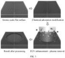
FIG. 3 is a flowchart of EUV-plasma enhancement removal process of Mode 3. - The present disclosure will be further described in detail below with reference to the accompanying drawings and specific embodiments. The following embodiments are only descriptive, not restrictive, and cannot limit the scope of the present disclosure.
- The key to improving the selectivity and controllability of atomic layer removal is to reduce the binding energy between atoms on a surface of the material, and further to control the action energy of the removal process to be between the surface binding energy and the bulk binding energy. According to this idea, three processing modes are proposed:
- The surface of the material is first irradiated with EUV light, and surface electrons absorb photons and are raised to a high-energy state. At the same time, the irradiation power and time are controlled to avoid large-scale atomic emission. In this case, the binding energy between the excited surface atoms is lower than the bulk binding energy inside the material. The activated atoms are removed by bombardment with plasma particles, and the incident energy of the ions is controlled so that the energy transmitted to the target atoms is between the excited state binding energy and the bulk binding energy of the surface layer of the material. Since the time scale of photoexcitation is on the order of femtoseconds to picoseconds, the EUV light source and the plasma beam can be turned on simultaneously. In this mode, EUV light is configured to reduce the surface atomic binding energy, plasma bombardment is configured for selective atomic layer removal, and large-scale atomic removal occurs only in a region where EUV light and plasma coexist. The removal process slows down significantly or even disappears under only one external field condition. The corresponding main steps are as follows (
FIG. 1 ): - (1) determining EUV exposure parameters.
- Assuming that the atomic binding energy per unit volume of the material to be processed is εG, the distance between the atomic layers corresponding to the processing surface is d, the number of atomic layers to be removed is N, and the atomic binding energy per unit volume in the activated state is εE , then the energy to be absorbed per unit area of the material surface is:

- When the irradiation power is P and the spot area is S, the corresponding irradiation time τ is:

- Based on the above initial values, the wavelength of the light source, the pulse width, and the properties of the material to be processed, a numerical simulation model is established, and the irradiation power and time are corrected by using the simulation results of molecular dynamics or quantum mechanics.
- (2) determining plasma bombardment parameters.
- Assuming that the number of chemical bonds in the unit volume of the material to be processed is n, the energy initial value Eion of the plasma incident particle is estimated as follows:

- Based on the above initial value range and plasma elements, molecular dynamics or quantum mechanics are used to simulate the ion bombardment process, and the energy, dose and beam intensity corresponding to the removal of only the activated atoms are determined.
- (3) pre-processing preparation.
- A sub-nanometer flat surface of the material to be processed is obtained by machining, polishing, chemical etching, heat treatment, etc.; the EUV light path and plasma beam are adjusted according to the parameters determined in steps (1) and (2), and alignment and synchronization of the two energy beams are completed (wherein a mask may be prepared according to specific processing needs); samples are placed, a coordinate system is established, and vacuuming is performed.
- (4) simultaneously turning on EUV beam and plasma beam for atomic layer removal processing.
- (5) measuring and evaluating a machining result.
- The highly chemically active plasma particles are firstly adsorbed on the surface of the material to change the electronic state of the extreme surface layer of the material and reduce the surface atomic binding energy; after the adsorption process is over, EUV light is irradiated, and the irradiation power and time are controlled to make the photon absorption energy per unit area is between the binding energy surface density and the bulk binding energy surface density of a modification region of the material atomic surface. Since the adsorbed particles generally only have a significant effect on the electronic state of a layer of substrate atoms in direct contact with the adsorbed particles, after the two energy fields act in succession (one processing cycle), theoretically, one atomic layer will be removed. Continuous layer-by-layer removal can be achieved through multiple cycles. The role of the plasma in this mode is to achieve surface modification by chemisorption, while the selective removal of atomic layers is achieved by EUV irradiation. The corresponding main steps are as follows (
FIG. 2 ): - (1) determining plasma surface modification parameters.
An atomic-level model of adsorption on the surface of the material is established, interatomic binding energies of the material before and after the adsorption of specific particles are obtained by quantum mechanics or molecular dynamics respectively to be EG-atomic and EM-atomic, and the influence law of temperature is obtained. According to the theoretical analysis results, the plasma elements, reaction temperature and time are determined. - (2) determining EUV exposure parameters.
- The binding energies that need to be overcome to remove the original and modified materials per unit area and thickness of a single atomic layer are about ndEG-atomic and ndEM-atomic, respectively, and the initial values of irradiation time and power for a single processing cycle may be estimated by the following equations:

- A numerical simulation model is established based on the above-mentioned initial value range, the wavelength of the light source, the pulse width, and the properties of the material to be processed, and the irradiation power and time are corrected by using the simulation results of molecular dynamics or quantum mechanics.
- (3) pre-processing preparation.
- A sub-nanometer flat surface of the material to be processed is obtained by machining, polishing, chemical etching, heat treatment, etc.; the EUV light path is adjusted according to the parameters determined in step (2) (wherein a mask may be prepared according to specific processing needs); samples are placed, a coordinate system is established, and vacuuming is performed.
- (4) turning off the EUV beam, feeding in the plasma according to the parameters determined in step (1); and after the reaction is completed, turning off the plasma source and vacuuming is performed to remove excess reaction gas.
- (5) turning on the EUV beam for atomic layer removal process.
- (6) when multiple machining cycles are required, repeating steps (4) and (5) to a specified number of times.
- (7) removing excess adsorbed particles from the surface.
- (8) measuring and evaluating a machining result.
- The key to suppressing the lattice damage caused by plasma bombardment is to reduce the incident ion energy, which may be achieved when the surface atomic binding energy of the material can be further weakened and the difference between the atomic binding energy and the bulk binding energy can be increased on the basis of surface adsorption. The first step of this mode is surface adsorption modification (same as mode 2), and in the second step, EUV light is used for enhanced excitation, and low-energy plasma bombardment is used to achieve material removal. The parameters of EUV irradiation and incident ions are controlled to avoid large-scale atomic emission when the two act alone. In addition, the energy transferred by the incident ions to the target atoms is greater than the binding energy of the enhanced excited state on the surface of the material, while the energy of the combined action of the EUV and the incident ions is less than the bulk binding energy. In this way, large-scale atomic removal occurs only in a region where EUV light and plasma coexist, and the removal process is significantly slowed down or even disappears with only one external field condition. The corresponding main steps are as follows (
FIG. 3 ): - (1) determining plasma surface modification parameters, same as step (1) in Mode 2.
- (2) determining EUV irradiation parameters and plasma bombardment parameters.
- The initial values of irradiation time, power and incident ion energy for removing unit area and single atomic layer can be estimated by the following equations:

- Based on the above initial value range, the wavelength of the light source, the pulse width, the plasma elements, and the properties of the material to be processed, a numerical simulation model is established, and molecular dynamics or quantum mechanics are used to simulate the process of EUV irradiation and bombardment. The energy, dose and beam intensity are accurately calculated and corrected to ensure that under the final optimized parameters, no large-scale atomic emission occurs when EUV light and ion beam exist alone, and when the two work together, only the atomic layer modified in step (1) is removed.
- (3) pre-processing preparation, same as step (3) in Mode 1.
- (4) plasma surface modification, same as step (4) in Mode 2.
- (5) atomic layer processing, same as step (4) in Mode 1.
- (6) when multiple machining cycles are required, repeating steps (4) and (5) to a specified number of times.
- (7) removing excess adsorbed particles from the surface.
- (8) measuring and evaluating a machining result.
- The following is an example of atomic layer removal on the surface of single crystal silicon using mode 3. The specific steps are as follows:
- 1. determining plasma surface modification parameters.
- 2. determining EUV irradiation parameters and plasma bombardment parameters.
- 3. pre-processing preparation.
- 4. turning off the EUV beam, and feeding in the plasma according to the parameters determined in step 1; after the reaction is completed, turning off the plasma source and vacuuming is performed to remove excess reaction gas.
- 5. synchronously turning on the EUV beam and the plasma beam, and performing the atomic layer removal processing according to the parameters determined in step 2.
- 6. when multiple machining cycles are required, repeating steps 4 and 5 to a specified number of times.
- 7. removing excess adsorbed particles from the surface.
- 8. measuring and evaluating a machining result.
- The plasma surface modification parameters mentioned in step 1 include plasma elements, reaction temperature and time; in the process of parameter design, quantum mechanics or molecular dynamics calculations may be used to obtain the binding energy between atoms of the material before and after the adsorption of specific particles and the variation curve of the binding energy as a function of temperature.
- The EUV irradiation parameters mentioned in step 2 include wavelength, pulse width, beam spot area, power and irradiation time; plasma bombardment parameters include incident ion element, energy, dose and beam intensity; in the parameter design process, quantum mechanics or molecular dynamics may be used to simulate the process of EUV irradiation and bombardment to ensure that under the final optimized parameters, no large-scale atomic emission occurs when EUV light and ion beam exist alone, and when the two act together, only the atomic layer modified in step (1) is removed.
- The preliminary preparation mentioned in step 3 includes the use of machining, polishing, chemical etching, heat treatment and other methods to obtain a sub-nanometer flat surface of the material to be processed (of which the roughness Sa is less than 1 nm); according to the parameters determined in steps 1 and 2, the EUV path and plasma beam flow are determined, and the alignment and synchronization of the two energy beams are completed (wherein a mask may be prepared according to specific processing needs); samples are placed, a coordinate system is established, and vacuuming is performed (<2×10⁻⁴Pa).
- The measurement methods mentioned in step 7 include STM, STEM, and AFM, and the evaluation indicators include atomic-scale material removal, surface roughness, and lattice deformation layer thickness.
- The above are only the preferred embodiments of the present disclosure. It should be noted that for those skilled in the art, without departing from the inventive concept, several modifications and improvements can be made, which are within the scope of the present disclosure.
Claims (8)
- An extreme ultraviolet light and plasma composite atomic-scale processing method, comprising:
synergistically applying extreme ultraviolet (EUV) light and plasma to treat a surface of a material, enabling atomic-scale processing of the surface of the material. - The method according to claim 1, wherein the surface of the material is first irradiated with the EUV light so that a bonding energy between excited surface atoms is less than a bulk bonding energy inside the material, and the excited surface atoms are removed by bombardment with plasma particles.
- The method according to claim 2, wherein an incident ion energy is controlled so that an energy delivered to target atoms is between the binding energy and the bulk binding energy of the surface of the material in an excited state.
- The method according to claim 1, wherein highly chemically active plasma particles are first adsorbed on the surface of the material to reduce an atomic binding energy, and an irradiation with the EUV light is performed.
- The method according to claim 4, wherein power and time of the irradiation with the EUV light are controlled so that a photon absorption energy per unit area is between a binding energy surface density and a bulk binding energy surface density in an atomic modified region of the surface of the material.
- The method according to claim 1, wherein highly chemically active plasma particles are first adsorbed on the surface of the material to reduce an atomic binding energy, and an irradiation with the EUV light and a low-energy plasma bombardment are performed simultaneously.
- The method according to claim 6, wherein power and time of irradiation with the EUV light as well as an ion incident energy are controlled, so that an energy when each of the EUV light and the plasma acting alone is less than the atomic binding energy of the adsorbed-modified surface, and a total energy when the EUV light and the plasma acting together is between the atomic binding energy and a bulk binding energy of the adsorbed-modified surface.
- The method according to any one of claims 1-7, wherein the surface of the material is treated to a sub-nanometer flat surface prior to processing.
Applications Claiming Priority (2)
| Application Number | Priority Date | Filing Date | Title |
|---|---|---|---|
| CN202010804942.0A CN111994868B (en) | 2020-08-12 | 2020-08-12 | Extreme ultraviolet light and plasma composite atomic scale processing method |
| PCT/CN2020/131669 WO2022032931A1 (en) | 2020-08-12 | 2020-11-26 | Extreme ultraviolet light and plasma combined atomic-scale processing method |
Publications (2)
| Publication Number | Publication Date |
|---|---|
| EP4197966A1 true EP4197966A1 (en) | 2023-06-21 |
| EP4197966A4 EP4197966A4 (en) | 2024-09-18 |
Family
ID=73463114
Family Applications (1)
| Application Number | Title | Priority Date | Filing Date |
|---|---|---|---|
| EP20949424.4A Pending EP4197966A4 (en) | 2020-08-12 | 2020-11-26 | ATOMIC SCALE TREATMENT PROCESS COMBINED BY EXTREME ULTRAVIOLET LIGHT AND PLASMA |
Country Status (5)
| Country | Link |
|---|---|
| US (1) | US11600465B2 (en) |
| EP (1) | EP4197966A4 (en) |
| JP (1) | JP7398843B2 (en) |
| CN (1) | CN111994868B (en) |
| WO (1) | WO2022032931A1 (en) |
Families Citing this family (2)
| Publication number | Priority date | Publication date | Assignee | Title |
|---|---|---|---|---|
| WO2022046429A1 (en) * | 2020-08-27 | 2022-03-03 | Lam Research Corporation | Subtractive copper etch |
| CN117800285B (en) * | 2024-03-01 | 2024-05-17 | 浙江大学 | A multi-energy field induced atomic-level numerical control processing device and method under ambient atmosphere |
Family Cites Families (28)
| Publication number | Priority date | Publication date | Assignee | Title |
|---|---|---|---|---|
| JPH0691048B2 (en) * | 1985-05-17 | 1994-11-14 | 日本真空技術株式会社 | Substrate dry processing method and apparatus |
| JPS63208221A (en) * | 1987-02-25 | 1988-08-29 | Hitachi Ltd | plasma processing equipment |
| JP3357951B2 (en) * | 1991-01-18 | 2002-12-16 | ▲靖▼浩 堀池 | Dry etching method |
| JPH05102101A (en) * | 1991-02-15 | 1993-04-23 | Fujitsu Ltd | Manufacture of semiconductor device |
| JP2920850B2 (en) * | 1991-03-25 | 1999-07-19 | 東京エレクトロン株式会社 | Semiconductor surface treatment method and apparatus |
| JP2001176860A (en) | 1999-12-20 | 2001-06-29 | Sony Corp | Semiconductor device manufacturing method and semiconductor manufacturing apparatus |
| CN2550376Y (en) * | 2002-06-20 | 2003-05-14 | 复旦大学 | Multifunction device for plasma and laser beam combined treatment material |
| CN1473952A (en) * | 2003-07-24 | 2004-02-11 | 复旦大学 | A Method of Combining Microwave Plasma and Laser to Treat Material Surface at Normal Temperature |
| US7964039B2 (en) * | 2007-09-07 | 2011-06-21 | Imec | Cleaning of plasma chamber walls using noble gas cleaning step |
| JP2009152081A (en) * | 2007-12-20 | 2009-07-09 | Panasonic Electric Works Co Ltd | Plasma processing apparatus and plasma processing method |
| CN104716007A (en) * | 2013-12-13 | 2015-06-17 | 中国科学院大连化学物理研究所 | Combined ionization source based on vacuum ultraviolet lamp and discharge ionization |
| US9564286B2 (en) * | 2014-08-14 | 2017-02-07 | Samsung Electronics Co., Ltd. | Method of forming thin film of semiconductor device |
| JP2016058590A (en) | 2014-09-11 | 2016-04-21 | 株式会社日立ハイテクノロジーズ | Plasma processing method |
| US9609730B2 (en) * | 2014-11-12 | 2017-03-28 | Lam Research Corporation | Adjustment of VUV emission of a plasma via collisional resonant energy transfer to an energy absorber gas |
| US9431268B2 (en) * | 2015-01-05 | 2016-08-30 | Lam Research Corporation | Isotropic atomic layer etch for silicon and germanium oxides |
| US20170040170A1 (en) * | 2015-08-06 | 2017-02-09 | Lam Research Corporation | Systems and Methods for Separately Applying Charged Plasma Constituents and Ultraviolet Light in a Mixed Mode Processing Operation |
| US9706634B2 (en) * | 2015-08-07 | 2017-07-11 | Varian Semiconductor Equipment Associates, Inc | Apparatus and techniques to treat substrates using directional plasma and reactive gas |
| CN106877176B (en) * | 2015-12-11 | 2018-03-16 | 中国电力科学研究院 | A kind of mixed type laser triggering gap |
| KR20170122910A (en) * | 2016-04-27 | 2017-11-07 | 성균관대학교산학협력단 | Atomic layer ething method |
| CN106370645A (en) * | 2016-08-17 | 2017-02-01 | 华中科技大学 | Plasma apparatus for laser-induced discharge of liquid tin target |
| US10550003B2 (en) * | 2017-02-08 | 2020-02-04 | Northwestern University | Electronically abrupt borophene/organic lateral heterostructures and preparation thereof |
| DE102017211539A1 (en) * | 2017-07-06 | 2019-01-10 | Carl Zeiss Smt Gmbh | A method for removing a contamination layer by an atomic layer etching process |
| CN109841493A (en) * | 2017-11-29 | 2019-06-04 | 中国科学院大连化学物理研究所 | A kind of VUV lamp ionization source device continuously monitored on-line for mass spectrum |
| CN109904056B (en) * | 2017-12-11 | 2020-05-08 | 中国科学院大连化学物理研究所 | A chemical ionization-vacuum ultraviolet single-photon ionization composite ionization source device based on air discharge |
| KR20190085654A (en) * | 2018-01-11 | 2019-07-19 | 삼성전자주식회사 | Method for manufacturing semiconductor device |
| CN110491754B (en) * | 2019-08-15 | 2020-08-07 | 中国科学院长春光学精密机械与物理研究所 | Optical processing device based on inductively coupled plasma and ion beam coupling |
| CN110880446B (en) * | 2019-11-26 | 2022-06-03 | 中国科学院合肥物质科学研究院 | Deep ultraviolet LED ionization source and working method thereof |
| CN111463122B (en) * | 2020-04-20 | 2021-04-20 | 天津大学 | Atomic-scale material controllable removal method based on extreme ultraviolet light |
-
2020
- 2020-08-12 CN CN202010804942.0A patent/CN111994868B/en active Active
- 2020-11-26 WO PCT/CN2020/131669 patent/WO2022032931A1/en not_active Ceased
- 2020-11-26 EP EP20949424.4A patent/EP4197966A4/en active Pending
- 2020-11-26 JP JP2022542889A patent/JP7398843B2/en active Active
-
2022
- 2022-06-30 US US17/854,112 patent/US11600465B2/en active Active
Also Published As
| Publication number | Publication date |
|---|---|
| CN111994868A (en) | 2020-11-27 |
| WO2022032931A1 (en) | 2022-02-17 |
| US11600465B2 (en) | 2023-03-07 |
| CN111994868B (en) | 2022-05-17 |
| EP4197966A4 (en) | 2024-09-18 |
| JP2023511859A (en) | 2023-03-23 |
| US20220336189A1 (en) | 2022-10-20 |
| JP7398843B2 (en) | 2023-12-15 |
Similar Documents
| Publication | Publication Date | Title |
|---|---|---|
| US11600465B2 (en) | Atomic-scale processing method by combining extreme ultraviolet light and plasma | |
| Jeschke et al. | Theory for the ultrafast ablation of graphite films | |
| Saeki et al. | Study on Radiation-Induced Reaction in Microscopic Region for Basic Understanding of Electron Beam Patterning in Lithographic Process (II)–Relation between Resist Space Resolution and Space Distribution of Ionic Species– | |
| Hosono | Importance of Implantation Sequence in the Formation of Nanometer Size Colloid Particles Embedded in Amorphous Si O 2: Formation of Composite Colloids with Cu Core and a Cu 2 O Shell by Coimplantation of Cu and F | |
| Sharopov et al. | Controlling the low-temperature ionic purification of a silicon surface by electron spectroscopy | |
| Yitzhak et al. | Evidence of structural changes in ion-irradiated graphene independent of the incident ions mass | |
| Iveković et al. | Suspended nanoporous graphene produced by swift heavy ion bombardment | |
| Sharopov | Surface Defects in Wide-Bandgap LiF, SiO2, and ZnO Crystals: Experiments and Simulations | |
| Cao et al. | Athermal repair of nanoscale defects in optical materials using a femtosecond laser | |
| Iwamura et al. | Increase of reaction products in deuterium permeation-induced transmutation | |
| Kharisov et al. | Main ionizing radiation types and their interaction with matter | |
| Baubekova et al. | Accumulation of oxygen interstitial-vacancy pairs under irradiation of corundum single crystals with energetic xenon ions | |
| Femi-Oyetoro et al. | Effects of high-dosage focused electron-beam irradiation at energies≤ 30 keV on graphene on SiO2 | |
| CN118026087A (en) | A micro-nano structure processing method | |
| Sergeev et al. | Electron-beam-induced absorption in quartz glasses | |
| Fescenko et al. | G-layers of NV Centers in Nitrogen-rich Diamonds | |
| Perinsky et al. | Ion-Beam-Assisted Formation of the Silver-Containing Surface of Porous Silicon | |
| Karlušić et al. | Materials modification using ions with energies below 1 MeV/u | |
| CN118748862A (en) | A method for increasing the intensity of extreme ultraviolet radiation using ceramic gadolinium target | |
| Nekita et al. | Carrier-mediated reduction mechanism in WO3 nanowires under electron-beam irradiation | |
| Zhang et al. | Modification of materials by MeV ion beams | |
| Gudimetla | system~ Ag~ X'~ Zo. | |
| Elcock | Characterization of Ion Implanted Materials for Photonic Applications: Radiation Damage in Tellurium Dioxide and Silicon LEDs | |
| Peng et al. | Femtosecond laser-induced damage in dielectrics | |
| Fuochi | Use of ionizing radiation for and in the electronic industry |
Legal Events
| Date | Code | Title | Description |
|---|---|---|---|
| STAA | Information on the status of an ep patent application or granted ep patent |
Free format text: STATUS: THE INTERNATIONAL PUBLICATION HAS BEEN MADE |
|
| PUAI | Public reference made under article 153(3) epc to a published international application that has entered the european phase |
Free format text: ORIGINAL CODE: 0009012 |
|
| STAA | Information on the status of an ep patent application or granted ep patent |
Free format text: STATUS: REQUEST FOR EXAMINATION WAS MADE |
|
| 17P | Request for examination filed |
Effective date: 20230313 |
|
| AK | Designated contracting states |
Kind code of ref document: A1 Designated state(s): AL AT BE BG CH CY CZ DE DK EE ES FI FR GB GR HR HU IE IS IT LI LT LU LV MC MK MT NL NO PL PT RO RS SE SI SK SM TR |
|
| DAV | Request for validation of the european patent (deleted) | ||
| DAX | Request for extension of the european patent (deleted) | ||
| A4 | Supplementary search report drawn up and despatched |
Effective date: 20240820 |
|
| RIC1 | Information provided on ipc code assigned before grant |
Ipc: H01J 37/32 20060101ALI20240813BHEP Ipc: B82Y 40/00 20110101ALI20240813BHEP Ipc: B82B 3/00 20060101AFI20240813BHEP |