EP4195262A1 - Semiconductor structure - Google Patents
Semiconductor structure Download PDFInfo
- Publication number
- EP4195262A1 EP4195262A1 EP21870914.5A EP21870914A EP4195262A1 EP 4195262 A1 EP4195262 A1 EP 4195262A1 EP 21870914 A EP21870914 A EP 21870914A EP 4195262 A1 EP4195262 A1 EP 4195262A1
- Authority
- EP
- European Patent Office
- Prior art keywords
- capacitor array
- conductive plug
- semiconductor structure
- koz
- capacitor
- Prior art date
- Legal status (The legal status is an assumption and is not a legal conclusion. Google has not performed a legal analysis and makes no representation as to the accuracy of the status listed.)
- Granted
Links
Images




Classifications
-
- H—ELECTRICITY
- H10—SEMICONDUCTOR DEVICES; ELECTRIC SOLID-STATE DEVICES NOT OTHERWISE PROVIDED FOR
- H10W—GENERIC PACKAGES, INTERCONNECTIONS, CONNECTORS OR OTHER CONSTRUCTIONAL DETAILS OF DEVICES COVERED BY CLASS H10
- H10W20/00—Interconnections in chips, wafers or substrates
- H10W20/40—Interconnections external to wafers or substrates, e.g. back-end-of-line [BEOL] metallisations or vias connecting to gate electrodes
- H10W20/495—Capacitive arrangements or effects of, or between wiring layers
-
- H—ELECTRICITY
- H10—SEMICONDUCTOR DEVICES; ELECTRIC SOLID-STATE DEVICES NOT OTHERWISE PROVIDED FOR
- H10W—GENERIC PACKAGES, INTERCONNECTIONS, CONNECTORS OR OTHER CONSTRUCTIONAL DETAILS OF DEVICES COVERED BY CLASS H10
- H10W20/00—Interconnections in chips, wafers or substrates
- H10W20/40—Interconnections external to wafers or substrates, e.g. back-end-of-line [BEOL] metallisations or vias connecting to gate electrodes
- H10W20/495—Capacitive arrangements or effects of, or between wiring layers
- H10W20/496—Capacitor integral with wiring layers
-
- H—ELECTRICITY
- H10—SEMICONDUCTOR DEVICES; ELECTRIC SOLID-STATE DEVICES NOT OTHERWISE PROVIDED FOR
- H10D—INORGANIC ELECTRIC SEMICONDUCTOR DEVICES
- H10D1/00—Resistors, capacitors or inductors
- H10D1/60—Capacitors
- H10D1/68—Capacitors having no potential barriers
-
- H—ELECTRICITY
- H10—SEMICONDUCTOR DEVICES; ELECTRIC SOLID-STATE DEVICES NOT OTHERWISE PROVIDED FOR
- H10W—GENERIC PACKAGES, INTERCONNECTIONS, CONNECTORS OR OTHER CONSTRUCTIONAL DETAILS OF DEVICES COVERED BY CLASS H10
- H10W20/00—Interconnections in chips, wafers or substrates
- H10W20/20—Interconnections within wafers or substrates, e.g. through-silicon vias [TSV]
-
- H—ELECTRICITY
- H10—SEMICONDUCTOR DEVICES; ELECTRIC SOLID-STATE DEVICES NOT OTHERWISE PROVIDED FOR
- H10W—GENERIC PACKAGES, INTERCONNECTIONS, CONNECTORS OR OTHER CONSTRUCTIONAL DETAILS OF DEVICES COVERED BY CLASS H10
- H10W20/00—Interconnections in chips, wafers or substrates
- H10W20/20—Interconnections within wafers or substrates, e.g. through-silicon vias [TSV]
- H10W20/211—Through-semiconductor vias, e.g. TSVs
- H10W20/213—Cross-sectional shapes or dispositions
- H10W20/2134—TSVs extending from the semiconductor wafer into back-end-of-line layers
-
- H—ELECTRICITY
- H10—SEMICONDUCTOR DEVICES; ELECTRIC SOLID-STATE DEVICES NOT OTHERWISE PROVIDED FOR
- H10W—GENERIC PACKAGES, INTERCONNECTIONS, CONNECTORS OR OTHER CONSTRUCTIONAL DETAILS OF DEVICES COVERED BY CLASS H10
- H10W20/00—Interconnections in chips, wafers or substrates
- H10W20/40—Interconnections external to wafers or substrates, e.g. back-end-of-line [BEOL] metallisations or vias connecting to gate electrodes
- H10W20/41—Interconnections external to wafers or substrates, e.g. back-end-of-line [BEOL] metallisations or vias connecting to gate electrodes characterised by their conductive parts
- H10W20/43—Layouts of interconnections
-
- H—ELECTRICITY
- H10—SEMICONDUCTOR DEVICES; ELECTRIC SOLID-STATE DEVICES NOT OTHERWISE PROVIDED FOR
- H10W—GENERIC PACKAGES, INTERCONNECTIONS, CONNECTORS OR OTHER CONSTRUCTIONAL DETAILS OF DEVICES COVERED BY CLASS H10
- H10W42/00—Arrangements for protection of devices
- H10W42/121—Arrangements for protection of devices protecting against mechanical damage
-
- H—ELECTRICITY
- H10—SEMICONDUCTOR DEVICES; ELECTRIC SOLID-STATE DEVICES NOT OTHERWISE PROVIDED FOR
- H10D—INORGANIC ELECTRIC SEMICONDUCTOR DEVICES
- H10D89/00—Aspects of integrated devices not covered by groups H10D84/00 - H10D88/00
- H10D89/10—Integrated device layouts
-
- H—ELECTRICITY
- H10—SEMICONDUCTOR DEVICES; ELECTRIC SOLID-STATE DEVICES NOT OTHERWISE PROVIDED FOR
- H10W—GENERIC PACKAGES, INTERCONNECTIONS, CONNECTORS OR OTHER CONSTRUCTIONAL DETAILS OF DEVICES COVERED BY CLASS H10
- H10W20/00—Interconnections in chips, wafers or substrates
- H10W20/40—Interconnections external to wafers or substrates, e.g. back-end-of-line [BEOL] metallisations or vias connecting to gate electrodes
- H10W20/41—Interconnections external to wafers or substrates, e.g. back-end-of-line [BEOL] metallisations or vias connecting to gate electrodes characterised by their conductive parts
- H10W20/423—Shielding layers
Definitions
- An embodiment of the present application relates to the field of semiconductors, in particular to a semiconductor structure.
- TSV Through-Silicon Vias
- the TSV technology is to form through holes for connecting the upper side and the lower side of a wafer, and the through holes are filled with conductive materials to form an interconnection structure.
- the conductive materials include different types of metal materials.
- the arrangement of the interconnection structure will affect elements arranged on the surface of the silicon wafer and elements arranged in the dielectric layer on the silicon wafer.
- An embodiment of the present application provides a semiconductor structure, which is beneficial to reduce the influence of the deformation stress generated by a conductive plug on functional elements.
- the embodiment of the present application provides a semiconductor structure, which includes: a substrate and a dielectric layer arranged on the substrate; a conductive plug, a first portion of the conductive plug being arranged in the substrate, and a second portion of the conductive plug being arranged in the dielectric layer; and a capacitor array, the capacitor array at least surrounding the second portion of the conductive plug.
- the capacitor array is used as a deformation isolation structure, and more interfaces may be provided in the capacitor array.
- Each interface includes a contact interface between an upper electrode and a lower electrode.
- FIG. 1 is a schematic cross-sectional diagram of a semiconductor structure in the related art
- FIG. 2 is a top view of a semiconductor structure shown in FIG. 1 .
- the semiconductor structure includes: a substrate 10 and a dielectric layer 11 arranged on the substrate 10; and a conductive plug 12, in which the conductive plug 12 is arranged in the substrate 10 and the dielectric layer 11.
- the conductive plug 12 usually contains a metal material, and the metal material is prone to expand and contract when subjected to a thermal stress.
- a thermal expansion coefficient of the conductive plug 12 is different from a thermal expansion coefficient of the dielectric layer 11 and a thermal expansion coefficient of the substrate 10
- a stress concentration phenomenon may occur, which in turn causes the substrate 10 and the dielectric layer 11 to deform.
- the deformation of the substrate 10 and the dielectric layer 11 may affect the characteristics of the functional elements in the functional zone, and even cause structural damage to the semiconductor structure.
- the functional zone is a workable zone of the functional elements, and includes a surface of the substrate 10 and an interior of the dielectric layer 11.
- the functional elements on the surface of the substrate 10 are generally referred to as active areas.
- the stress that causes the substrate 10 and the dielectric layer 11 to deform may also come from the secondary stress caused by the deformation of other adjacent film layers.
- the compressive stress of the conductive plug 12 causes the substrate 10 to deform, and the deformed substrate 10 applies stress to the dielectric layer 11 due to the structural change thereof, which in turn causes the dielectric layer 11 to deform.
- a grounded isolation ring structure 13 is provided to shield part of the electric field of the conductive plug 12, so as to reduce the influence of the electric field of the conductive plug 12, but there is no method to solve or counteract the deformation of the substrate 10 and the dielectric layer 11.
- the functional elements are usually arranged outside a Keep Out Zone, KOZ, that is, the functional elements are arranged away from the conductive plug 12.
- KOZ Keep Out Zone
- a capacitor array surrounding the conductive plug is provided, so as to reduce the magnitude of the deformation stress passing through the capacitor array, and to ensure that the deformation stress has a small impact on the functional zone arranged on a side of the capacitor array away from the conductive plug, thereby ensuring that the functional elements in the functional zone may work effectively and that the semiconductor structure has good performance.
- the semiconductor structure includes: a substrate 20; a dielectric layer 21 arranged on the substrate 20; a conductive plug 22, in which a first portion of the conductive plug 22 is arranged in the substrate 20, and a second portion of the conductive plug 22 is arranged in the dielectric layer 21; and a capacitor array 24, in which the capacitor array 24 at least surrounds the second portion of the conductive plug 22.
- the capacitor array 24 is formed by a plurality of capacitor units 24a. In a direction parallel to a surface of the substrate 20 and away from the conductive plug 22, the capacitor array 24 has a plurality of interfaces. The interfaces will hinder the transmission of the deformation stress, that is, attenuate the deformation stress, so as to ensure that the deformation stress transmitted to the functional zone 202 is relatively small, and ensure that the functional elements in the functional zone 202 have good performance.
- each capacitor unit 24a includes a double-sided capacitor unit.
- the capacitor array 24 includes multiple double-sided capacitor units 24a which are successively arranged.
- the interface in the capacitor array 24 mainly refers to a contact interface between a lower electrode 24b and an upper electrode 24c.
- each capacitor unit includes a single-sided capacitor unit.
- the capacitor array may include multiple capacitor units spaced apart from each other, and the interfaces in the capacitor array also include the side wall surfaces of the capacitor units.
- the substrate 20 includes a KOZ 201 and a functional zone 202.
- the functional zone 202 is arranged on a side of the KOZ 201 away from the conductive plug 22.
- Each of the KOZ 201 and the functional zone 202 is provided with the capacitor array 24, and the capacitor array 24 in the KOZ 201 surrounds the second portion of the conductive plug 22.
- the capacitor array 24 in the KOZ 201 is referred to as a first capacitor array 241
- the capacitor array 24 in the functional zone 202 is referred to as a second capacitor array 242.
- the substrate 20 is provided with an active area 203 in the KOZ 201, and the first capacitor array 241 is electrically connected to the active area 203 in the KOZ 201.
- the first capacitor array 241 may be actuated through the active area 203, so that the first capacitor array 241 may be used as a backup capacitor and put into use during fuse repair.
- the KOZ 201 is also provided with a capacitor contact window 24d for connecting the active area 203 and the first capacitor array 241 with each other, and necessary bit lines (not shown), word lines (not shown), or other structures. That is, the electrical structure of the KOZ 201 may be exactly the same as the electrical structure of the functional zone 202. The difference between the electrical structure of the KOZ 201 and the electrical structure of the functional zone 202 is only that the positions of the KOZ 201 and the functional zone 202 are different from each other, and the electrical structure of the KOZ 201 is not put into use before fuse repair.
- the substrate 20 is also provided with an isolation structure 204 for isolating two adjacent active areas 203 from one another. Since the first capacitor array 241 includes a plurality of capacitor units 24a, the first capacitor array 241 corresponds to a plurality of active areas 203 and a plurality of isolation structures 204. The existence of the plurality of isolation structures 204 may increase the transmission attenuation of the deformation stress in the substrate 20, so as to avoid the deformation stress from passing through the substrate 20 to cause a relatively large impact on the functional elements in the dielectric layer 21.
- a pattern of the first capacitor array 241 is the same as a pattern of the second capacitor array 242.
- the first capacitor array 241 and the second capacitor array 242 may be formed through the same manufacturing process, which is beneficial to reduce the difficulty of the manufacture of the semiconductor structure.
- the capacitor array 24 at the edge of the structure when the capacitor array 24 is used to surround the conductive plug 22, the capacitor array 24 at the edge of the structure, which is formed through the same manufacturing process, is selected as the capacitor array 24 surrounding the conductive plug 22. Since the capacitor array 24 at the edge of the structure is easily affected by the edge effect of the structure during the formation, for example, among the multiple trenches formed by etching through a same mask, the top openings of the trenches at the edge of the structure are relatively small, the data storage performance of the capacitor array 24 at the edge of the structure may be relatively poor.
- the capacitor array 24 is used as a transitional high-density functional element arranged in the KOZ 201, which is beneficial to realize the function of the capacitor array 24 at the edge of the structure and avoid the capacitor array 24 at the edge of the structure from occupying the space in the functional zone 202, so that more capacitor arrays 24 with good performance are provided in the functional zone 202 to improve the performance of the semiconductor structure.
- the reserved space region for the conductive plug may be embedded in the entire region of the capacitor array.
- the capacitor array which is close to and surrounds a partial region of the reserved space region is easily affected by the conductive plug.
- the partial region of reserved space region may be defined as a KOZ, and the capacitor array in the partial region of reserved space region may be defined as a backup capacitor.
- a first predetermined distance d1 is formed between the first capacitor array 241 and the second capacitor array 242.
- the existence of the first predetermined distance d1 is beneficial to avoid the first capacitor array 241 affected by the conductive plug 22 from affecting the second capacitor array 242, so as to ensure that the second capacitor array 242 has better performance.
- the influence of the first capacitor array 241 on the second capacitor array 242 includes potential influence and structural influence.
- the first capacitor array 241 is grounded, or the first capacitor array 241 is grounded through the active area 203, the capacitor contact window 24d, the word line or the bit line, so as to form an electrostatic shielding.
- the grounded first capacitor array 241 is at a low potential, and at least a portion of the capacitor units 24a in the second capacitor array 242 for data storage stores charges, that is, at least the portion of the capacitor units 24a are at a high level.
- the first predetermined distance d1 is used for isolation, which can effectively block the transfer path of the charges, thereby ensuring the accuracy and effectiveness of the data storage of the second capacitor array 242.
- the grounded first capacitor array 242 may be disconnected from a ground wire when it is subsequently put into use, so as to perform data storage.
- the upper electrode 24c of the current capacitor array 24 is usually a continuous film layer integrally formed, without an internal interface therein, the deformation stress can be transmitted through the upper electrode 24c with a relatively low transmission attenuation. In this way, continuous arrangement of the first capacitor array 241 and the second capacitor array 242 may cause the second capacitor array 242 to be more susceptible to the deformation stress. Electrodes of the capacitor array 24 are usually of a structure with a high height-to-width ratio, so that the electrodes are more sensitive to the deformation stress, and are prone to collapse when subjected to the deformation stress.
- the first predetermined distance d1 is set, so that the upper electrodes 24c of different capacitor arrays 24 may be spaced apart from each other, which is beneficial to ensure that the deformation stress to which the second capacitor array 242 is subjected is relatively small, and that the second capacitor array 242 has high structural stability.
- the first predetermined distance d1 is comprised between 0.2 ⁇ m and 20 ⁇ m, for example, 1 ⁇ m, 5 ⁇ m, or 10 ⁇ m. If the first predetermined distance d1 is too small, the first capacitor array 241 will affect the data storage accuracy and structural stability of the second capacitor array 242. If the first predetermined distance d1 is too large, the reserved space in the functional zone 202 may be compressed.
- the capacitor array 34 is a structure continuously integrally formed, and the first capacitor array 341 and the second capacitor array 342 are continuously arranged. In this way, the first capacitor array 341 and the second capacitor array 342 can be continuously formed by using the same mask, so as to reduce the difficulty of manufacture of the semiconductor structure.
- the second capacitor array 242 surrounds the second portion of the conductive plug 22, and the surrounding configuration of the first capacitor array 241 is different from the surrounding configuration of the second capacitor array 242.
- both the first capacitor array 241 and the second capacitor array 242 completely surround the conductive plug 22, but the surrounding configuration of the first capacitor array and the surrounding configuration of the second capacitor array are different from each other. In this way, the distances between the first capacitor array 241 and the second capacitor array 242 may be different in different directions away from the conductive plug 22. Further, the portion of the second capacitor array 242, which is more sensitive to the deformation stress, is arranged farther from the first capacitor array 241, so as to ensure that any portion of the second capacitor array 242 has high structural stability.
- the first capacitor array 241 may be in a circular shape, and the second capacitor array 242 may be in an elliptical shape. A part corresponding to an end point of the long axis of the ellipse is the portion of the second capacitor array 242 which is more sensitive to the deformation stress.
- the first capacitor array 241 is in a square shape, and the second capacitor array 242 is in a circular shape.
- the first capacitor array 241 is in a circular shape
- the second capacitor array 242 is in a polygonal shape, such as in a rhombus shape.
- the first capacitor array 241 does not completely surround the conductive plug 22, while the second capacitor array 242 completely surrounds the conductive plug 22.
- the first capacitor array 241 may be arranged in the partial region, so that the sensitive portion in the second capacitor array 242 can be protected, thereby ensuring that the whole second capacitor array 242 has high structural stability.
- the first capacitor array 241 may be in an arc shape, and the second capacitor array 242 may be in a circular shape.
- the first capacitor array 241 may be in a linear shape, and the second capacitor array 242 may be in a square shape.
- the semiconductor structure further includes an isolation ring structure 23.
- the isolation ring structure 23 at least surrounds the second portion of the conductive plug 22.
- the isolation ring structure 23 is arranged between the conductive plug 22 and the first capacitor array 241.
- An arrangement density of the first capacitor array 241 is greater than an arrangement density of the isolation ring structure 23. In this way, the functional elements with a relatively large arrangement density may be provided in the functional zone 202.
- the isolation ring structure 23 may be grounded.
- the first capacitor array 241 may not be grounded.
- the isolation ring structure 23 plays a role of electrostatic shielding, and the first capacitor array 241 plays a role of blocking the deformation stress. In this way, when the first capacitor array 241 is subsequently put into use, there is no need to disconnect the ground wire of the first capacitor array 241, which is beneficial to improve the applicability of the semiconductor structure.
- the isolation ring structure 23 may include a contact portion extending in the same direction as the conductive plug 22, and a metal portion arranged at the top of the contact portion.
- the capacitor array 44 includes a plurality of discontinuous capacitor sub-arrays.
- the isolation ring structure 43 includes a plurality of discontinuous isolation sub-rings. Each isolation sub-ring is arranged between two adjacent capacitor sub-arrays.
- the isolation ring structure 43 and the capacitor array 44 form a pattern surrounding the conductive plug 42.
- the pattern may be in any shape, such as a square shape, a circular shape, an elliptical shape, or a polygon shape.
- the isolation ring structure 43 is electrically isolated from the capacitor array 44.
- the isolation ring structure 43 is grounded to play a role of electrostatic shielding, and the capacitor array 44 is not grounded to play a role of blocking the deformation stress.
- the capacitor array 54 including a plurality of capacitor sub-arrays constitutes a first pattern surrounding the conductive plug 52
- the isolation ring structure 53 including a plurality of isolation sub-rings constitutes a second pattern surrounding the conductive plug 52.
- the first pattern and the second pattern have the same shape but are at different positions.
- an orthographic projection of the second pattern may be complementary to the first pattern, so as to constitute a complete enclosed pattern.
- the shape of the first pattern and the shape of the second pattern may also be different from each other, and the orthographic projection of the second pattern may also partially overlap with the first pattern, or there may be a gap between the orthographic projection of the second pattern and the first pattern.
- a second predetermined distance d2 is formed between the conductive plug 22 and the first capacitor array 241.
- the second predetermined distance d2 is comprised between 0.5 ⁇ m to 50 ⁇ m, for example, 2 ⁇ m, 10 ⁇ m or 25 ⁇ m. If the second predetermined distance d2 is too small, the first capacitor array 241 is easily damaged by the deformation stress of the conductive plug 22, so that the first capacitor array 241 cannot achieve the effect of deformation isolation, and the first capacitor array 241 cannot be used as a backup capacitor. If the second predetermined distance d2 is too large, the reserved space in the functional zone 202 may be compressed.
- a top surface of the second portion of the conductive plug 22 is lower than or flush with a top surface of the first capacitor array 241.
- the deformation stress generated by the conductive plug 22 to be applied to the dielectric layer 21 must pass through the interfaces in the first capacitor array 241 or bypass the first capacitor array 241, instead of directly affecting the active area 203 on the surface of the substrate 20 or the functional element in the dielectric layer 21. That is, the deformation stress transmitted to the functional elements or the active area 203 is reduced, thereby ensuring that each of the functional elements or the active area 203 has good performance.
- the capacitor array is used as a deformation isolation structure, and more interfaces may be provided in the capacitor array.
- Each interface includes a contact interface between the upper electrode and the lower electrode.
- the embodiment of the present application provides a semiconductor structure, which includes: a substrate; a dielectric layer arranged on the substrate; a conductive plug, a first portion of the conductive plug being arranged in the substrate, and a second portion of the conductive plug being arranged in the dielectric layer; and a capacitor array, the capacitor array at least surrounding the second portion of the conductive plug.
- the embodiment of the present application is beneficial to reduce the influence of the deformation stress generated by the conductive plug on the functional elements.
Landscapes
- Semiconductor Integrated Circuits (AREA)
- Engineering & Computer Science (AREA)
- Power Engineering (AREA)
- Internal Circuitry In Semiconductor Integrated Circuit Devices (AREA)
Abstract
Description
- The application claims priority to
Chinese Patent Application No. 202011013111.8, filed on September 23, 2020 - An embodiment of the present application relates to the field of semiconductors, in particular to a semiconductor structure.
- In order to realize the integration and assembly of chips in a Z-axis direction, interconnection between the chips is usually realized through a Through-Silicon Vias, TSV, technology. Specifically, the TSV technology is to form through holes for connecting the upper side and the lower side of a wafer, and the through holes are filled with conductive materials to form an interconnection structure. The conductive materials include different types of metal materials.
- However, in an actual application process, the arrangement of the interconnection structure will affect elements arranged on the surface of the silicon wafer and elements arranged in the dielectric layer on the silicon wafer.
- An embodiment of the present application provides a semiconductor structure, which is beneficial to reduce the influence of the deformation stress generated by a conductive plug on functional elements.
- The embodiment of the present application provides a semiconductor structure, which includes: a substrate and a dielectric layer arranged on the substrate; a conductive plug, a first portion of the conductive plug being arranged in the substrate, and a second portion of the conductive plug being arranged in the dielectric layer; and a capacitor array, the capacitor array at least surrounding the second portion of the conductive plug.
- The technical solution provided by the embodiment of the present application has the following advantages.
- The capacitor array is used as a deformation isolation structure, and more interfaces may be provided in the capacitor array. Each interface includes a contact interface between an upper electrode and a lower electrode. When the deformation stress is transmitted in the capacitor array, the deformation stress needs to continuously pass through the interfaces or bypass the interfaces, so that relatively high transmission attenuation will be generated. In this way, it is beneficial to ensure that the deformation stress has a small impact on the functional elements arranged on a side of the capacitor array away from the conductive plug, thereby ensuring that the semiconductor structure has good performance.
- One or more embodiments are exemplarily explained through the figures in accompanying drawings corresponding thereto, these exemplary explanations do not constitute a limitation to the embodiments, elements having the same reference numerals in the accompanying drawings are denoted as similar elements; and unless otherwise specifically declared, the figures in the accompanying drawings do not constitute a limitation of proportion.
-
FIG. 1 is a schematic cross-sectional diagram of a semiconductor structure in the related art; -
FIG. 2 is a top view of a semiconductor structure shown inFIG. 1 ; -
FIG. 3 is a schematic cross-sectional diagram of a semiconductor structure according to an embodiment of the present application; -
FIG. 4 is a top view of a semiconductor structure shown inFIG. 3 ; -
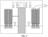
FIG. 5 is a schematic cross-sectional diagram of another semiconductor structure according to an embodiment of the present application; -
FIG. 6 is a top view of a semiconductor structure shown inFIG. 5 ; -
FIG. 7 is a top view of yet another semiconductor structure according to an embodiment of the present application; and -
FIG. 8 is a top view of a still further semiconductor structure according to an embodiment of the present application. - 10, 20: substrate; 11, 21: dielectric layer; 12, 22, 42, 52: conductive plug; 13, 23, 43, 53: isolation ring structure; 201, KOZ: Keep Out Zone; 202: functional zone; 203: active area; 204: isolation structure; 24, 34, 44, 54: capacitor array; 24a: capacitor unit; 24b: lower electrode; 24c: upper electrode; 24d: capacitor contact window; 241, 341: first capacitor array; 242, 342: second capacitor array.
- With reference to
FIG. 1 and FIG. 2, FIG. 1 is a schematic cross-sectional diagram of a semiconductor structure in the related art, andFIG. 2 is a top view of a semiconductor structure shown inFIG. 1 . The semiconductor structure includes: asubstrate 10 and adielectric layer 11 arranged on thesubstrate 10; and aconductive plug 12, in which theconductive plug 12 is arranged in thesubstrate 10 and thedielectric layer 11. - The
conductive plug 12 usually contains a metal material, and the metal material is prone to expand and contract when subjected to a thermal stress. When a thermal expansion coefficient of theconductive plug 12 is different from a thermal expansion coefficient of thedielectric layer 11 and a thermal expansion coefficient of thesubstrate 10, a stress concentration phenomenon may occur, which in turn causes thesubstrate 10 and thedielectric layer 11 to deform. The deformation of thesubstrate 10 and thedielectric layer 11 may affect the characteristics of the functional elements in the functional zone, and even cause structural damage to the semiconductor structure. - The functional zone is a workable zone of the functional elements, and includes a surface of the
substrate 10 and an interior of thedielectric layer 11. The functional elements on the surface of thesubstrate 10 are generally referred to as active areas. - It should be noted that in addition to the direct stress from the
conductive plug 12, the stress that causes thesubstrate 10 and thedielectric layer 11 to deform may also come from the secondary stress caused by the deformation of other adjacent film layers. For example, the compressive stress of theconductive plug 12 causes thesubstrate 10 to deform, and thedeformed substrate 10 applies stress to thedielectric layer 11 due to the structural change thereof, which in turn causes thedielectric layer 11 to deform. - At present, only a grounded
isolation ring structure 13 is provided to shield part of the electric field of theconductive plug 12, so as to reduce the influence of the electric field of theconductive plug 12, but there is no method to solve or counteract the deformation of thesubstrate 10 and thedielectric layer 11. In order to prevent the deformation of thesubstrate 10 and thedielectric layer 11 from affecting the functional elements in the functional zone, the functional elements are usually arranged outside a Keep Out Zone, KOZ, that is, the functional elements are arranged away from theconductive plug 12. However, such a solution will greatly compress the reserved space for the functional elements, which is not conducive to the integration of the chips or the functional elements. - According to a semiconductor structure provided in an embodiment of the present application, a capacitor array surrounding the conductive plug is provided, so as to reduce the magnitude of the deformation stress passing through the capacitor array, and to ensure that the deformation stress has a small impact on the functional zone arranged on a side of the capacitor array away from the conductive plug, thereby ensuring that the functional elements in the functional zone may work effectively and that the semiconductor structure has good performance.
- In order to make the objectives, technical solutions and advantages of the embodiments of the present application more apparent, hereinafter, the respective embodiments of the present application will be described in detail in connection with the accompanying drawings. However, those ordinary skilled in the art may understand that, in the respective embodiments of the present application, numerous technical details are set forth in order to provide a reader with a better understanding of the present application. However, the technical solutions claimed in the present application can also be implemented without these technical details and various changes and modifications based on the respective embodiments below.
- In the embodiment of the present application, with reference to
FIG. 3 andFIG. 4 , the semiconductor structure includes: asubstrate 20; adielectric layer 21 arranged on thesubstrate 20; aconductive plug 22, in which a first portion of theconductive plug 22 is arranged in thesubstrate 20, and a second portion of theconductive plug 22 is arranged in thedielectric layer 21; and acapacitor array 24, in which thecapacitor array 24 at least surrounds the second portion of theconductive plug 22. - The
capacitor array 24 is formed by a plurality ofcapacitor units 24a. In a direction parallel to a surface of thesubstrate 20 and away from theconductive plug 22, thecapacitor array 24 has a plurality of interfaces. The interfaces will hinder the transmission of the deformation stress, that is, attenuate the deformation stress, so as to ensure that the deformation stress transmitted to thefunctional zone 202 is relatively small, and ensure that the functional elements in thefunctional zone 202 have good performance. - In the embodiment of the present application, each
capacitor unit 24a includes a double-sided capacitor unit. Thecapacitor array 24 includes multiple double-sided capacitor units 24a which are successively arranged. The interface in thecapacitor array 24 mainly refers to a contact interface between alower electrode 24b and anupper electrode 24c. In some embodiments of the present application, each capacitor unit includes a single-sided capacitor unit. The capacitor array may include multiple capacitor units spaced apart from each other, and the interfaces in the capacitor array also include the side wall surfaces of the capacitor units. - In the embodiment of the present application, the
substrate 20 includes aKOZ 201 and afunctional zone 202. Thefunctional zone 202 is arranged on a side of theKOZ 201 away from theconductive plug 22. Each of theKOZ 201 and thefunctional zone 202 is provided with thecapacitor array 24, and thecapacitor array 24 in theKOZ 201 surrounds the second portion of theconductive plug 22. By setting thecapacitor array 24 at the edge of theKOZ 201 as a transition, a difference between an element arrangement density in theKOZ 201 and an element arrangement density in thefunctional zone 202 is prevented from being too large, so as to ensure that the functional elements with a relatively large element arrangement density can be provided in thefunctional zone 202, and to ensure that the functional elements in thefunctional zone 202 can work effectively. - It should be noted that in the structure shown in
FIG. 1 , the fact that only thecapacitor array 24 is provided in thefunctional zone 202 is taken as an example. In fact, any functional elements may be provided in thefunctional zone 202. In addition, hereinafter, for the sake of simplicity of description, thecapacitor array 24 in theKOZ 201 is referred to as afirst capacitor array 241, and thecapacitor array 24 in thefunctional zone 202 is referred to as asecond capacitor array 242. - In the embodiment of the present application, the
substrate 20 is provided with anactive area 203 in theKOZ 201, and thefirst capacitor array 241 is electrically connected to theactive area 203 in theKOZ 201. In this way, it is beneficial to ensure that thefirst capacitor array 241 may be actuated through theactive area 203, so that thefirst capacitor array 241 may be used as a backup capacitor and put into use during fuse repair. - In some embodiments of the present application, the
KOZ 201 is also provided with acapacitor contact window 24d for connecting theactive area 203 and thefirst capacitor array 241 with each other, and necessary bit lines (not shown), word lines (not shown), or other structures. That is, the electrical structure of theKOZ 201 may be exactly the same as the electrical structure of thefunctional zone 202. The difference between the electrical structure of theKOZ 201 and the electrical structure of thefunctional zone 202 is only that the positions of theKOZ 201 and thefunctional zone 202 are different from each other, and the electrical structure of theKOZ 201 is not put into use before fuse repair. - In some embodiments of the present application, in the
KOZ 201, thesubstrate 20 is also provided with anisolation structure 204 for isolating two adjacentactive areas 203 from one another. Since thefirst capacitor array 241 includes a plurality ofcapacitor units 24a, thefirst capacitor array 241 corresponds to a plurality ofactive areas 203 and a plurality ofisolation structures 204. The existence of the plurality ofisolation structures 204 may increase the transmission attenuation of the deformation stress in thesubstrate 20, so as to avoid the deformation stress from passing through thesubstrate 20 to cause a relatively large impact on the functional elements in thedielectric layer 21. - In the embodiment of the present application, a pattern of the
first capacitor array 241 is the same as a pattern of thesecond capacitor array 242. In this way, thefirst capacitor array 241 and thesecond capacitor array 242 may be formed through the same manufacturing process, which is beneficial to reduce the difficulty of the manufacture of the semiconductor structure. - In the embodiment of the present application, when the
capacitor array 24 is used to surround theconductive plug 22, thecapacitor array 24 at the edge of the structure, which is formed through the same manufacturing process, is selected as thecapacitor array 24 surrounding theconductive plug 22. Since thecapacitor array 24 at the edge of the structure is easily affected by the edge effect of the structure during the formation, for example, among the multiple trenches formed by etching through a same mask, the top openings of the trenches at the edge of the structure are relatively small, the data storage performance of thecapacitor array 24 at the edge of the structure may be relatively poor. - In the case where the data storage performance of the
capacitor array 24 at the edge of the structure may be relatively poor, thecapacitor array 24 is used as a transitional high-density functional element arranged in theKOZ 201, which is beneficial to realize the function of thecapacitor array 24 at the edge of the structure and avoid thecapacitor array 24 at the edge of the structure from occupying the space in thefunctional zone 202, so thatmore capacitor arrays 24 with good performance are provided in thefunctional zone 202 to improve the performance of the semiconductor structure. - In some embodiments of the present application, when a capacitor array is used to surround the conductive plug, the reserved space region for the conductive plug may be embedded in the entire region of the capacitor array. In this case, the capacitor array which is close to and surrounds a partial region of the reserved space region is easily affected by the conductive plug. The partial region of reserved space region may be defined as a KOZ, and the capacitor array in the partial region of reserved space region may be defined as a backup capacitor.
- In the embodiment of the present application, in a direction from the
KOZ 201 to thefunctional zone 202, a first predetermined distance d1 is formed between thefirst capacitor array 241 and thesecond capacitor array 242. The existence of the first predetermined distance d1 is beneficial to avoid thefirst capacitor array 241 affected by theconductive plug 22 from affecting thesecond capacitor array 242, so as to ensure that thesecond capacitor array 242 has better performance. - The influence of the
first capacitor array 241 on thesecond capacitor array 242 includes potential influence and structural influence. - For the potential influence: in the embodiment of the present application, in order to prevent the electric field of the
conductive plug 22 from affecting the performance of the functional elements in thefunctional zone 202, thefirst capacitor array 241 is grounded, or thefirst capacitor array 241 is grounded through theactive area 203, thecapacitor contact window 24d, the word line or the bit line, so as to form an electrostatic shielding. Correspondingly, the groundedfirst capacitor array 241 is at a low potential, and at least a portion of thecapacitor units 24a in thesecond capacitor array 242 for data storage stores charges, that is, at least the portion of thecapacitor units 24a are at a high level. In order to avoid charges from being transferred and leaking due to the potential difference, the first predetermined distance d1 is used for isolation, which can effectively block the transfer path of the charges, thereby ensuring the accuracy and effectiveness of the data storage of thesecond capacitor array 242. - The grounded
first capacitor array 242 may be disconnected from a ground wire when it is subsequently put into use, so as to perform data storage. - For structural influence: since the
upper electrode 24c of thecurrent capacitor array 24 is usually a continuous film layer integrally formed, without an internal interface therein, the deformation stress can be transmitted through theupper electrode 24c with a relatively low transmission attenuation. In this way, continuous arrangement of thefirst capacitor array 241 and thesecond capacitor array 242 may cause thesecond capacitor array 242 to be more susceptible to the deformation stress. Electrodes of thecapacitor array 24 are usually of a structure with a high height-to-width ratio, so that the electrodes are more sensitive to the deformation stress, and are prone to collapse when subjected to the deformation stress. Therefore, the first predetermined distance d1 is set, so that theupper electrodes 24c ofdifferent capacitor arrays 24 may be spaced apart from each other, which is beneficial to ensure that the deformation stress to which thesecond capacitor array 242 is subjected is relatively small, and that thesecond capacitor array 242 has high structural stability. - In the embodiment of the present application, the first predetermined distance d1 is comprised between 0.2 µm and 20 µm, for example, 1 µm, 5 µm, or 10 µm. If the first predetermined distance d1 is too small, the
first capacitor array 241 will affect the data storage accuracy and structural stability of thesecond capacitor array 242. If the first predetermined distance d1 is too large, the reserved space in thefunctional zone 202 may be compressed. - In other embodiments, with reference to
FIG. 5 andFIG. 6 , thecapacitor array 34 is a structure continuously integrally formed, and thefirst capacitor array 341 and thesecond capacitor array 342 are continuously arranged. In this way, thefirst capacitor array 341 and thesecond capacitor array 342 can be continuously formed by using the same mask, so as to reduce the difficulty of manufacture of the semiconductor structure. - In the embodiment of the present application, the
second capacitor array 242 surrounds the second portion of theconductive plug 22, and the surrounding configuration of thefirst capacitor array 241 is different from the surrounding configuration of thesecond capacitor array 242. - In some embodiments of the present application, both the
first capacitor array 241 and thesecond capacitor array 242 completely surround theconductive plug 22, but the surrounding configuration of the first capacitor array and the surrounding configuration of the second capacitor array are different from each other. In this way, the distances between thefirst capacitor array 241 and thesecond capacitor array 242 may be different in different directions away from theconductive plug 22. Further, the portion of thesecond capacitor array 242, which is more sensitive to the deformation stress, is arranged farther from thefirst capacitor array 241, so as to ensure that any portion of thesecond capacitor array 242 has high structural stability. - In some embodiments of the present application, the
first capacitor array 241 may be in a circular shape, and thesecond capacitor array 242 may be in an elliptical shape. A part corresponding to an end point of the long axis of the ellipse is the portion of thesecond capacitor array 242 which is more sensitive to the deformation stress. Alternatively, thefirst capacitor array 241 is in a square shape, and thesecond capacitor array 242 is in a circular shape. Alternatively, thefirst capacitor array 241 is in a circular shape, and thesecond capacitor array 242 is in a polygonal shape, such as in a rhombus shape. - In some embodiments of the present application, the
first capacitor array 241 does not completely surround theconductive plug 22, while thesecond capacitor array 242 completely surrounds theconductive plug 22. In this way, thefirst capacitor array 241 may be arranged in the partial region, so that the sensitive portion in thesecond capacitor array 242 can be protected, thereby ensuring that the wholesecond capacitor array 242 has high structural stability. - In some embodiments of the present application, the
first capacitor array 241 may be in an arc shape, and thesecond capacitor array 242 may be in a circular shape. Thefirst capacitor array 241 may be in a linear shape, and thesecond capacitor array 242 may be in a square shape. - In the embodiment of the present application, the semiconductor structure further includes an
isolation ring structure 23. Theisolation ring structure 23 at least surrounds the second portion of theconductive plug 22. Theisolation ring structure 23 is arranged between theconductive plug 22 and thefirst capacitor array 241. An arrangement density of thefirst capacitor array 241 is greater than an arrangement density of theisolation ring structure 23. In this way, the functional elements with a relatively large arrangement density may be provided in thefunctional zone 202. - In some embodiments of the present application, the
isolation ring structure 23 may be grounded. Thefirst capacitor array 241 may not be grounded. Theisolation ring structure 23 plays a role of electrostatic shielding, and thefirst capacitor array 241 plays a role of blocking the deformation stress. In this way, when thefirst capacitor array 241 is subsequently put into use, there is no need to disconnect the ground wire of thefirst capacitor array 241, which is beneficial to improve the applicability of the semiconductor structure. - The
isolation ring structure 23 may include a contact portion extending in the same direction as theconductive plug 22, and a metal portion arranged at the top of the contact portion. - In some embodiments of the present application, with reference to
FIG. 7 , thecapacitor array 44 includes a plurality of discontinuous capacitor sub-arrays. Theisolation ring structure 43 includes a plurality of discontinuous isolation sub-rings. Each isolation sub-ring is arranged between two adjacent capacitor sub-arrays. Theisolation ring structure 43 and thecapacitor array 44 form a pattern surrounding theconductive plug 42. The pattern may be in any shape, such as a square shape, a circular shape, an elliptical shape, or a polygon shape. - The
isolation ring structure 43 is electrically isolated from thecapacitor array 44. Theisolation ring structure 43 is grounded to play a role of electrostatic shielding, and thecapacitor array 44 is not grounded to play a role of blocking the deformation stress. - In some embodiments of the present application, with reference to
FIG. 8 , thecapacitor array 54 including a plurality of capacitor sub-arrays constitutes a first pattern surrounding theconductive plug 52, and theisolation ring structure 53 including a plurality of isolation sub-rings constitutes a second pattern surrounding theconductive plug 52. The first pattern and the second pattern have the same shape but are at different positions. In a direction from theconductive plug 52 to thecapacitor array 54, an orthographic projection of the second pattern may be complementary to the first pattern, so as to constitute a complete enclosed pattern. - In some embodiments of the present application, the shape of the first pattern and the shape of the second pattern may also be different from each other, and the orthographic projection of the second pattern may also partially overlap with the first pattern, or there may be a gap between the orthographic projection of the second pattern and the first pattern.
- In the embodiment of the present application, in a direction from the
conductive plug 22 to thefirst capacitor array 241, a second predetermined distance d2 is formed between theconductive plug 22 and thefirst capacitor array 241. The second predetermined distance d2 is comprised between 0.5 µm to 50 µm, for example, 2 µm, 10 µm or 25 µm. If the second predetermined distance d2 is too small, thefirst capacitor array 241 is easily damaged by the deformation stress of theconductive plug 22, so that thefirst capacitor array 241 cannot achieve the effect of deformation isolation, and thefirst capacitor array 241 cannot be used as a backup capacitor. If the second predetermined distance d2 is too large, the reserved space in thefunctional zone 202 may be compressed. - In the embodiment of the present application, in a direction perpendicular to a surface of the
substrate 20, a top surface of the second portion of theconductive plug 22 is lower than or flush with a top surface of thefirst capacitor array 241. In this way, it is beneficial that the deformation stress generated by theconductive plug 22 to be applied to thedielectric layer 21 must pass through the interfaces in thefirst capacitor array 241 or bypass thefirst capacitor array 241, instead of directly affecting theactive area 203 on the surface of thesubstrate 20 or the functional element in thedielectric layer 21. That is, the deformation stress transmitted to the functional elements or theactive area 203 is reduced, thereby ensuring that each of the functional elements or theactive area 203 has good performance. - In the embodiment of the present application, the capacitor array is used as a deformation isolation structure, and more interfaces may be provided in the capacitor array. Each interface includes a contact interface between the upper electrode and the lower electrode. When the deformation stress is transmitted in the capacitor array, the deformation stress needs to continuously pass through the interfaces or bypass the interfaces, so that relatively high transmission attenuation will be generated. In this way, it is beneficial to ensure that the deformation stress has a small impact on an element arranged on a side of the capacitor array away from the conductive plug, thereby ensuring that the semiconductor structure has good performance.
- Those of ordinary skill in the art may understand that the above embodiments are specific embodiments to implement the present application. In practical applications, various changes may be made in form and details without departing from the spirit and scope of the present application. Any person skilled in the art may make changes and modifications without departing from the spirit and scope of the present application. Therefore, the protection scope of the present application should be subject to the scope defined by the appended claims.
- The embodiment of the present application provides a semiconductor structure, which includes: a substrate; a dielectric layer arranged on the substrate; a conductive plug, a first portion of the conductive plug being arranged in the substrate, and a second portion of the conductive plug being arranged in the dielectric layer; and a capacitor array, the capacitor array at least surrounding the second portion of the conductive plug. The embodiment of the present application is beneficial to reduce the influence of the deformation stress generated by the conductive plug on the functional elements.
Claims (11)
- A semiconductor structure, comprising:a substrate and a dielectric layer arranged on the substrate;a conductive plug, a first portion of the conductive plug being arranged in the substrate, and a second portion of the conductive plug being arranged in the dielectric layer; anda capacitor array, the capacitor array at least surrounding the second portion of the conductive plug.
- The semiconductor structure of claim 1, wherein the substrate comprises a functional zone and a Keep Out Zone, KOZ, the functional zone is arranged on a side of the KOZ away from the conductive plug, each of the KOZ and the functional zone is provided with the capacitor array, and the capacitor array in the KOZ surrounds the second portion of the conductive plug.
- The semiconductor structure of claim 2, wherein the substrate comprises an active area in the KOZ, and the capacitor array in the KOZ is electrically connected to the active area in the KOZ.
- The semiconductor structure of claim 2, wherein a pattern of the capacitor array in the KOZ is the same as a pattern of the capacitor array in the functional zone.
- The semiconductor structure of claim 2, wherein in a direction from the KOZ to the functional zone, a predetermined distance is formed between the capacitor array in the KOZ and the capacitor array in the functional zone.
- The semiconductor structure of claim 2, wherein the capacitor array in the functional zone surrounds the second portion of the conductive plug, and a surrounding configuration of the capacitor array in the KOZ is different from a surrounding configuration of the capacitor array in the functional zone.
- The semiconductor structure of claim 1, further comprising an isolation ring structure, wherein the isolation ring structure at least surrounds the second portion of the conductive plug, and is arranged between the conductive plug and the capacitor array.
- The semiconductor structure of claim 1, wherein the capacitor array comprises a plurality of discontinuous capacitor sub-arrays, and wherein the semiconductor structure further comprises an isolation ring structure, the isolation ring structure comprising a plurality of discontinuous isolation sub-rings, each isolation sub-ring being arranged between two adjacent capacitor sub-arrays, the isolation ring structure and the capacitor array form a pattern surrounding the conductive plug, and the isolation ring structure and the capacitor array being electrically isolated from each other.
- The semiconductor structure of claim 1, wherein the capacitor array is grounded.
- The semiconductor structure of claim 1, wherein in a direction from the conductive plug to the capacitor array, a distance between the conductive plug and the capacitor array is comprised between 0.05 µm and 50 µm.
- The semiconductor structure of claim 1, wherein in a direction perpendicular to a surface of the substrate, a top surface of the second portion of the conductive plug is lower than or flush with a top surface of the capacitor array.
Applications Claiming Priority (2)
| Application Number | Priority Date | Filing Date | Title |
|---|---|---|---|
| CN202011013111.8A CN114256196A (en) | 2020-09-23 | 2020-09-23 | Semiconductor structure |
| PCT/CN2021/103321 WO2022062535A1 (en) | 2020-09-23 | 2021-06-29 | Semiconductor structure |
Publications (3)
| Publication Number | Publication Date |
|---|---|
| EP4195262A1 true EP4195262A1 (en) | 2023-06-14 |
| EP4195262A4 EP4195262A4 (en) | 2024-01-03 |
| EP4195262B1 EP4195262B1 (en) | 2024-11-20 |
Family
ID=80740787
Family Applications (1)
| Application Number | Title | Priority Date | Filing Date |
|---|---|---|---|
| EP21870914.5A Active EP4195262B1 (en) | 2020-09-23 | 2021-06-29 | Semiconductor structure |
Country Status (2)
| Country | Link |
|---|---|
| US (1) | US12068239B2 (en) |
| EP (1) | EP4195262B1 (en) |
Family Cites Families (13)
| Publication number | Priority date | Publication date | Assignee | Title |
|---|---|---|---|---|
| US6159818A (en) | 1999-09-02 | 2000-12-12 | Micron Technology, Inc. | Method of forming a container capacitor structure |
| US6720232B1 (en) | 2003-04-10 | 2004-04-13 | Taiwan Semiconductor Manufacturing Company | Method of fabricating an embedded DRAM for metal-insulator-metal (MIM) capacitor structure |
| US8148223B2 (en) | 2006-05-22 | 2012-04-03 | Taiwan Semiconductor Manufacturing Co., Ltd. | 1T MIM memory for embedded ram application in soc |
| US20080122032A1 (en) | 2006-08-16 | 2008-05-29 | Taiwan Semiconductor Manufacturing Co., Ltd. | Semiconductor devices with MIM-type decoupling capacitors and fabrication method thereof |
| US7821108B2 (en) * | 2008-07-04 | 2010-10-26 | Micron Technology, Inc. | Systems and methods for lowering interconnect capacitance through adjustment of relative signal levels |
| TWI366890B (en) * | 2008-12-31 | 2012-06-21 | Ind Tech Res Inst | Method of manufacturing through-silicon-via and through-silicon-via structure |
| CN101789390A (en) | 2009-01-23 | 2010-07-28 | 财团法人工业技术研究院 | Method for manufacturing silicon through hole and silicon through hole structure |
| US9245799B2 (en) * | 2012-05-31 | 2016-01-26 | Intel Deutschland Gmbh | Semiconductor device and method of manufacturing thereof |
| US9923101B2 (en) * | 2012-09-13 | 2018-03-20 | Taiwan Semiconductor Manufacturing Co., Ltd. | Semiconductor structure |
| KR102114340B1 (en) * | 2013-07-25 | 2020-05-22 | 삼성전자주식회사 | Integrated circuit device having through-silicon via structure and decoupling capacitor and method of manufacturing the same |
| US9397038B1 (en) * | 2015-02-27 | 2016-07-19 | Invensas Corporation | Microelectronic components with features wrapping around protrusions of conductive vias protruding from through-holes passing through substrates |
| JP2018098461A (en) | 2016-12-16 | 2018-06-21 | 富士通株式会社 | Semiconductor device, manufacturing method thereof, and laminated semiconductor device |
| KR102511200B1 (en) | 2018-06-27 | 2023-03-17 | 삼성전자주식회사 | Semiconductor device and method of forming the same |
-
2021
- 2021-06-29 EP EP21870914.5A patent/EP4195262B1/en active Active
- 2021-09-26 US US17/448,892 patent/US12068239B2/en active Active
Also Published As
| Publication number | Publication date |
|---|---|
| US20220093506A1 (en) | 2022-03-24 |
| EP4195262B1 (en) | 2024-11-20 |
| EP4195262A4 (en) | 2024-01-03 |
| US12068239B2 (en) | 2024-08-20 |
Similar Documents
| Publication | Publication Date | Title |
|---|---|---|
| JP3968745B2 (en) | Antifuse structure and method for forming the same | |
| US6359804B2 (en) | Static semiconductor memory cell formed in an n-well and p-well | |
| US20010045670A1 (en) | Semiconductor device | |
| TW202011564A (en) | Transient voltage suppressor | |
| KR0120917B1 (en) | Method for manufacturing a semiconductor device having a cylindrical electrode | |
| CN112133699B (en) | Active area structure and forming method thereof | |
| KR20010062681A (en) | Semiconductor apparatus including bypass capacitor having structure for making automatic design easy, and semiconductor apparatus layout method | |
| US8604557B2 (en) | Semiconductor memory device and method for manufacturing | |
| KR100366905B1 (en) | Semiconductor integrated circuit having thereon on-chip capacitors | |
| EP4195262B1 (en) | Semiconductor structure | |
| WO2022062535A1 (en) | Semiconductor structure | |
| US12495536B2 (en) | Semiconductor structure and method for forming same | |
| US12451444B2 (en) | Semiconductor wafer including chip guard | |
| US20240008268A1 (en) | Semiconductor device and method for forming same | |
| KR910000245B1 (en) | Semiconductor memory device | |
| CN115172333A (en) | Semiconductor test structure and preparation method thereof | |
| EP4276895A1 (en) | Preparation method for semiconductor structure, and semiconductor structure | |
| CN113903724B (en) | Semiconductor structure | |
| CN113224060B (en) | Semiconductor memory device with a memory cell having a memory cell with a memory cell having a memory cell | |
| US11990390B2 (en) | Semiconductor structure | |
| KR102457225B1 (en) | Power line layout of Semiconductor memory device and method thereof | |
| CN114997095B (en) | Layout structure of semiconductor device | |
| US20220359534A1 (en) | Active region structure and the forming method thereof | |
| US20260068326A1 (en) | Electrostatic discharge protection device | |
| JP7497467B2 (en) | Interposer and Chip Package Structure |
Legal Events
| Date | Code | Title | Description |
|---|---|---|---|
| STAA | Information on the status of an ep patent application or granted ep patent |
Free format text: STATUS: THE INTERNATIONAL PUBLICATION HAS BEEN MADE |
|
| PUAI | Public reference made under article 153(3) epc to a published international application that has entered the european phase |
Free format text: ORIGINAL CODE: 0009012 |
|
| STAA | Information on the status of an ep patent application or granted ep patent |
Free format text: STATUS: REQUEST FOR EXAMINATION WAS MADE |
|
| 17P | Request for examination filed |
Effective date: 20230306 |
|
| AK | Designated contracting states |
Kind code of ref document: A1 Designated state(s): AL AT BE BG CH CY CZ DE DK EE ES FI FR GB GR HR HU IE IS IT LI LT LU LV MC MK MT NL NO PL PT RO RS SE SI SK SM TR |
|
| REG | Reference to a national code |
Ref legal event code: R079 Free format text: PREVIOUS MAIN CLASS: H01L0023522000 Ipc: H01L0023480000 Ref country code: DE Ref legal event code: R079 Ref document number: 602021022234 Country of ref document: DE Free format text: PREVIOUS MAIN CLASS: H01L0023522000 Ipc: H01L0023480000 |
|
| DAV | Request for validation of the european patent (deleted) | ||
| DAX | Request for extension of the european patent (deleted) | ||
| A4 | Supplementary search report drawn up and despatched |
Effective date: 20231201 |
|
| RIC1 | Information provided on ipc code assigned before grant |
Ipc: H01L 23/58 20060101ALI20231127BHEP Ipc: H01L 23/522 20060101ALI20231127BHEP Ipc: H01L 23/48 20060101AFI20231127BHEP |
|
| RIC1 | Information provided on ipc code assigned before grant |
Ipc: H01L 23/58 20060101ALI20240618BHEP Ipc: H01L 23/522 20060101ALI20240618BHEP Ipc: H01L 23/48 20060101AFI20240618BHEP |
|
| GRAP | Despatch of communication of intention to grant a patent |
Free format text: ORIGINAL CODE: EPIDOSNIGR1 |
|
| STAA | Information on the status of an ep patent application or granted ep patent |
Free format text: STATUS: GRANT OF PATENT IS INTENDED |
|
| INTG | Intention to grant announced |
Effective date: 20240726 |
|
| P01 | Opt-out of the competence of the unified patent court (upc) registered |
Free format text: CASE NUMBER: APP_45063/2024 Effective date: 20240803 |
|
| GRAS | Grant fee paid |
Free format text: ORIGINAL CODE: EPIDOSNIGR3 |
|
| GRAA | (expected) grant |
Free format text: ORIGINAL CODE: 0009210 |
|
| STAA | Information on the status of an ep patent application or granted ep patent |
Free format text: STATUS: THE PATENT HAS BEEN GRANTED |
|
| AK | Designated contracting states |
Kind code of ref document: B1 Designated state(s): AL AT BE BG CH CY CZ DE DK EE ES FI FR GB GR HR HU IE IS IT LI LT LU LV MC MK MT NL NO PL PT RO RS SE SI SK SM TR |
|
| REG | Reference to a national code |
Ref country code: GB Ref legal event code: FG4D |
|
| REG | Reference to a national code |
Ref country code: CH Ref legal event code: EP |
|
| REG | Reference to a national code |
Ref country code: DE Ref legal event code: R096 Ref document number: 602021022234 Country of ref document: DE |
|
| REG | Reference to a national code |
Ref country code: IE Ref legal event code: FG4D |
|
| REG | Reference to a national code |
Ref country code: LT Ref legal event code: MG9D |
|
| REG | Reference to a national code |
Ref country code: NL Ref legal event code: MP Effective date: 20241120 |
|
| PG25 | Lapsed in a contracting state [announced via postgrant information from national office to epo] |
Ref country code: IS Free format text: LAPSE BECAUSE OF FAILURE TO SUBMIT A TRANSLATION OF THE DESCRIPTION OR TO PAY THE FEE WITHIN THE PRESCRIBED TIME-LIMIT Effective date: 20250320 Ref country code: HR Free format text: LAPSE BECAUSE OF FAILURE TO SUBMIT A TRANSLATION OF THE DESCRIPTION OR TO PAY THE FEE WITHIN THE PRESCRIBED TIME-LIMIT Effective date: 20241120 Ref country code: PT Free format text: LAPSE BECAUSE OF FAILURE TO SUBMIT A TRANSLATION OF THE DESCRIPTION OR TO PAY THE FEE WITHIN THE PRESCRIBED TIME-LIMIT Effective date: 20250320 |
|
| PG25 | Lapsed in a contracting state [announced via postgrant information from national office to epo] |
Ref country code: FI Free format text: LAPSE BECAUSE OF FAILURE TO SUBMIT A TRANSLATION OF THE DESCRIPTION OR TO PAY THE FEE WITHIN THE PRESCRIBED TIME-LIMIT Effective date: 20241120 Ref country code: NL Free format text: LAPSE BECAUSE OF FAILURE TO SUBMIT A TRANSLATION OF THE DESCRIPTION OR TO PAY THE FEE WITHIN THE PRESCRIBED TIME-LIMIT Effective date: 20241120 |
|
| REG | Reference to a national code |
Ref country code: AT Ref legal event code: MK05 Ref document number: 1744391 Country of ref document: AT Kind code of ref document: T Effective date: 20241120 |
|
| PG25 | Lapsed in a contracting state [announced via postgrant information from national office to epo] |
Ref country code: BG Free format text: LAPSE BECAUSE OF FAILURE TO SUBMIT A TRANSLATION OF THE DESCRIPTION OR TO PAY THE FEE WITHIN THE PRESCRIBED TIME-LIMIT Effective date: 20241120 |
|
| PG25 | Lapsed in a contracting state [announced via postgrant information from national office to epo] |
Ref country code: ES Free format text: LAPSE BECAUSE OF FAILURE TO SUBMIT A TRANSLATION OF THE DESCRIPTION OR TO PAY THE FEE WITHIN THE PRESCRIBED TIME-LIMIT Effective date: 20241120 |
|
| PG25 | Lapsed in a contracting state [announced via postgrant information from national office to epo] |
Ref country code: NO Free format text: LAPSE BECAUSE OF FAILURE TO SUBMIT A TRANSLATION OF THE DESCRIPTION OR TO PAY THE FEE WITHIN THE PRESCRIBED TIME-LIMIT Effective date: 20250220 |
|
| PG25 | Lapsed in a contracting state [announced via postgrant information from national office to epo] |
Ref country code: AT Free format text: LAPSE BECAUSE OF FAILURE TO SUBMIT A TRANSLATION OF THE DESCRIPTION OR TO PAY THE FEE WITHIN THE PRESCRIBED TIME-LIMIT Effective date: 20241120 Ref country code: LV Free format text: LAPSE BECAUSE OF FAILURE TO SUBMIT A TRANSLATION OF THE DESCRIPTION OR TO PAY THE FEE WITHIN THE PRESCRIBED TIME-LIMIT Effective date: 20241120 Ref country code: GR Free format text: LAPSE BECAUSE OF FAILURE TO SUBMIT A TRANSLATION OF THE DESCRIPTION OR TO PAY THE FEE WITHIN THE PRESCRIBED TIME-LIMIT Effective date: 20250221 |
|
| PG25 | Lapsed in a contracting state [announced via postgrant information from national office to epo] |
Ref country code: PL Free format text: LAPSE BECAUSE OF FAILURE TO SUBMIT A TRANSLATION OF THE DESCRIPTION OR TO PAY THE FEE WITHIN THE PRESCRIBED TIME-LIMIT Effective date: 20241120 |
|
| PG25 | Lapsed in a contracting state [announced via postgrant information from national office to epo] |
Ref country code: RS Free format text: LAPSE BECAUSE OF FAILURE TO SUBMIT A TRANSLATION OF THE DESCRIPTION OR TO PAY THE FEE WITHIN THE PRESCRIBED TIME-LIMIT Effective date: 20250220 |
|
| PG25 | Lapsed in a contracting state [announced via postgrant information from national office to epo] |
Ref country code: SM Free format text: LAPSE BECAUSE OF FAILURE TO SUBMIT A TRANSLATION OF THE DESCRIPTION OR TO PAY THE FEE WITHIN THE PRESCRIBED TIME-LIMIT Effective date: 20241120 |
|
| PGFP | Annual fee paid to national office [announced via postgrant information from national office to epo] |
Ref country code: DE Payment date: 20250618 Year of fee payment: 5 |
|
| PG25 | Lapsed in a contracting state [announced via postgrant information from national office to epo] |
Ref country code: DK Free format text: LAPSE BECAUSE OF FAILURE TO SUBMIT A TRANSLATION OF THE DESCRIPTION OR TO PAY THE FEE WITHIN THE PRESCRIBED TIME-LIMIT Effective date: 20241120 |
|
| PGFP | Annual fee paid to national office [announced via postgrant information from national office to epo] |
Ref country code: GB Payment date: 20250618 Year of fee payment: 5 |
|
| PG25 | Lapsed in a contracting state [announced via postgrant information from national office to epo] |
Ref country code: EE Free format text: LAPSE BECAUSE OF FAILURE TO SUBMIT A TRANSLATION OF THE DESCRIPTION OR TO PAY THE FEE WITHIN THE PRESCRIBED TIME-LIMIT Effective date: 20241120 |
|
| PG25 | Lapsed in a contracting state [announced via postgrant information from national office to epo] |
Ref country code: RO Free format text: LAPSE BECAUSE OF FAILURE TO SUBMIT A TRANSLATION OF THE DESCRIPTION OR TO PAY THE FEE WITHIN THE PRESCRIBED TIME-LIMIT Effective date: 20241120 |
|
| PG25 | Lapsed in a contracting state [announced via postgrant information from national office to epo] |
Ref country code: SK Free format text: LAPSE BECAUSE OF FAILURE TO SUBMIT A TRANSLATION OF THE DESCRIPTION OR TO PAY THE FEE WITHIN THE PRESCRIBED TIME-LIMIT Effective date: 20241120 |
|
| PG25 | Lapsed in a contracting state [announced via postgrant information from national office to epo] |
Ref country code: CZ Free format text: LAPSE BECAUSE OF FAILURE TO SUBMIT A TRANSLATION OF THE DESCRIPTION OR TO PAY THE FEE WITHIN THE PRESCRIBED TIME-LIMIT Effective date: 20241120 |
|
| PG25 | Lapsed in a contracting state [announced via postgrant information from national office to epo] |
Ref country code: IT Free format text: LAPSE BECAUSE OF FAILURE TO SUBMIT A TRANSLATION OF THE DESCRIPTION OR TO PAY THE FEE WITHIN THE PRESCRIBED TIME-LIMIT Effective date: 20241120 |
|
| REG | Reference to a national code |
Ref country code: DE Ref legal event code: R097 Ref document number: 602021022234 Country of ref document: DE |
|
| PG25 | Lapsed in a contracting state [announced via postgrant information from national office to epo] |
Ref country code: SE Free format text: LAPSE BECAUSE OF FAILURE TO SUBMIT A TRANSLATION OF THE DESCRIPTION OR TO PAY THE FEE WITHIN THE PRESCRIBED TIME-LIMIT Effective date: 20241120 |
|
| PLBE | No opposition filed within time limit |
Free format text: ORIGINAL CODE: 0009261 |
|
| STAA | Information on the status of an ep patent application or granted ep patent |
Free format text: STATUS: NO OPPOSITION FILED WITHIN TIME LIMIT |
|
| 26N | No opposition filed |
Effective date: 20250821 |
|
| REG | Reference to a national code |
Ref country code: DE Ref legal event code: R079 Ref document number: 602021022234 Country of ref document: DE Free format text: PREVIOUS MAIN CLASS: H01L0023480000 Ipc: H10W0072000000 |
|
| REG | Reference to a national code |
Ref country code: CH Ref legal event code: H13 Free format text: ST27 STATUS EVENT CODE: U-0-0-H10-H13 (AS PROVIDED BY THE NATIONAL OFFICE) Effective date: 20260127 |
|
| PG25 | Lapsed in a contracting state [announced via postgrant information from national office to epo] |
Ref country code: MC Free format text: LAPSE BECAUSE OF FAILURE TO SUBMIT A TRANSLATION OF THE DESCRIPTION OR TO PAY THE FEE WITHIN THE PRESCRIBED TIME-LIMIT Effective date: 20241120 |
|
| PG25 | Lapsed in a contracting state [announced via postgrant information from national office to epo] |
Ref country code: LU Free format text: LAPSE BECAUSE OF NON-PAYMENT OF DUE FEES Effective date: 20250629 |
|
| REG | Reference to a national code |
Ref country code: BE Ref legal event code: MM Effective date: 20250630 |
|
| PG25 | Lapsed in a contracting state [announced via postgrant information from national office to epo] |
Ref country code: IE Free format text: LAPSE BECAUSE OF NON-PAYMENT OF DUE FEES Effective date: 20250629 |
|
| PG25 | Lapsed in a contracting state [announced via postgrant information from national office to epo] |
Ref country code: BE Free format text: LAPSE BECAUSE OF NON-PAYMENT OF DUE FEES Effective date: 20250630 |
|
| PG25 | Lapsed in a contracting state [announced via postgrant information from national office to epo] |
Ref country code: FR Free format text: LAPSE BECAUSE OF NON-PAYMENT OF DUE FEES Effective date: 20250630 |
|
| PG25 | Lapsed in a contracting state [announced via postgrant information from national office to epo] |
Ref country code: CH Free format text: LAPSE BECAUSE OF NON-PAYMENT OF DUE FEES Effective date: 20250630 |