EP4195050A1 - Method and apparatus for correcting errors in resistive memories - Google Patents
Method and apparatus for correcting errors in resistive memories Download PDFInfo
- Publication number
- EP4195050A1 EP4195050A1 EP22211865.5A EP22211865A EP4195050A1 EP 4195050 A1 EP4195050 A1 EP 4195050A1 EP 22211865 A EP22211865 A EP 22211865A EP 4195050 A1 EP4195050 A1 EP 4195050A1
- Authority
- EP
- European Patent Office
- Prior art keywords
- bits
- value
- reading
- read
- code word
- Prior art date
- Legal status (The legal status is an assumption and is not a legal conclusion. Google has not performed a legal analysis and makes no representation as to the accuracy of the status listed.)
- Pending
Links
Images


Classifications
-
- G—PHYSICS
- G06—COMPUTING; CALCULATING OR COUNTING
- G06F—ELECTRIC DIGITAL DATA PROCESSING
- G06F11/00—Error detection; Error correction; Monitoring
- G06F11/07—Responding to the occurrence of a fault, e.g. fault tolerance
- G06F11/08—Error detection or correction by redundancy in data representation, e.g. by using checking codes
- G06F11/10—Adding special bits or symbols to the coded information, e.g. parity check, casting out 9's or 11's
- G06F11/1008—Adding special bits or symbols to the coded information, e.g. parity check, casting out 9's or 11's in individual solid state devices
- G06F11/1048—Adding special bits or symbols to the coded information, e.g. parity check, casting out 9's or 11's in individual solid state devices using arrangements adapted for a specific error detection or correction feature
-
- G—PHYSICS
- G11—INFORMATION STORAGE
- G11C—STATIC STORES
- G11C29/00—Checking stores for correct operation ; Subsequent repair; Testing stores during standby or offline operation
- G11C29/52—Protection of memory contents; Detection of errors in memory contents
-
- G—PHYSICS
- G06—COMPUTING; CALCULATING OR COUNTING
- G06F—ELECTRIC DIGITAL DATA PROCESSING
- G06F11/00—Error detection; Error correction; Monitoring
- G06F11/07—Responding to the occurrence of a fault, e.g. fault tolerance
- G06F11/14—Error detection or correction of the data by redundancy in operation
- G06F11/1402—Saving, restoring, recovering or retrying
- G06F11/1405—Saving, restoring, recovering or retrying at machine instruction level
- G06F11/141—Saving, restoring, recovering or retrying at machine instruction level for bus or memory accesses
-
- G—PHYSICS
- G11—INFORMATION STORAGE
- G11C—STATIC STORES
- G11C13/00—Digital stores characterised by the use of storage elements not covered by groups G11C11/00, G11C23/00, or G11C25/00
- G11C13/0002—Digital stores characterised by the use of storage elements not covered by groups G11C11/00, G11C23/00, or G11C25/00 using resistive RAM [RRAM] elements
- G11C13/0021—Auxiliary circuits
- G11C13/004—Reading or sensing circuits or methods
-
- G—PHYSICS
- G11—INFORMATION STORAGE
- G11C—STATIC STORES
- G11C29/00—Checking stores for correct operation ; Subsequent repair; Testing stores during standby or offline operation
- G11C29/02—Detection or location of defective auxiliary circuits, e.g. defective refresh counters
- G11C29/024—Detection or location of defective auxiliary circuits, e.g. defective refresh counters in decoders
-
- G—PHYSICS
- G11—INFORMATION STORAGE
- G11C—STATIC STORES
- G11C2213/00—Indexing scheme relating to G11C13/00 for features not covered by this group
- G11C2213/70—Resistive array aspects
- G11C2213/79—Array wherein the access device being a transistor
Definitions
- the invention lies in the field of resistive memories or RRAM for "Resistive Random Access Memory” according to the English terminology, and relates more particularly to a method and a device making it possible to improve error correction in resistive memories of type 2T2R.
- Resistive memories are non-volatile memories with high operating speed, low power consumption and long life. For these reasons, resistive memories are promising candidates for replacing both random access memories and current non-volatile memories such as flash-type memories.
- resistive memory technologies There are several resistive memory technologies. Mention may in particular be made of resistive memories with a conductive bridge, also called CBRAM (for “Conductive-Bridging Random-Access Memory” according to the English terminology), or resistive memories based on oxide, also called OxRAM (for “Oxide -based Random-Access Memory” according to the Anglo-Saxon terminology), or phase change memories, also called PCM (for “Phase Change Memory” according to the Anglo-Saxon terminology).
- CBRAM for “Conductive-Bridging Random-Access Memory” according to the English terminology
- OxRAM for “Oxide -based Random-Access Memory” according to the Anglo-Saxon terminology
- PCM Phase Change Memory
- a resistive memory is made up of a multitude of resistive memory cells arranged in rows and columns so as to form a matrix.
- An RRAM memory cell has at least one resistive element whose conductance can be modified.
- an RRAM memory cell in its initial state has an insulating metallic structure and is in a high resistance state (HRS) (for “High Resistance State” according to the English terminology).
- HRS high resistance state
- some types of resistive memory such as OxRAM or CBRAM, require electrical activation.
- Application of an external high voltage pulse across the RRAM cell allows conductive paths to be formed in the switching layer and the RRAM cell is switched into a low resistance state (LRS) (for “Low Resistance State” according to English terminology).
- LRS low resistance state
- the general process of this breaking of the insulating metallic structure of the cell is generally called “electroforming” (or “forming” according to the English terminology).
- the dielectric material which is arranged between the two conductive electrodes of the cell will allow the cell to reversibly switch between two resistance states HRS and LRS, each of the states making it possible to store a bit of information in the memory cell.
- a programming voltage is applied between the electrodes of the memory cell. It can be a write voltage to write the memory cell, i.e. put it in the LRS state, or an erase voltage to erase the memory cell, i.e. ie place it in the HRS state.
- a verification is generally carried out that the memory cell is correctly programmed by comparing its resistance value R with a predefined resistance threshold value R REF .
- FIG. 1a schematically illustrates an elementary resistive memory cell, generally consisting of a transistor (T) and a resistive component (R) or resistor (102), where an information bit is encoded by the value of the electrical resistance of the resist.
- a logical '0' can for example be encoded by programming the resistor in an LRS state, and a logical '1' can then be encoded by programming the resistor in an HRS state, and we then speak of a encoding in 1T1R mode.
- 2T2R encoding is commonly used to encode a binary value to be stored.
- An information bit can then be encoded in a so-called 2T2R memory cell as illustrated in a simplified manner on the figure 1b , and composed of two elementary cells 1T1R, comprising 2 transistors (T1, T2) and 2 resistors (112-1, 112-2).
- each of the HRS and LRS states can be associated with a logic value, i.e. 1 or 0, one can consider that in a 2T2R cell one of the two resistive elements encodes the bit to be programmed in a non-inverted version while the other resistive element encodes the same bit in inverted version.
- a logical '1' is encoded by programming the resistor of the first 1T1R cell in an HRS state and the resistor of the second 1T1R cell in an LRS state
- a logical '0' is encoded by programming the resistor of the first cell 1T1R in an LRS state and the resistor of the second cell in an HRS state.
- each bit of information is encoded in a 2T2R elementary cell formed of two resistive elements written in opposition of state, i.e. one of the resistive elements with an HRS level and the other a LRS level.
- the respective levels of resistance of the two resistive elements are always determined in the same order between the two elements, and then define whether we are in the presence of a '0' or a logical '1', depending on whether it corresponds in the HRS-LRS state or in the LRS-HRS state.
- each electrical resistance which must be programmed in the HRS state or the LRS state is respectively either greater or more smaller than a reference value R REF .
- the comparison of an electrical resistance with the value R REF is made by a read operation during which the programmed resistance is compared with the value R REF using a sense amplifier or SA (for "Sense Amplifier » according to the Anglo-Saxon terminology) illustrated by the component 104 on the picture 1a and 114 on the figure 1b . Subsequently, this read operation with comparison to a reference value is called read in 1T1R mode or 1T1R read.
- the sense amplifier 104 reacts to the difference between its ⁇ SL' input (coming from the 1T1R cell) and its 'R REF ' input (representative of a reference electrical resistance value R REF ), to generate a output signal 'V OUT ' which indicates the resistive state of the cell's memory element and provides information on the value which is stored in the 1T1R cell.
- the sense amplifier 114 will react to a difference on its inputs, to generate an output signal 'V OUT '.
- a multiplexer (113-1, 113-2) is respectively coupled to the output (SL1, SL2) of each 1T1R cell to perform a 1T1R read by comparison with the reference value R REF .
- the output of each multiplexer corresponds to the value of each respective cell, and becomes an input of the sense amplifier 114.
- the output of the sense amplifier 114 then reacts to the difference in resistance of the two resistive elements of the 2T2R cell (112-1, 112-2) and provides information on the value which is stored in the selected 2T2R cell.
- the read operations apart from that of verification of the programming, can be carried out in 2T2R mode also called reading in differential mode or 2T2R reading.
- the values of the two resistors present in each 2T2R memory cell which is addressed are compared with each other using a sense amplifier SA.
- the information retention time in a resistive memory then depends on (a) read operations, (b) operating temperatures and/or (c) high magnetic fields in the case of magnetic memories.
- switching voltages are also parameters with a high degree of variation. Variations in resistance switching include temporal fluctuations (cycle to cycle) and spatial fluctuations (device to device).
- resistive memories also exhibit cell-to-cell non-uniformity which also degrades memory performance by reducing the memory margin between two states.
- the origin of this variability is attributed to manufacturing process non-uniformities such as switch film thickness, etch damage, and electrode surface roughness.
- a common way to improve the performance of RRAM memories is to reduce their error rate.
- a commonly used solution consists in using an error correcting code or ECC (for "Error Correcting Code” according to the English terminology) which encodes the data before they are written in memory.
- ECC error correcting code
- check bits are added to the data bits, the check bits representing redundant information calculated from the data bits, which allows the detection and correction of errors also affecting both data bits and check bits.
- the set of data bits and check bits forms a code word.
- One approach to avoid the use of a powerful ECC is to reduce the primary error rate, that is to say the error rate at the output of the memory circuit which would be obtained without the use of a ECC.
- the primary error rate is to reduce the primary error rate.
- 2T2R memories instead of 1T1R memories.
- the corrected word which is inverted a second time is always stored at the same address in the memory. This method only makes it possible to identify very specific erasures, ie those associated with bits stored in memory cells which do not work.
- the present invention meets this need.
- the subject of the invention is a solution for improving error correction in resistive memories protected by an error correction code.
- the principle of the invention is based on a method which makes it possible to identify, in a code word programmed in a 2T2R resistive memory protected by an error-correcting code, bits likely to be erroneous, called bit( s) weak(s) or “erasure(s)”, then inverting these bits in order to generate a new word which can be corrected by the decoder of the error correcting code.
- the method of the present invention does not require modification of the memory matrix.
- the proposed method has no impact on the write operations in the resistive memories concerned.
- the object of the invention is to overcome the drawbacks of the known solutions by a solution which does not require operations involving the use of additional reference values.
- the invention also relates to a computer program comprising code instructions for the execution of the steps of the error correction method, when said program is executed by a processor.
- the invention also covers an error correction device comprising means making it possible to implement the steps of the method for correcting errors of a code word stored in a resistive memory of the 2T2R type, as claimed.
- the error correcting code is an SEC-DED type circuit.
- the error correcting code is a DEC-TED type circuit.
- Another object of the invention covers any electronic system of the FPGA or ASIC type comprising an error correction device as claimed.
- FIG. 2 illustrates the steps of a conventional method of reading in a 2T2R memory protected by an error correcting code (ECC).
- ECC error correcting code
- the ECC decoder is used in a conventional way (ie the decoder seeks the location of errors but does not use information on possible erasures) to detect and correct erroneous bits in the read code word.
- all the erroneous bits may or may not be corrected, and following the ECC decoding step 206, a corrected code word is available, and whose data bits can be made available to the electronic system that issued the read command.
- ECC Error Correction-Double Error Detection
- SEC single-bit error correction
- DED double-bit error detection
- picture 3 illustrates a general system making it possible to implement the steps of a conventional read method in a 2T2R memory protected by an ECC, such as the method described with reference to figure 2 .
- the memory read commands are initialized from a host electronic system 310.
- the electronic system 310 can be a circuit based on processors, multiprocessors, FPGA (acronym for “Field-Programmable Gate Array” in English) or ASIC ( acronym for “Application Specifies Integrated Circuit” in English).
- electronics 310 may be a memory controller implemented in a storage system.
- the bits of the code mode read from the 2T2R memory 350 are stored in an output register 340 of the memory.
- the 2T2R resistive memory 350 can be organized as a matrix of elementary 2T2R resistive memory cells where each elementary cell comprises two transistors and two resistive elements to encode the non-inverted value and the inverted value of a bit, by programming one of the two resistors in LRS and the other in HRS, and to make a 2T2R reading of the encoded bits.
- the bits read are transferred from the memory to an ECC decoder 330 in order to correct any errors that have occurred during their storage and/or their reading.
- the data bits of the corrected code word can be stored in an output register 320 of the ECC decoder, and made available to the electronic system 310.
- each resistive element of an elementary 2T2R cell can drift over time.
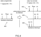
- FIG 4 illustrates possible drifts in the values of the two resistors R1 and R2 of a 2T2R memory cell.
- resistors R1 and R2 which have been programmed must each be checked in 1T1R mode with respect to a reference value (R REF ).
- the 1T1R reading of the first cell must return that the value read is less than the reference value "R1 ⁇ R REF ", and the 1T1R reading of the second cell must return that the value read is greater than the reference value “R2 > R REF ”, as illustrated by reference 400.
- resistors R1 and R2 may drift such that the condition “R2 > R1” is no longer valid. It can then, for a differential read operation in the 2T2R memory, be detected a logical '0' which is incorrect, instead of the logical '1' initially programmed.
- the right part of the figure 4 shows three possible scenarios under which the condition R2 > R1 becomes invalid.
- resistors R1 and R2 have drifted such that "R2 ⁇ R1" with “R1 > R REF " and "R2 ⁇ R REF ", i.e. both resistors are set either side of the reference value.
- resistors R1 and R2 have drifted such that "R2 ⁇ R1" but with “R1 > R REF " and “R2 > R REF ", i.e. both resistors are greater than the reference value.
- resistors R1 and R2 have drifted such that “R2 ⁇ R1" but with “R1 ⁇ R REF " and “R2 ⁇ R REF ", i.e. both resistors are smaller than the reference value.
- the cases of drift illustrated by the second and the third scenarios will be identified to improve error correction. Indeed, by identifying that the values of the two resistors R1 and R2 of the same 2T2R cell are "positioned" on the same side as the reference value, indicates that at least one of these resistors R1 or R2 has been subjected to a significant drift, or even the two resistors may have drifted), and therefore this may induce an erroneous 2T2R read operation.
- the general principle of the invention consists in identifying bits for which one or both resistor values have drifted in such a way that the two values are either greater than or less than a reference value. Such situations do not necessarily indicate that the bits which have been programmed will be detected in error during a reading in differential mode, but their identification indicates that they are likely to be in error. These bits are considered low bits and are referred to as "erasures".
- the identification of the erasures is made by the method of the invention by carrying out, in one embodiment, at least one reading in 1T1R mode on one of the two 1T1R cells of a 2T2R elementary cell. Reading 1T1R makes it possible to compare with a reference value, the value of one of the two resistive elements of the elementary cell which is addressed, and to determine whether the value read has drifted with respect to the reference value.
- FIG. 5 illustrates the steps of the error correction method of the invention in one embodiment.
- the method 500 operated for a 2T2R memory protected by an ECC, makes it possible to improve error correction by identifying erasures.
- the first stages of the process are identical to those of a conventional process, as described with reference to figure 2 , namely a step 502 of accessing an address of the 2T2R memory storing a code word, a step 504 of reading the code word stored at the read address, and a step 506 of setting implementation of an error correction and detection mechanism by an ECC coupled to the memory.
- the method makes it possible to check whether the ECC decoder indicates the presence of errors which affect a number of bits greater than a predefined threshold.
- the threshold value is set such that the number of bits affected by an error does not exceed the maximum number of erroneous bits that are correctable by the ECC decoder that is used, which is equivalent to determining that said number of affected bits is equal to the maximum number of erroneous bits that the ECC decoder can detect in a code word.
- step 520 the method ends in a conventional manner with step 520 with the supply of a code word corrected only by the ECC used in a conventional manner.
- the method continues with a mechanism for identifying erasures and correcting erroneous bits.
- the method comprises, before the decoding step 506, a step consisting in storing the value of each bit of the code word read in 2T2R mode in a register coupled to the resistive memory.
- the method makes it possible to perform at least one 1T1R reading (step 510 or 512) in each addressed elementary 2T2R cell, which consists in comparing the value of one of the two resistive elements of the addressed elementary 2T2R cells with a reference value 'R ERASURE ', in order to determine the value read.
- a 1T1R read is performed at the address indicated by the read command, on the resistive elements of each 2T2R elementary cell encoding the inverted values of the bits.
- a 1T1R read is performed at the address indicated by the read command, on the resistive elements of each 2T2R elementary cell encoding the non-inverted values of the bits.
- the method continues with a step 514 of comparing the bits read in 1T1R read (step 510 or 512) with the bits read in 2T2R read (step 504).
- step 514 of identification of erasures the method continues with a step 516 which consists in inverting in the corrected code word the said bits identified as likely to be erroneous, then a step 518 of correction and detection of errors by the ECC, in order to generate 520 a new corrected code word.
- the method allows a reading in 1T1R mode of the other resistor used for encoding in 2T2R mode.
- the step of performing at least one 1T1R reading may consist of performing a first 1T1R reading (step 510) of each first resistive element of the elementary cells addressed, in order to determine a first value read and performing a second reading 1T1R (step 512) of each second resistive element of the elementary cells addressed, in order to determine a second value read.
- the two electrical resistances of a 2T2R cell are considered to have been programmed so that one is smaller and the other larger than a reference value R REF (used during a previous operation of memory write). Consequently, by comparing, during the two read operations in 1T1R mode, each electrical resistance value with the same reference value R ERASURE , opposite logic values must be read in each 2T2R cell addressed during the read steps 510 and 512 .
- the comparison step to identify bits likely to be erroneous consists in comparing the first value read in 1T1R mode with the second value read in 1T1R mode.
- the identification of the bits liable to be erroneous consists in determining the bits for which the first value read in 1T1R read and the second value read in 1T1R read are identical. Indeed, in the case where for a 2T2R cell, the two values read in 1T1R reading are identical, it can be considered that at least one of the two electrical resistors has been subject to a significant drift since its programming in a low resistance state or a high resistance state. Consequently, the bit read in 2T2R mode from these two resistors could have been evaluated erroneously and it can then be considered as an erasure.
- the method continues with the steps 516 of bit inversion in the code word read in 2T2R, of decoding 518 by the ECC and of obtaining 520 of a corrected code.
- the data bits of the new corrected code word can be made available to the electronic system 310 which initiated the read command.
- the memory controller may signal a read error to the electronics.
- the R ERASURE reference value used during the read operation(s) in 1T1R mode is identical to the R REF reference value used during a programming operation in a 2T2R memory (which is done to ensure that the electrical heaters are programmed to LRS or HRS).
- FIG. 6 illustrates an example of a code word corrected by the method of the invention.
- a word 602 of a DEC-TED code (allowing the correction of single and double errors and the detection of triple errors) is read with three erroneous bits.
- the code word (1, 1, 1, 0, ..., 1, 0, 1, 0) indicates that the first '1', third '1' and fourth '0' bit are wrong.
- the DEC-TED decoder makes it possible to detect the presence of the three erroneous bits but not their position.
- the number of errors '3' is in this example greater than the threshold equal to '2' allowed by the DEC-TED in order to be able to correct them.
- the steps (510, 512, 514) of the method of the invention make it possible to identify erasures in the code word 602, i.e. the first bit '1', the fourth bit '0' and the nth bit '1'.
- Step 516 of the method of the invention makes it possible to invert the erasures bits, and the code word 604 becomes (0, 1, 1, 1, ..., 0, 0, 1, 0).
- Steps 518 and 520 of the method of the invention make it possible to correct the code word 604 and to obtain a new corrected code word 606 (0, 1, 0, 1, ..., 1, 0, 1, 0) which in this example no longer contains any erroneous bits.
- the inventors have found that for code words with 32 bits of data, the use of an ECC of the SEC-DED type instead of a DEC, and the use of an ECC of the DEC-TED type instead of a TEC, makes it possible to reduce the number of verification bits per code word by 42% and 28% respectively.
- FIG. 7 illustrates an embodiment of a circuit 700 making it possible to perform an inversion of bits read in 2T2R mode and identified as erasures through the comparison of the two values read in 1T1R mode.
- the circuit 700 can be used to replace each flip-flop of an output register of the 2T2R memory, for example the output register 340 of the picture 3 .
- the bit inversion circuit mainly comprises three synchronous flip-flops (702, 704, 706).
- a first flip-flop 702 can receive on its input in(2T2R) a bit read in 2T2R mode in the memory corresponding to step 504
- a second flip-flop 704 can receive on its input in(1T1R) one of the bits read in 1T1R corresponding to step 510
- a third flip-flop 706 can receive on its input in(1T1R) the other bit read in 1T1R mode corresponding to step 512.
- the flip-flops are clocked by a ⁇ clk' clock signal, and be initialized by 'set' and 'reset' signals (respectively 'rst 1 ' for the first flip-flop 702, 'rst 2 ' for the second flip-flop 704, and ⁇ set' for the third flip-flop 706).
- Each flip-flop is controlled by a signal 'in' generated by a memory controller, respectively 'in 1 ' for the first flip-flop 702, 'in 2 ' for the second flip-flop 704, 'in 3 ' for the third flip-flop 706.
- the Q 1 output of the first flip-flop 702 is coupled on the one hand to a first input of a multiplexer 712, and on the other hand to the input of an inverter 710 which is used to provide an inverted version of the stored bit in the first flip-flop 702.
- the output Q1 of inverter 710 becomes the second input of multiplexer 712.
- the outputs Q 2 and Q 3 of the second and third flip-flops 704 and 706 become the inputs of an XNOR logic gate 708.
- the output of the XNOR logic gate 708 becomes a 'salt' selection signal for the multiplexer 712.
- the value in output of the XNOR logic gate 708 is a logic '1' only when its two inputs are identical, i.e. corresponding to the bits respectively stored in the second and third flip-flops 704 and 706.
- the multiplexer 712 makes it possible to select and deliver an 'out' signal corresponding to the inverted value or to the non-inverted value of the bit stored in the first flip-flop 702, according to the logic value supplied by the XNOR gate 708, and therefore to the value of the 'sel' selection signal.
- the second latch 704 and the third latch 706 are initialized to different values at the start of each 2T2R memory access.
- the flip-flops 702, 704 and 706 can be replaced by latches.
- a high or low value is considered to represent a logical '1' or '0' respectively.
- the first flip-flop 702 and the second flip-flop 704 can be initialized to 0 if the signal 'rst 1 ', respectively 'rst 2 ', presents the value 0 during the rising edge of the clock signal 'clk'.
- the third flip-flop 706 can be initialized to 1 if the ⁇ set' signal is equal to 1 during the rising edge of the ⁇ clk' clock signal.
- each of these three flip-flops can change its state according to the input signal 'in' only if its control signal 'in' is equal to '1' during the rising edge of the clock signal ⁇ clk '.
- a first phase 'phase 1' reflects the reading of the first flip-flop (the signal 'in 1 ' equal to '1' during the rising edge of the signal ⁇ clk'), whose output Q 1 becomes logical '1'.
- phases 2 and 3 ie corresponding to the implementation of steps 510 to 514.
- the 'ecc_fail' signal changes to '1' to reflect that the result of step 508 indicates that errors remain which affect a number of bits greater than the predefined threshold.
- reading in 1T1R mode (the signal 'in 2 ' equal to '1' during the rising edge of the signal 'clk') provides the value of the output Q 2 of the second flip-flop 704, which is a ' logical 0'.
- reading in 1T1R mode (the signal 'at 3 ' equal to '1' during the rising edge of the signal 'clk') provides the value of the Q output 3 of the third flip-flop 706, which is a ' logical 0'.
- bit read in differential mode is equal to '1' and the two bits read in 1T1R mode are equal to '0', which indicates that the bit read in differential mode can be identified as erasure.
- the last line of the timing diagram reflects the value of the 'out' output signal which toggles to invert the value of the bit identified as erasure.
- FIG 9 illustrates another embodiment of a circuit 900 making it possible to perform an inversion of bits identified as erasures according to the method of the invention.
- the elements in common with the circuit presented in figure 7 keep the same references and are not described again.
- this erasure bit inversion device 900 replaces each conventional flip-flop in the output register 340 of the resistive memory.
- the circuit comprises a second XNOR logic gate 902 and a second multiplexer 904 in addition.
- the second XNOR logic gate 902 takes as input the output of the first flip-flop 702, and the output of the second flip-flop 704 to compare them.
- the second multiplexer 904 takes as input the output of the first XNOR gate 708 and the output of the second XNOR gate 902, to supply a select signal 'sel' to the first multiplexer 712, when it is activated by a control signal 'in'.
- the first value read in 1T1R mode is stored in the second flip-flop 704 and that this value is compared with the value read in 2T2R mode which is stored in the first flip-flop 702.
- the logic gate that makes the comparison must be an XNOR type gate, as in the example of the figure 9 .
- the logic gate that makes the comparison must be an XOR type gate (not shown).
- the second multiplexer 904 is driven by an 'en' signal generated by the memory controller.
- provision may be made to have the signal 'en' equal to a logical '1' only during the cycle in which the values of the first 702 and of the second flip-flop 704 are compared.
- each functional module for encoding, counting, comparison and inversion can be implemented by a dedicated module such as an ASIC.
- the invention can be implemented from hardware and/or software elements. It may be available as a computer program product executed by a dedicated processor or by a memory controller of a storage system, and which includes code instructions for executing the steps of the methods in their various embodiments.
Abstract
L'invention concerne une solution pour améliorer la correction d'erreurs dans une mémoire résistive 2T2R protégée par un code correcteur d'erreur. De manière générale, le principe de l'invention repose sur un procédé qui permet par des lectures 1T1R d'identifier dans un mot de code stocké en mémoire, des bits susceptibles d'être erronés dits « erasures », puis d'inverser ces bits dans le mot de code stocké afin de générer un nouveau mot corrigé par l'ECC.The invention relates to a solution for improving error correction in a 2T2R resistive memory protected by an error-correcting code. In general, the principle of the invention is based on a process which makes it possible, by means of 1T1R readings, to identify in a code word stored in memory, bits likely to be erroneous, called "erasures", then to invert these bits. in the stored codeword to generate a new ECC-corrected word.
Description
L'invention se situe dans le domaine des mémoires résistives ou RRAM pour « Résistive Random Access Memory » selon la terminologie anglo-saxonne, et concerne plus particulièrement un procédé et un dispositif permettant d'améliorer la correction d'erreurs dans des mémoires résistives de type 2T2R.The invention lies in the field of resistive memories or RRAM for "Resistive Random Access Memory" according to the English terminology, and relates more particularly to a method and a device making it possible to improve error correction in resistive memories of type 2T2R.
Les mémoires résistives sont des mémoires non-volatiles présentant une vitesse de fonctionnement élevée, une faible consommation d'énergie électrique et une grande durée de vie. Pour ces raisons, les mémoires résistives sont des candidates prometteuses pour remplacer à la fois les mémoires vives et les mémoires non-volatiles actuelles telles que les mémoires de type flash.Resistive memories are non-volatile memories with high operating speed, low power consumption and long life. For these reasons, resistive memories are promising candidates for replacing both random access memories and current non-volatile memories such as flash-type memories.
Il existe plusieurs technologies de mémoires résistives. On peut notamment citer les mémoires résistives à pont conducteur, également appelées CBRAM (pour « Conductive-Bridging Random-Access Memory » selon la terminologie anglo-saxonne), ou les mémoires résistives à base d'oxyde, également appelées OxRAM (pour « Oxide-based Random-Access Memory » selon la terminologie anglo-saxonne), ou encore les mémoires à changement de phase, également appelées PCM (pour « Phase Change Memory » selon la terminologie anglo-saxonne).There are several resistive memory technologies. Mention may in particular be made of resistive memories with a conductive bridge, also called CBRAM (for “Conductive-Bridging Random-Access Memory” according to the English terminology), or resistive memories based on oxide, also called OxRAM (for “Oxide -based Random-Access Memory” according to the Anglo-Saxon terminology), or phase change memories, also called PCM (for “Phase Change Memory” according to the Anglo-Saxon terminology).
Une mémoire résistive est composée d'une multitude de cellules mémoires résistives agencées en lignes et colonnes de manière à former une matrice. Une cellule mémoire RRAM est dotée d'au moins un élément résistif dont on peut modifier la conductance.A resistive memory is made up of a multitude of resistive memory cells arranged in rows and columns so as to form a matrix. An RRAM memory cell has at least one resistive element whose conductance can be modified.
Typiquement, une cellule mémoire RRAM dans son état initial a une structure métallique isolante et est dans un état de haute résistance (HRS) (pour « High Résistance State » selon la terminologie anglo-saxonne). Avant leur utilisation, certains types de mémoire résistive, telles que les mémoires OxRAM ou CBRAM, nécessitent une activation électrique. L'application d'une impulsion haute tension externe à travers la cellule RRAM permet la formation de chemins conducteurs dans la couche de commutation et la cellule RRAM est commutée dans un état à faible résistance (LRS) (pour « Low Resistance State » selon la terminologie anglo-saxonne). Le processus général de cette rupture de la structure métallique isolante de la cellule est généralement appelé «électroformage» (ou « forming » selon la terminologie anglo-saxonne).Typically, an RRAM memory cell in its initial state has an insulating metallic structure and is in a high resistance state (HRS) (for “High Resistance State” according to the English terminology). Prior to use, some types of resistive memory, such as OxRAM or CBRAM, require electrical activation. Application of an external high voltage pulse across the RRAM cell allows conductive paths to be formed in the switching layer and the RRAM cell is switched into a low resistance state (LRS) (for “Low Resistance State” according to English terminology). The general process of this breaking of the insulating metallic structure of the cell is generally called “electroforming” (or “forming” according to the English terminology).
Le matériau diélectrique qui est disposé entre les deux électrodes conductrices de la cellule va permettre à la cellule de basculer de manière réversible entre deux états de résistance HRS et LRS, chacun des états permettant de stocker un bit d'information dans la cellule mémoire.The dielectric material which is arranged between the two conductive electrodes of the cell will allow the cell to reversibly switch between two resistance states HRS and LRS, each of the states making it possible to store a bit of information in the memory cell.
Pour programmer une cellule mémoire, une tension de programmation est appliquée entre les électrodes de la cellule mémoire. Il peut s'agir d'une tension d'écriture pour écrire la cellule mémoire, c'est-à-dire la placer dans l'état LRS, ou d'une tension d'effacement pour effacer la cellule mémoire, c'est-à-dire la placer dans l'état HRS. Cependant, après une opération de programmation, il peut arriver que la cellule mémoire ne passe pas dans l'état de résistance souhaité. Pour cette raison, il est généralement effectué une vérification que la cellule mémoire est correctement programmée en comparant sa valeur de résistance R à une valeur seuil de résistance prédéfinie RREF.To program a memory cell, a programming voltage is applied between the electrodes of the memory cell. It can be a write voltage to write the memory cell, i.e. put it in the LRS state, or an erase voltage to erase the memory cell, i.e. ie place it in the HRS state. However, after a programming operation, it may happen that the memory cell does not go into the desired resistance state. For this reason, a verification is generally carried out that the memory cell is correctly programmed by comparing its resistance value R with a predefined resistance threshold value R REF .
La
Cependant, l'écart entre la plus faible valeur correspondant à un niveau HRS et la plus haute valeur correspondant au niveau LRS, également appelé « fenêtre mémoire », est souvent faible. Dès lors, on utilise couramment un « encodage différentiel » ou encodage 2T2R pour coder une valeur binaire à mémoriser. Un bit d'information peut alors être encodé dans une cellule mémoire dite 2T2R telle qu'illustrée de manière simplifiée sur la
Comme chacun des états HRS et LRS peut être associé à une valeur logique, i.e. 1 ou 0, on peut considérer que dans une cellule 2T2R un des deux éléments résistifs encode le bit à programmer en version non-inversée tandis que l'autre élément résistif encode le même bit en version inversée. Par exemple, un '1' logique est encodé en programmant le résistor de la première cellule 1T1R dans un état HRS et le résistor de la deuxième cellule 1T1R dans un état LRS, et un '0' logique est encodé en programmant le résistor de la première cellule 1T1R dans un état LRS et le résistor de la deuxième cellule dans un état HRS.As each of the HRS and LRS states can be associated with a logic value, i.e. 1 or 0, one can consider that in a 2T2R cell one of the two resistive elements encodes the bit to be programmed in a non-inverted version while the other resistive element encodes the same bit in inverted version. For example, a logical '1' is encoded by programming the resistor of the first 1T1R cell in an HRS state and the resistor of the second 1T1R cell in an LRS state, and a logical '0' is encoded by programming the resistor of the first cell 1T1R in an LRS state and the resistor of the second cell in an HRS state.
Ainsi, en encodage différentiel, chaque bit d'information est encodé dans une cellule élémentaire 2T2R formée de deux éléments résistifs écrits en opposition d'état, c'est-à-dire un des éléments résistifs avec un niveau HRS et l'autre un niveau LRS. Les niveaux respectifs de résistance des deux éléments résistifs sont déterminés toujours dans le même ordre entre les deux éléments, et définissent alors si l'on est en présence d'un '0' ou d'un '1' logique, suivant que cela correspond à l'état HRS-LRS ou à l'état LRS-HRS.Thus, in differential encoding, each bit of information is encoded in a 2T2R elementary cell formed of two resistive elements written in opposition of state, i.e. one of the resistive elements with an HRS level and the other a LRS level. The respective levels of resistance of the two resistive elements are always determined in the same order between the two elements, and then define whether we are in the presence of a '0' or a logical '1', depending on whether it corresponds in the HRS-LRS state or in the LRS-HRS state.
Lors d'une opération d'écriture dans une cellule mémoire 1T1R ou une cellule mémoire 2T2R, il faut s'assurer que chaque résistance électrique qui doit être programmée à l'état HRS ou l'état LRS est respectivement soit plus grande, soit plus petite qu'une valeur de référence RREF. La comparaison d'une résistance électrique avec la valeur RREF est faite par une opération de lecture au cours de laquelle la résistance programmée est comparée à la valeur RREF à l'aide d'un amplificateur de détection ou SA (pour « Sense Amplifier» selon la terminologie anglo-saxonne) illustré par le composant 104 sur la
Sur la
Sur la
Toutes les opérations de lecture dans les mémoires 1T1R sont effectuées en mode 1T1R. Pour lire efficacement les données de la cellule RRAM, une petite tension de lecture qui ne perturbe pas l'état courant de la cellule est appliquée pour déterminer dans quel état logique est la cellule.All read operations in 1T1R memories are performed in 1T1R mode. To efficiently read data from the RRAM cell, a small read voltage that does not disturb the current state of the cell is applied to determine what logic state the cell is in.
Dans les mémoires où l'information est encodée en mode 2T2R, les opérations de lecture, hors celle de vérification de la programmation, peuvent être effectuées en mode 2T2R aussi appelé lecture en mode différentiel ou lecture 2T2R. Les valeurs des deux résistances présentes dans chaque cellule mémoire 2T2R qui est adressée, sont comparées entre elles à l'aide d'un amplificateur de détection SA.In the memories where the information is encoded in 2T2R mode, the read operations, apart from that of verification of the programming, can be carried out in 2T2R mode also called reading in differential mode or 2T2R reading. The values of the two resistors present in each 2T2R memory cell which is addressed are compared with each other using a sense amplifier SA.
L'usage d'une mémoire implique de fréquentes transitions entre un état HRS et un état LRS et réciproquement, et chaque événement de commutation entre ces états résistifs peut introduire des dommages, les valeurs des résistances programmées pouvant changer à cause de phénomènes de relaxation, et entraîner alors une dégradation des performances de la RRAM.The use of a memory involves frequent transitions between an HRS state and an LRS state and vice versa, and each switching event between these resistive states can introduce damage, the values of the programmed resistances being able to change due to relaxation phenomena, and then lead to a degradation of the performance of the RRAM.
Le temps de rétention de l'information dans une mémoire résistive dépend alors (a) des opérations de lecture, (b) des températures d'utilisation et/ou (c) des champs magnétiques élevés dans le cas des mémoires magnétiques.The information retention time in a resistive memory then depends on (a) read operations, (b) operating temperatures and/or (c) high magnetic fields in the case of magnetic memories.
De plus, les tensions de commutation sont aussi des paramètres présentant un degré élevé de variation. Les variations de la commutation de résistance comprennent des fluctuations temporelles (cycle à cycle) et des fluctuations spatiales (appareil à appareil).In addition, switching voltages are also parameters with a high degree of variation. Variations in resistance switching include temporal fluctuations (cycle to cycle) and spatial fluctuations (device to device).
Par ailleurs, les mémoires résistives présentent également une non-uniformité cellule à cellule qui dégrade également les performances de la mémoire en réduisant la marge de mémoire entre deux états. L'origine de cette variabilité est attribuée aux non-uniformités du processus de fabrication telles que l'épaisseur du film de commutation, les dommages de gravure et la rugosité de surface des électrodes.Furthermore, resistive memories also exhibit cell-to-cell non-uniformity which also degrades memory performance by reducing the memory margin between two states. The origin of this variability is attributed to manufacturing process non-uniformities such as switch film thickness, etch damage, and electrode surface roughness.
Ces variations entrainent que les résistances des mémoires résistive qui sont programmées dans l'état LRS peuvent dériver vers un état HRS, et les résistances qui sont programmées dans l'état HRS peuvent dériver vers un état LRS. Dès lors, ce glissement des valeurs des résistances programmées peut engendrer des erreurs lors des opérations de lecture, et diminuer la performance des mémoires.These variations cause the resistances of the resistive memories which are programmed in the LRS state to drift towards an HRS state, and the resistances which are programmed to the HRS state may drift towards an LRS state. Consequently, this sliding of the values of the programmed resistors can generate errors during the read operations, and reduce the performance of the memories.
Une manière courante d'améliorer la performance des mémoires RRAM est de diminuer leur taux d'erreur. Pour réduire le taux d'erreur des mémoires, une solution couramment utilisée consiste à utiliser un code correcteur d'erreurs ou ECC (pour « Error Correcting Code » selon la terminologie anglo-saxonne) qui encode les données avant leur écriture en mémoire. Lors de l'encodage de données avec un code ECC, des bits de vérification sont ajoutés aux bits de données, les bits de vérification représentant une information redondante calculée à partir des bits de données, qui permet la détection et la correction des erreurs affectant aussi bien les bits de données que les bits de vérification. L'ensemble des bits de données et des bits de vérification forme un mot de code.A common way to improve the performance of RRAM memories is to reduce their error rate. To reduce the error rate of memories, a commonly used solution consists in using an error correcting code or ECC (for "Error Correcting Code" according to the English terminology) which encodes the data before they are written in memory. When encoding data with an ECC code, check bits are added to the data bits, the check bits representing redundant information calculated from the data bits, which allows the detection and correction of errors also affecting both data bits and check bits. The set of data bits and check bits forms a code word.
La demande de brevet
En présence d'un taux d'erreurs élevé, une solution est d'utiliser des ECCs de plus en plus puissants. Cependant, cela entraine un surcoût en termes de surface de stockage pour les bits de vérification et de surface, de latence et de consommation du décodeur ECC.In the presence of a high error rate, one solution is to use more and more powerful ECCs. However, this entails an additional cost in terms of storage surface for the verification bits and surface, latency and consumption of the ECC decoder.
Une approche pour éviter l'utilisation d'un ECC puissant, est de réduire le taux d'erreurs primaire, c'est-à-dire le taux d'erreurs en sortie du circuit mémoire qui serait obtenu sans l'utilisation d'un ECC. Pour réduire le taux d'erreurs primaire, une méthode consiste à utiliser des mémoires 2T2R au lieu de mémoires 1T1R. Cependant, il reste des cas où même avec l'utilisation d'une mémoire 2T2R le taux d'erreurs primaire reste élevé.One approach to avoid the use of a powerful ECC, is to reduce the primary error rate, that is to say the error rate at the output of the memory circuit which would be obtained without the use of a ECC. To reduce the primary error rate, one method is to use 2T2R memories instead of 1T1R memories. However, there are still cases where even with the use of a 2T2R memory the primary error rate remains high.
Aussi, dans ces situations ou encore celles où il faudrait choisir un ECC avec un moindre surcoût et donc une capacité de correction plus faible, une solution connue est d'identifier les cellules qui sont dans un état pouvant être considéré comme faible, c'est-à-dire des cellules susceptibles de délivrer un bit erroné, ces bits étant désignés comme « erasure », puis d'utiliser cette information pour améliorer la correction d'erreurs.Also, in these situations or those where it would be necessary to choose an ECC with a lower additional cost and therefore a lower correction capacity, a solution known is to identify the cells which are in a state that can be considered weak, that is to say cells likely to deliver an erroneous bit, these bits being designated as "erasure", then to use this information to improve error correction.
L'article de
L'article de
Aussi, face à la problématique générale de la dérive des valeurs de résistance dans les cellules mémoires résistives RRAM, et face aux limites des solutions connues basées sur l'utilisation de code correcteur d'erreur, il existe le besoin d'une solution pour diminuer les erreurs de lecture dans les mémoires résistives RRAM, en particulier dans les mémoires RRAM 2T2R.Also, faced with the general problem of the drift of resistance values in RRAM resistive memory cells, and faced with the limits of known solutions based on the use of error-correcting code, there is a need for a solution to reduce read errors in resistive RRAM memories, in particular in 2T2R RRAM memories.
La présente invention répond à ce besoin.The present invention meets this need.
L'invention a pour objet une solution pour améliorer la correction d'erreurs dans les mémoires résistives protégées par un code correction d'erreurs.The subject of the invention is a solution for improving error correction in resistive memories protected by an error correction code.
De manière générale, le principe de l'invention repose sur un procédé qui permet d'identifier dans un mot de code programmé dans une mémoire résistive 2T2R protégée par un code correcteur d'erreur, des bits susceptibles d'être erronés, appelés bit(s) faible(s) ou « erasure(s) », puis d'inverser ces bits afin de générer un nouveau mot qui peut être corrigé par le décodeur du code correcteur d'erreur.In general, the principle of the invention is based on a method which makes it possible to identify, in a code word programmed in a 2T2R resistive memory protected by an error-correcting code, bits likely to be erroneous, called bit( s) weak(s) or “erasure(s)”, then inverting these bits in order to generate a new word which can be corrected by the decoder of the error correcting code.
Avantageusement, le procédé de la présente invention ne nécessite pas de modification de la matrice mémoire. La méthode proposée n'a pas d'impact sur les opérations d'écriture dans les mémoires résistives concernées.Advantageously, the method of the present invention does not require modification of the memory matrix. The proposed method has no impact on the write operations in the resistive memories concerned.
Ainsi l'objet de l'invention est de pallier les inconvénients des solutions connues par une solution qui ne nécessite pas d'opérations impliquant l'utilisation de valeurs de référence supplémentaires.Thus the object of the invention is to overcome the drawbacks of the known solutions by a solution which does not require operations involving the use of additional reference values.
Pour parvenir au but recherché, il est proposé un procédé de correction d'erreurs d'un mot de code stocké dans une mémoire résistive de type 2T2R, un mot de code étant composé de bits de données et de bits de vérification, la mémoire résistive 2T2R comprenant une matrice de cellules mémoires résistives 2T2R élémentaires où chaque cellule élémentaire comprend deux transistors et deux éléments résistifs pour stocker la valeur non-inversée et la valeur inversée d'un bit, et pour lire les bits stockés en mode différentiel, la lecture en mode différentiel ou lecture 2T2R consistant à comparer l'une par rapport à l'autre, les valeurs du premier et deuxième élément résistif de la cellule élémentaire utilisée pour stocker chaque bit d'un mot à une adresse indiquée, afin de déterminer la valeur lue. Le procédé comprend au moins les étapes consistant à :
- déterminer, après une opération de correction d'erreurs par un code correcteur d'erreur couplé à la mémoire résistive, qu'un mot de code lu en lecture 2T2R contient des erreurs non corrigées qui affectent un nombre de bits supérieur à un seuil prédéfini ;
- effectuer au moins une lecture en mode simple ou lecture 1T1R du mot de code stocké, consistant à comparer à une valeur de référence RERASURE, la valeur d'un des deux éléments résistifs des cellules élémentaires adressées pour chaque bit du mot de code, afin de déterminer la valeur lue ;
- comparer pour chaque bit du mot de code, la valeur lue par la dite au moins une lecture 1T1R à la valeur lue en lecture 2T2R pour identifier des bits susceptibles d'être erronés, lesdits bits susceptibles d'être erronés étant :
- des bits pour lesquels la valeur lue en lecture 1T1R est identique à la valeur lue en lecture 2T2R, si ladite au moins une lecture 1T1R se fait sur les éléments résistifs de la cellule élémentaire encodant les valeurs inversées des bits ; ou
- des bits pour lesquels la valeur lue en lecture 1T1R est différente de la valeur lue en lecture 2T2R, si ladite au moins une lecture 1T1R se fait sur les éléments résistifs de la cellule élémentaire encodant les valeurs non-inversées des bits ;
- inverser, dans ledit mot de code lu en lecture 2T2R, lesdits bits identifiés comme susceptibles d'être erronés ; et
- corriger avec le code correcteur d'erreur ledit mot de code obtenu après l'étape d'inversion.
- determining, after an error correction operation by an error correcting code coupled to the resistive memory, that a code word read in 2T2R read mode contains uncorrected errors which affect a number of bits greater than a predefined threshold;
- perform at least one reading in simple mode or 1T1R reading of the stored code word, consisting in comparing with a reference value R ERASURE , the value of one of the two resistive elements of the elementary cells addressed for each bit of the code word, in order to determine the value read;
- compare for each bit of the code word, the value read by said at least one 1T1R reading with the value read in 2T2R reading to identify bits likely to be erroneous, said bits likely to be erroneous being:
- bits for which the value read in 1T1R reading is identical to the value read in 2T2R reading, if said at least one 1T1R reading is done on the resistive elements of the elementary cell encoding the inverted values of the bits; Or
- bits for which the value read in 1T1R reading is different from the value read in 2T2R reading, if said at least one 1T1R reading is done on the resistive elements of the elementary cell encoding the non-inverted values of the bits;
- inverting, in said code word read in 2T2R reading, said bits identified as likely to be erroneous; And
- correcting said code word obtained after the inversion step with the error correction code.
Selon des modes de réalisation alternatifs ou combinés :
- L'étape de déterminer qu'un mot de code contient des erreurs non corrigées qui affecte un nombre de bits supérieur à un seuil prédéfini, consiste à déterminer que ledit nombre de bits affectés est égal au nombre maximum de bits erronés que le décodeur du code correcteur d'erreur peut détecter dans un mot de code.
- Les étapes de lecture 1T1R et de comparaison de valeur lue consistent à : effectuer une première lecture 1T1R de chaque premier élément résistif des cellules élémentaires adressées pour chaque bit du mot de code, afin de déterminer une première valeur lue ; effectuer une deuxième lecture 1T1R de chaque deuxième élément résistif des cellules élémentaires adressées pour chaque bit du mot de code, afin de déterminer une deuxième valeur lue ; et comparer la première valeur lue en mode 1T1R à la deuxième valeur lue en mode 1T1R, pour identifier des bits susceptibles d'être erronés comme étant des bits pour lesquels la première valeur lue et la deuxième valeur lue sont identiques.
- Le procédé comprend avant l'étape de décodage, une étape consistant à stocker la valeur de chaque bit du mot de code lu en mode 2T2R dans un registre couplé à la mémoire résistive.
- L'étape de corriger le mot de code obtenu après inversion, comprend des étapes consistant à :
- stocker la valeur de chaque bit dudit mot de code obtenu après inversion dans un registre couplé à la mémoire résistive ;
- corriger par le code correcteur d'erreur ledit mot de code stocké ; et
- stocker le mot de code corrigé dans le registre de sortie du décodeur du code correcteur d'erreur.
- L'étape de comparaison comprend des étapes consistant à :
- stocker la valeur de chaque bit lu en mode 1T1R dans un registre couplé à la mémoire résistive ; et
- comparer la valeur de chaque bit stocké à la valeur de chaque bit du mot de code lu en mode 2T2R.
- L'étape d'effectuer au moins une lecture en mode 1T1R consiste à comparer la valeur lue à une valeur de référence RERASURE qui peut être identique à la valeur de référence utilisée pour programmer les cellules élémentaires de la mémoire résistive.
- The step of determining that a code word contains uncorrected errors which affects a number of bits greater than a predefined threshold, consists in determining that said number of affected bits is equal to the maximum number of erroneous bits that the decoder of the code error checker can detect in a code word.
- The 1T1R read and read value comparison steps consist of: performing a first 1T1R read of each first resistive element of the elementary cells addressed for each bit of the code word, in order to determine a first read value; carry out a second reading 1T1R of each second resistive element of the elementary cells addressed for each bit of the code word, in order to determine a second value read; and comparing the first value read in 1T1R mode with the second value read in 1T1R mode, to identify bits likely to be erroneous as being bits for which the first value read and the second value read are identical.
- The method comprises, before the decoding step, a step consisting in storing the value of each bit of the code word read in 2T2R mode in a register coupled to the resistive memory.
- The step of correcting the code word obtained after inversion includes steps consisting of:
- storing the value of each bit of said code word obtained after inversion in a register coupled to the resistive memory;
- correcting said stored code word by the error correcting code; And
- storing the corrected code word in the output register of the error correcting code decoder.
- The comparison step includes steps of:
- storing the value of each bit read in 1T1R mode in a register coupled to the resistive memory; And
- comparing the value of each bit stored with the value of each bit of the code word read in 2T2R mode.
- The step of performing at least one reading in 1T1R mode consists in comparing the value read with a reference value R ERASURE which may be identical to the reference value used to program the elementary cells of the resistive memory.
L'invention a aussi pour objet un programme d'ordinateur comportant des instructions de code pour l'exécution des étapes du procédé de correction d'erreurs, lorsque ledit programme est exécuté par un processeur.The invention also relates to a computer program comprising code instructions for the execution of the steps of the error correction method, when said program is executed by a processor.
L'invention couvre aussi un dispositif de correction d'erreurs comprenant des moyens permettant de mettre en oeuvre les étapes du procédé de correction d'erreurs d'un mot de code stocké dans une mémoire résistive de type 2T2R, tel que revendiqué.The invention also covers an error correction device comprising means making it possible to implement the steps of the method for correcting errors of a code word stored in a resistive memory of the 2T2R type, as claimed.
Dans un mode de réalisation, le code correcteur d'erreur est un circuit de type SEC-DED.In one embodiment, the error correcting code is an SEC-DED type circuit.
Dans une variante de réalisation, le code correcteur d'erreur est un circuit de type DEC-TED.In a variant embodiment, the error correcting code is a DEC-TED type circuit.
Un autre objet de l'invention couvre tout système électronique de type FPGA ou ASIC comprenant un dispositif de correction d'erreurs tel que revendiqué.Another object of the invention covers any electronic system of the FPGA or ASIC type comprising an error correction device as claimed.
D'autres caractéristiques, détails et avantages de l'invention ressortiront à la lecture de la description faite en référence aux dessins annexés donnés à titre d'exemple et qui représentent, respectivement :
- La
figure 1a et lafigure 1b illustrent respectivement des exemples d'implémentation d'une cellule mémoire 1T1R et d'une cellule mémoire 2T2R ; - La
figure 2 illustre les étapes d'un procédé conventionnel de lecture dans une mémoire 2T2R protégée par un ECC ; - La
figure 3 illustre un système général permettant de mettre en oeuvre les étapes d'un procédé de lecture conventionnelle dans une mémoire 2T2R protégée par un ECC ; - La
figure 4 illustre la dérive des valeurs des résistances d'une cellule mémoire résistive 2T2R ; - La
figure 5 illustre les étapes du procédé de correction d'erreurs de l'invention dans un mode de réalisation ; - La
figure 6 montre un exemple d'un mot de code corrigé par le procédé de l'invention ; - La
figure 7 illustre un mode de réalisation d'un circuit permettant de réaliser une inversion de bits identifiés comme erasures ; - La
figure 8 est un chronogramme de différents signaux opérant sur le circuit de lafigure 7 ; et - La
figure 9 illustre un autre mode de réalisation d'un circuit permettant de réaliser une inversion de bits identifiés comme erasures.
- There
picture 1a and thefigure 1b respectively illustrate examples of implementation of a 1T1R memory cell and a 2T2R memory cell; - There
figure 2 illustrates the steps of a conventional method of reading in a 2T2R memory protected by an ECC; - There
picture 3 - There
figure 4 illustrates the drift of the resistance values of a 2T2R resistive memory cell; - There
figure 5 illustrates the steps of the error correction method of the invention in one embodiment; - There
figure 6 shows an example of a code word corrected by the method of the invention; - There
figure 7 illustrates an embodiment of a circuit making it possible to perform an inversion of bits identified as erasures; - There
figure 8 is a timing diagram of various signals operating on the circuit of thefigure 7 ; And - There
figure 9 illustrates another embodiment of a circuit making it possible to perform an inversion of bits identified as erasures.
La
Après que le mot de code soit lu 204 en mode 2T2R à l'adresse indiquée par la commande de lecture, dans une étape suivante 206, le décodeur de l'ECC est utilisé de manière conventionnelle (i.e. le décodeur cherche la localisation d'erreurs mais n'utilise pas d'informations sur d'éventuelles erasures) pour détecter et corriger des bits erronés dans le mot de code lu.After the code word is read 204 in 2T2R mode at the address indicated by the read command, in a
Selon le type d'ECC et le nombre d'erreurs, tous les bits erronés peuvent ou non être corrigés, et suite à l'étape 206 de décodage ECC, un mot de code corrigé est disponible, et dont les bits des données peuvent être mis à la disposition du système électronique qui a lancé la commande de lecture.Depending on the type of ECC and the number of errors, all the erroneous bits may or may not be corrected, and following the
Sans limitation, un ECC connu est le circuit SEC-DED (acronyme de l'anglicisme « Single Error Correction-Double Error Détection ») qui permet la correction des erreurs sur un seul bit (SEC) et la détection des erreurs sur deux bits (DED). L'homme du métier pourra se reporter aux nombreux documents disponibles de la littérature qui décrivent différents types de circuits code correcteur d'erreurs et mécanismes de correction et détection d'erreurs par un ECC.Without limitation, a known ECC is the SEC-DED (acronym for "Single Error Correction-Double Error Detection") circuit which provides single-bit error correction (SEC) and double-bit error detection ( DED). Those skilled in the art may refer to the numerous documents available in the literature which describe different types of error-correcting code circuits and mechanisms for correcting and detecting errors by an ECC.
La
Les commandes de lecture mémoire sont initialisées depuis un système électronique hôte 310. Le système électronique 310 peut être un circuit à base de processeurs, de multiprocesseurs, de FPGA (acronyme de « Field-Programmable Gate Array » en anglais) ou d'ASIC (acronyme de « Application Spécifie Integrated Circuit » en anglais).The memory read commands are initialized from a host
Dans un mode de réalisation, le système électronique 310 peut être un contrôleur mémoire implémenté dans un système de stockage.In one embodiment,
Les bits du mode de code lu dans la mémoire 2T2R 350 sont stockés dans un registre de sortie 340 de la mémoire. La mémoire résistive 2T2R 350 peut être organisée comme une matrice de cellules mémoires résistives 2T2R élémentaires où chaque cellule élémentaire comprend deux transistors et deux éléments résistifs pour encoder la valeur non-inversée et la valeur inversée d'un bit, en programmant une des deux résistances en LRS et l'autre en HRS, et pour faire une lecture 2T2R des bits encodés.The bits of the code mode read from the
Les bits lus sont transférés de la mémoire vers un décodeur ECC 330 afin de corriger les éventuelles erreurs survenues lors de leur stockage et/ou de leur lecture. Suite à l'opération de décodage ECC, les bits de données du mot de code corrigé peuvent être stockés dans un registre de sortie 320 du décodeur ECC, et mis à disposition du système électronique 310.The bits read are transferred from the memory to an
Comme expliqué précédemment, les valeurs de résistance de chaque élément résistif d'une cellule élémentaire 2T2R peuvent dériver dans le temps. La
Pour expliquer ces dérives, on peut prendre pour hypothèse qu'un '1' logique est stocké dans une cellule 2T2R, en programmant la première résistance R1 à un état à faible résistance (LRS) et en programmant la deuxième résistance R2 à un état à haute résistance (HRS), tel que « R2 > R1 ».To explain these drifts, one can assume that a logical '1' is stored in a 2T2R cell, by programming the first resistor R1 to a low resistance (LRS) state and by programming the second resistor R2 to a low resistance state. high resistance (HRS), such as "R2 > R1".
Lors d'une opération d'écriture en mémoire, les résistances R1 et R2 qui ont été programmées doivent être vérifiées chacune en mode 1T1R par rapport à une valeur de référence (RREF).During a memory write operation, resistors R1 and R2 which have been programmed must each be checked in 1T1R mode with respect to a reference value (R REF ).
Selon la programmation indiquée, la lecture 1T1R de la première cellule doit retourner que la valeur lue est inférieure à la valeur de référence « R1 < RREF », et la lecture 1T1R de la deuxième cellule doit retourner que la valeur lue est supérieure à la valeur de référence « R2 > RREF », tel qu'illustré par la référence 400.According to the indicated programming, the 1T1R reading of the first cell must return that the value read is less than the reference value "R1 < R REF ", and the 1T1R reading of the second cell must return that the value read is greater than the reference value “R2 > R REF ”, as illustrated by
Avec l'augmentation du temps de stockage, les valeurs des résistances R1 et de R2 peuvent dériver de telle sorte que la condition « R2 > R1 « n'est plus valide. Il peut alors, pour une opération de lecture en différentiel dans la mémoire 2T2R, être détecté un '0' logique qui est incorrect, au lieu du '1' logique initialement programmé.With increasing storage time, the values of resistors R1 and R2 may drift such that the condition “R2 > R1” is no longer valid. It can then, for a differential read operation in the 2T2R memory, be detected a logical '0' which is incorrect, instead of the logical '1' initially programmed.
La partie de droite de la
Dans le deuxième scénario 404, les résistances R1 et R2 ont dérivé de telle sorte que « R2 < R1 » mais avec « R1 > RREF » et « R2 > RREF », c'est-à-dire que les deux résistances sont plus grandes que la valeur de référence.In the
Dans le troisième scénario 406, les résistances R1 et R2 ont dérivé de telle sorte que « R2 < R1 » mais avec « R1 < RREF » et « R2 < RREF », c'est-à-dire que les deux résistances sont plus petites que la valeur de référence.In the
Selon le procédé de l'invention, les cas de dérive illustrés par le deuxième et le troisième scénarios vont être identifiés pour améliorer la correction d'erreurs. En effet, en identifiant que les valeurs des deux résistances R1 et R2 d'une même cellule 2T2R sont « positionnées » du même côté que la valeur de référence, indique qu'au moins une de ces résistances R1 ou R2 a été soumises à une dérive significative, voire les deux résistances ont pu dériver), et dès lors cela peut induire une opération de lecture 2T2R erronée.According to the method of the invention, the cases of drift illustrated by the second and the third scenarios will be identified to improve error correction. Indeed, by identifying that the values of the two resistors R1 and R2 of the same 2T2R cell are "positioned" on the same side as the reference value, indicates that at least one of these resistors R1 or R2 has been subjected to a significant drift, or even the two resistors may have drifted), and therefore this may induce an erroneous 2T2R read operation.
Ainsi, le principe général de l'invention consiste à identifier des bits pour lesquels une ou les deux valeurs de résistances ont dérivé de telle sorte que les deux valeurs sont soit supérieures, soit inférieures à une valeur de référence. De telles situations n'indiquent pas nécessairement que les bits qui ont été programmés vont être détectés en erreur lors d'une lecture en mode différentiel, mais leur identification indique qu'ils sont susceptibles d'être erronés. Ces bits sont considérés comme étant des bits faibles et sont désignés comme étant des « erasures ».Thus, the general principle of the invention consists in identifying bits for which one or both resistor values have drifted in such a way that the two values are either greater than or less than a reference value. Such situations do not necessarily indicate that the bits which have been programmed will be detected in error during a reading in differential mode, but their identification indicates that they are likely to be in error. These bits are considered low bits and are referred to as "erasures".
L'identification des erasures, est faite par le procédé de l'invention en effectuant dans un mode de réalisation, au moins une lecture en mode 1T1R sur une des deux cellules 1T1R d'une cellule élémentaire 2T2R. La lecture 1T1R permet de comparer à une valeur de référence, la valeur d'un des deux éléments résistifs de la cellule élémentaire qui est adressée, et déterminer si la valeur lue a dérivé par rapport à la valeur de référence.The identification of the erasures is made by the method of the invention by carrying out, in one embodiment, at least one reading in 1T1R mode on one of the two 1T1R cells of a 2T2R elementary cell. Reading 1T1R makes it possible to compare with a reference value, the value of one of the two resistive elements of the elementary cell which is addressed, and to determine whether the value read has drifted with respect to the reference value.
La
Les premières étapes du procédé sont identiques à celles d'un procédé conventionnel, tel que décrit en référence à la
Dans une étape suivante 508, le procédé permet de vérifier si le décodeur ECC indique la présence d'erreurs qui affectent un nombre de bits supérieur à un seuil prédéfini.In a following
Dans un mode de réalisation, la valeur du seuil est fixée telle que le nombre de bits affectés par une erreur ne dépasse pas le nombre maximum de bits erronés qui sont corrigeables par le décodeur ECC qui est utilisé ce qui est équivalent au fait de déterminer que ledit nombre de bits affectés est égal au nombre maximum de bits erronés que le décodeur ECC peut détecter dans un mot de code.In one embodiment, the threshold value is set such that the number of bits affected by an error does not exceed the maximum number of erroneous bits that are correctable by the ECC decoder that is used, which is equivalent to determining that said number of affected bits is equal to the maximum number of erroneous bits that the ECC decoder can detect in a code word.
Si le nombre de bits affectés reste inférieur au seuil (branche Non de 508), le procédé se termine de manière conventionnelle par l'étape 520 avec la fourniture d'un mot de code corrigé uniquement par l'ECC utilisé de façon conventionnelle.If the number of affected bits remains below the threshold (No branch of 508), the method ends in a conventional manner with
Si le nombre de bits affectés est supérieur au seuil prédéfini (branche Oui de 508), le procédé continue avec un mécanisme d'identification d'erasures et de correction de bits erronés.If the number of affected bits is greater than the predefined threshold (Yes branch of 508), the method continues with a mechanism for identifying erasures and correcting erroneous bits.
Dans un mode de réalisation, le procédé comprend avant l'étape de décodage 506, une étape consistant à stocker la valeur de chaque bit du mot de code lu en mode 2T2R dans un registre couplé à la mémoire résistive.In one embodiment, the method comprises, before the
Dans un mode de réalisation, le procédé permet d'effectuer au moins une lecture 1T1R (étape 510 ou 512) dans chaque cellule élémentaire 2T2R adressée, qui consiste à comparer la valeur d'un des deux éléments résistifs des cellules élémentaires 2T2R adressées à une valeur de référence 'RERASURE', afin de déterminer la valeur lue.In one embodiment, the method makes it possible to perform at least one 1T1R reading (step 510 or 512) in each addressed elementary 2T2R cell, which consists in comparing the value of one of the two resistive elements of the addressed elementary 2T2R cells with a reference value 'R ERASURE ', in order to determine the value read.
Dans un mode de réalisation (étape 510), une lecture 1T1R se fait à l'adresse indiquée par la commande de lecture, sur les éléments résistifs de chaque cellule élémentaire 2T2R encodant les valeurs inversées des bits.In one embodiment (step 510), a 1T1R read is performed at the address indicated by the read command, on the resistive elements of each 2T2R elementary cell encoding the inverted values of the bits.
Dans un autre mode de réalisation (étape 512), une lecture 1T1R se fait à l'adresse indiquée par la commande de lecture, sur les éléments résistifs de chaque cellule élémentaire 2T2R encodant les valeurs non-inversées des bits.In another embodiment (step 512), a 1T1R read is performed at the address indicated by the read command, on the resistive elements of each 2T2R elementary cell encoding the non-inverted values of the bits.
Le procédé se poursuit par une étape 514 de comparaison des bits lus en lecture 1T1R (étape 510 ou 512) aux bits lus en lecture 2T2R (étape 504).The method continues with a
La comparaison se fait pour chaque bit du mot de code stocké à l'adresse lue, pour identifier des bits susceptibles d'être erronés, lesdits bits susceptibles d'être erronés étant :
- des bits pour lesquels la valeur lue en lecture 1T1R est identique à la valeur lue en lecture 2T2R, si la lecture 1T1R se fait sur les éléments résistifs de la cellule élémentaire encodant les valeurs inversées des bits ; ou
- des bits pour lesquels la valeur lue en lecture 1T1R est différente de la valeur lue en lecture 2T2R, si la lecture 1T1R se fait sur les éléments résistifs de la cellule élémentaire encodant les valeurs non-inversées des bits.
- bits for which the value read in 1T1R reading is identical to the value read in 2T2R reading, if the 1T1R reading is done on the resistive elements of the elementary cell encoding the inverted values of the bits; Or
- bits for which the value read in 1T1R reading is different from the value read in 2T2R reading, if the 1T1R reading is done on the resistive elements of the elementary cell encoding the non-inverted values of the bits.
Dans un mode de réalisation, l'étape 514 de comparaison comprend des étapes consistant à :
- stocker la valeur de chaque bit lu en mode 1T1R dans un registre couplé à la mémoire résistive ; et
- comparer la valeur de chaque bit stocké, à la valeur de chaque bit du mot de code lu en mode 2T2R.
- storing the value of each bit read in 1T1R mode in a register coupled to the resistive memory; And
- compare the value of each bit stored with the value of each bit of the code word read in 2T2R mode.
Après l'étape 514 d'identification d'erasures, le procédé poursuit par une étape 516 qui consiste à inverser dans le mot de code corrigé lesdits bits identifiés comme susceptibles d'être erronés, puis une étape 518 de correction et détection d'erreurs par l'ECC, afin de générer 520 un nouveau mot de code corrigé.After the
Dans un mode de réalisation où la comparaison des valeurs lues en mode 1T1R avec les valeurs lues en mode 2T2R n'identifie pas un nombre d'erasures suffisant pour débloquer le décodage ECC, le procédé permet une lecture en mode 1T1R de l'autre résistance utilisée pour l'encodage en mode 2T2R.In an embodiment where the comparison of the values read in 1T1R mode with the values read in 2T2R mode does not identify a sufficient number of erasures to unlock the ECC decoding, the method allows a reading in 1T1R mode of the other resistor used for encoding in 2T2R mode.
Ainsi, dans un mode de réalisation, l'étape d'effectuer au moins une lecture 1T1R, peut consister à effectuer une première lecture 1T1R (étape 510) de chaque premier élément résistif des cellules élémentaires adressées, afin de déterminer une première valeur lue et à effectuer une deuxième lecture 1T1R (étape 512) de chaque deuxième élément résistif des cellules élémentaires adressées, afin de déterminer une deuxième valeur lue.Thus, in one embodiment, the step of performing at least one 1T1R reading may consist of performing a first 1T1R reading (step 510) of each first resistive element of the elementary cells addressed, in order to determine a first value read and performing a second reading 1T1R (step 512) of each second resistive element of the elementary cells addressed, in order to determine a second value read.
Dans ce mode de réalisation, les deux résistances électriques d'une cellule 2T2R sont considérées avoir été programmées afin qu'une soit plus petite et l'autre plus grande qu'une valeur de référence RREF (utilisée lors d'une opération préalable d'écriture mémoire). Par conséquent, en comparant, lors des deux opérations de lecture en mode 1T1R, chaque valeur de résistance électrique à une même valeur de référence RERASURE, des valeurs logiques opposées doivent être lues dans chaque cellule 2T2R adressée pendant les étapes de lecture 510 et 512.In this embodiment, the two electrical resistances of a 2T2R cell are considered to have been programmed so that one is smaller and the other larger than a reference value R REF (used during a previous operation of memory write). Consequently, by comparing, during the two read operations in 1T1R mode, each electrical resistance value with the same reference value R ERASURE , opposite logic values must be read in each 2T2R cell addressed during the read steps 510 and 512 .
Dans ce mode de réalisation à double lecture 1T1R, l'étape de comparaison pour identifier des bits susceptibles d'être erronés consiste à comparer la première valeur lue en mode 1T1R à la deuxième valeur lue en mode 1T1R. L'identification des bits susceptibles d'être erronés consiste à déterminer les bits pour lesquels la première valeur lue en lecture 1T1R et la deuxième valeur lue en lecture 1T1R sont identiques. En effet, dans le cas où pour une cellule 2T2R, les deux valeurs lues en lecture 1T1R sont identiques, il peut être considéré qu'au moins une des deux résistances électriques a fait l'objet d'une dérive importante depuis sa programmation dans un état de faible résistance ou un état de haute résistance. Par conséquent, le bit lu en mode 2T2R à partir de ces deux résistances a pu être évalué de façon erronée et il peut alors être considéré comme une erasure.In this 1T1R double read embodiment, the comparison step to identify bits likely to be erroneous consists in comparing the first value read in 1T1R mode with the second value read in 1T1R mode. The identification of the bits liable to be erroneous consists in determining the bits for which the first value read in 1T1R read and the second value read in 1T1R read are identical. Indeed, in the case where for a 2T2R cell, the two values read in 1T1R reading are identical, it can be considered that at least one of the two electrical resistors has been subject to a significant drift since its programming in a low resistance state or a high resistance state. Consequently, the bit read in 2T2R mode from these two resistors could have been evaluated erroneously and it can then be considered as an erasure.
Après la double lecture 1T1R et identification des bits erasures, le procédé se poursuit par les étapes 516 d'inversion de bits dans le mot de code lu en 2T2R, de décodage 518 par l'ECC et d'obtention 520 d'un mot de code corrigé.After the double reading 1T1R and identification of the erasures bits, the method continues with the
Les bits des données du nouveau mot de code corrigé peuvent être mis à la disposition du système électronique 310 qui a lancé la commande de lecture.The data bits of the new corrected code word can be made available to the
Dans un mode de réalisation, l'étape 518 de corriger le mot de code obtenu après inversion, comprend des étapes consistant à :
- stocker la valeur de chaque bit dudit mot de code obtenu après inversion dans un registre couplé à la mémoire résistive ;
- corriger par le code correcteur d'erreur ledit mot de code stocké ; et
- stocker le mot de code corrigé dans le registre de sortie du décodeur ECC.
- storing the value of each bit of said code word obtained after inversion in a register coupled to the resistive memory;
- correcting said stored code word by the error correcting code; And
- store the corrected codeword in the output register of the ECC decoder.
Dans le cas où l'encodeur ECC indique toujours une erreur non-corrigeable le contrôleur mémoire peut signaler une erreur de lecture au système électronique.In the event that the ECC encoder still indicates an uncorrectable error the memory controller may signal a read error to the electronics.
De manière avantageuse, la valeur de référence RERASURE utilisée pendant la ou les opérations de lecture en mode 1T1R est identique à la valeur de référence RREF utilisée pendant une opération de programmation dans une mémoire 2T2R (qui est faite pour s'assurer que les résistances électriques sont bien programmées à LRS ou HRS).Advantageously, the R ERASURE reference value used during the read operation(s) in 1T1R mode is identical to the R REF reference value used during a programming operation in a 2T2R memory (which is done to ensure that the electrical heaters are programmed to LRS or HRS).
La
Sur la partie haute de la figure, un mot 602 d'un code DEC-TED (permettant la correction des erreurs simples et doubles et la détection des erreurs triples) est lu avec trois bits erronés. Dans l'exemple, le mot de code (1, 1, 1, 0, ..., 1, 0, 1, 0) indique que le premier '1', le troisième `1' et le quatrième '0' bit sont erronés. Le décodeur DEC-TED permet de détecter la présence des trois bits erronés mais pas leur position. Le nombre d'erreurs '3' est dans cet exemple plus grand que le seuil égal à `2' permis par le DEC-TED afin de pouvoir les corriger.In the upper part of the figure, a
Les étapes (510, 512, 514) du procédé de l'invention permettent d'identifier dans le mot de code 602 des erasures, i.e. le premier bit '1', le quatrième bit '0' et le nième bit '1'.The steps (510, 512, 514) of the method of the invention make it possible to identify erasures in the
L'étape 516 du procédé de l'invention permet d'inverser les bits erasures, et le mot de code 604 devient (0, 1, 1, 1, ..., 0, 0, 1, 0).Step 516 of the method of the invention makes it possible to invert the erasures bits, and the
Les étapes 518 et 520 du procédé de l'invention permettent de corriger le mot de code 604 et obtenir un nouveau mot de code 606 corrigé (0, 1, 0, 1, ..., 1, 0, 1, 0) qui dans cet exemple ne contient plus aucun bit erroné.
Les inventeurs ont constaté que pour des mots de code avec 32 bits de données, l'utilisation d'un ECC de type SEC-DED au lieu d'un DEC, et l'utilisation d'un ECC de type DEC-TED au lieu d'un TEC, permet de réduire le nombre de bits de vérification par mot de code respectivement de 42% et de 28%.The inventors have found that for code words with 32 bits of data, the use of an ECC of the SEC-DED type instead of a DEC, and the use of an ECC of the DEC-TED type instead of a TEC, makes it possible to reduce the number of verification bits per code word by 42% and 28% respectively.
La
Le circuit d'inversion de bits comprend principalement trois bascules synchrones (702, 704, 706). Une première bascule 702 peut recevoir sur son entrée in(2T2R) un bit lu en mode 2T2R dans la mémoire correspondant à l'étape 504 , une deuxième bascule 704 peut recevoir sur son entrée in(1T1R) l'un des bits lu en mode 1T1R correspondant à l'étape 510, et une troisième bascule 706 peut recevoir sur son entrée in(1T1R) l'autre bit lue en mode 1T1R correspondant à l'étape 512.The bit inversion circuit mainly comprises three synchronous flip-flops (702, 704, 706). A first flip-
Les bascules sont cadencées par un signal d'horloge `clk', et être initialisées par des signaux de 'set' et 'reset' (respectivement 'rst1' pour la première bascule 702, 'rst2' pour la deuxième bascule 704, et `set' pour la troisième bascule 706). Chaque bascule est contrôlée par un signal 'en' généré par un contrôleur mémoire, respectivement 'en1' pour la première bascule 702, 'en2' pour la deuxième bascule 704, 'en3' pour la troisième bascule 706.The flip-flops are clocked by a `clk' clock signal, and be initialized by 'set' and 'reset' signals (respectively 'rst 1 ' for the first flip-
La
La sortie Q1 de la première bascule 702 est couplée d'une part à une première entrée d'un multiplexeur 712, et d'autre part à l'entrée d'un inverseur 710 qui est utilisé pour fournir une version inversée du bit stocké dans la première bascule 702. La sortie
Les sorties Q2 et Q3 des deuxièmes et troisièmes bascules 704 et 706 deviennent les entrées d'une porte logique XNOR 708. La sortie de la porte logique XNOR 708 devient un signal de sélection 'sel' pour le multiplexeur 712. La valeur en sortie de la porte logique XNOR 708 est un '1' logique seulement quand ses deux entrées sont identiques, i.e. correspondant aux bits respectivement stockés dans la deuxième et la troisième bascule 704 et 706.The outputs Q 2 and Q 3 of the second and third flip-
Le multiplexeur 712 permet de sélectionner et délivrer un signal 'out' correspondant à la valeur inversée ou à la valeur non-inversée du bit stocké dans la première bascule 702, en fonction de la valeur logique fournie par la porte XNOR 708, et donc de la valeur du signal de sélection 'sel'.The
Dans ce mode de réalisation, la deuxième bascule 704 et la troisième bascule 706 sont initialisées à des valeurs différentes au début de chaque accès à la mémoire 2T2R.In this embodiment, the
Dans une variante de réalisation du circuit d'inversion, les bascules 702, 704 et 706 peuvent être remplacées par des verrous.In an alternative embodiment of the inversion circuit, the flip-
L'homme du métier pourra considérer d'autres variantes d'implémentation différentes du circuit d'inversion.Those skilled in the art may consider other different implementation variants of the inversion circuit.
Pour chacun des signaux représentés sur le chronogramme de la
La première bascule 702 et la deuxième bascule 704 peuvent être initialisées à 0 si le signal 'rst1', respectivement 'rst2', présente la valeur 0 pendant le front montant du signal d'horloge 'clk'. La troisième bascule 706 peut être initialisée à 1 si le signal `set' est égal à 1 pendant le front montant du signal d'horloge `clk'.The first flip-
Dans le cas contraire, chacune de ces trois bascules peut changer son état en fonction du signal d'entrée 'in' seulement si son signal de contrôle 'en' est égal à '1' pendant le front montant du signal d'horloge `clk'.Otherwise, each of these three flip-flops can change its state according to the input signal 'in' only if its control signal 'in' is equal to '1' during the rising edge of the clock signal `clk '.
Sur le chronogramme de la
Durant la phase 2, la lecture en mode 1T1R (le signal 'en2' égal à '1' pendant le front montant du signal 'clk') fournit la valeur de la sortie Q2 de la deuxième bascule 704, qui est un '0' logique.During
Durant la phase 3, la lecture en mode 1T1R (le signal 'en3' égal à '1' pendant le front montant du signal 'clk') fournit la valeur de la sortie Q3 de la troisième bascule 706, qui est un '0' logique.During
Sur cet exemple, le bit lu en mode différentiel est égal à '1' et les deux bits lus en mode 1T1R sont égaux à '0', ce qui indique que le bit lu en mode différentiel peut être identifié comme erasure.In this example, the bit read in differential mode is equal to '1' and the two bits read in 1T1R mode are equal to '0', which indicates that the bit read in differential mode can be identified as erasure.
La dernière ligne du chronogramme reflète la valeur du signal de sortie 'out' qui bascule pour inverser la valeur du bit identifié comme erasure.The last line of the timing diagram reflects the value of the 'out' output signal which toggles to invert the value of the bit identified as erasure.
La
Dans cette variante de réalisation, le circuit comprend une deuxième porte logique XNOR 902 et un deuxième multiplexeur 904 en plus. La deuxième porte logique XNOR 902 prend en entrée la sortie de la première bascule 702, et la sortie de la deuxième bascule 704 pour les comparer. Le deuxième multiplexeur 904 prend en entrée la sortie de la première porte XNOR 708 et la sortie de la deuxième porte XNOR 902, pour délivrer un signal de sélection 'sel' vers le premier multiplexeur 712, lorsqu'il est activé par un signal de contrôle 'en'.In this alternative embodiment, the circuit comprises a second
En fonctionnement, il est par exemple considéré que la première valeur lue en mode 1T1R est stockée dans la deuxième bascule 704 et que cette valeur est comparée à la valeur lue en mode 2T2R qui est stockée dans la première bascule 702. Dans le cas où la première valeur lue en mode 1T1R a été programmée de façon à encoder la version inversée des bits programmés dans la cellule 2T2R alors la porte logique qui fait la comparaison doit être une porte de type XNOR, comme sur l'exemple de la
De manière similaire, dans le cas où la première valeur lue en mode 1T1R a été programmée de façon à encoder la version non-inversée des bits programmés dans la cellule 2T2R alors la porte logique qui fait la comparaison doit être une porte de type XOR (non illustré).Similarly, if the first value read in 1T1R mode has been programmed to encode the non-inverted version of the bits programmed in the 2T2R cell, then the logic gate that makes the comparison must be an XOR type gate ( not shown).
Le deuxième multiplexeur 904 est piloté par un signal 'en' généré par le contrôleur mémoire. Dans ce mode de réalisation, il peut être prévu d'avoir le signal 'en' égal à un '1' logique seulement pendant le cycle où les valeurs de la première 702 et de la deuxième bascule 704 sont comparées.The
La présente description illustre une implémentation préférentielle de l'invention, mais qui n'est pas limitative. Des exemples sont choisis pour permettre une bonne compréhension des principes de l'invention et une application concrète, mais ne sont en rien exhaustifs et doivent permettre à l'homme du métier d'apporter des modifications et des variantes d'implémentation aux différents circuits en conservant les mêmes principes. Dans des variantes de réalisation, chaque module fonctionnel d'encodage, de comptage, de comparaison et d'inversion peut être implémenté par un module dédié tel qu'un ASIC.The present description illustrates a preferred implementation of the invention, but which is not limiting. Examples are chosen to allow a good understanding of the principles of the invention and a concrete application, but are in no way exhaustive and should allow those skilled in the art to make modifications and implementation variants to the various circuits in maintaining the same principles. In variant embodiments, each functional module for encoding, counting, comparison and inversion can be implemented by a dedicated module such as an ASIC.
L'invention peut s'implémenter à partir d'éléments matériels et/ou logiciels. Elle peut être disponible en tant que produit programme d'ordinateur exécuté par un processeur dédié ou par un contrôleur mémoire d'un système de stockage, et qui comprend des instructions de code pour exécuter les étapes des procédés dans leurs différents modes de réalisation.The invention can be implemented from hardware and/or software elements. It may be available as a computer program product executed by a dedicated processor or by a memory controller of a storage system, and which includes code instructions for executing the steps of the methods in their various embodiments.
Claims (12)
et
And
Applications Claiming Priority (1)
| Application Number | Priority Date | Filing Date | Title |
|---|---|---|---|
| FR2113306A FR3130411B1 (en) | 2021-12-10 | 2021-12-10 | Method and device for correcting errors in resistive memories |
Publications (1)
| Publication Number | Publication Date |
|---|---|
| EP4195050A1 true EP4195050A1 (en) | 2023-06-14 |
Family
ID=80786337
Family Applications (1)
| Application Number | Title | Priority Date | Filing Date |
|---|---|---|---|
| EP22211865.5A Pending EP4195050A1 (en) | 2021-12-10 | 2022-12-07 | Method and apparatus for correcting errors in resistive memories |
Country Status (3)
| Country | Link |
|---|---|
| US (1) | US20230187013A1 (en) |
| EP (1) | EP4195050A1 (en) |
| FR (1) | FR3130411B1 (en) |
Citations (2)
| Publication number | Priority date | Publication date | Assignee | Title |
|---|---|---|---|---|
| US20150212880A1 (en) | 2014-01-24 | 2015-07-30 | Stmicroelectronics S.R.L. | Error correction in differential memory devices with reading in single-ended mode in addition to reading in differential mode |
| US20160035417A1 (en) * | 2014-07-29 | 2016-02-04 | Samsung Electronics Co., Ltd. | Memory device and method of operating the memory device |
-
2021
- 2021-12-10 FR FR2113306A patent/FR3130411B1/en active Active
-
2022
- 2022-12-07 EP EP22211865.5A patent/EP4195050A1/en active Pending
- 2022-12-07 US US18/077,122 patent/US20230187013A1/en active Pending
Patent Citations (2)
| Publication number | Priority date | Publication date | Assignee | Title |
|---|---|---|---|---|
| US20150212880A1 (en) | 2014-01-24 | 2015-07-30 | Stmicroelectronics S.R.L. | Error correction in differential memory devices with reading in single-ended mode in addition to reading in differential mode |
| US20160035417A1 (en) * | 2014-07-29 | 2016-02-04 | Samsung Electronics Co., Ltd. | Memory device and method of operating the memory device |
Non-Patent Citations (2)
| Title |
|---|
| C.L. CHENM.Y. HSIAO: "Error-Correcting Codes for semiconductor memory applications: a state of the art review", IBM JOURNAL OF RESEARCH AND DEVELOPMENT, vol. 28, 1984 |
| S. EVAINV. SAVINV. GHERMAN: "Error Correction Schemes with Erasure Information for Fast Memories", JOURNAL OF ELECTRONIC TESTING: THEORY AND APPLICATIONS (JETTA, vol. 30, April 2014 (2014-04-01) |
Also Published As
| Publication number | Publication date |
|---|---|
| US20230187013A1 (en) | 2023-06-15 |
| FR3130411A1 (en) | 2023-06-16 |
| FR3130411B1 (en) | 2023-12-08 |
Similar Documents
| Publication | Publication Date | Title |
|---|---|---|
| US10908986B2 (en) | Multi-level recovery reads for memory | |
| KR102102828B1 (en) | Error correction code (ECC) operation in memory | |
| JP5204868B2 (en) | Semiconductor memory device | |
| TWI478167B (en) | Determining and using soft data in memory devices and systems | |
| KR101690395B1 (en) | Read bias management to reduce read errors for phase change memory | |
| US9583183B2 (en) | Reading resistive random access memory based on leakage current | |
| US8117520B2 (en) | Error detection for multi-bit memory | |
| US9524210B1 (en) | Separating bits represented by a MLC in connection with ECC | |
| US20030023927A1 (en) | Method for error correction decoding in a magnetoresistive solid-state storage device | |
| TW201203273A (en) | Non-volatile storage with temperature compensation based on neighbor state information | |
| JP2008108356A (en) | Nonvolatile semiconductor memory device | |
| TWI770847B (en) | Counter-based sense amplifier method for memory cells | |
| US11036582B2 (en) | Uncorrectable error correction code (UECC) recovery time improvement | |
| US11055174B2 (en) | Soft chipkill recovery for bitline failures | |
| US20170186500A1 (en) | Memory circuit defect correction | |
| EP4195050A1 (en) | Method and apparatus for correcting errors in resistive memories | |
| WO2011157568A1 (en) | Method of protecting a configurable memory against permanent and transient errors and related device | |
| FR3100369A1 (en) | Method of selective inversion of words to be written in a memory and device for its implementation | |
| US20030172339A1 (en) | Method for error correction decoding in a magnetoresistive solid-state storage device | |
| US20100287447A1 (en) | Memory system identifying and correcting erasure using repeated application of read operation | |
| CN116343880A (en) | Pre-read with opposite polarity to evaluate read margin | |
| EP4202936A1 (en) | Writing method for differential resistive memories | |
| EP4202935A1 (en) | Electroforming method using inversion invariant linear ecc and related device | |
| US11455104B2 (en) | Determination of a resultant data word when accessing a memory | |
| WO2003032160A2 (en) | Circuit architecture protected against perturbations |
Legal Events
| Date | Code | Title | Description |
|---|---|---|---|
| PUAI | Public reference made under article 153(3) epc to a published international application that has entered the european phase |
Free format text: ORIGINAL CODE: 0009012 |
|
| STAA | Information on the status of an ep patent application or granted ep patent |
Free format text: STATUS: REQUEST FOR EXAMINATION WAS MADE |
|
| 17P | Request for examination filed |
Effective date: 20221207 |
|
| AK | Designated contracting states |
Kind code of ref document: A1 Designated state(s): AL AT BE BG CH CY CZ DE DK EE ES FI FR GB GR HR HU IE IS IT LI LT LU LV MC ME MK MT NL NO PL PT RO RS SE SI SK SM TR |