EP4191802A1 - Verbinder - Google Patents
Verbinder Download PDFInfo
- Publication number
- EP4191802A1 EP4191802A1 EP22185322.9A EP22185322A EP4191802A1 EP 4191802 A1 EP4191802 A1 EP 4191802A1 EP 22185322 A EP22185322 A EP 22185322A EP 4191802 A1 EP4191802 A1 EP 4191802A1
- Authority
- EP
- European Patent Office
- Prior art keywords
- terminal
- creepage distance
- distance
- holder
- power terminal
- Prior art date
- Legal status (The legal status is an assumption and is not a legal conclusion. Google has not performed a legal analysis and makes no representation as to the accuracy of the status listed.)
- Withdrawn
Links
- 230000001960 triggered effect Effects 0.000 claims abstract description 36
- 238000007599 discharging Methods 0.000 claims description 21
- 230000000903 blocking effect Effects 0.000 claims description 11
- 238000001514 detection method Methods 0.000 claims description 3
- 230000000149 penetrating effect Effects 0.000 claims description 3
- 238000010586 diagram Methods 0.000 description 14
- 238000009413 insulation Methods 0.000 description 7
- 230000005611 electricity Effects 0.000 description 3
- 235000008331 Pinus X rigitaeda Nutrition 0.000 description 2
- 235000011613 Pinus brutia Nutrition 0.000 description 2
- 241000018646 Pinus brutia Species 0.000 description 2
- 230000002159 abnormal effect Effects 0.000 description 2
- 239000002184 metal Substances 0.000 description 2
- 230000015572 biosynthetic process Effects 0.000 description 1
- 230000007547 defect Effects 0.000 description 1
- 230000000694 effects Effects 0.000 description 1
- 230000002452 interceptive effect Effects 0.000 description 1
- 230000010287 polarization Effects 0.000 description 1
Images




Classifications
-
- H—ELECTRICITY
- H01—ELECTRIC ELEMENTS
- H01R—ELECTRICALLY-CONDUCTIVE CONNECTIONS; STRUCTURAL ASSOCIATIONS OF A PLURALITY OF MUTUALLY-INSULATED ELECTRICAL CONNECTING ELEMENTS; COUPLING DEVICES; CURRENT COLLECTORS
- H01R13/00—Details of coupling devices of the kinds covered by groups H01R12/70 or H01R24/00 - H01R33/00
- H01R13/46—Bases; Cases
- H01R13/53—Bases or cases for heavy duty; Bases or cases for high voltage with means for preventing corona or arcing
-
- H—ELECTRICITY
- H01—ELECTRIC ELEMENTS
- H01M—PROCESSES OR MEANS, e.g. BATTERIES, FOR THE DIRECT CONVERSION OF CHEMICAL ENERGY INTO ELECTRICAL ENERGY
- H01M50/00—Constructional details or processes of manufacture of the non-active parts of electrochemical cells other than fuel cells, e.g. hybrid cells
- H01M50/50—Current conducting connections for cells or batteries
- H01M50/502—Interconnectors for connecting terminals of adjacent batteries; Interconnectors for connecting cells outside a battery casing
-
- H—ELECTRICITY
- H01—ELECTRIC ELEMENTS
- H01M—PROCESSES OR MEANS, e.g. BATTERIES, FOR THE DIRECT CONVERSION OF CHEMICAL ENERGY INTO ELECTRICAL ENERGY
- H01M2200/00—Safety devices for primary or secondary batteries
- H01M2200/10—Temperature sensitive devices
- H01M2200/105—NTC
-
- H—ELECTRICITY
- H01—ELECTRIC ELEMENTS
- H01R—ELECTRICALLY-CONDUCTIVE CONNECTIONS; STRUCTURAL ASSOCIATIONS OF A PLURALITY OF MUTUALLY-INSULATED ELECTRICAL CONNECTING ELEMENTS; COUPLING DEVICES; CURRENT COLLECTORS
- H01R24/00—Two-part coupling devices, or either of their cooperating parts, characterised by their overall structure
- H01R24/86—Parallel contacts arranged about a common axis
Definitions
- the present invention related to an electrical connector, especially to a connector that has power and signal terminals.
- Battery module is the driving core of the electric vehicle which operates whereby transmitting electricity and corresponding electric signals to the vehicle through an electrical connector.
- the object of the present invention is to provide a connector that is able to avoid signal may be mistakenly driven due to the decrease of the insulation resistance during operation, so that the battery module cannot receive the correct signal resulting abnormal power supply.
- a connector has an insulating body, a holder, at least one first power terminal, at least one second power terminal and at least signal terminal.
- the holder is located inside the insulating body, and has a front region and a rear region corresponded to the front region.
- the first power terminal, the second power terminal and the signal terminal are mounted on the holder, which penetrating from the rear region to the front region of the holder.
- a first creepage distance is defined in between one of the at least one signal terminal and a first power terminal.
- a second creepage distance is defined in between the one of the at least one signal terminal and a second power terminal.
- the first creepage distance is greater than the second creepage distance.
- the first creepage distance is shorter than the second creepage distance.
- the connector of the present invention uses proper arrangement of creepage distances based on the predetermined rule to ensure the insulations between terminals, especially the first creepage distance between the signal terminal and the first power terminal and the second creepage distance between the signal terminal and the second power terminal.
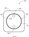
- FIG. 1A is an exemplary diagram of illustrating a front view in accordance with an embodiment of the present invention
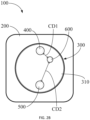
- FIG. 1B is an exemplary diagram illustrating a rear view in accordance with an embodiment of FIG. 1A
- the connector 100 is configured for applying to a battery module, and comprises an insulating body 200, a holder 300 and multiple metal pins.
- the metal pins may have different configuration, at least include a first power terminal 400, a second power terminal 500 and a signal terminal 600.
- the holder 300 is located inside the insulating body 200 which isolates two independent space inside the insulating body 200 defining a front region 310 at a side of holder 300 and a rear region 320 at another side.
- the first creepage distance is defined as a distance between the signal terminal 600 and the first power terminal 400
- the second creepage distance is defined as a distance between the signal terminal 600 and the second power terminal 500
- signal terminal 600 comprising pins of low-level triggered, high-level triggered, high anti-noise and low anti-noise.
- the high-level triggered pin means that the corresponding recipient will be triggered when the received signal is in high-level voltage.
- the low-level triggered pin receives low-level voltage for triggering the recipient.
- the high anti-noise pin means the corresponding recipient is higher capability anti-noise capability, and the low anti-noise pin mean the recipient has weaker resistant capability toward the noise.
- the high-level triggered pin Since the high-level triggered pin is for high-level voltage, if it is too close to the positive pin (i.e., the first power terminal 400), the high-level voltage at the positive pin may affect the high-level triggered pin resulting mis-triggering. Therefore, the high-level triggered pin must be located away the positive pin as far as possible.
- the low-level triggered pin is allowed to near the positive pin but away from the negative pin (i.e., the second power terminal 500) to prevent mis-trigger by the low-level voltage. Similarly, the low anti-noise has less tolerant of noise and thus it must locate far away from the positive pin. Table 1 High-level triggering Low-level triggering High anti-noise ability Less away from the positive pin Less away from the negative pin Low anti-noise ability Must away from the positive pin Must away from the negative pin
- the first creepage distance in order to avoid mis-triggering by the high-level voltage at the positive pin, when the signal terminal is a high-level triggered pin or low anti-noise pin, the first creepage distance must greater than the second creepage distance.
- the second creepage distance in order to avoid mis-triggering by the low-level voltage at the negative pin, when the signal terminal is a low-level triggered pin or high anti-noise pin, the second creepage distance must greater than the first creepage distance.
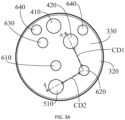
- FIG. 3A an exemplary diagram in accordance with another embodiment of the present invention.
- signals and electricity are transmitting through the connector 100 via multiple pin combination of the first power terminal 400, the second power terminal 400 and the signal terminal 600.
- the first power terminal 400 has a positive charging pin 410 and a positive discharging pin 420.
- the second power terminal 500 has a negative pin for charging and discharging.
- the signal terminal 600 has a low-level triggered pin 630, a high-level triggered pin 610, a pair of high anti-noise pin 640 and a low anti-noise pin 620. These pins are all mounted on the holder 300 that penetrate from the rear region 320 to the front region 310.
- the protruded pins that is exposed in the front region 310 which is configured to engage the corresponding adapter or socket.
- the pins exposed in the rear region 320 are connected to the corresponding cable.
- the rear region 320 filled with insulating gel to ensure the insulation between pins.
- the charging path for the battery module is formed by the positive charging pin 410 and the negative pin 510, and the discharging path of the battery module is formed by the positive discharging pin 420 and the negative pin. It is noted that although the negative pin 50 is a single pin configured for both charging and discharging, the second power terminal 500 may have sperate negative charging pin and the negative discharging pin in another embodiment.
- the high-level triggered pin 610 of the recipient is driven by the high-level voltage, it is easy to be mis-triggered by the high-level voltages of the positive charging pin 410 or discharging pine 320 if the high-level triggered pin 610 is located too close.
- the high-level triggered pin 610 must away from the positive charging pin 410 or discharging pine 320.
- the low-level triggered pin 630 must way from the negative pin 510.
- the numbers of pins may increase due to the needs of the application, the space of the holder may be insufficient to satisfy the above-mentioned arrangement of the creepage distance for the signal terminals 600.
- the low anti-noise pin 620 should place near the negative pin 510 and away from the positive charging pin 410 and the positive discharging pin 420.
- the first creepage distance CD1 of the low anti-noise pin 620 to the positive discharging pin 420 is almost the same to the second creepage distance CD2 of the low anti-noise pin 620 to the negative pin 510.
- a blocking segment 330 is added to increase the first creepage distance CD1.
- the straight line distance (the shortest distance) between the low anti-noise pin 620 and the positive discharging pin 420 is defined as the first distance D1.
- the straight line distance between the low anti-noise pin 620 and the negative pin 510 is defined as the second distance D2.
- the second creepage distance CD2 is the distance of the second distance D2.
- the first creepage distance CD1 is the summation of the first distance D1 and the shortest distance along the surface of the blocking segment. Increasing the first creepage distance CD1 is able to avoid the interfering of the positive discharging pin 420 from mis-trigger.
- the creepage distance of the low anti-noise pin 620 and the positive charging pin 410 already larger than the second creepage distance D2.
- the high-level voltage of the positive charging pin 410 will not take effect of resulting mis-trigger for the low anti-noise pin 620.
- the blocking segment 330 is an independent convex formed inside the rear region 320 of the holder 300.
- the blocking segment inside the rear region 320 may be a convex formed continually along a one side to another side of the holder 300.
- the blocking segment 330 may consisting of multiple independent convex located respectively adjacent to the corresponding signal terminal 600 selectively in between the first power terminal 400 or the second power terminal 500. Furthermore, the blocking segment 330 may be a concave formation. The surface distance P of the concave can also be used to increase the overall creepage distance.
- the high-level triggered terminal 610 may be an Negative Temperature Coefficient (NTC) driven pin.
- the low-level triggered terminal 630 may comprise pins of wakeup and cable detection.
- the high anti-noise terminal 640 may comprise pins of Controller Area Network (CAN) high and CAN low.
- the low anti-noise terminal 620 may comprise pins of transmitting (Tx), receiving (Rx) and single Universal Asynchronous Receiver/Transmitter (UART).
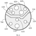
- an insulating gel 700 is filled in the rear region 320 of the holder 300 which covers the first power terminal 400 (i.e., the positive charging pin 410 and the positive discharging pin 420), the second power terminal 500 (i.e., the negative pin 510) and six signal terminal 600 (i.e., the low-level triggered terminal 630, a high-level triggered terminal 610, two high anti-noise terminals 630 and two low anti-noise terminal 620).
- the insulating gel 700 ensures insulations between terminals.
- the connector of the present invention uses proper arrangement of creepage distances based on the predetermined rule to ensure the insulations between terminals, especially the first creepage distance CD1 between the signal terminal 600 and the first power terminal 400 and the second creepage distance CD2 between the signal terminal 600 and the second power terminal 500.
- the present invention also relates to provides a connector that has an insulating body, a holder, at least one first power terminal, at least one second power terminal and at least signal terminal.
- the holder is located inside the insulating body, and has a front region and a rear region corresponded to the front region.
- a first creepage distance is defined in between one of the at least one signal terminal and a first power terminal.
- a second creepage distance is defined in between the one of the at least one signal terminal and a second power terminal.
Landscapes
- Chemical & Material Sciences (AREA)
- Chemical Kinetics & Catalysis (AREA)
- Electrochemistry (AREA)
- General Chemical & Material Sciences (AREA)
- Connector Housings Or Holding Contact Members (AREA)
- Details Of Connecting Devices For Male And Female Coupling (AREA)
Applications Claiming Priority (1)
| Application Number | Priority Date | Filing Date | Title |
|---|---|---|---|
| CN202121629372.2U CN216085410U (zh) | 2021-07-16 | 2021-07-16 | 连接器 |
Publications (1)
| Publication Number | Publication Date |
|---|---|
| EP4191802A1 true EP4191802A1 (de) | 2023-06-07 |
Family
ID=80665857
Family Applications (1)
| Application Number | Title | Priority Date | Filing Date |
|---|---|---|---|
| EP22185322.9A Withdrawn EP4191802A1 (de) | 2021-07-16 | 2022-07-15 | Verbinder |
Country Status (2)
| Country | Link |
|---|---|
| EP (1) | EP4191802A1 (de) |
| CN (1) | CN216085410U (de) |
Citations (6)
| Publication number | Priority date | Publication date | Assignee | Title |
|---|---|---|---|---|
| US5595496A (en) * | 1993-11-10 | 1997-01-21 | Sumitomo Wiring Systems, Ltd. | Water-proof connector |
| CN201584574U (zh) * | 2009-12-09 | 2010-09-15 | 沈阳兴华航空电器有限责任公司 | 一种具有凸凹面绝缘体的高压电连接器 |
| US20140062493A1 (en) * | 2012-09-06 | 2014-03-06 | Johnson Controls Technology Llc | High voltage connector system and method |
| CN212230731U (zh) * | 2020-07-15 | 2020-12-25 | 昆山君磊电器有限公司 | 电连接器及电池充放电系统 |
| US20210194167A1 (en) * | 2019-12-20 | 2021-06-24 | Westinghouse Air Brake Technologies Corporation | Connector assembly |
| CN213692402U (zh) * | 2020-10-23 | 2021-07-13 | 富港电子(徐州)有限公司 | 电连接器组合 |
-
2021
- 2021-07-16 CN CN202121629372.2U patent/CN216085410U/zh active Active
-
2022
- 2022-07-15 EP EP22185322.9A patent/EP4191802A1/de not_active Withdrawn
Patent Citations (6)
| Publication number | Priority date | Publication date | Assignee | Title |
|---|---|---|---|---|
| US5595496A (en) * | 1993-11-10 | 1997-01-21 | Sumitomo Wiring Systems, Ltd. | Water-proof connector |
| CN201584574U (zh) * | 2009-12-09 | 2010-09-15 | 沈阳兴华航空电器有限责任公司 | 一种具有凸凹面绝缘体的高压电连接器 |
| US20140062493A1 (en) * | 2012-09-06 | 2014-03-06 | Johnson Controls Technology Llc | High voltage connector system and method |
| US20210194167A1 (en) * | 2019-12-20 | 2021-06-24 | Westinghouse Air Brake Technologies Corporation | Connector assembly |
| CN212230731U (zh) * | 2020-07-15 | 2020-12-25 | 昆山君磊电器有限公司 | 电连接器及电池充放电系统 |
| CN213692402U (zh) * | 2020-10-23 | 2021-07-13 | 富港电子(徐州)有限公司 | 电连接器组合 |
Also Published As
| Publication number | Publication date |
|---|---|
| CN216085410U (zh) | 2022-03-18 |
Similar Documents
| Publication | Publication Date | Title |
|---|---|---|
| US11069992B2 (en) | Connector part comprising a circuit board | |
| TWI828624B (zh) | 電連接器系統及其使用方法 | |
| EP4024624B1 (de) | Verbinder, verbindungsanordnung und rückwandverbindungssystem | |
| US9437980B2 (en) | Connector | |
| ES2214499T3 (es) | Union universal para interfaces de telefonos celulares. | |
| US7537488B2 (en) | Communication cable connector and communication cable | |
| US6452402B1 (en) | Apparatus for determining the type of external device being connected | |
| US11855373B2 (en) | Connector assembly with a detection system | |
| US5188540A (en) | Hearing aid having electrical contact means arranged in a battery compartment | |
| US20230198105A1 (en) | Electronic component for a cell-contacting system, cell contacting system, and method for producing the cell contacting system or a battery module | |
| US9431769B2 (en) | Electrical connector having improved shielding | |
| EP3709448B1 (de) | Endpositionssicherungselement mit mehreren verriegelungen | |
| KR200485712Y1 (ko) | 복합형 연결 소켓 | |
| EP3703197B1 (de) | Verbinder mit überspannungsschutzfunktion und leiterplatte damit | |
| KR102204858B1 (ko) | 배터리 모듈 | |
| CN219590561U (zh) | 一种光电模块、光电连接器组件及通信单元 | |
| US9240647B2 (en) | Connector and mating connector connectable to the same | |
| CN109273944A (zh) | 电子设备 | |
| CN216085410U (zh) | 连接器 | |
| CN215579392U (zh) | 一种具备接口连接器及吸附装置的机身保护装置 | |
| CN212462169U (zh) | 一种高速传输数字信号d-sub连接器 | |
| EP4407744A1 (de) | Wiederaufladbares batteriepack | |
| EP4178184A1 (de) | Batteriefehlerdetektionsanordnungen | |
| US9531437B1 (en) | Communication line adapter with electromagnetic interference protection | |
| US20170093227A1 (en) | Corrosion resistant optical connector with accompanying circuitry |
Legal Events
| Date | Code | Title | Description |
|---|---|---|---|
| PUAI | Public reference made under article 153(3) epc to a published international application that has entered the european phase |
Free format text: ORIGINAL CODE: 0009012 |
|
| STAA | Information on the status of an ep patent application or granted ep patent |
Free format text: STATUS: THE APPLICATION HAS BEEN PUBLISHED |
|
| AK | Designated contracting states |
Kind code of ref document: A1 Designated state(s): AL AT BE BG CH CY CZ DE DK EE ES FI FR GB GR HR HU IE IS IT LI LT LU LV MC MK MT NL NO PL PT RO RS SE SI SK SM TR |
|
| STAA | Information on the status of an ep patent application or granted ep patent |
Free format text: STATUS: THE APPLICATION IS DEEMED TO BE WITHDRAWN |
|
| 18D | Application deemed to be withdrawn |
Effective date: 20231208 |