EP4191660A1 - Wiring board, package for mounting light-emitting element, and light-emitting device - Google Patents
Wiring board, package for mounting light-emitting element, and light-emitting device Download PDFInfo
- Publication number
- EP4191660A1 EP4191660A1 EP21850243.3A EP21850243A EP4191660A1 EP 4191660 A1 EP4191660 A1 EP 4191660A1 EP 21850243 A EP21850243 A EP 21850243A EP 4191660 A1 EP4191660 A1 EP 4191660A1
- Authority
- EP
- European Patent Office
- Prior art keywords
- resin layer
- insulating resin
- wiring board
- ridge portions
- closed pore
- Prior art date
- Legal status (The legal status is an assumption and is not a legal conclusion. Google has not performed a legal analysis and makes no representation as to the accuracy of the status listed.)
- Withdrawn
Links
Images




Classifications
-
- H—ELECTRICITY
- H10—SEMICONDUCTOR DEVICES; ELECTRIC SOLID-STATE DEVICES NOT OTHERWISE PROVIDED FOR
- H10H—INORGANIC LIGHT-EMITTING SEMICONDUCTOR DEVICES HAVING POTENTIAL BARRIERS
- H10H20/00—Individual inorganic light-emitting semiconductor devices having potential barriers, e.g. light-emitting diodes [LED]
- H10H20/80—Constructional details
- H10H20/85—Packages
- H10H20/857—Interconnections, e.g. lead-frames, bond wires or solder balls
-
- H—ELECTRICITY
- H05—ELECTRIC TECHNIQUES NOT OTHERWISE PROVIDED FOR
- H05K—PRINTED CIRCUITS; CASINGS OR CONSTRUCTIONAL DETAILS OF ELECTRIC APPARATUS; MANUFACTURE OF ASSEMBLAGES OF ELECTRICAL COMPONENTS
- H05K1/00—Printed circuits
- H05K1/02—Details
- H05K1/03—Use of materials for the substrate
- H05K1/05—Insulated conductive substrates, e.g. insulated metal substrate
-
- H—ELECTRICITY
- H05—ELECTRIC TECHNIQUES NOT OTHERWISE PROVIDED FOR
- H05K—PRINTED CIRCUITS; CASINGS OR CONSTRUCTIONAL DETAILS OF ELECTRIC APPARATUS; MANUFACTURE OF ASSEMBLAGES OF ELECTRICAL COMPONENTS
- H05K1/00—Printed circuits
- H05K1/02—Details
- H05K1/03—Use of materials for the substrate
- H05K1/05—Insulated conductive substrates, e.g. insulated metal substrate
- H05K1/056—Insulated conductive substrates, e.g. insulated metal substrate the metal substrate being covered by an organic insulating layer
-
- H—ELECTRICITY
- H10—SEMICONDUCTOR DEVICES; ELECTRIC SOLID-STATE DEVICES NOT OTHERWISE PROVIDED FOR
- H10W—GENERIC PACKAGES, INTERCONNECTIONS, CONNECTORS OR OTHER CONSTRUCTIONAL DETAILS OF DEVICES COVERED BY CLASS H10
- H10W70/00—Package substrates; Interposers; Redistribution layers [RDL]
- H10W70/60—Insulating or insulated package substrates; Interposers; Redistribution layers
-
- H—ELECTRICITY
- H10—SEMICONDUCTOR DEVICES; ELECTRIC SOLID-STATE DEVICES NOT OTHERWISE PROVIDED FOR
- H10W—GENERIC PACKAGES, INTERCONNECTIONS, CONNECTORS OR OTHER CONSTRUCTIONAL DETAILS OF DEVICES COVERED BY CLASS H10
- H10W70/00—Package substrates; Interposers; Redistribution layers [RDL]
- H10W70/60—Insulating or insulated package substrates; Interposers; Redistribution layers
- H10W70/67—Insulating or insulated package substrates; Interposers; Redistribution layers characterised by their insulating layers or insulating parts
- H10W70/68—Shapes or dispositions thereof
- H10W70/6875—Shapes or dispositions thereof being on a metallic substrate, e.g. insulated metal substrates [IMS]
-
- H—ELECTRICITY
- H10—SEMICONDUCTOR DEVICES; ELECTRIC SOLID-STATE DEVICES NOT OTHERWISE PROVIDED FOR
- H10W—GENERIC PACKAGES, INTERCONNECTIONS, CONNECTORS OR OTHER CONSTRUCTIONAL DETAILS OF DEVICES COVERED BY CLASS H10
- H10W70/00—Package substrates; Interposers; Redistribution layers [RDL]
- H10W70/60—Insulating or insulated package substrates; Interposers; Redistribution layers
- H10W70/67—Insulating or insulated package substrates; Interposers; Redistribution layers characterised by their insulating layers or insulating parts
- H10W70/69—Insulating materials thereof
-
- H—ELECTRICITY
- H10—SEMICONDUCTOR DEVICES; ELECTRIC SOLID-STATE DEVICES NOT OTHERWISE PROVIDED FOR
- H10W—GENERIC PACKAGES, INTERCONNECTIONS, CONNECTORS OR OTHER CONSTRUCTIONAL DETAILS OF DEVICES COVERED BY CLASS H10
- H10W90/00—Package configurations
-
- H—ELECTRICITY
- H10—SEMICONDUCTOR DEVICES; ELECTRIC SOLID-STATE DEVICES NOT OTHERWISE PROVIDED FOR
- H10H—INORGANIC LIGHT-EMITTING SEMICONDUCTOR DEVICES HAVING POTENTIAL BARRIERS
- H10H20/00—Individual inorganic light-emitting semiconductor devices having potential barriers, e.g. light-emitting diodes [LED]
- H10H20/80—Constructional details
- H10H20/85—Packages
- H10H20/8506—Containers
-
- H—ELECTRICITY
- H10—SEMICONDUCTOR DEVICES; ELECTRIC SOLID-STATE DEVICES NOT OTHERWISE PROVIDED FOR
- H10H—INORGANIC LIGHT-EMITTING SEMICONDUCTOR DEVICES HAVING POTENTIAL BARRIERS
- H10H20/00—Individual inorganic light-emitting semiconductor devices having potential barriers, e.g. light-emitting diodes [LED]
- H10H20/80—Constructional details
- H10H20/85—Packages
- H10H20/858—Means for heat extraction or cooling
- H10H20/8581—Means for heat extraction or cooling characterised by their material
-
- H—ELECTRICITY
- H10—SEMICONDUCTOR DEVICES; ELECTRIC SOLID-STATE DEVICES NOT OTHERWISE PROVIDED FOR
- H10H—INORGANIC LIGHT-EMITTING SEMICONDUCTOR DEVICES HAVING POTENTIAL BARRIERS
- H10H20/00—Individual inorganic light-emitting semiconductor devices having potential barriers, e.g. light-emitting diodes [LED]
- H10H20/80—Constructional details
- H10H20/85—Packages
- H10H20/858—Means for heat extraction or cooling
- H10H20/8582—Means for heat extraction or cooling characterised by their shape
Definitions
- the present disclosure relates to a wiring board, a light emitting element mounting-use package, and a light emitting device.
- the metal substrate includes a layered insulating layer made of organic resin, forming a wiring board or a light emitting element mounting-use package (see, for example, Patent Document 1).
- Patent Document 1 JP 2013-38452 A
- a wiring board includes a metal substrate, an insulating resin layer positioned on the metal substrate, and an electrical conductor layer positioned on the insulating resin layer.
- the insulating resin layer includes a first surface facing the metal substrate, a second surface positioned opposite to the first surface, third surfaces positioned between the first surface and the second surface, first ridge portions where the first surface meets the third surfaces, and second ridge portions where the second surface meets the third surfaces.
- the insulating resin layer includes a first closed pore group closer to the first ridge portions than to the second ridge portions.
- the first closed pore group includes a plurality of closed pores densely contained.
- a wiring board includes a metal substrate, an insulating resin layer positioned on the metal substrate, and an electrical conductor layer positioned on the insulating resin layer.
- the insulating resin layer includes a first surface facing the metal substrate, a second surface positioned opposite to the first surface, a through hole formed from the first surface to the second surface, fourth surfaces positioned between the first surface and the second surface in the through hole, third ridge portions where the first surface meets the fourth surfaces, and fourth ridge portions where the second surface meets the fourth surfaces.
- the insulating resin layer includes a second closed pore group closer to the third ridge portions than to the fourth ridge portions.
- the second closed pore group includes a plurality of closed pores densely contained.
- a light emitting element mounting-use package includes a submount configured to mount a light emitting element and disposed on the wiring board described above.
- a light emitting device includes a light emitting element provided on the submount of the light emitting element mounting-use package described above.
- the light emitting element mounting-use package disclosed in Patent Document 1 has a structure in which an insulating layer made of organic resin is layered on a metal substrate.
- the metal substrate may be referred to as a substrate.
- the insulating layer made of organic resin may be referred to as an insulating layer.
- the substrate and the insulating layer are made of different materials.
- the substrate is basically less likely to adhere tightly to the insulating layer.
- the insulating layer may be peeled from the substrate. This is due to a large difference in coefficient of thermal expansion between the substrate and the insulating layer.
- the insulating layer is made of organic resin but has high rigidity.
- the insulating layer made of organic resin has a sharply increased Young's modulus at a surrounding temperature lower than a room temperature (25°C). Due to such factors, the light emitting element mounting-use package having the structure in which the insulating layer made of organic resin is layered on the metal substrate causes the insulating layer to be easily peeled from the substrate.
- the present disclosure provides, even in, for example, a structure in which an insulating layer made of organic resin is layered on a metal substrate, a wiring board including the insulating layer less likely to be peeled from the substrate, a light emitting element mounting-use package, and a light emitting device.
- a wiring board, a light emitting element mounting-use package, and a light emitting device of an embodiment will be described in detail below with reference to FIG. 1 to FIG. 9 .
- the present disclosure is not limited to the specific embodiments described below.
- a disclosed aspect will include various aspects, provided that these aspects fall within the spirit or scope of the general inventive concepts as defined by the appended claims.
- FIG. 1 is an exterior perspective view of a wiring board illustrated as an example of an embodiment.
- FIG. 2 is a cross-sectional view taken along line II-II in FIG. 1 .
- FIG. 3 is a cross-sectional view taken along line III-III in FIG. 1 .
- FIG. 4 is an enlarged cross-sectional view of a portion P1 in FIG. 2 .
- a wiring board A illustrated in FIG. 1 includes a metal substrate 1, an insulating resin layer 3, and an electrical conductor layer 5.
- the insulating resin layer 3 is positioned on the metal substrate 1.
- the insulating resin layer 3 is layered on the metal substrate 1.
- the electrical conductor layer 5 is positioned on the insulating resin layer 3 in this case.
- the electrical conductor layer 5 is disposed near an end of a second surface 3b of the insulating resin layer 3, but the position of the electrical conductor layer 5 is not limited to such a position.
- the electrical conductor layer 5 may be disposed in any location required depending on the pattern design. In FIG. 1 , the number of electrical conductor layers 5 is two, but any required number of electrical conductor layers 5 may be disposed.
- the insulating resin layer 3 includes a first surface 3a, the second surface 3b, and third surfaces 3c.
- the first surface 3a is a surface facing the metal substrate 1.
- the second surface 3b is a surface positioned opposite to the first surface 3a.
- the third surfaces 3c are surfaces positioned between the first surface 3a and the second surface 3b.
- the first surface 3a and the second surface 3b are principal surfaces of the insulating resin layer 3.
- the third surfaces 3c are so-called side surfaces of the insulating resin layer 3.
- the third surfaces 3c have a direction meeting the first surface 3a or the second surface 3b. In FIG. 1 , the third surfaces 3c have a direction perpendicular to the first surface 3a and the second surface 3b but the direction is not limited to the perpendicular direction.
- the wiring board A illustrated in FIG. 1 includes four third surfaces 3c.
- the insulating resin layer 3 includes first ridge portions 3d and second ridge portions 3e.
- the first ridge portions 3d are at positions where the first surface 3a meets the third surfaces 3c.
- the second ridge portions 3e are at positions where the second surface 3b meets the third surfaces 3c.
- the first ridge portions 3d are ridge lines closer to the metal substrate 1 than the second ridge portions 3e is.
- the first ridge portions 3d are disposed surrounding the first surface 3a of the insulating resin layer 3.
- the second ridge portions 3e are disposed surrounding the second surface 3b of the insulating resin layer 3.
- the insulating resin layer 3 includes a large number of closed pores 7a.
- the insulating resin layer 3 includes part where a plurality of closed pores of a large number of the closed pores 7a is densely contained.
- the part where a plurality of closed pores 7a is densely contained is hereinafter referred to as a closed pore group.
- the closed pore group in the insulating resin layer 3 of the wiring board A is referred to as a first closed pore group 7.
- a state with the plurality of closed pores 7a densely contained is referred to as a state where the number of closed pores 7a in a predetermined volume is larger than that in other regions. In this case, the volume may be replaced with a predetermined cross sectional area (unit area) of the insulating resin layer 3. As illustrated in FIG.
- the unit area is referred to as a circular region that can be drawn by simply connecting contours of the plurality of closed pores 7a positioned at the outermost periphery in the part where the plurality of closed pores is densely contained.
- the porosity of the first closed pore group 7 per unit area is preferably not less than 50%.
- the porosity of the first closed pore group is roughly up to 80%.
- the first closed pore group 7 is closer to the first ridge portions 3d than the second ridge portions 3e of the insulating resin layer 3 is. In other words, the first closed pore group 7 is near the first ridge portions 3d in the insulating resin layer 3. More specifically, the first closed pore group 7 is near the outer peripheral edge of the first surface 3a in the insulating resin layer 3.
- the region including the first closed pore group 7 has a proportion of resin forming the insulating resin layer 3 lower than other regions in the insulating resin layer 3.
- the elastic modulus in the region including the first closed pore group 7 in the insulating resin layer 3 is lower than that in other regions in the insulating resin layer 3.
- part where the elastic modulus is lower than that in other regions is formed near the first ridge portions 3d of the insulating resin layer 3. This can reduce stress produced between the metal substrate 1 and the insulating resin layer 3. As a result, the probability of peeling between the metal substrate 1 and the insulating resin layer 3 can be reduced.
- the likelihood that the insulating resin layer 3 is peeled from the metal substrate 1 can be reduced.
- the insulating resin layer 3 is likely to be peeled from peripheral edges 3co.
- the insulating resin layer 3 is particularly likely to be peeled from its corner portions 3coc.
- the wiring board A includes the first closed pore group 7 near the first ridge portions 3d in the insulating resin layer 3.
- Part including the first closed pore group 7 in the insulating resin layer 3 has a low elastic modulus.
- the part including the first closed pore group 7 is likely to be deformed.
- fixing strength to a surface 1a of the metal substrate 1 improves.
- the part including the first closed pore group 7 is a part near the surface 1a of the metal substrate 1 in a thickness direction of the insulating resin layer 3, and is near the peripheral edges 3co of the insulating resin layer 3 in plan view of the insulating resin layer 3.
- other regions are regions farther from the surface 1a of the metal substrate 1 in the thickness direction of the insulating resin layer 3 than the region including the first closed pore group 7 is and are near a center 3 cc than to the peripheral edges 3co of the insulating resin layer 3 in plan view of the insulating resin layer 3 as illustrated in FIG. 2 and FIG. 3 .
- the first closed pore group 7 includes the plurality of closed pores 7a.
- the closed pores 7a are air holes inside the insulating resin layer 3.
- the closed pores 7a have a closed space.
- the closed pores 7a do not face the first surface 3a, the second surface 3b, the side surfaces (third surfaces 3c), or the first ridge portions 3d of the insulating resin layer 3.
- the closed pores 7a have no portion open to the first surface 3a, the second surface 3b, the side surfaces (third surfaces 3c), or the first ridge portions 3d of the insulating resin layer 3.
- a closed pore 7a is independently included in the insulating resin layer 3.
- the closed pores 7a forming the first closed pore group 7 have a larger average diameter than the closed pores 7a included in the regions other than the part of the first closed pore group 7.
- An average diameter D1 of the closed pores 7a forming the first closed pore group 7 may be from 1.5 to 5 times as large as an average diameter D2 of the closed pores 7a included in the region other than the part of the first closed pore group 7.
- the region including the first closed pore group 7 is identified from a large number of the closed pores 7a included in the insulating resin layer 3 as follows. First, a cross section as illustrated in FIG. 3 is extracted from the wiring board A. Next, the cross section is observed using, for example, an electron microscope to identify the existence of the closed pores 7a from the photograph. Next, a candidate for the first closed pore group 7 as part where the closed pores 7a are densely contained is located, and tentative separation from a region where the closed pores 7a are not densely contained is visually performed.
- the diameter of each of the closed pores 7a is obtained through image analysis of the part as the candidate for the first closed pore group 7.
- the diameter of each of the closed pores 7a is obtained by converting the area of the closed pores 7a obtained through the image analysis into the area of a circle. From a measurement value of the diameter of each of the closed pores 7a obtained, a range including the closed pores 7a having a larger diameter than a threshold is regarded as the range of the first closed pore group 7.
- the threshold of the diameter of the closed pores 7a is 0.05 ⁇ m.
- a closed pore 7a having a diameter smaller than 0.05 ⁇ m is present among the closed pores 7a forming the first closed pore group 7, such a closed pore 7a having a small diameter is also included in the range of the first closed pore group 7. Closed pores 7a having a diameter of not more than 0.01 ⁇ m are excluded, and the diameter is not measured. In this manner, the first closed pore group 7 including the plurality of closed pores 7a densely contained is determined.
- the metal substrate 1 uses one selected from the group including copper, aluminum, an alloy of copper and aluminum, a clad material with a copper plate and an aluminum plate sticked together, or the like.
- a thermosetting resin is suitable for the material of the insulating resin layer 3. Epoxy resin is suitably used as the thermosetting resin.
- the insulating resin layer 3 may include inorganic particles. Copper foil is suitably used as the electrical conductor layer 5.
- FIG. 5 is an exterior perspective view of another aspect of a wiring board.
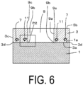
- FIG. 6 is a cross-sectional view taken along line VI-VI in FIG. 5 .
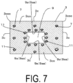
- FIG. 7 is a cross-sectional view taken along line VII-VII in FIG. 5 .
- FIG. 8 is an enlarged cross-sectional view of a portion P2 in FIG. 6 .
- a wiring board B illustrated in FIG. 5 includes the metal substrate 1, the insulating resin layer 3, and the electrical conductor layer 5.
- the insulating resin layer 3 is positioned on the metal substrate 1.
- the electrical conductor layer 5 is positioned on the insulating resin layer 3.
- the electrical conductor layer 5 is disposed near an end of the second surface 3b of the insulating resin layer 3, but the position of the electrical conductor layer 5 is not limited to such a position.
- the electrical conductor layer 5 is disposed in a location required depending on the pattern design. In FIG. 5 , the number of electrical conductor layers 5 is two, but the number of electrical conductor layers 5 required depending on the pattern design may be disposed.
- the insulating resin layer 3 includes the first surface 3a and the second surface 3b.
- the insulating resin layer 3 includes a through hole 9.
- the wiring board B illustrated in FIG. 5 is different from the wiring board A described above in that the insulating resin layer 3 includes the through hole 9.
- the through hole 9 is formed penetrating through the insulating resin layer 3 between the first surface 3a and the second surface 3b.
- the through hole 9 includes inner surfaces 9a.
- the inner surfaces 9a are positioned between the first surface 3a and the second surface 3b of the insulating resin layer 3.
- the through hole 9 illustrated in FIG. 5 has a rectangular shape in plan view.
- the inner surfaces 9a of the through hole 9 include four surfaces.
- One of the inner surfaces 9a of the through hole 9 is referred to as a fourth surface 9aa.
- the inner surfaces 9a of the through hole 9 illustrated in FIG. 5 include four fourth surfaces 9aa.
- the fourth surfaces 9aa all have a direction meeting the first surface 3a.
- the fourth surface 9aa of the four fourth surfaces 9aa will be focused on and described.
- the fourth surface 9aa is positioned between the first surface 3a and the second surface 3b of the insulating resin layer 3.
- the insulating resin layer 3 includes third ridge portions 9b and fourth ridge portions 9c.
- the third ridge portions 9b are portions where the first surface 3a and the fourth surface 9aa of the insulating resin layer 3 meet each other.
- the fourth ridge portions 9c are portions where the second surface 3b and the fourth surface 9aa of the insulating resin layer 3 meet each other.
- the insulating resin layer 3 forming the wiring board B also includes a large number of closed pores as in the wiring board A.
- the insulating resin layer 3 forming the wiring board B also includes a closed pore group having the same configuration as the wiring board A.
- a closed pore group near the through hole 9 formed in the insulating resin layer 3 is referred to as a second closed pore group 11.
- a closed pore group near the through hole 9 formed in the insulating resin layer 3 is referred to as a second closed pore group 11.
- a closed pore group 11 is denoted by a reference numeral 11a.
- the second closed pore group 11 and the closed pores 11a and the first closed pore group 7 and the closed pores 7a are denoted by respective reference numerals for the sake of description.
- the second closed pore group 11 and the closed pores 11a may have the same size and distribution state as the first closed pore group 7 and the closed pores 7a.
- the second closed pore group 11 is closer to the third ridge portions 9b than to the fourth ridge portions 9c of the insulating resin layer 3.
- the second closed pore group 11 is near the third ridge portions 9b in the insulating resin layer 3.
- the region including the second closed pore group 11 has a proportion of resin forming the insulating resin layer 3 lower than other regions in the insulating resin layer 3.
- the elastic modulus in the region including the second closed pore group 11 in the insulating resin layer 3 is lower than that in other regions of the insulating resin layer 3.
- part where the elastic modulus is lower than that in other regions is formed near the third ridge portions 9b of the insulating resin layer 3. This can reduce stress produced between the metal substrate 1 and the insulating resin layer 3.
- the probability of peeling between the insulating resin layer 3 on the through hole 9 side and the metal substrate 1 can be reduced.
- the likelihood that the through hole 9 side of the insulating resin layer 3 is peeled from the metal substrate 1 can be reduced.
- the insulating resin layer 3 is likely to be partially peeled on the inner surface 9a of the through hole 9, which is an end surface the same as the peripheral edges 3co.
- the wiring board B includes the second closed pore group 11 near the third ridge portions 9b in the insulating resin layer 3.
- the peeling of the insulating resin layer 3 from the inner surface 9a side of the through hole 9 can also be reduced.
- Part including the second closed pore group 11 in the insulating resin layer 3 has a low elastic modulus.
- the a part including the second closed pore group 11 is likely to be deformed.
- fixing strength to the surface 1a of the metal substrate 1 improves.
- the part including the second closed pore group 11 is part near the surface 1a of the metal substrate 1 in the thickness direction of the insulating resin layer 3, and near the inner surface 9a of the through hole 9 in plan view of the insulating resin layer 3.
- other regions are regions farther from the surface 1a of the metal substrate 1 in the thickness direction of the insulating resin layer 3 than the region including the second closed pore group 11 is, and are near the peripheral edges 3co from the inner surface 9a of the through hole 9 in plan view of the insulating resin layer 3 as illustrated in FIG. 5 and FIG. 6 .
- the second closed pore group 11 includes the plurality of closed pores 11a.
- the closed pores 11a are air holes inside the insulating resin layer 3.
- the closed pores 11a have a closed space.
- the closed pores 11a do not face the first surface 3a, the second surface 3b, the fourth surfaces 9aa, the side surfaces (third surfaces 3c), the first ridge portions 3d, the second ridge portions 3e, or the third ridge portions 9b of the insulating resin layer 3, and resin is provided between the closed pores 11a and the outside of these portions.
- the closed pores 11a have no portion open to the first surface 3a, the second surface 3b, the fourth surfaces 9aa, the side surfaces (third surfaces 3c), the first ridge portions 3d, the second ridge portions 3e, or the third ridge portions 9b of the insulating resin layer 3.
- a closed pore 11a is independently included in the insulating resin layer 3.
- the closed pores 11a forming the second closed pore group 11 have a larger average diameter than the closed pores 11a included in the regions other than the part of the second closed pore group 11.
- An average diameter D3 of the closed pores 11a forming the second closed pore group 11 may be from 1.5 to 5 times as large as an average diameter D4 of the closed pores 11a included in the region other than the part of the second closed pore group 11.
- the wiring board B may include the first closed pore group 7 in the insulating resin layer 3.
- the wiring board B may include the first closed pore group 7 and the second closed pore group 11 in the insulating resin layer 3.
- the insulating resin layer 3 forming the wiring board B may include, near the first ridge portions 3d, the first closed pore group 7 including the plurality of closed pores 7a densely contained.
- the wiring board B includes the first closed pore group 7 near the first ridge portions 3d in addition to the second closed pore group 11 near the third ridge portions 9b, the peeling of the insulating resin layer 3 layered on the metal substrate 1 not only from the inner surface 9a side of the through hole 9 but also from the peripheral edges 3co and the corner portions 3coc of the insulating resin layer 3 can be reduced.
- the first closed pore group 7 may be positioned throughout the first ridge portions 3d.
- the entirety of the insulating resin layer 3 is less likely to be peeled from the metal substrate 1.
- the second closed pore group 11 may be positioned throughout the third ridge portions 9b.
- the entirety of the fourth surfaces 9aa of the through hole 9 formed in the insulating resin layer 3 is less likely to be peeled from the metal substrate 1.
- being positioned throughout a region means that, as illustrated in FIG. 4 , a maximum length L of the first closed pore group 7 is 1 and that the first closed pore group 7 is disposed along the first ridge portions 3d at a pitch of not more than 10 times as long as the maximum length L of the first closed pore group 7.
- the second closed pore group 11 is disposed along the third ridge portions 9b.
- the insulating resin layer 3 may include a plurality of inorganic particles.
- the plurality of inorganic particles preferably has a particle size distribution having two peaks.
- the particle size distribution of the inorganic particles included in the insulating resin layer 3 has two peaks, a structure in which the inorganic particles with a small diameter are contained between the inorganic particles with a large diameter included in the insulating resin layer 3 can be formed.
- the insulating resin layer 3 having high strength in spite of a low volume ratio of the inorganic particles in the insulating resin layer 3 can be obtained.
- the insulating resin layer 3 can improve adhesive strength to the metal substrate 1.
- the regions of the first closed pore group 7 and the second closed pore group 11 in the insulating resin layer 3 have a high volume ratio of a gap and thus have the low volume ratio of inorganic particles.
- the stress relaxation effect due to the presence of the first closed pore group 7 and the second closed pore group 11 in the insulating resin layer 3 can be maintained.
- the particle size distribution of the inorganic particles having two peaks means that two peaks can simply be observed when the particle size distribution of the inorganic particles is measured and graphed.
- the foot extending from a peak of the inorganic particles having a small particle diameter may overlap the foot extending from a peak of the inorganic particles having a large particle diameter.
- FIG. 9 is a schematic cross-sectional view of a light emitting device D illustrated as an example of the embodiment.
- the light emitting device D illustrated in FIG. 9 includes a light emitting element mounting-use package C and a light emitting element 13.
- Examples of the light emitting element 13 include laser diodes (LD) in addition to LED elements.
- LD laser diodes
- the light emitting element mounting-use package C illustrated in FIG. 9 is based on the wiring board B illustrated in FIG. 6 .
- the light emitting element mounting-use package C includes the wiring board B, a submount substrate 15, and a bonding material 17.
- the submount substrate 15 is fit into the through hole 9 formed in the insulating resin layer 3 forming the wiring board B.
- the submount substrate 15 is disposed on the metal substrate 1 forming the wiring board B.
- the bonding material 17 is disposed on the metal substrate 1 and in the through hole 9 formed in the insulating resin layer 3 forming the wiring board B.
- the bonding material 17 bonds the metal substrate 1 to the submount substrate 15.
- the submount substrate 15 preferably has properties including high thermal conductivity, high strength, high toughness, and low thermal expansion.
- a ceramic is preferably used for the submount substrate 15.
- a ceramic including silicon nitride as a main component is preferably used.
- Solder, Au-Sn, and the like are preferably used for the bonding material 17.
- the submount substrate 15, the metal substrate 1, and the insulating resin layer 3 may have a different coefficient of thermal expansion.
- the light emitting element mounting-use package C When the light emitting element 13 mounted on the light emitting element mounting-use package C operates continuously or discontinuously, the light emitting element mounting-use package C generates heat due to the operation of the light emitting elements 13.
- the metal substrate 1 and the insulating resin layer 3 bonded to each other have a different coefficient of thermal expansion and Young's modulus, thus producing thermal stress therebetween.
- the insulating resin layer 3 of the wiring board B forming the light emitting element mounting-use package C includes the second closed pore group 11 as described above.
- the insulating resin layer 3 is less likely to be peeled from the metal substrate 1 even when the thermal stress is produced between the metal substrate 1 and the insulating resin layer 3.
- the light emitting device D or the light emitting element mounting-use package C having high reliability can be obtained.
- the light emitting device D having high reliability can be similarly obtained when the wiring board A is used for the light emitting element mounting-use package C.
- the submount substrate 15 is disposed on the second surface 3b of the insulating resin layer 3 of the wiring board A.
- the submount substrate 15 is disposed on the second surface 3b of the insulating resin layer 3 with the bonding material 17 in between.
- FIG. 10A and FIG. 10B illustrate part of a manufacturing process of the wiring board A.
- FIG. 10A is a cross-sectional view illustrating a laminate body before pressurizing and heating treatment.
- FIG. 10B is a cross-sectional view illustrating the laminate body after pressurizing and heating treatment.
- the metal plate 21 is a material for obtaining the metal substrate 1.
- the organic resin sheet 23 is a material for obtaining the insulating resin layer 3.
- the metal plate 21 and the organic resin sheet 23 are each machined into a predetermined shape. It is preferable to use a mechanical cutting machine such as one that performs dicing in order to machine the metal plate.
- Thermosetting resin is preferably used for a material of the organic resin sheet 23. Epoxy resin is preferably used as a material of the thermosetting resin. A hardener may be added to the thermosetting resin.
- the organic resin sheet 23 may include inorganic particles. Silica, alumina, and the like are preferably used as the inorganic particles. In this case, the inorganic particles preferably have two peaks in the particle size distribution measured.
- thermosetting resin is cured at a temperature higher than the temperature at which the thermosetting resin used is curable as a curing condition of the thermosetting resin.
- the epoxy resin is cured at approximately 200°C.
- the curing temperature is set to a temperature higher than this temperature by 10°C or higher and 60°C or lower.
- the bubbles 27 are likely to be released from a surface of the organic resin sheet 23 not in contact with the metal plate 21 but are less likely to be released from a surface 23a facing the metal plate 21. This is because the bubbles 27 that are supposed to be released from the organic resin sheet 23 are blocked by the metal plate 21 due to the surface 23a of the organic resin sheet 23 in contact with the metal plate 21. Thus, the bubbles 27 are likely to accumulate near the surface 23a of the organic resin sheet 23 facing the metal plate 21.
- the bubbles 27 dispersed in the organic resin sheet 23 will concentrate near the surface 23a facing the metal plate 21.
- the ratio of the open pores on the surface of the insulating resin layer 3 can be reduced.
- a film sheet with open pores is layered on the surface of the organic resin sheet 23 opposite to the metal plate 21.
- the bubbles 27 originally included in the organic resin sheet 23 move toward, during a first stage of the pressurizing and heating treatment, part of the organic resin sheet 23 that is not in contact with the metal plate 21 and is open.
- the part of the organic resin sheet 23 that is open is, for example, a side surface 23b of the organic resin sheet 23.
- the first closed pore group 7 including the plurality of closed pores densely contained is formed in the insulating resin layer 3 formed by curing the organic resin sheet 23.
- the first closed pore group 7 is formed in a region near the side surfaces (third surfaces 3c) of the insulating resin layer 3 and near the metal plate 21.
- the organic resin sheet 23 has a simple plate shape, and thus the bubbles 27 included in the organic resin sheet 23 concentrate in a region near the side surface 23b of the organic resin sheet 23.
- the wiring board A includes the first closed pore group 7 that is closer to the first ridge portions 3d than to the second ridge portions 3e of the insulating resin layer 3 and includes the plurality of closed pores 7a densely contained.
- the holding time is short, the dissolution of part of the resin component does not proceed, and thus the surface is less likely to be flat.
- the curing temperature is set to around the normal temperature (200°C for example) described above, the insulating resin layer 3 is likely to have an uneven surface, and open pores are likely to be formed. This is because the resin component is less likely to dissolve during the pressurizing and heating.
- FIG. 11A and FIG. 11B illustrate part of a manufacturing process of the wiring board B.
- FIG. 11A is a cross-sectional view illustrating a laminate body before pressurizing and heating treatment.
- FIG. 11B is a cross-sectional view illustrating the laminate body after pressurizing and heating treatment.
- the organic resin sheet 23 forms a hole 29, which will be the through hole 9 of the insulating resin layer 3.
- the hole 29 is formed using a laser beam machine in addition to a mold.
- the hole 29 is formed in the organic resin sheet 23, and thus the bubbles 27 also concentrate in a region near an inner surface 29a of the hole 29. As illustrated in FIG.
- the bubbles 27 concentrate both in the region near the side surface 23b of the organic resin sheet 23 and in the region near the inner surface 29a of the hole 29.
- the wiring board B includes the second closed pore group 11 that is closer to the third ridge portions 9b than to the fourth ridge portions 9c of the through hole 9 formed in the insulating resin layer 3 and includes the plurality of closed pores densely contained.
- the third ridge portions 9b are positioned away from the metal substrate 1, and the fourth ridge portions 9c are positioned near the metal substrate 1.
- the bubbles 27 concentrate at the position as in the wiring board A at this time, also forming the first closed pore group 7.
- a film sheet with open pores is layered on the surface of the organic resin sheet 23 opposite to the metal plate 21.
- the bonding material 17 is disposed in the through hole 9 of the wiring board B produced.
- the submount substrate 15 is disposed on the upper surface of the bonding material 17, and a heating treatment is performed.
- the light emitting element 13 is mounted on the surface of the submount substrate 15. The light emitting element 13 is electrically connected by a bonding wire to the electrical conductor layer 5 provided on the second surface 3b of the insulating resin layer 3 forming the wiring board B.
- the light emitting device D can be obtained.
- the wiring board was produced and reliability was evaluated.
- the wiring board B was produced as the wiring board.
- Aluminum was used for the metal substrate.
- the organic resin sheet to be the insulating resin layer was produced by mixing epoxy resin and silica particles. The content of the silica particles was 30% by volume.
- For the silica particles two types of raw materials were used, one with two peaks in the particle size distribution and one with one peak in the particle size distribution. In addition, 1 part by mass of a curing agent (dicyandiamide) was added to 100 parts by mass of the epoxy resin.
- the through hole of the insulating resin layer was formed using a mold.
- the electrical conductor layer was formed by an electrolytic plating method using a plating solution of nickel containing zinc.
- Table 1 lists conditions for pressurizing and heating in producing the laminate body.
- a film sheet with open pores was layered on a surface of the insulating resin layer opposite to the metal substrate.
- the size of the wiring board produced is as follows.
- the area of the flat surface of the metal substrate and the insulating resin layer is 40 mm ⁇ 40 mm.
- the area of the through hole provided in the insulating resin layer is 20 mm ⁇ 20 mm.
- the thickness of the metal substrate is 2 mm.
- the thickness of the insulating resin layer is 0.2 mm.
- the following evaluations were performed on the produced sample.
- the evaluation items are: presence or absence of the first closed pore group and the second closed pore group formed in the insulating resin layer; presence or absence of peeling of the insulating resin layer from the metal substrate; presence or absence of a crack produced in the insulating resin layer; and the adhesive strength of the insulating resin layer to the metal substrate.
- Presence or absence of the first closed pore group and the second closed pore group formed in the insulating resin layer was confirmed as follows. First, a cross section as illustrated in FIG. 3 was obtained from the wiring board produced. Next, for example, the cross section was observed using a scanning electron microscope, to check where closed pores were in the photograph. Next, a candidate for the first closed pore group and the second closed pore group as part where the closed pores were densely contained was located, and tentative separation from a region where the closed pores were not densely contained was visually performed. Next, the diameter of each of the closed pores was obtained through image analysis of the part as the candidate for the first closed pore group and the second closed pore group.
- the diameter of each of the closed pores was obtained by converting the area of the closed pores obtained through the image analysis into the area of a circle. From a measurement value of the diameter of each of the closed pores obtained, a range including the closed pores having a larger diameter than a threshold was regarded as the ranges of the first closed pore group and the second closed pore group. A threshold of the diameter of the closed pores was 0.05 ⁇ m. When a closed pore having a diameter smaller than 0.05 ⁇ m is present among the closed pores forming the first closed pore group and the second closed pore group, such a closed pore having a small diameter was also included in the region of the first closed pore group and the second closed pore group.
- the closed pores with a diameter that was not more than 0.01 ⁇ m were not subjected to the measurement, that is, excluded from the measurement target. It was confirmed that the second closed pore group was formed closer to the third ridge portions than to the fourth ridge portions in the insulating resin layer in the wiring board produced. It was also confirmed that the second closed pore group was formed over the entire circumference of the inner walls (inner surfaces) formed by the four surfaces (fourth surfaces) forming the through hole. The porosity of each of the first closed pore group and the second closed pore group was not less than 50%. In this case, the maximum porosity of the first closed pore group and the second closed pore group was 70%.
- Presence or absence of peeling of the insulating resin layer from the metal substrate was evaluated using a method of immersion in a soldering pot set to 300°C for 30 seconds.
- Presence or absence of a crack produced in the insulating resin layer was confirmed using a method of checking after a temperature cycle test.
- the conditions for the temperature cycle test were that the minimum temperature was -55°C, the maximum temperature was 150°C, and the holding time at the minimum temperature, the holding time at the maximum temperature, and the time for changing the temperature from the minimum temperature to the maximum temperature or vice versa were each 15 minutes.
- the number of temperature cycles was set to 3000.
- a state in which the insulating resin layer was peeled or cracked was confirmed by a method of immersion in a red check liquid. Samples in which ingress of the red check liquid into the insulating resin layer was observed were determined to be defective. At the same time, the ingress of the red check liquid into between the metal substrate and the insulating resin layer was also evaluated.
- the adhesive strength of the insulating resin layer to the metal substrate was measured using a tensile tester (autograph). The evaluations were each performed with the number of samples being 10. In this case, when peeling or a crack was found in at least one of the evaluated samples (10 samples), the sample was evaluated as "Present”. An average value was determined for the adhesive strength. [Table 1] Sample No.
- the adhesive strength of the insulating resin layer to the metal substrate was 1.1 MPa lower than in the sample No. 1, and a crack was found in the insulating resin layer.
- the adhesive strength of the insulating resin layer to the metal substrate was 1.5 MPa lower than in the sample No. 1, and a crack was found in the insulating resin layer. Note that the cracks found in samples Nos. 2 and 3 had a size small enough not to compromise the performance of the wiring board.
Landscapes
- Engineering & Computer Science (AREA)
- Microelectronics & Electronic Packaging (AREA)
- Insulated Metal Substrates For Printed Circuits (AREA)
- Production Of Multi-Layered Print Wiring Board (AREA)
- Led Device Packages (AREA)
Abstract
Description
- The present disclosure relates to a wiring board, a light emitting element mounting-use package, and a light emitting device.
- In recent years, light emitting diodes (LEDs) and laser diodes (LDs) have been used in headlamps of automobiles. Light source devices using these semiconductor elements are required to have high heat dissipation. In view of this, a metal substrate is used for the light source devices. The metal substrate includes a layered insulating layer made of organic resin, forming a wiring board or a light emitting element mounting-use package (see, for example, Patent Document 1).
- Patent Document 1:
JP 2013-38452 A - A wiring board according to the present disclosure includes a metal substrate, an insulating resin layer positioned on the metal substrate, and an electrical conductor layer positioned on the insulating resin layer. The insulating resin layer includes a first surface facing the metal substrate, a second surface positioned opposite to the first surface, third surfaces positioned between the first surface and the second surface, first ridge portions where the first surface meets the third surfaces, and second ridge portions where the second surface meets the third surfaces. The insulating resin layer includes a first closed pore group closer to the first ridge portions than to the second ridge portions. The first closed pore group includes a plurality of closed pores densely contained.
- A wiring board according to the present disclosure includes a metal substrate, an insulating resin layer positioned on the metal substrate, and an electrical conductor layer positioned on the insulating resin layer. The insulating resin layer includes a first surface facing the metal substrate, a second surface positioned opposite to the first surface, a through hole formed from the first surface to the second surface, fourth surfaces positioned between the first surface and the second surface in the through hole, third ridge portions where the first surface meets the fourth surfaces, and fourth ridge portions where the second surface meets the fourth surfaces. The insulating resin layer includes a second closed pore group closer to the third ridge portions than to the fourth ridge portions. The second closed pore group includes a plurality of closed pores densely contained.
- A light emitting element mounting-use package according to the present disclosure includes a submount configured to mount a light emitting element and disposed on the wiring board described above.
- A light emitting device according to the present disclosure includes a light emitting element provided on the submount of the light emitting element mounting-use package described above.
-
-
FIG. 1 is an exterior perspective view of a wiring board illustrated as an example of an embodiment. -
FIG. 2 is a cross-sectional view taken along line II-II inFIG. 1 . -
FIG. 3 is a cross-sectional view taken along line III-III inFIG. 1 . -
FIG. 4 is an enlarged cross-sectional view of a portion P1 inFIG. 2 . -
FIG. 5 is an exterior perspective view of another aspect of a wiring board. -
FIG. 6 is a cross-sectional view taken along line VI-VI inFIG. 5 . -
FIG. 7 is a cross-sectional view taken along line VII-VII inFIG. 5 . -
FIG. 8 is an enlarged cross-sectional view of a portion P2 inFIG. 6 . -
FIG. 9 is a schematic cross-sectional view of a light emitting device illustrated as an example of an embodiment. -
FIG. 10A is a cross-sectional view illustrating a laminate body before pressurizing and heating treatment, which is part of a manufacturing process for a wiring board A. -
FIG. 10B is a cross-sectional view illustrating the laminate body after the pressurizing and heating treatment, which is part of the manufacturing process for the wiring board A. -
FIG. 11A is a cross-sectional view illustrating a laminate body before pressurizing and heating treatment, which is part of a manufacturing process for a wiring board B. -
FIG. 11B is a cross-sectional view illustrating the laminate body after the pressurizing and heating, which is part of the manufacturing process for the wiring board B. - The light emitting element mounting-use package disclosed in
Patent Document 1 has a structure in which an insulating layer made of organic resin is layered on a metal substrate. Hereinafter, the metal substrate may be referred to as a substrate. The insulating layer made of organic resin may be referred to as an insulating layer. The substrate and the insulating layer are made of different materials. Thus, the substrate is basically less likely to adhere tightly to the insulating layer. For example, when the light emitting element mounting-use package is exposed to a sharp change in temperature, the insulating layer may be peeled from the substrate. This is due to a large difference in coefficient of thermal expansion between the substrate and the insulating layer. The insulating layer is made of organic resin but has high rigidity. The insulating layer made of organic resin has a sharply increased Young's modulus at a surrounding temperature lower than a room temperature (25°C). Due to such factors, the light emitting element mounting-use package having the structure in which the insulating layer made of organic resin is layered on the metal substrate causes the insulating layer to be easily peeled from the substrate. - The present disclosure provides, even in, for example, a structure in which an insulating layer made of organic resin is layered on a metal substrate, a wiring board including the insulating layer less likely to be peeled from the substrate, a light emitting element mounting-use package, and a light emitting device.
- A wiring board, a light emitting element mounting-use package, and a light emitting device of an embodiment will be described in detail below with reference to
FIG. 1 to FIG. 9 . Note that the present disclosure is not limited to the specific embodiments described below. Also, a disclosed aspect will include various aspects, provided that these aspects fall within the spirit or scope of the general inventive concepts as defined by the appended claims. -
FIG. 1 is an exterior perspective view of a wiring board illustrated as an example of an embodiment.FIG. 2 is a cross-sectional view taken along line II-II inFIG. 1 .FIG. 3 is a cross-sectional view taken along line III-III inFIG. 1 .FIG. 4 is an enlarged cross-sectional view of a portion P1 inFIG. 2 . - A wiring board A illustrated in
FIG. 1 includes ametal substrate 1, aninsulating resin layer 3, and anelectrical conductor layer 5. Theinsulating resin layer 3 is positioned on themetal substrate 1. Theinsulating resin layer 3 is layered on themetal substrate 1. Theelectrical conductor layer 5 is positioned on theinsulating resin layer 3 in this case. InFIG. 1 , theelectrical conductor layer 5 is disposed near an end of asecond surface 3b of theinsulating resin layer 3, but the position of theelectrical conductor layer 5 is not limited to such a position. Theelectrical conductor layer 5 may be disposed in any location required depending on the pattern design. InFIG. 1 , the number ofelectrical conductor layers 5 is two, but any required number ofelectrical conductor layers 5 may be disposed. - The
insulating resin layer 3 includes afirst surface 3a, thesecond surface 3b, andthird surfaces 3c. Thefirst surface 3a is a surface facing themetal substrate 1. Thesecond surface 3b is a surface positioned opposite to thefirst surface 3a. The third surfaces 3c are surfaces positioned between thefirst surface 3a and thesecond surface 3b. Thefirst surface 3a and thesecond surface 3b are principal surfaces of the insulatingresin layer 3. The third surfaces 3c are so-called side surfaces of the insulatingresin layer 3. The third surfaces 3c have a direction meeting thefirst surface 3a or thesecond surface 3b. InFIG. 1 , thethird surfaces 3c have a direction perpendicular to thefirst surface 3a and thesecond surface 3b but the direction is not limited to the perpendicular direction. The wiring board A illustrated inFIG. 1 includes fourthird surfaces 3c. - The insulating
resin layer 3 includesfirst ridge portions 3d andsecond ridge portions 3e. Thefirst ridge portions 3d are at positions where thefirst surface 3a meets the third surfaces 3c. Thesecond ridge portions 3e are at positions where thesecond surface 3b meets the third surfaces 3c. Thefirst ridge portions 3d are ridge lines closer to themetal substrate 1 than thesecond ridge portions 3e is. InFIG. 1 , thefirst ridge portions 3d are disposed surrounding thefirst surface 3a of the insulatingresin layer 3. InFIG. 1 , thesecond ridge portions 3e are disposed surrounding thesecond surface 3b of the insulatingresin layer 3. - The insulating
resin layer 3 includes a large number ofclosed pores 7a. The insulatingresin layer 3 includes part where a plurality of closed pores of a large number of theclosed pores 7a is densely contained. The part where a plurality ofclosed pores 7a is densely contained is hereinafter referred to as a closed pore group. The closed pore group in the insulatingresin layer 3 of the wiring board A is referred to as a firstclosed pore group 7. A state with the plurality ofclosed pores 7a densely contained is referred to as a state where the number ofclosed pores 7a in a predetermined volume is larger than that in other regions. In this case, the volume may be replaced with a predetermined cross sectional area (unit area) of the insulatingresin layer 3. As illustrated inFIG. 4 , the unit area is referred to as a circular region that can be drawn by simply connecting contours of the plurality ofclosed pores 7a positioned at the outermost periphery in the part where the plurality of closed pores is densely contained. In this case, the porosity of the firstclosed pore group 7 per unit area is preferably not less than 50%. The porosity of the first closed pore group is roughly up to 80%. - The first
closed pore group 7 is closer to thefirst ridge portions 3d than thesecond ridge portions 3e of the insulatingresin layer 3 is. In other words, the firstclosed pore group 7 is near thefirst ridge portions 3d in the insulatingresin layer 3. More specifically, the firstclosed pore group 7 is near the outer peripheral edge of thefirst surface 3a in the insulatingresin layer 3. - The region including the first
closed pore group 7 has a proportion of resin forming the insulatingresin layer 3 lower than other regions in the insulatingresin layer 3. Thus, the elastic modulus in the region including the firstclosed pore group 7 in the insulatingresin layer 3 is lower than that in other regions in the insulatingresin layer 3. In the wiring board A, part where the elastic modulus is lower than that in other regions is formed near thefirst ridge portions 3d of the insulatingresin layer 3. This can reduce stress produced between themetal substrate 1 and the insulatingresin layer 3. As a result, the probability of peeling between themetal substrate 1 and the insulatingresin layer 3 can be reduced. - In other words, the likelihood that the insulating
resin layer 3 is peeled from themetal substrate 1 can be reduced. When, for example, a coefficient of thermal expansion of themetal substrate 1 differs from that of the insulatingresin layer 3, the insulatingresin layer 3 is likely to be peeled from peripheral edges 3co. The insulatingresin layer 3 is particularly likely to be peeled from its corner portions 3coc. The wiring board A includes the firstclosed pore group 7 near thefirst ridge portions 3d in the insulatingresin layer 3. Thus, the peeling of the insulatingresin layer 3 from its corner portions 3coc or peripheral edges 3co can be reduced. Part including the firstclosed pore group 7 in the insulatingresin layer 3 has a low elastic modulus. The part including the firstclosed pore group 7 is likely to be deformed. Thus, fixing strength to asurface 1a of themetal substrate 1 improves. - As illustrated in
FIG. 2 andFIG. 3 , the part including the firstclosed pore group 7 is a part near thesurface 1a of themetal substrate 1 in a thickness direction of the insulatingresin layer 3, and is near the peripheral edges 3co of the insulatingresin layer 3 in plan view of the insulatingresin layer 3. On the other hand, other regions are regions farther from thesurface 1a of themetal substrate 1 in the thickness direction of the insulatingresin layer 3 than the region including the firstclosed pore group 7 is and are near acenter 3 cc than to the peripheral edges 3co of the insulatingresin layer 3 in plan view of the insulatingresin layer 3 as illustrated inFIG. 2 andFIG. 3 . - As described above, the first
closed pore group 7 includes the plurality ofclosed pores 7a. Theclosed pores 7a are air holes inside the insulatingresin layer 3. Theclosed pores 7a have a closed space. The closed pores 7a do not face thefirst surface 3a, thesecond surface 3b, the side surfaces (third surfaces 3c), or thefirst ridge portions 3d of the insulatingresin layer 3. There is resin between theclosed pores 7a and each of thefirst surface 3a, thesecond surface 3b, the side surfaces (third surfaces 3c), and thefirst ridge portions 3d, which are portions forming the insulatingresin layer 3. - Thus, the
closed pores 7a have no portion open to thefirst surface 3a, thesecond surface 3b, the side surfaces (third surfaces 3c), or thefirst ridge portions 3d of the insulatingresin layer 3. In the region other than the part of the firstclosed pore group 7, aclosed pore 7a is independently included in the insulatingresin layer 3. Theclosed pores 7a forming the firstclosed pore group 7 have a larger average diameter than theclosed pores 7a included in the regions other than the part of the firstclosed pore group 7. An average diameter D1 of theclosed pores 7a forming the firstclosed pore group 7 may be from 1.5 to 5 times as large as an average diameter D2 of theclosed pores 7a included in the region other than the part of the firstclosed pore group 7. - The region including the first
closed pore group 7 is identified from a large number of theclosed pores 7a included in the insulatingresin layer 3 as follows. First, a cross section as illustrated inFIG. 3 is extracted from the wiring board A. Next, the cross section is observed using, for example, an electron microscope to identify the existence of theclosed pores 7a from the photograph. Next, a candidate for the firstclosed pore group 7 as part where theclosed pores 7a are densely contained is located, and tentative separation from a region where theclosed pores 7a are not densely contained is visually performed. - Next, the diameter of each of the
closed pores 7a is obtained through image analysis of the part as the candidate for the firstclosed pore group 7. The diameter of each of theclosed pores 7a is obtained by converting the area of theclosed pores 7a obtained through the image analysis into the area of a circle. From a measurement value of the diameter of each of theclosed pores 7a obtained, a range including theclosed pores 7a having a larger diameter than a threshold is regarded as the range of the firstclosed pore group 7. In a specific example described below, the threshold of the diameter of theclosed pores 7a is 0.05 µm. When aclosed pore 7a having a diameter smaller than 0.05 µm is present among theclosed pores 7a forming the firstclosed pore group 7, such aclosed pore 7a having a small diameter is also included in the range of the firstclosed pore group 7.Closed pores 7a having a diameter of not more than 0.01 µm are excluded, and the diameter is not measured. In this manner, the firstclosed pore group 7 including the plurality ofclosed pores 7a densely contained is determined. - The
metal substrate 1 uses one selected from the group including copper, aluminum, an alloy of copper and aluminum, a clad material with a copper plate and an aluminum plate sticked together, or the like. A thermosetting resin is suitable for the material of the insulatingresin layer 3. Epoxy resin is suitably used as the thermosetting resin. The insulatingresin layer 3 may include inorganic particles. Copper foil is suitably used as theelectrical conductor layer 5. -
FIG. 5 is an exterior perspective view of another aspect of a wiring board.FIG. 6 is a cross-sectional view taken along line VI-VI inFIG. 5 .FIG. 7 is a cross-sectional view taken along line VII-VII inFIG. 5 .FIG. 8 is an enlarged cross-sectional view of a portion P2 inFIG. 6 . - A wiring board B illustrated in
FIG. 5 includes themetal substrate 1, the insulatingresin layer 3, and theelectrical conductor layer 5. The insulatingresin layer 3 is positioned on themetal substrate 1. Theelectrical conductor layer 5 is positioned on the insulatingresin layer 3. InFIG. 5 , theelectrical conductor layer 5 is disposed near an end of thesecond surface 3b of the insulatingresin layer 3, but the position of theelectrical conductor layer 5 is not limited to such a position. Theelectrical conductor layer 5 is disposed in a location required depending on the pattern design. InFIG. 5 , the number of electrical conductor layers 5 is two, but the number of electrical conductor layers 5 required depending on the pattern design may be disposed. - The insulating
resin layer 3 includes thefirst surface 3a and thesecond surface 3b. The insulatingresin layer 3 includes a through hole 9. The wiring board B illustrated inFIG. 5 is different from the wiring board A described above in that the insulatingresin layer 3 includes the through hole 9. The through hole 9 is formed penetrating through the insulatingresin layer 3 between thefirst surface 3a and thesecond surface 3b. The through hole 9 includesinner surfaces 9a. Theinner surfaces 9a are positioned between thefirst surface 3a and thesecond surface 3b of the insulatingresin layer 3. The through hole 9 illustrated inFIG. 5 has a rectangular shape in plan view. Theinner surfaces 9a of the through hole 9 include four surfaces. One of theinner surfaces 9a of the through hole 9 is referred to as a fourth surface 9aa. Theinner surfaces 9a of the through hole 9 illustrated inFIG. 5 include four fourth surfaces 9aa. The fourth surfaces 9aa all have a direction meeting thefirst surface 3a. - One fourth surface 9aa of the four fourth surfaces 9aa will be focused on and described. The fourth surface 9aa is positioned between the
first surface 3a and thesecond surface 3b of the insulatingresin layer 3. The insulatingresin layer 3 includesthird ridge portions 9b andfourth ridge portions 9c. As illustrated inFIG. 5 andFIG. 6 , thethird ridge portions 9b are portions where thefirst surface 3a and the fourth surface 9aa of the insulatingresin layer 3 meet each other. As illustrated inFIG. 5 andFIG. 6 , thefourth ridge portions 9c are portions where thesecond surface 3b and the fourth surface 9aa of the insulatingresin layer 3 meet each other. - The insulating
resin layer 3 forming the wiring board B also includes a large number of closed pores as in the wiring board A. The insulatingresin layer 3 forming the wiring board B also includes a closed pore group having the same configuration as the wiring board A. In the wiring board B, a closed pore group near the through hole 9 formed in the insulatingresin layer 3 is referred to as a secondclosed pore group 11. In the following description, a closed pore forming the secondclosed pore group 11 is denoted by areference numeral 11a. The secondclosed pore group 11 and theclosed pores 11a and the firstclosed pore group 7 and theclosed pores 7a are denoted by respective reference numerals for the sake of description. The secondclosed pore group 11 and theclosed pores 11a may have the same size and distribution state as the firstclosed pore group 7 and theclosed pores 7a. - For the wiring board B, the second
closed pore group 11 is closer to thethird ridge portions 9b than to thefourth ridge portions 9c of the insulatingresin layer 3. In other words, the secondclosed pore group 11 is near thethird ridge portions 9b in the insulatingresin layer 3. Also in this case, the region including the secondclosed pore group 11 has a proportion of resin forming the insulatingresin layer 3 lower than other regions in the insulatingresin layer 3. - Thus, the elastic modulus in the region including the second
closed pore group 11 in the insulatingresin layer 3 is lower than that in other regions of the insulatingresin layer 3. In the wiring board B, part where the elastic modulus is lower than that in other regions is formed near thethird ridge portions 9b of the insulatingresin layer 3. This can reduce stress produced between themetal substrate 1 and the insulatingresin layer 3. - As a result, the probability of peeling between the insulating
resin layer 3 on the through hole 9 side and themetal substrate 1 can be reduced. In other words, the likelihood that the through hole 9 side of the insulatingresin layer 3 is peeled from themetal substrate 1 can be reduced. When, for example, a coefficient of thermal expansion of themetal substrate 1 differs from that of the insulatingresin layer 3, the insulatingresin layer 3 is likely to be partially peeled on theinner surface 9a of the through hole 9, which is an end surface the same as the peripheral edges 3co. - The wiring board B includes the second
closed pore group 11 near thethird ridge portions 9b in the insulatingresin layer 3. Thus, the peeling of the insulatingresin layer 3 from theinner surface 9a side of the through hole 9 can also be reduced. Part including the secondclosed pore group 11 in the insulatingresin layer 3 has a low elastic modulus. The a part including the secondclosed pore group 11 is likely to be deformed. Thus, fixing strength to thesurface 1a of themetal substrate 1 improves. - As illustrated in
FIG. 5 andFIG. 6 , the part including the secondclosed pore group 11 is part near thesurface 1a of themetal substrate 1 in the thickness direction of the insulatingresin layer 3, and near theinner surface 9a of the through hole 9 in plan view of the insulatingresin layer 3. On the other hand, other regions are regions farther from thesurface 1a of themetal substrate 1 in the thickness direction of the insulatingresin layer 3 than the region including the secondclosed pore group 11 is, and are near the peripheral edges 3co from theinner surface 9a of the through hole 9 in plan view of the insulatingresin layer 3 as illustrated inFIG. 5 andFIG. 6 . - As described above, the second
closed pore group 11 includes the plurality ofclosed pores 11a. Theclosed pores 11a are air holes inside the insulatingresin layer 3. Theclosed pores 11a have a closed space. Thus, theclosed pores 11a do not face thefirst surface 3a, thesecond surface 3b, the fourth surfaces 9aa, the side surfaces (third surfaces 3c), thefirst ridge portions 3d, thesecond ridge portions 3e, or thethird ridge portions 9b of the insulatingresin layer 3, and resin is provided between theclosed pores 11a and the outside of these portions. Thus, theclosed pores 11a have no portion open to thefirst surface 3a, thesecond surface 3b, the fourth surfaces 9aa, the side surfaces (third surfaces 3c), thefirst ridge portions 3d, thesecond ridge portions 3e, or thethird ridge portions 9b of the insulatingresin layer 3. - Also for the wiring board B, in the region other than the part of the second
closed pore group 11, aclosed pore 11a is independently included in the insulatingresin layer 3. Theclosed pores 11a forming the secondclosed pore group 11 have a larger average diameter than theclosed pores 11a included in the regions other than the part of the secondclosed pore group 11. An average diameter D3 of theclosed pores 11a forming the secondclosed pore group 11 may be from 1.5 to 5 times as large as an average diameter D4 of theclosed pores 11a included in the region other than the part of the secondclosed pore group 11. - The wiring board B may include the first
closed pore group 7 in the insulatingresin layer 3. The wiring board B may include the firstclosed pore group 7 and the secondclosed pore group 11 in the insulatingresin layer 3. In other words, the insulatingresin layer 3 forming the wiring board B may include, near thefirst ridge portions 3d, the firstclosed pore group 7 including the plurality ofclosed pores 7a densely contained. When the wiring board B includes the firstclosed pore group 7 near thefirst ridge portions 3d in addition to the secondclosed pore group 11 near thethird ridge portions 9b, the peeling of the insulatingresin layer 3 layered on themetal substrate 1 not only from theinner surface 9a side of the through hole 9 but also from the peripheral edges 3co and the corner portions 3coc of the insulatingresin layer 3 can be reduced. - For the wiring board A and the wiring board B, the first
closed pore group 7 may be positioned throughout thefirst ridge portions 3d. When the firstclosed pore group 7 is positioned throughout thefirst ridge portions 3d, the entirety of the insulatingresin layer 3 is less likely to be peeled from themetal substrate 1. - For the wiring board B, the second
closed pore group 11 may be positioned throughout thethird ridge portions 9b. When the secondclosed pore group 11 is positioned over the entirety of thethird ridge portions 9b, the entirety of the fourth surfaces 9aa of the through hole 9 formed in the insulatingresin layer 3 is less likely to be peeled from themetal substrate 1. In this case, being positioned throughout a region means that, as illustrated inFIG. 4 , a maximum length L of the firstclosed pore group 7 is 1 and that the firstclosed pore group 7 is disposed along thefirst ridge portions 3d at a pitch of not more than 10 times as long as the maximum length L of the firstclosed pore group 7. The same applies to the case where the secondclosed pore group 11 is disposed along thethird ridge portions 9b. - As described above, the insulating
resin layer 3 may include a plurality of inorganic particles. In such a case, the plurality of inorganic particles preferably has a particle size distribution having two peaks. When the particle size distribution of the inorganic particles included in the insulatingresin layer 3 has two peaks, a structure in which the inorganic particles with a small diameter are contained between the inorganic particles with a large diameter included in the insulatingresin layer 3 can be formed. Thus, the insulatingresin layer 3 having high strength in spite of a low volume ratio of the inorganic particles in the insulatingresin layer 3 can be obtained. The insulatingresin layer 3 can improve adhesive strength to themetal substrate 1. - The regions of the first
closed pore group 7 and the secondclosed pore group 11 in the insulatingresin layer 3 have a high volume ratio of a gap and thus have the low volume ratio of inorganic particles. Thus, the stress relaxation effect due to the presence of the firstclosed pore group 7 and the secondclosed pore group 11 in the insulatingresin layer 3 can be maintained. In this case, the particle size distribution of the inorganic particles having two peaks means that two peaks can simply be observed when the particle size distribution of the inorganic particles is measured and graphed. For example, the foot extending from a peak of the inorganic particles having a small particle diameter may overlap the foot extending from a peak of the inorganic particles having a large particle diameter. -
FIG. 9 is a schematic cross-sectional view of a light emitting device D illustrated as an example of the embodiment. The light emitting device D illustrated inFIG. 9 includes a light emitting element mounting-use package C and alight emitting element 13. Examples of thelight emitting element 13 include laser diodes (LD) in addition to LED elements. - The light emitting element mounting-use package C illustrated in
FIG. 9 is based on the wiring board B illustrated inFIG. 6 . The light emitting element mounting-use package C includes the wiring board B, asubmount substrate 15, and abonding material 17. Thesubmount substrate 15 is fit into the through hole 9 formed in the insulatingresin layer 3 forming the wiring board B. Thesubmount substrate 15 is disposed on themetal substrate 1 forming the wiring board B. Thebonding material 17 is disposed on themetal substrate 1 and in the through hole 9 formed in the insulatingresin layer 3 forming the wiring board B. Thebonding material 17 bonds themetal substrate 1 to thesubmount substrate 15. - To mount the
light emitting element 13 that is likely to generate heat when actuated, thesubmount substrate 15 preferably has properties including high thermal conductivity, high strength, high toughness, and low thermal expansion. For the sake of such properties, a ceramic is preferably used for thesubmount substrate 15. For example, a ceramic including silicon nitride as a main component is preferably used. Solder, Au-Sn, and the like are preferably used for thebonding material 17. Thesubmount substrate 15, themetal substrate 1, and the insulatingresin layer 3 may have a different coefficient of thermal expansion. - When the
light emitting element 13 mounted on the light emitting element mounting-use package C operates continuously or discontinuously, the light emitting element mounting-use package C generates heat due to the operation of thelight emitting elements 13. Themetal substrate 1 and the insulatingresin layer 3 bonded to each other have a different coefficient of thermal expansion and Young's modulus, thus producing thermal stress therebetween. For the light emitting device D, the insulatingresin layer 3 of the wiring board B forming the light emitting element mounting-use package C includes the secondclosed pore group 11 as described above. Thus, the insulatingresin layer 3 is less likely to be peeled from themetal substrate 1 even when the thermal stress is produced between themetal substrate 1 and the insulatingresin layer 3. Thus, the light emitting device D or the light emitting element mounting-use package C having high reliability can be obtained. - The light emitting device D having high reliability can be similarly obtained when the wiring board A is used for the light emitting element mounting-use package C. When the wiring board A is used, the
submount substrate 15 is disposed on thesecond surface 3b of the insulatingresin layer 3 of the wiring board A. In this case, thesubmount substrate 15 is disposed on thesecond surface 3b of the insulatingresin layer 3 with thebonding material 17 in between. - Next, a method of manufacturing the wiring board A and the wiring board B will be described.
FIG. 10A and FIG. 10B illustrate part of a manufacturing process of the wiring board A.FIG. 10A is a cross-sectional view illustrating a laminate body before pressurizing and heating treatment.FIG. 10B is a cross-sectional view illustrating the laminate body after pressurizing and heating treatment. - First, a
metal plate 21 and anorganic resin sheet 23 are prepared. Themetal plate 21 is a material for obtaining themetal substrate 1. Theorganic resin sheet 23 is a material for obtaining the insulatingresin layer 3. Themetal plate 21 and theorganic resin sheet 23 are each machined into a predetermined shape. It is preferable to use a mechanical cutting machine such as one that performs dicing in order to machine the metal plate. Thermosetting resin is preferably used for a material of theorganic resin sheet 23. Epoxy resin is preferably used as a material of the thermosetting resin. A hardener may be added to the thermosetting resin. Theorganic resin sheet 23 may include inorganic particles. Silica, alumina, and the like are preferably used as the inorganic particles. In this case, the inorganic particles preferably have two peaks in the particle size distribution measured. - Next, a
laminate body 25 is produced by bonding theorganic resin sheet 23 on asurface 21a of themetal plate 21. Themetal plate 21 and theorganic resin sheet 23 are bonded by a laminating machine that can apply pressure in a heated state. In the present disclosure, the thermosetting resin is cured at a temperature higher than the temperature at which the thermosetting resin used is curable as a curing condition of the thermosetting resin. When, for example, epoxy resin is used as the thermosetting resin, the epoxy resin is cured at approximately 200°C. In the present disclosure, the curing temperature is set to a temperature higher than this temperature by 10°C or higher and 60°C or lower. Setting the curing temperature to higher than the curable condition causes the surface of the insulatingresin layer 3 to be likely flat due to the resin component partially dissolving during the pressurizing and heating. This curing process is maintained at the maximum temperature for a predetermined period of time. When thelaminate body 25 is produced under such a condition, bubbles 27 contained inside theorganic resin sheet 23 are released from theorganic resin sheet 23. - The
bubbles 27 are likely to be released from a surface of theorganic resin sheet 23 not in contact with themetal plate 21 but are less likely to be released from asurface 23a facing themetal plate 21. This is because thebubbles 27 that are supposed to be released from theorganic resin sheet 23 are blocked by themetal plate 21 due to thesurface 23a of theorganic resin sheet 23 in contact with themetal plate 21. Thus, thebubbles 27 are likely to accumulate near thesurface 23a of theorganic resin sheet 23 facing themetal plate 21. - In other words, the
bubbles 27 dispersed in theorganic resin sheet 23 will concentrate near thesurface 23a facing themetal plate 21. Thus, the ratio of the open pores on the surface of the insulatingresin layer 3 can be reduced. To facilitate the release of the bubbles, a film sheet with open pores is layered on the surface of theorganic resin sheet 23 opposite to themetal plate 21. - As illustrated in
FIG. 10B , thebubbles 27 originally included in theorganic resin sheet 23 move toward, during a first stage of the pressurizing and heating treatment, part of theorganic resin sheet 23 that is not in contact with themetal plate 21 and is open. The part of theorganic resin sheet 23 that is open is, for example, aside surface 23b of theorganic resin sheet 23. Thus, the firstclosed pore group 7 including the plurality of closed pores densely contained is formed in the insulatingresin layer 3 formed by curing theorganic resin sheet 23. The firstclosed pore group 7 is formed in a region near the side surfaces (third surfaces 3c) of the insulatingresin layer 3 and near themetal plate 21. - For the wiring board A, the
organic resin sheet 23 has a simple plate shape, and thus thebubbles 27 included in theorganic resin sheet 23 concentrate in a region near theside surface 23b of theorganic resin sheet 23. Thus, the wiring board A can be obtained. The wiring board A includes the firstclosed pore group 7 that is closer to thefirst ridge portions 3d than to thesecond ridge portions 3e of the insulatingresin layer 3 and includes the plurality ofclosed pores 7a densely contained. - When the holding time is short, the dissolution of part of the resin component does not proceed, and thus the surface is less likely to be flat. When the curing temperature is set to around the normal temperature (200°C for example) described above, the insulating
resin layer 3 is likely to have an uneven surface, and open pores are likely to be formed. This is because the resin component is less likely to dissolve during the pressurizing and heating. -
FIG. 11A and FIG. 11B illustrate part of a manufacturing process of the wiring board B.FIG. 11A is a cross-sectional view illustrating a laminate body before pressurizing and heating treatment.FIG. 11B is a cross-sectional view illustrating the laminate body after pressurizing and heating treatment. In manufacturing the wiring board B, theorganic resin sheet 23 forms ahole 29, which will be the through hole 9 of the insulatingresin layer 3. Thehole 29 is formed using a laser beam machine in addition to a mold. In the wiring board B, thehole 29 is formed in theorganic resin sheet 23, and thus thebubbles 27 also concentrate in a region near aninner surface 29a of thehole 29. As illustrated inFIG. 11B , in the wiring board B, thebubbles 27 concentrate both in the region near theside surface 23b of theorganic resin sheet 23 and in the region near theinner surface 29a of thehole 29. Thus, the wiring board B can be obtained. The wiring board B includes the secondclosed pore group 11 that is closer to thethird ridge portions 9b than to thefourth ridge portions 9c of the through hole 9 formed in the insulatingresin layer 3 and includes the plurality of closed pores densely contained. Thethird ridge portions 9b are positioned away from themetal substrate 1, and thefourth ridge portions 9c are positioned near themetal substrate 1. In the wiring board B, thebubbles 27 concentrate at the position as in the wiring board A at this time, also forming the firstclosed pore group 7. Also in manufacturing the wiring board B, to facilitate the release of the bubbles, a film sheet with open pores is layered on the surface of theorganic resin sheet 23 opposite to themetal plate 21. - In manufacturing the wiring board A and the wiring board B, using the inorganic particles whose particle size distribution has two peaks in measuring the particle size distribution for the
organic resin sheet 23 improves mechanical strength of the insulatingresin layer 3 formed by theorganic resin sheet 23, allowing the adhesive strength of the insulatingresin layer 3 to themetal substrate 1 to be improved. - Next, a method of manufacturing a light emitting device will be described. Here, an example where the wiring board B is applied to the light emitting element mounting-use package is described.
- First, the
bonding material 17 is disposed in the through hole 9 of the wiring board B produced. Next, thesubmount substrate 15 is disposed on the upper surface of thebonding material 17, and a heating treatment is performed. Next, thelight emitting element 13 is mounted on the surface of thesubmount substrate 15. Thelight emitting element 13 is electrically connected by a bonding wire to theelectrical conductor layer 5 provided on thesecond surface 3b of the insulatingresin layer 3 forming the wiring board B. Thus, the light emitting device D can be obtained. - The wiring board was produced and reliability was evaluated. The wiring board B was produced as the wiring board. Aluminum was used for the metal substrate. The organic resin sheet to be the insulating resin layer was produced by mixing epoxy resin and silica particles. The content of the silica particles was 30% by volume. For the silica particles, two types of raw materials were used, one with two peaks in the particle size distribution and one with one peak in the particle size distribution. In addition, 1 part by mass of a curing agent (dicyandiamide) was added to 100 parts by mass of the epoxy resin. The through hole of the insulating resin layer was formed using a mold. The electrical conductor layer was formed by an electrolytic plating method using a plating solution of nickel containing zinc.
- Table 1 lists conditions for pressurizing and heating in producing the laminate body. A film sheet with open pores was layered on a surface of the insulating resin layer opposite to the metal substrate. The size of the wiring board produced is as follows. The area of the flat surface of the metal substrate and the insulating resin layer is 40 mm × 40 mm. The area of the through hole provided in the insulating resin layer is 20 mm × 20 mm. The thickness of the metal substrate is 2 mm. The thickness of the insulating resin layer is 0.2 mm.
- The following evaluations were performed on the produced sample. The evaluation items are: presence or absence of the first closed pore group and the second closed pore group formed in the insulating resin layer; presence or absence of peeling of the insulating resin layer from the metal substrate; presence or absence of a crack produced in the insulating resin layer; and the adhesive strength of the insulating resin layer to the metal substrate.
- Presence or absence of the first closed pore group and the second closed pore group formed in the insulating resin layer was confirmed as follows. First, a cross section as illustrated in
FIG. 3 was obtained from the wiring board produced. Next, for example, the cross section was observed using a scanning electron microscope, to check where closed pores were in the photograph. Next, a candidate for the first closed pore group and the second closed pore group as part where the closed pores were densely contained was located, and tentative separation from a region where the closed pores were not densely contained was visually performed. Next, the diameter of each of the closed pores was obtained through image analysis of the part as the candidate for the first closed pore group and the second closed pore group. The diameter of each of the closed pores was obtained by converting the area of the closed pores obtained through the image analysis into the area of a circle. From a measurement value of the diameter of each of the closed pores obtained, a range including the closed pores having a larger diameter than a threshold was regarded as the ranges of the first closed pore group and the second closed pore group. A threshold of the diameter of the closed pores was 0.05 µm. When a closed pore having a diameter smaller than 0.05 µm is present among the closed pores forming the first closed pore group and the second closed pore group, such a closed pore having a small diameter was also included in the region of the first closed pore group and the second closed pore group. The closed pores with a diameter that was not more than 0.01 µm were not subjected to the measurement, that is, excluded from the measurement target. It was confirmed that the second closed pore group was formed closer to the third ridge portions than to the fourth ridge portions in the insulating resin layer in the wiring board produced. It was also confirmed that the second closed pore group was formed over the entire circumference of the inner walls (inner surfaces) formed by the four surfaces (fourth surfaces) forming the through hole. The porosity of each of the first closed pore group and the second closed pore group was not less than 50%. In this case, the maximum porosity of the first closed pore group and the second closed pore group was 70%. - Presence or absence of peeling of the insulating resin layer from the metal substrate was evaluated using a method of immersion in a soldering pot set to 300°C for 30 seconds.
- Presence or absence of a crack produced in the insulating resin layer was confirmed using a method of checking after a temperature cycle test. The conditions for the temperature cycle test were that the minimum temperature was -55°C, the maximum temperature was 150°C, and the holding time at the minimum temperature, the holding time at the maximum temperature, and the time for changing the temperature from the minimum temperature to the maximum temperature or vice versa were each 15 minutes. The number of temperature cycles was set to 3000.
- A state in which the insulating resin layer was peeled or cracked was confirmed by a method of immersion in a red check liquid. Samples in which ingress of the red check liquid into the insulating resin layer was observed were determined to be defective. At the same time, the ingress of the red check liquid into between the metal substrate and the insulating resin layer was also evaluated.
- The adhesive strength of the insulating resin layer to the metal substrate was measured using a tensile tester (autograph). The evaluations were each performed with the number of samples being 10. In this case, when peeling or a crack was found in at least one of the evaluated samples (10 samples), the sample was evaluated as "Present". An average value was determined for the adhesive strength.
[Table 1] Sample No. Particle size distribution of inorganic particles (number of peaks) Particle diameter at peak position Forming condition of laminate body Presence or absence of first closed pore group Presence or absence of second closed pore group Presence or absence of open pores Evaluation Maximum temperature Holding time Presence or absence of peeling of insulating resin layer from metal substrate Presence or absence of crack in insulating resin layer Adhesive strength of insulating resin layer to metal substrate Number µm °C h Present or absent Present or absent Present or absent Present or absent Present or absent MPa 1 2 0.5 or 2.5 250 4 Present Present Absent Absent Absent 3.0 2 1 2.5 250 4 Present Present Absent Absent Present 1.1 3 2 0.5 or 2.5 250 1 Present Present Present Absent Present 1.5 4 2 0.5 or 2.5 200 4 Absent Absent Present Present Present 1.4 - As is clear from the results in Table 1, in the sample (sample No. 4) with the first closed pore group and the second closed pore group not formed in the insulating resin layer, peeling of the insulating resin layer from the metal substrate was found. The insulating resin layer was partially peeled from its corner portions. The peeled portion was also found in the inner surface of the through hole.
- On the other hand, in the samples (sample Nos. 1, 2, and 3) with the first closed pore group and the second closed pore group formed in the insulating resin layer, no peeling of the insulating resin layer from the metal substrate was found. Of these samples, in the sample (sample No. 1) using, for the insulating resin layer, the inorganic particles whose particle size distribution has two peaks and having the maximum temperature of 250°C and the holding time of four hours as forming conditions of the laminate body, no crack was found in the insulating resin layer. The adhesive strength of the insulating resin layer to the metal substrate was 3 MPa. In the sample (sample No. 2) having the maximum temperature of 250°C and the holding time of four hours as forming conditions of the laminate body and using the inorganic particles whose particle size distribution has only one peak, the adhesive strength of the insulating resin layer to the metal substrate was 1.1 MPa lower than in the sample No. 1, and a crack was found in the insulating resin layer. In the sample (sample No. 3) using the inorganic particles whose particle size distribution has two peaks and having the maximum temperature of 250°C and the holding time of one hour as forming conditions of the laminate body, the adhesive strength of the insulating resin layer to the metal substrate was 1.5 MPa lower than in the sample No. 1, and a crack was found in the insulating resin layer. Note that the cracks found in samples Nos. 2 and 3 had a size small enough not to compromise the performance of the wiring board.
-
- A, B Wiring board
- C Light emitting element mounting-use package
- D Light emitting device
- 1 Metal substrate
- 3 Insulating resin layer
- 3a First surface
- 3b Second surface
- 3c Third surface
- 3d First ridge portion
- 3e Second ridge portion
- 5 Electrical conductor layer
- 7 First closed pore group
- 7a, 11a Closed pore
- 9 Through hole
- 9a Inner surface
- 9aa Fourth surface
- 9b Third ridge portion
- 9c Fourth ridge portion
- 11 Second closed pore group
- 13 Light emitting element
- 15 Submount substrate
- 17 Bonding material
Claims (8)
- A wiring board, comprising:a metal substrate;an insulating resin layer positioned on the metal substrate; andan electrical conductor layer positioned on the insulating resin layer, whereinthe insulating resin layer comprises:a first surface facing the metal substrate;a second surface positioned opposite to the first surface;third surfaces positioned between the first surface and the second surface;first ridge portions where the first surface meets the third surfaces; andsecond ridge portions where the second surface meets the third surfaces, andthe insulating resin layer comprises a first closed pore group closer to the first ridge portions than to the second ridge portions, and the first closed pore group comprises a plurality of closed pores densely contained.
- A wiring board, comprising:a metal substrate;an insulating resin layer positioned on the metal substrate; andan electrical conductor layer positioned on the insulating resin layer, whereinthe insulating resin layer comprises:a first surface facing the metal substrate;a second surface positioned opposite to the first surface;a through hole formed from the first surface to the second surface;fourth surfaces positioned between the first surface and the second surface in the through hole;third ridge portions where the first surface meets the fourth surfaces; andfourth ridge portions where the second surface meets the fourth surfaces, andthe insulating resin layer comprises a second closed pore group closer to the third ridge portions than to the fourth ridge portions, and the second closed pore group comprises a plurality of closed pores densely contained.
- The wiring board according to claim 2, whereinthe insulating resin layer comprises:third surfaces positioned between the first surface and the second surface;first ridge portions where the first surface meets the third surfaces; andsecond ridge portions where the second surface meets the third surfaces, andthe insulating resin layer comprises a first closed pore group closer to the first ridge portions than to the second ridge portions, and the first closed pore group comprises a plurality of closed pores densely contained.
- The wiring board according to claim 1 or 3, wherein the first closed pore group is disposed throughout the first ridge portions.
- The wiring board according to claim 2 or 3, wherein the second closed pore group is disposed throughout the third ridge portions.
- The wiring board according to any one of claims 1 to 5, whereinthe insulating resin layer comprises a plurality of inorganic particles, andthe plurality of inorganic particles has a particle size distribution having two peaks.
- A light emitting element mounting-use package, comprising
a submount substrate configured to mount a light emitting element and disposed on the wiring board according to any one of claims 1 to 6. - A light emitting device, comprising
a light emitting element provided on the submount substrate of the light emitting element mounting-use package according to claim 7.
Applications Claiming Priority (2)
| Application Number | Priority Date | Filing Date | Title |
|---|---|---|---|
| JP2020128333 | 2020-07-29 | ||
| PCT/JP2021/027374 WO2022024932A1 (en) | 2020-07-29 | 2021-07-21 | Wiring board, package for mounting light-emitting element, and light-emitting device |
Publications (2)
| Publication Number | Publication Date |
|---|---|
| EP4191660A1 true EP4191660A1 (en) | 2023-06-07 |
| EP4191660A4 EP4191660A4 (en) | 2024-08-14 |
Family
ID=80036866
Family Applications (1)
| Application Number | Title | Priority Date | Filing Date |
|---|---|---|---|
| EP21850243.3A Withdrawn EP4191660A4 (en) | 2020-07-29 | 2021-07-21 | PRINTED CIRCUIT BOARD, HOUSING FOR MOUNTING A LIGHT-EMITTING ELEMENT AND LIGHT-EMITTING DEVICE |
Country Status (5)
| Country | Link |
|---|---|
| US (1) | US20230282791A1 (en) |
| EP (1) | EP4191660A4 (en) |
| JP (1) | JPWO2022024932A1 (en) |
| CN (1) | CN116134605A (en) |
| WO (1) | WO2022024932A1 (en) |
Families Citing this family (1)
| Publication number | Priority date | Publication date | Assignee | Title |
|---|---|---|---|---|
| CN119008655B (en) * | 2024-10-24 | 2025-05-23 | 京东方华灿光电(浙江)有限公司 | Light-emitting device with improved adhesive separation and preparation method thereof |
Family Cites Families (10)
| Publication number | Priority date | Publication date | Assignee | Title |
|---|---|---|---|---|
| JP3155860B2 (en) * | 1993-04-20 | 2001-04-16 | 電気化学工業株式会社 | Metal-based circuit board and manufacturing method |
| JP4165195B2 (en) * | 2002-11-25 | 2008-10-15 | 松下電工株式会社 | Metal core board and metal core wiring board |
| EP1590994B1 (en) * | 2003-02-07 | 2016-05-18 | Panasonic Intellectual Property Management Co., Ltd. | Metal base wiring board for retaining light emitting elements, light emitting source, lighting apparatus, and display apparatus |
| JP2011014890A (en) | 2009-06-02 | 2011-01-20 | Mitsubishi Chemicals Corp | Metal substrate and light source device |
| CN102484951A (en) * | 2009-09-02 | 2012-05-30 | 松下电器产业株式会社 | Printed circuit board, multilayer substrate, and method for manufacturing the same |
| US9716061B2 (en) * | 2011-02-18 | 2017-07-25 | 3M Innovative Properties Company | Flexible light emitting semiconductor device |
| CN103906785A (en) * | 2011-11-02 | 2014-07-02 | 日立化成株式会社 | Epoxy resin composition, semi-cured epoxy resin composition, cured epoxy resin composition, resin sheet, prepreg, laminate, metal substrate, wiring board, production method of semi-cured epoxy resin composition, and Method for producing cured epoxy resin composition |
| JP6322885B2 (en) * | 2012-11-01 | 2018-05-16 | 味の素株式会社 | Method for manufacturing printed wiring board |
| KR102032952B1 (en) * | 2015-11-16 | 2019-10-16 | 주식회사 엘지화학 | Build-up method for semeconductor devices |
| JP2021150428A (en) * | 2020-03-18 | 2021-09-27 | 日機装株式会社 | Semiconductor light-emitting device |
-
2021
- 2021-07-21 CN CN202180060551.5A patent/CN116134605A/en active Pending
- 2021-07-21 EP EP21850243.3A patent/EP4191660A4/en not_active Withdrawn
- 2021-07-21 WO PCT/JP2021/027374 patent/WO2022024932A1/en not_active Ceased
- 2021-07-21 US US18/017,925 patent/US20230282791A1/en not_active Abandoned
- 2021-07-21 JP JP2022540252A patent/JPWO2022024932A1/ja active Pending
Also Published As
| Publication number | Publication date |
|---|---|
| EP4191660A4 (en) | 2024-08-14 |
| US20230282791A1 (en) | 2023-09-07 |
| WO2022024932A1 (en) | 2022-02-03 |
| JPWO2022024932A1 (en) | 2022-02-03 |
| CN116134605A (en) | 2023-05-16 |
Similar Documents
| Publication | Publication Date | Title |
|---|---|---|
| KR100917841B1 (en) | Metal substrate for electronic component module, electronic component module and method for manufacturing metal substrate for electronic component module including same | |
| US20160316570A1 (en) | Method for manufacturing a non-planar printed circuit board assembly | |
| KR20090021090A (en) | Multilayer wiring board and its manufacturing method, and board | substrate for use in IC test | inspection apparatus, and its manufacturing method | |
| KR101086014B1 (en) | High heat radiation optical element substrate and manufacturing method thereof | |
| EP1862298A1 (en) | Metal substrate/metal impregnated carbon composite material structure and method for manufacturing said structure | |
| EP3595003A1 (en) | Power module substrate with heat sink | |
| CN102598324A (en) | Substrate for mounting light-emitting element and manufacturing method thereof | |
| CN104716051A (en) | Method of manufacturing semiconductor apparatus | |
| CN1608399A (en) | Connection substrate, multilayer wiring board using the connection substrate, substrate for semiconductor package, semiconductor package, and methods for manufacturing them | |
| JP2004274035A (en) | Electronic component built-in module and manufacturing method thereof | |
| EP4191660A1 (en) | Wiring board, package for mounting light-emitting element, and light-emitting device | |
| CN111727513A (en) | Electronic component mounting package, electronic device, and electronic module | |
| US20130126082A1 (en) | Metal copper clad laminate and method of manufacturing metal core printed circuit board using the same | |
| US8911848B2 (en) | CCL and method of manufacturing the same | |
| CN1551719A (en) | Component with built-in circuit element and manufacturing method thereof | |
| US20200013937A1 (en) | Metal-base substrate and semiconductor device | |
| JP7475360B2 (en) | Light-emitting element mounting package and light-emitting device | |
| KR20130069437A (en) | Base for optical semiconductor device and method for preparing the same, and optical semiconductor device | |
| KR101125752B1 (en) | Printed circuit board and method of manufacturing the same | |
| JP2011165737A (en) | Light-emitting element carrying board and method for manufacturing the same | |
| JP2016525792A (en) | Method of manufacturing a printed circuit board assembly based on printed electronic device fabrication technology and printed circuit board assembly | |
| JP4325329B2 (en) | Heat dissipation package | |
| JP7260734B2 (en) | Light emitting device and manufacturing method thereof | |
| KR101860173B1 (en) | Substrate for light emitting elements, light emitting module, and method for manufacturing light emitting module | |
| US6419779B1 (en) | Method for safe removal of die from circuit board |
Legal Events
| Date | Code | Title | Description |
|---|---|---|---|
| STAA | Information on the status of an ep patent application or granted ep patent |
Free format text: STATUS: THE INTERNATIONAL PUBLICATION HAS BEEN MADE |
|
| PUAI | Public reference made under article 153(3) epc to a published international application that has entered the european phase |
Free format text: ORIGINAL CODE: 0009012 |
|
| STAA | Information on the status of an ep patent application or granted ep patent |
Free format text: STATUS: REQUEST FOR EXAMINATION WAS MADE |
|
| 17P | Request for examination filed |
Effective date: 20230117 |
|
| AK | Designated contracting states |
Kind code of ref document: A1 Designated state(s): AL AT BE BG CH CY CZ DE DK EE ES FI FR GB GR HR HU IE IS IT LI LT LU LV MC MK MT NL NO PL PT RO RS SE SI SK SM TR |
|
| DAV | Request for validation of the european patent (deleted) | ||
| DAX | Request for extension of the european patent (deleted) | ||
| A4 | Supplementary search report drawn up and despatched |
Effective date: 20240716 |
|
| RIC1 | Information provided on ipc code assigned before grant |
Ipc: H01L 33/64 20100101ALN20240710BHEP Ipc: H01L 33/48 20100101ALN20240710BHEP Ipc: H01L 25/075 20060101ALN20240710BHEP Ipc: H01L 23/498 20060101ALI20240710BHEP Ipc: H01L 23/14 20060101ALI20240710BHEP Ipc: H05K 1/05 20060101ALI20240710BHEP Ipc: H01L 33/62 20100101ALI20240710BHEP Ipc: F21Y 115/10 20160101ALI20240710BHEP Ipc: F21V 19/00 20060101ALI20240710BHEP Ipc: H01L 23/36 20060101ALI20240710BHEP Ipc: H01L 23/12 20060101AFI20240710BHEP |
|
| STAA | Information on the status of an ep patent application or granted ep patent |
Free format text: STATUS: THE APPLICATION IS DEEMED TO BE WITHDRAWN |
|
| 18D | Application deemed to be withdrawn |
Effective date: 20250204 |