EP4191645A2 - Power module - Google Patents
Power module Download PDFInfo
- Publication number
- EP4191645A2 EP4191645A2 EP22208026.9A EP22208026A EP4191645A2 EP 4191645 A2 EP4191645 A2 EP 4191645A2 EP 22208026 A EP22208026 A EP 22208026A EP 4191645 A2 EP4191645 A2 EP 4191645A2
- Authority
- EP
- European Patent Office
- Prior art keywords
- pin
- power module
- source
- electrically connected
- kelvin
- Prior art date
- Legal status (The legal status is an assumption and is not a legal conclusion. Google has not performed a legal analysis and makes no representation as to the accuracy of the status listed.)
- Pending
Links
Images






Classifications
-
- H—ELECTRICITY
- H02—GENERATION; CONVERSION OR DISTRIBUTION OF ELECTRIC POWER
- H02M—APPARATUS FOR CONVERSION BETWEEN AC AND AC, BETWEEN AC AND DC, OR BETWEEN DC AND DC, AND FOR USE WITH MAINS OR SIMILAR POWER SUPPLY SYSTEMS; CONVERSION OF DC OR AC INPUT POWER INTO SURGE OUTPUT POWER; CONTROL OR REGULATION THEREOF
- H02M1/00—Details of apparatus for conversion
- H02M1/08—Circuits specially adapted for the generation of control voltages for semiconductor devices incorporated in static converters
- H02M1/088—Circuits specially adapted for the generation of control voltages for semiconductor devices incorporated in static converters for the simultaneous control of series or parallel connected semiconductor devices
-
- H—ELECTRICITY
- H02—GENERATION; CONVERSION OR DISTRIBUTION OF ELECTRIC POWER
- H02M—APPARATUS FOR CONVERSION BETWEEN AC AND AC, BETWEEN AC AND DC, OR BETWEEN DC AND DC, AND FOR USE WITH MAINS OR SIMILAR POWER SUPPLY SYSTEMS; CONVERSION OF DC OR AC INPUT POWER INTO SURGE OUTPUT POWER; CONTROL OR REGULATION THEREOF
- H02M1/00—Details of apparatus for conversion
- H02M1/32—Means for protecting converters other than automatic disconnection
- H02M1/34—Snubber circuits
- H02M1/344—Active dissipative snubbers
-
- H—ELECTRICITY
- H02—GENERATION; CONVERSION OR DISTRIBUTION OF ELECTRIC POWER
- H02M—APPARATUS FOR CONVERSION BETWEEN AC AND AC, BETWEEN AC AND DC, OR BETWEEN DC AND DC, AND FOR USE WITH MAINS OR SIMILAR POWER SUPPLY SYSTEMS; CONVERSION OF DC OR AC INPUT POWER INTO SURGE OUTPUT POWER; CONTROL OR REGULATION THEREOF
- H02M1/00—Details of apparatus for conversion
- H02M1/32—Means for protecting converters other than automatic disconnection
- H02M1/34—Snubber circuits
- H02M1/348—Passive dissipative snubbers
-
- H—ELECTRICITY
- H02—GENERATION; CONVERSION OR DISTRIBUTION OF ELECTRIC POWER
- H02M—APPARATUS FOR CONVERSION BETWEEN AC AND AC, BETWEEN AC AND DC, OR BETWEEN DC AND DC, AND FOR USE WITH MAINS OR SIMILAR POWER SUPPLY SYSTEMS; CONVERSION OF DC OR AC INPUT POWER INTO SURGE OUTPUT POWER; CONTROL OR REGULATION THEREOF
- H02M1/00—Details of apparatus for conversion
- H02M1/44—Circuits or arrangements for compensating for electromagnetic interference in converters or inverters
-
- H—ELECTRICITY
- H02—GENERATION; CONVERSION OR DISTRIBUTION OF ELECTRIC POWER
- H02M—APPARATUS FOR CONVERSION BETWEEN AC AND AC, BETWEEN AC AND DC, OR BETWEEN DC AND DC, AND FOR USE WITH MAINS OR SIMILAR POWER SUPPLY SYSTEMS; CONVERSION OF DC OR AC INPUT POWER INTO SURGE OUTPUT POWER; CONTROL OR REGULATION THEREOF
- H02M7/00—Conversion of AC power input into DC power output; Conversion of DC power input into AC power output
- H02M7/003—Constructional details, e.g. physical layout, assembly, wiring or busbar connections
-
- H—ELECTRICITY
- H03—ELECTRONIC CIRCUITRY
- H03K—PULSE TECHNIQUE
- H03K17/00—Electronic switching or gating, i.e. not by contact-making and –breaking
- H03K17/08—Modifications for protecting switching circuit against overcurrent or overvoltage
- H03K17/082—Modifications for protecting switching circuit against overcurrent or overvoltage by feedback from the output to the control circuit
- H03K17/0822—Modifications for protecting switching circuit against overcurrent or overvoltage by feedback from the output to the control circuit in field-effect transistor switches
-
- H—ELECTRICITY
- H10—SEMICONDUCTOR DEVICES; ELECTRIC SOLID-STATE DEVICES NOT OTHERWISE PROVIDED FOR
- H10W—GENERIC PACKAGES, INTERCONNECTIONS, CONNECTORS OR OTHER CONSTRUCTIONAL DETAILS OF DEVICES COVERED BY CLASS H10
- H10W70/00—Package substrates; Interposers; Redistribution layers [RDL]
- H10W70/60—Insulating or insulated package substrates; Interposers; Redistribution layers
- H10W70/62—Insulating or insulated package substrates; Interposers; Redistribution layers characterised by their interconnections
- H10W70/65—Shapes or dispositions of interconnections
- H10W70/658—Shapes or dispositions of interconnections for devices provided for in groups H10D8/00 - H10D48/00
-
- H—ELECTRICITY
- H10—SEMICONDUCTOR DEVICES; ELECTRIC SOLID-STATE DEVICES NOT OTHERWISE PROVIDED FOR
- H10W—GENERIC PACKAGES, INTERCONNECTIONS, CONNECTORS OR OTHER CONSTRUCTIONAL DETAILS OF DEVICES COVERED BY CLASS H10
- H10W90/00—Package configurations
-
- H—ELECTRICITY
- H02—GENERATION; CONVERSION OR DISTRIBUTION OF ELECTRIC POWER
- H02M—APPARATUS FOR CONVERSION BETWEEN AC AND AC, BETWEEN AC AND DC, OR BETWEEN DC AND DC, AND FOR USE WITH MAINS OR SIMILAR POWER SUPPLY SYSTEMS; CONVERSION OF DC OR AC INPUT POWER INTO SURGE OUTPUT POWER; CONTROL OR REGULATION THEREOF
- H02M1/00—Details of apparatus for conversion
- H02M1/08—Circuits specially adapted for the generation of control voltages for semiconductor devices incorporated in static converters
-
- H—ELECTRICITY
- H02—GENERATION; CONVERSION OR DISTRIBUTION OF ELECTRIC POWER
- H02M—APPARATUS FOR CONVERSION BETWEEN AC AND AC, BETWEEN AC AND DC, OR BETWEEN DC AND DC, AND FOR USE WITH MAINS OR SIMILAR POWER SUPPLY SYSTEMS; CONVERSION OF DC OR AC INPUT POWER INTO SURGE OUTPUT POWER; CONTROL OR REGULATION THEREOF
- H02M1/00—Details of apparatus for conversion
- H02M1/32—Means for protecting converters other than automatic disconnection
- H02M1/34—Snubber circuits
-
- H—ELECTRICITY
- H10—SEMICONDUCTOR DEVICES; ELECTRIC SOLID-STATE DEVICES NOT OTHERWISE PROVIDED FOR
- H10W—GENERIC PACKAGES, INTERCONNECTIONS, CONNECTORS OR OTHER CONSTRUCTIONAL DETAILS OF DEVICES COVERED BY CLASS H10
- H10W72/00—Interconnections or connectors in packages
- H10W72/851—Dispositions of multiple connectors or interconnections
- H10W72/853—On the same surface
- H10W72/871—Bond wires and strap connectors
-
- H—ELECTRICITY
- H10—SEMICONDUCTOR DEVICES; ELECTRIC SOLID-STATE DEVICES NOT OTHERWISE PROVIDED FOR
- H10W—GENERIC PACKAGES, INTERCONNECTIONS, CONNECTORS OR OTHER CONSTRUCTIONAL DETAILS OF DEVICES COVERED BY CLASS H10
- H10W90/00—Package configurations
- H10W90/701—Package configurations characterised by the relative positions of pads or connectors relative to package parts
-
- H—ELECTRICITY
- H10—SEMICONDUCTOR DEVICES; ELECTRIC SOLID-STATE DEVICES NOT OTHERWISE PROVIDED FOR
- H10W—GENERIC PACKAGES, INTERCONNECTIONS, CONNECTORS OR OTHER CONSTRUCTIONAL DETAILS OF DEVICES COVERED BY CLASS H10
- H10W90/00—Package configurations
- H10W90/701—Package configurations characterised by the relative positions of pads or connectors relative to package parts
- H10W90/761—Package configurations characterised by the relative positions of pads or connectors relative to package parts of strap connectors
- H10W90/763—Package configurations characterised by the relative positions of pads or connectors relative to package parts of strap connectors between laterally-adjacent chips
-
- Y—GENERAL TAGGING OF NEW TECHNOLOGICAL DEVELOPMENTS; GENERAL TAGGING OF CROSS-SECTIONAL TECHNOLOGIES SPANNING OVER SEVERAL SECTIONS OF THE IPC; TECHNICAL SUBJECTS COVERED BY FORMER USPC CROSS-REFERENCE ART COLLECTIONS [XRACs] AND DIGESTS
- Y02—TECHNOLOGIES OR APPLICATIONS FOR MITIGATION OR ADAPTATION AGAINST CLIMATE CHANGE
- Y02B—CLIMATE CHANGE MITIGATION TECHNOLOGIES RELATED TO BUILDINGS, e.g. HOUSING, HOUSE APPLIANCES OR RELATED END-USER APPLICATIONS
- Y02B70/00—Technologies for an efficient end-user side electric power management and consumption
- Y02B70/10—Technologies improving the efficiency by using switched-mode power supplies [SMPS], i.e. efficient power electronics conversion e.g. power factor correction or reduction of losses in power supplies or efficient standby modes
Definitions
- the present disclosure relates to a power module, and more particularly to a power module capable of decoupling the power loop and the gate drive loop by utilizing Kelvin pins.
- SiC power module becomes a new hot topic in automotive traction inverter applications.
- the switching ringing as depicted in FIG. 1 may lead to EMC (electromagnetic compatibility) test failures.
- the three waveforms represent low-side MOSFET (metal-oxide-semiconductor field-effect transistor) turn on transient.
- Vds H is the diode voltage of the high-side MOSFET
- Ids H is the freewheeling current through the high-side MOSFET
- Vge terminal is gate signal of the low-side MOSFET being turned on.
- FIG. 1 when the low-side MOSFET turns on, switching ringing is observed on high-side diode switching waveform.
- introducing a snubber circuit to the system is a common practice to suppress voltage spike and ringing.
- the power module includes two Kelvin pins dedicated for gate drive purpose and snubber design respectively. Therefore, the power loop ringing is prevented from polluting the gate drive signal. Consequently, the power loop ringing is suppressed, the noise on gate drive loop is reduced, and the reliability of the power module is enhanced.
- a power module including a first electrode terminal, a second electrode terminal, a first switch element, a second switch element, a first Kelvin source pin, and a second Kelvin source pin.
- the first switch element is electrically connected to the first electrode terminal.
- the second switch element is electrically connected between the first switch element and the second electrode terminal and includes a drain and a source electrically connected to the first switch element and the second electrode terminal respectively.
- the first Kelvin source pin is electrically connected to the source of the second switch element and is adapted to receive a gate drive signal for driving the second switch element.
- the second Kelvin source pin is electrically connected to the source of the second switch element and is configured to be electrically connected to a snubber circuit.
- first and second features are formed in direct contact
- additional features may be formed between the first and second features, such that the first and second features may not be in direct contact
- present disclosure may repeat reference numerals and/or letters in the various examples. This repetition is for the purpose of simplicity and clarity and does not in itself dictate a relationship between the various embodiments and/or configurations discussed.
- spatially relative terms such as “beneath,” “below,” “lower,” “above,” “upper” and the like, may be used herein for ease of description to describe one element or feature's relationship to another element(s) or feature(s) as illustrated in the figures.
- the spatially relative terms are intended to encompass different orientations of the device in use or operation in addition to the orientation depicted in the figures.
- the apparatus may be otherwise oriented (rotated 90 degrees or at other orientations) and the spatially relative descriptors used herein may likewise be interpreted accordingly.
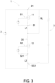
- FIG. 3 is a schematic circuit diagram illustrating a power module according to a first embodiment of the present disclosure.
- the power module 1 includes a first electrode terminal, a second electrode terminal, a first switch element 11, a second switch element 12, a first Kelvin source pin S2-1, and a second Kelvin source pin S2-2.
- the first and second electrode terminals are adapted to electrically connect to a power source 2, wherein the first and second electrode terminals of the power module 1 are configured to electrically connect to different terminals of the power source 2 respectively.
- the first and second electrode terminals of the power module 1 are electrically connected to a positive terminal and a negative terminal of the power source 2 respectively.
- the first switch element 11 is electrically connected between the first electrode terminal and the second switch element 12.
- the second switch element 12 is electrically connected between the first switch element 11 and the second electrode terminal and includes a source, a gate, and a drain, and the drain and the source of the second switch element 12 are electrically connected to the first switch element 11 and the second electrode terminal respectively.
- the first Kelvin source pin S2-1 is electrically connected to the source of the second switch element 12 and is adapted to receive a gate drive signal configured for driving the second switch element 12.
- the second Kelvin source pin S2-2 is electrically connected to the source of the second switch element 12 and is configured to be electrically connected to a snubber circuit 3.
- the snubber circuit 3 includes an inductor, a capacitor, and a resistor serially connected between the positive terminal of the power source 2 and the second Kelvin source pin S2-2, but not limited thereto.
- the snubber circuit 3 is adapted to absorb power loop ringing.
- RL is an inductor load, and all the inductors are parasitic inductors.
- the parasitic inductor may be replaced by a real inductor.
- first and second Kelvin source pins S2-1 and S2-2 of the power module 1 are dedicated for gate drive purpose and snubber design respectively. Therefore, the gate drive signal transmitted through the first Kelvin source pin S2-1 and the power transmitted through the second Kelvin source pin S2-2 may be decoupled with each other in some embodiments. In the embodiment, the gate drive signal transmitted through the first Kelvin source pin S2-1 and the power transmitted through the second Kelvin source pin S2-2 are decoupled with each other, thereby preventing the power loop ringing from polluting the gate drive signal.
- the power loop ringing is suppressed by the snubber circuit, the noise on gate drive loop is reduced due to the decoupling realized by the first and second Kelvin source pins S2-1 and S2-2, and thus the reliability of the power module 1 is enhanced.
- the power module 1 may include many switch elements connected in parallel, and the actual number of switch elements is determined according to actual requirements.
- the first switch element 11 and the second switch element 12 may be power semiconductor devices which may include but not limited to a diode or a field-effect transistor, such as MOSFET or IGBT (insulated gate bipolar transistor).
- the first switch element 11 may include a diode or a field-effect transistor, such as MOSFET or IGBT (insulated gate bipolar transistor)
- the second switch element 12 may include a field-effect transistor like MOSFET or IGBT.
- FIG. 4A is a schematic perspective view illustrating a packaging implementation of the power module according to the first embodiment of the present disclosure
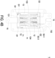
- FIG. 4B is a top view of the packaging implementation of the power module of FIG. 4A
- the first and second switch elements 11 and 12 are IGBTs.
- the power module 1 includes a plurality of first switch elements 11 connected in parallel and a plurality of second switch elements 12 connected in parallel.
- the power module 1 further includes a circuit board 13, a first source pin S1, a first gate pin G1, a first drain pin D1, a second gate pin G2, and a second drain pin D2.
- All of the first and second switch elements 11 and 12, the first source pin S1, the first gate pin G1, the first drain pin D1, the first and second Kelvin source pins S2-1 and S2-2, the second gate pin G2, and the second drain pin D2 are all disposed on the circuit board 13.
- the first source pin S1, the first gate pin G1, and the first drain pin D1 are electrically connected to sources, gates, and drains of the plurality of first switch elements 11 respectively.
- the first and second Kelvin source pins S2-1 and S2-2 are electrically connected to sources of the plurality of second switch elements 12 respectively.
- the second gate pin G2 and the second drain pin D2 are electrically connected to gates and drains of the plurality of second switch elements 12 respectively.
- Each pin is electrically connected to corresponding source, gate or drain of switch element through bonding wire, clip or conductive pattern on the circuit board 13.
- first Kelvin source pin S2-1 and the second Kelvin source pin S2-2 are electrically connected to the source of second switch elements 12 through different wire, clip or conductive pattern, so as to avoid interference and realize decoupling.
- the gate drive loop doesn't share the same source inductance (i.e., the inductance L2 shown in FIG. 3 ) with the snubber loop.
- the circuit board 13 is rectangular and has a first side 131, a second side 132, a third side 133, and a fourth side 134.
- the first side 131 is opposite to the second side 132
- the third side 133 is opposite to the fourth side 134.
- the first source pin S1, the first gate pin G1, the first drain pin D1, and the plurality of first switch elements 11 are disposed neighboring to the first side 131.
- the first and second Kelvin source pins S2-1 and S2-2, the second gate pin G2, the second drain pin D2, and the plurality of second switch elements 12 are disposed neighboring to the second side 132.
- the power module 1 includes the electrode terminals 14 and 15 adapted to be electrically connected to a power source for receiving power and outputting power.
- the power module 1 further includes pins T1 and T2 configured to be connected to thermistor.
- FIG. 5A is a schematic perspective view illustrating another packaging implementation of the power module according to the first embodiment of the present disclosure
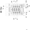
- FIG. 5B is a top view of the packaging implementation of the power module of FIG. 5A
- the first and second switch elements 11 and 12 are MOSFETs.
- the component parts and elements corresponding to those of FIG. 4A and FIG. 4B are designated by identical numeral references, and detailed descriptions thereof are omitted herein.
- the disposed positions of pins and switch elements in FIG. 5A and FIG. 5B are different.
- all the pins of the power module 1 are disposed neighboring to the second side 132, the plurality of first switch elements 11 are disposed along a central line between the third side 133 and the fourth side 134, and the plurality of second switch elements 12 are disposed between the plurality of first switch elements 11 and the third and fourth sides 133 and 134.
- the plurality of the second switch elements 12 are disposed on the region between the first switch elements 11 and the third side 133 and the region between the first switch elements 11 and the fourth side 134.
- the distance between the first and second Kelvin source pins S2-1 and S2-2 is the longest.
- the first switch element 11 shown in FIGS. 4A to 5B is implemented by IGBT or MOSFET, but not limited thereto.
- the first switch element 11 may be implemented by other types of transistors, such as junction gate field-effect transistor or bipolar junction transistor. In some embodiments, the first switch element 11 may be implemented by diode.
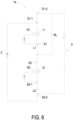
- FIG. 6 is a schematic circuit diagram illustrating a power module according to a second embodiment of the present disclosure, the component parts and elements corresponding to those of FIG. 3 are designated by identical numeral references, and detailed descriptions thereof are omitted herein.
- the first and second switch elements 11 and 12 are both field-effect transistors.
- the power module 1a according to the second embodiment further includes a first Kelvin collector pin D1-1 and a second Kelvin collector pin D1-2.
- the drain and source of the first switch element 11 are electrically connected to the power source 2 and the drain of the second switch element 12 respectively.
- the first and second Kelvin collector pins D1-1 and D1-2 are electrically connected to the drain of the first switch element 11 respectively.
- the first Kelvin collector pin D1-1 is configured to be electrically connected to a detection circuit (not shown) for desaturation protection.
- the detection circuit is adapted to protect the first switch element 11 from short circuit fault.
- the second Kelvin collector pin D1-2 is configured to be electrically connected to the snubber circuit 3. The detecting signal transmitted through the first Kelvin collector pin D1-1 for desaturation sensing and the power transmitted through the second Kelvin collector pin D1-2 are decoupled with each other.
- the power module 1a may include many switch elements connected in parallel for increasing the output current, and the actual number of switch elements is determined according to actual requirements.
- Two packaging implementations of the power module 1a are exemplified as follows.
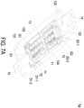
- FIG. 7A is a schematic perspective view illustrating a packaging implementation of the power module according to the second embodiment of the present disclosure
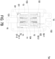
- FIG. 7B is a top view of the packaging implementation of the power module of FIG. 7A
- the component parts and elements corresponding to those of FIG. 4A and FIG. 4B are designated by identical numeral references, and detailed descriptions thereof are omitted herein.
- the first and second switch elements 11 and 12 are IGBTs.
- the first and second Kelvin collector pins D1-1 and D1-2 are disposed on the circuit board 13 and are neighboring to the first side 131.
- the first and second Kelvin collector pins D1-1 and D1-2 are electrically connected to drains of the plurality of first switch elements 11 respectively through bonding wire or conductive pattern on the circuit board 13.
- FIG. 8A is a schematic perspective view illustrating another packaging implementation of the power module according to the second embodiment of the present disclosure
- FIG. 8B is a top view of the packaging implementation of the power module of FIG. 8A
- the component parts and elements corresponding to those of FIG. 5A and FIG. 5B are designated by identical numeral references, and detailed descriptions thereof are omitted herein.
- the first and second switch elements 11 and 12 are MOSFETs.
- the first and second Kelvin collector pins D1-1 and D1-2 are disposed on the circuit board 13 and are neighboring to the second side 132.
- the first and second Kelvin collector pins D1-1 and D1-2 are electrically connected to drains of the plurality of first switch elements 11 respectively through bonding wire or conductive pattern on the circuit board 13.
- the present disclosure provides a power module capable of decoupling the power loop and the gate drive loop by utilizing Kelvin pins.
- the power module includes two Kelvin pins dedicated for gate drive purpose and snubber design respectively. Therefore, the power loop ringing is prevented from polluting the gate drive signal. Consequently, the power loop ringing is suppressed, the noise on gate drive loop is reduced, and the reliability of the power module is enhanced.
Landscapes
- Engineering & Computer Science (AREA)
- Power Engineering (AREA)
- Physics & Mathematics (AREA)
- Electromagnetism (AREA)
- Power Conversion In General (AREA)
- Electronic Switches (AREA)
- Inverter Devices (AREA)
- Direct Current Feeding And Distribution (AREA)
- Geometry (AREA)
Abstract
Description
- The present disclosure relates to a power module, and more particularly to a power module capable of decoupling the power loop and the gate drive loop by utilizing Kelvin pins.
- SiC power module becomes a new hot topic in automotive traction inverter applications. Despite significant improvements in switching loss, the switching ringing as depicted in
FIG. 1 may lead to EMC (electromagnetic compatibility) test failures. InFIG. 1 , the three waveforms represent low-side MOSFET (metal-oxide-semiconductor field-effect transistor) turn on transient. Vds H is the diode voltage of the high-side MOSFET, Ids H is the freewheeling current through the high-side MOSFET, and Vge terminal is gate signal of the low-side MOSFET being turned on. As shown inFIG. 1 , when the low-side MOSFET turns on, switching ringing is observed on high-side diode switching waveform. Conventionally, introducing a snubber circuit to the system is a common practice to suppress voltage spike and ringing. - On the other hand, in order to fulfill the increasing demand for greater output current in inverter application, power module now has many dies connected in parallel. However, most of the power module has no dedicated pins for snubber design. Consequently, the snubber circuit added to the circuit needs to be directly connected to the source and drain signal pins of switch. The snubber and gate drive loops then share part of parasitic in power module. This particular type of connection may couple power loop noise into the gate driver loop and lead to gate oscillation issue. As shown in
FIG. 2 , due to snubber implementation, noise from snubber circuit causes big voltage spike in gate signal. The low side MOSFET gate oscillation may lead to gate failure and reduce power module reliability. - Therefore, there is a need of providing a power module to obviate the drawbacks encountered from the prior arts.
- It is an objective of the present disclosure to provide a power module capable of decoupling the power loop and the gate drive loop by utilizing Kelvin pins. In particular, the power module includes two Kelvin pins dedicated for gate drive purpose and snubber design respectively. Therefore, the power loop ringing is prevented from polluting the gate drive signal. Consequently, the power loop ringing is suppressed, the noise on gate drive loop is reduced, and the reliability of the power module is enhanced.
- In accordance with an aspect of the present disclosure, there is provided a power module including a first electrode terminal, a second electrode terminal, a first switch element, a second switch element, a first Kelvin source pin, and a second Kelvin source pin. The first switch element is electrically connected to the first electrode terminal. The second switch element is electrically connected between the first switch element and the second electrode terminal and includes a drain and a source electrically connected to the first switch element and the second electrode terminal respectively. The first Kelvin source pin is electrically connected to the source of the second switch element and is adapted to receive a gate drive signal for driving the second switch element. The second Kelvin source pin is electrically connected to the source of the second switch element and is configured to be electrically connected to a snubber circuit.
-
-
FIGS. 1 and2 are schematic oscillograms showing waveforms of the diode voltage and current of the high-side MOSFET and the gate signal of the low-side MOSFET during turn on transient of the low-side MOSFET; -
FIG. 3 is a schematic circuit diagram illustrating a power module according to a first embodiment of the present disclosure; -
FIG. 4A is a schematic perspective view illustrating a packaging implementation of the power module according to the first embodiment of the present disclosure; -
FIG. 4B is a top view of the packaging implementation of the power module ofFIG. 4A ; -
FIG. 5A is a schematic perspective view illustrating another packaging implementation of the power module according to the first embodiment of the present disclosure; -
FIG. 5B is a top view of the packaging implementation of the power module ofFIG. 5 ; -
FIG. 6 is a schematic circuit diagram illustrating a power module according to a second embodiment of the present disclosure; -
FIG. 7A is a schematic perspective view illustrating a packaging implementation of the power module according to the second embodiment of the present disclosure; -
FIG. 7B is a top view of the packaging implementation of the power module ofFIG. 7A ; -
FIG. 8A is a schematic perspective view illustrating another packaging implementation of the power module according to the second embodiment of the present disclosure; and -
FIG. 8B is a top view of the packaging implementation of the power module ofFIG. 8A . - The present disclosure will now be described more specifically with reference to the following embodiments. It is to be noted that the following descriptions of preferred embodiments of this disclosure are presented herein for purpose of illustration and description only. It is not intended to be exhaustive or to be limited to the precise form disclosed.
- The present invention will now be described more specifically with reference to the following embodiments. It is to be noted that the following descriptions of preferred embodiments of this invention are presented herein for purpose of illustration and description only; it is not intended to be exhaustive or to be limited to the precise form disclosed. For example, the formation of a first feature over or on a second feature in the description that follows may include embodiments in which the first and second features are formed in direct contact, and may also include embodiments in which additional features may be formed between the first and second features, such that the first and second features may not be in direct contact. In addition, the present disclosure may repeat reference numerals and/or letters in the various examples. This repetition is for the purpose of simplicity and clarity and does not in itself dictate a relationship between the various embodiments and/or configurations discussed. Further, spatially relative terms, such as "beneath," "below," "lower," "above," "upper" and the like, may be used herein for ease of description to describe one element or feature's relationship to another element(s) or feature(s) as illustrated in the figures. The spatially relative terms are intended to encompass different orientations of the device in use or operation in addition to the orientation depicted in the figures. The apparatus may be otherwise oriented (rotated 90 degrees or at other orientations) and the spatially relative descriptors used herein may likewise be interpreted accordingly. When an element is referred to as being "connected," or "coupled," to another element, it can be directly connected or coupled to the other element or intervening elements may be present. Although the wide numerical ranges and parameters of the present disclosure are approximations, numerical values are set forth in the specific examples as precisely as possible. In addition, although the "first," "second," "third," and the like terms in the claims be used to describe the various elements can be appreciated, these elements should not be limited by these terms, and these elements are described in the respective embodiments are used to express the different reference numerals, these terms are only used to distinguish one element from another element. For example, a first element could be termed a second element, and, similarly, a second element could be termed a first element, without departing from the scope of example embodiments. Besides, "and / or" and the like may be used herein for including any or all combinations of one or more of the associated listed items. While the numerical ranges and parameters set forth for the broad scope of the present invention are approximations, the numerical value reported in the specific examples set forth as accurately as possible. However, any numerical values inherently contain certain errors necessarily the standard deviation found in the respective testing measurements caused. Also, as used herein, the term "about" generally means away from a given value or a range of 10%, 5%, 1% or 0.5%. Alternatively, the word "about" means within an acceptable standard error of ordinary skill in the art-recognized average. In addition to the operation / working examples, or unless otherwise specifically stated otherwise, in all cases, all of the numerical ranges, amounts, values and percentages, such as the number for the herein disclosed materials, time duration, temperature, operating conditions, the ratio of the amount, and the like, should be understood as the word "about" decorator. Accordingly, unless otherwise indicated, the numerical parameters of the present invention and scope of the appended patent proposed is to follow changes in the desired approximations. At least, the number of significant digits for each numerical parameter should at least be reported and explained by conventional rounding technique is applied. Herein, it can be expressed as a range between from one endpoint to the other or both endpoints. Unless otherwise specified, all ranges disclosed herein are inclusive.
-
FIG. 3 is a schematic circuit diagram illustrating a power module according to a first embodiment of the present disclosure. As shown inFIG. 3 , thepower module 1 includes a first electrode terminal, a second electrode terminal, afirst switch element 11, asecond switch element 12, a first Kelvin source pin S2-1, and a second Kelvin source pin S2-2. The first and second electrode terminals are adapted to electrically connect to apower source 2, wherein the first and second electrode terminals of thepower module 1 are configured to electrically connect to different terminals of thepower source 2 respectively. In the embodiment, the first and second electrode terminals of thepower module 1 are electrically connected to a positive terminal and a negative terminal of thepower source 2 respectively. Thefirst switch element 11 is electrically connected between the first electrode terminal and thesecond switch element 12. Thesecond switch element 12 is electrically connected between thefirst switch element 11 and the second electrode terminal and includes a source, a gate, and a drain, and the drain and the source of thesecond switch element 12 are electrically connected to thefirst switch element 11 and the second electrode terminal respectively. The first Kelvin source pin S2-1 is electrically connected to the source of thesecond switch element 12 and is adapted to receive a gate drive signal configured for driving thesecond switch element 12. The second Kelvin source pin S2-2 is electrically connected to the source of thesecond switch element 12 and is configured to be electrically connected to asnubber circuit 3. As an example, thesnubber circuit 3 includes an inductor, a capacitor, and a resistor serially connected between the positive terminal of thepower source 2 and the second Kelvin source pin S2-2, but not limited thereto. In one embodiment, thesnubber circuit 3 is adapted to absorb power loop ringing. In one embodiment, RL is an inductor load, and all the inductors are parasitic inductors. In an embodiment, the parasitic inductor may be replaced by a real inductor. - It is noted that the first and second Kelvin source pins S2-1 and S2-2 of the
power module 1 are dedicated for gate drive purpose and snubber design respectively. Therefore, the gate drive signal transmitted through the first Kelvin source pin S2-1 and the power transmitted through the second Kelvin source pin S2-2 may be decoupled with each other in some embodiments. In the embodiment, the gate drive signal transmitted through the first Kelvin source pin S2-1 and the power transmitted through the second Kelvin source pin S2-2 are decoupled with each other, thereby preventing the power loop ringing from polluting the gate drive signal. Consequently, the power loop ringing is suppressed by the snubber circuit, the noise on gate drive loop is reduced due to the decoupling realized by the first and second Kelvin source pins S2-1 and S2-2, and thus the reliability of thepower module 1 is enhanced. - For increasing the output current, the
power module 1 may include many switch elements connected in parallel, and the actual number of switch elements is determined according to actual requirements. In some embodiments, thefirst switch element 11 and thesecond switch element 12 may be power semiconductor devices which may include but not limited to a diode or a field-effect transistor, such as MOSFET or IGBT (insulated gate bipolar transistor). In one embodiment, thefirst switch element 11 may include a diode or a field-effect transistor, such as MOSFET or IGBT (insulated gate bipolar transistor), and thesecond switch element 12 may include a field-effect transistor like MOSFET or IGBT. Two packaging implementations of thepower module 1 are exemplified as follows. -
FIG. 4A is a schematic perspective view illustrating a packaging implementation of the power module according to the first embodiment of the present disclosure, andFIG. 4B is a top view of the packaging implementation of the power module ofFIG. 4A . In the packaging implementation ofFIG. 4A andFIG. 4B , the first andsecond switch elements FIG. 4A andFIG. 4B , thepower module 1 includes a plurality offirst switch elements 11 connected in parallel and a plurality ofsecond switch elements 12 connected in parallel. Moreover, thepower module 1 further includes acircuit board 13, a first source pin S1, a first gate pin G1, a first drain pin D1, a second gate pin G2, and a second drain pin D2. All of the first andsecond switch elements circuit board 13. The first source pin S1, the first gate pin G1, and the first drain pin D1 are electrically connected to sources, gates, and drains of the plurality offirst switch elements 11 respectively. The first and second Kelvin source pins S2-1 and S2-2 are electrically connected to sources of the plurality ofsecond switch elements 12 respectively. The second gate pin G2 and the second drain pin D2 are electrically connected to gates and drains of the plurality ofsecond switch elements 12 respectively. The relations of electrical connection among the pins and switch elements are shown inFIG. 3 as well. Each pin is electrically connected to corresponding source, gate or drain of switch element through bonding wire, clip or conductive pattern on thecircuit board 13. It is noted that the first Kelvin source pin S2-1 and the second Kelvin source pin S2-2 are electrically connected to the source ofsecond switch elements 12 through different wire, clip or conductive pattern, so as to avoid interference and realize decoupling. Further, since the first and second Kelvin source pins S2-1 and S2-2 are laid out separately, the gate drive loop doesn't share the same source inductance (i.e., the inductance L2 shown inFIG. 3 ) with the snubber loop. - The
circuit board 13 is rectangular and has afirst side 131, asecond side 132, athird side 133, and afourth side 134. Thefirst side 131 is opposite to thesecond side 132, and thethird side 133 is opposite to thefourth side 134. The first source pin S1, the first gate pin G1, the first drain pin D1, and the plurality offirst switch elements 11 are disposed neighboring to thefirst side 131. The first and second Kelvin source pins S2-1 and S2-2, the second gate pin G2, the second drain pin D2, and the plurality ofsecond switch elements 12 are disposed neighboring to thesecond side 132. In addition, thepower module 1 includes theelectrode terminals power module 1 further includes pins T1 and T2 configured to be connected to thermistor. -
FIG. 5A is a schematic perspective view illustrating another packaging implementation of the power module according to the first embodiment of the present disclosure, andFIG. 5B is a top view of the packaging implementation of the power module ofFIG. 5A . In the packaging implementation ofFIG. 5A andFIG. 5B , the first andsecond switch elements FIG. 5A andFIG. 5B , the component parts and elements corresponding to those ofFIG. 4A andFIG. 4B are designated by identical numeral references, and detailed descriptions thereof are omitted herein. Compared withFIG. 4A andFIG. 4B , the disposed positions of pins and switch elements inFIG. 5A andFIG. 5B are different. In particular, as shown inFIG. 5A andFIG. 5B , all the pins of thepower module 1 are disposed neighboring to thesecond side 132, the plurality offirst switch elements 11 are disposed along a central line between thethird side 133 and thefourth side 134, and the plurality ofsecond switch elements 12 are disposed between the plurality offirst switch elements 11 and the third andfourth sides second switch elements 12 are disposed on the region between thefirst switch elements 11 and thethird side 133 and the region between thefirst switch elements 11 and thefourth side 134. In an embodiment, in all the pins electrically connected to thesecond switch elements 12, the distance between the first and second Kelvin source pins S2-1 and S2-2 is the longest. - In addition, the
first switch element 11 shown inFIGS. 4A to 5B is implemented by IGBT or MOSFET, but not limited thereto. Thefirst switch element 11 may be implemented by other types of transistors, such as junction gate field-effect transistor or bipolar junction transistor. In some embodiments, thefirst switch element 11 may be implemented by diode. -
FIG. 6 is a schematic circuit diagram illustrating a power module according to a second embodiment of the present disclosure, the component parts and elements corresponding to those ofFIG. 3 are designated by identical numeral references, and detailed descriptions thereof are omitted herein. In the second embodiment, the first andsecond switch elements FIG. 6 , thepower module 1a according to the second embodiment further includes a first Kelvin collector pin D1-1 and a second Kelvin collector pin D1-2. The drain and source of thefirst switch element 11 are electrically connected to thepower source 2 and the drain of thesecond switch element 12 respectively. The first and second Kelvin collector pins D1-1 and D1-2 are electrically connected to the drain of thefirst switch element 11 respectively. The first Kelvin collector pin D1-1 is configured to be electrically connected to a detection circuit (not shown) for desaturation protection. In specific, the detection circuit is adapted to protect thefirst switch element 11 from short circuit fault. With the first Kelvin collector pin D1-1, the power loop is separated from the desaturation sensing path, and thus the switching ringing on thefirst switch element 11 is prevented from affecting the desaturation sensitivity during transient. The second Kelvin collector pin D1-2 is configured to be electrically connected to thesnubber circuit 3. The detecting signal transmitted through the first Kelvin collector pin D1-1 for desaturation sensing and the power transmitted through the second Kelvin collector pin D1-2 are decoupled with each other. - Similar to the
power module 1 of the first embodiment, thepower module 1a may include many switch elements connected in parallel for increasing the output current, and the actual number of switch elements is determined according to actual requirements. Two packaging implementations of thepower module 1a are exemplified as follows. -
FIG. 7A is a schematic perspective view illustrating a packaging implementation of the power module according to the second embodiment of the present disclosure,FIG. 7B is a top view of the packaging implementation of the power module ofFIG. 7A . InFIG. 7A andFIG. 7B , the component parts and elements corresponding to those ofFIG. 4A andFIG. 4B are designated by identical numeral references, and detailed descriptions thereof are omitted herein. Further, inFIG. 7A andFIG. 7B , the first andsecond switch elements FIG. 7A andFIG. 7B , the first and second Kelvin collector pins D1-1 and D1-2 are disposed on thecircuit board 13 and are neighboring to thefirst side 131. The first and second Kelvin collector pins D1-1 and D1-2 are electrically connected to drains of the plurality offirst switch elements 11 respectively through bonding wire or conductive pattern on thecircuit board 13. -
FIG. 8A is a schematic perspective view illustrating another packaging implementation of the power module according to the second embodiment of the present disclosure,FIG. 8B is a top view of the packaging implementation of the power module ofFIG. 8A . InFIG. 8A andFIG. 8B , the component parts and elements corresponding to those ofFIG. 5A andFIG. 5B are designated by identical numeral references, and detailed descriptions thereof are omitted herein. Further, inFIG. 8A andFIG. 8B , the first andsecond switch elements FIG. 8A andFIG. 8B , the first and second Kelvin collector pins D1-1 and D1-2 are disposed on thecircuit board 13 and are neighboring to thesecond side 132. The first and second Kelvin collector pins D1-1 and D1-2 are electrically connected to drains of the plurality offirst switch elements 11 respectively through bonding wire or conductive pattern on thecircuit board 13. - From the above descriptions, the present disclosure provides a power module capable of decoupling the power loop and the gate drive loop by utilizing Kelvin pins. In particular, the power module includes two Kelvin pins dedicated for gate drive purpose and snubber design respectively. Therefore, the power loop ringing is prevented from polluting the gate drive signal. Consequently, the power loop ringing is suppressed, the noise on gate drive loop is reduced, and the reliability of the power module is enhanced.
Claims (12)
- A power module (1), characterized by comprising:a first electrode terminal and a second electrode terminal adapted to electrically connect to a power source (2);a first switch element (11) electrically connected to the first electrode terminal;a second switch element (12) electrically connected between the first switch element (11) and the second electrode terminal and comprising a drain and a source electrically connected to the first switch element (11) and the second electrode terminal respectively;a first Kelvin source pin (S2-1) electrically connected to the source of the second switch element (12) and adapted to receive a gate drive signal for driving the second switch element (12); anda second Kelvin source pin (S2-2) electrically connected to the source of the second switch element (12) and configured to be electrically connected to a snubber circuit (3).
- The power module according to claim 1, wherein the gate drive signal transmitted through the first Kelvin source pin (S2-1) and a power transmitted through the second Kelvin source pin (S2-2) are decoupled with each other.
- The power module according to claim 1, further comprising a circuit board (13), a first source pin (S1), a first gate pin (G1), a first drain pin (D1), a second gate pin (G2), and a second drain pin (D2), wherein the power module (1) comprises a plurality of said first switch elements (11) and a plurality of said second switch elements (12), all the switch elements and pins of the power module (1) are disposed on the circuit board (13), the first source pin (SI), the first gate pin (G1), and the first drain pin (D1) are electrically connected to sources, gates, and drains of the plurality of first switch elements (11) respectively, the second gate pin (G2) and the second drain pin (D2) are electrically connected to gates and drains of the plurality of second switch elements (12) respectively, and the first and second Kelvin source pins (S2-1, S2-2) are electrically connected to sources of the plurality of second switch elements (12) respectively.
- The power module according to claim 3, wherein the circuit board (13) has a first side (131) and a second side (132) opposite to the first side (131), the first source pin (S1), the first gate pin (G1), the first drain pin (D1), and the plurality of first switch elements (11) are disposed neighboring to the first side (131), and the first Kelvin source pin (S2-1), the second Kelvin source pin (S2-2), the second gate pin (G2), the second drain pin (D2), and the plurality of second switch elements (12) are disposed neighboring to the second side (132).
- The power module according to claim 3, wherein the circuit board (13) has a first side (131), a second side (132), a third side (133), and a fourth side (134), the first side (131) is opposite to the second side (132), the third side (133) is opposite to the fourth side (134), all the pins of the power module (1) are disposed neighboring to the second side (132), the plurality of first switch elements (11) are disposed along a central line between the third and fourth sides (133, 134), and the plurality of second switch elements (12) are disposed between the plurality of first switch elements (11) and the third and fourth sides (133, 134).
- The power module according to claim 1, wherein the first switch element (11) comprises a diode, and the second switch element (12) comprises a field-effect transistor.
- The power module according to claim 1, wherein the first and second switch elements (11, 12) comprise field-effect transistors.
- The power module according to claim 7, wherein the first switch element (11) comprises a drain and a source electrically connected to the first electrode terminal and the drain of the second switch element (12) respectively, the power module (1a) further comprises a first Kelvin collector pin (D1-1) and a second Kelvin collector pin (D1-2) electrically connected to the drain of the first switch element (11) respectively, the first Kelvin collector pin (D1-1) is configured to be electrically connected to a detection circuit for desaturation protection, and the second Kelvin collector pin (D1-2) is configured to be electrically connected to the snubber circuit (3).
- The power module according to claim 8, wherein a detecting signal transmitted through the first Kelvin collector pin (D1-1) and a power transmitted through the second Kelvin collector pin (D1-2) are decoupled with each other.
- The power module according to claim 8, further comprising a circuit board (13), a first source pin (SI), a first gate pin (G1), a second gate pin (G2), and a second drain pin (D2), wherein the power module (1a) comprises a plurality of said first switch elements (11) and a plurality of said second switch elements (12), the switch elements and pins of the power module (1a) are disposed on the circuit board (13); the first source pin (SI) and the first gate pin (G1) are electrically connected to sources and gates of the plurality of first switch elements (11) respectively, the first and second Kelvin collector pins (D1-1, D1-2) are electrically connected to drains of the plurality of first switch elements (11), the second gate pin (G2) and the second drain pin (D2) are electrically connected to gates and drains of the plurality of second switch elements (12) respectively, and the first and second Kelvin source pins (S2-1, S2-2) are electrically connected to sources of the plurality of second switch elements (12).
- The power module according to claim 10, wherein the circuit board (13) has a first side (131) and a second side (132) opposite to the first side (131), the first source pin (SI), the first gate pin (G1), the first and second Kelvin collector pins (D1-1, D1-2), and the plurality of first switch elements (11) are disposed neighboring to the first side (131), and the first and second Kelvin source pins (S2-1, S2-2), the second gate pin (G2), the second drain pin (D2), and the plurality of second switch elements (12) are disposed neighboring to the second side (132).
- The power module according to claim 10, wherein the circuit board (13) has a first side (131), a second side (132), a third side (133), and a fourth side (134), the first side (131) is opposite to the second side (132), the third side (133) is opposite to the fourth side (134), all the pins of the power module (1a) are disposed neighboring to the second side (132), the plurality of first switch elements (11) are disposed along a central line between the third and fourth sides (133, 134), and the plurality of second switch elements (12) are disposed between the plurality of first switch elements (11) and the third and fourth sides (133, 134).
Applications Claiming Priority (1)
| Application Number | Priority Date | Filing Date | Title |
|---|---|---|---|
| US17/541,543 US12375006B2 (en) | 2021-12-03 | 2021-12-03 | Power module |
Publications (2)
| Publication Number | Publication Date |
|---|---|
| EP4191645A2 true EP4191645A2 (en) | 2023-06-07 |
| EP4191645A3 EP4191645A3 (en) | 2023-06-14 |
Family
ID=84358662
Family Applications (1)
| Application Number | Title | Priority Date | Filing Date |
|---|---|---|---|
| EP22208026.9A Pending EP4191645A3 (en) | 2021-12-03 | 2022-11-17 | Power module |
Country Status (4)
| Country | Link |
|---|---|
| US (1) | US12375006B2 (en) |
| EP (1) | EP4191645A3 (en) |
| JP (1) | JP7564177B2 (en) |
| CN (1) | CN116232026A (en) |
Families Citing this family (1)
| Publication number | Priority date | Publication date | Assignee | Title |
|---|---|---|---|---|
| US11936368B2 (en) * | 2022-06-26 | 2024-03-19 | Wolfspeed, Inc. | Optimization of power module performance via parasitic mutual coupling |
Family Cites Families (22)
| Publication number | Priority date | Publication date | Assignee | Title |
|---|---|---|---|---|
| US5170337A (en) | 1992-01-29 | 1992-12-08 | General Electric Company | Low-inductance package for multiple paralleled devices operating at high frequency |
| US6703703B2 (en) | 2000-01-12 | 2004-03-09 | International Rectifier Corporation | Low cost power semiconductor module without substrate |
| US7551007B2 (en) * | 2005-02-11 | 2009-06-23 | Fairchild Semiconductor Corporation | Partial switch gate driver |
| JP5099243B2 (en) | 2010-04-14 | 2012-12-19 | 株式会社デンソー | Semiconductor module |
| US9640617B2 (en) | 2011-09-11 | 2017-05-02 | Cree, Inc. | High performance power module |
| JP2013165578A (en) | 2012-02-10 | 2013-08-22 | Sinfonia Technology Co Ltd | Gate drive circuit of self arc-extinguishing type semiconductor element and power conversion apparatus |
| KR102153041B1 (en) | 2013-12-04 | 2020-09-07 | 삼성전자주식회사 | Semiconductor device package and method of manufacturing the same |
| JP6425380B2 (en) * | 2013-12-26 | 2018-11-21 | ローム株式会社 | Power circuit and power module |
| JP6683621B2 (en) * | 2014-10-30 | 2020-04-22 | ローム株式会社 | Power modules and power circuits |
| JP6869183B2 (en) | 2015-02-17 | 2021-05-12 | コーニンクレッカ フィリップス エヌ ヴェKoninklijke Philips N.V. | Ceramic substrate and method for manufacturing ceramic substrate |
| CN205104489U (en) | 2015-11-23 | 2016-03-23 | 南京晟芯半导体有限公司 | Insulating section mould piece packaging structure |
| US9994110B2 (en) | 2016-08-30 | 2018-06-12 | Ford Global Technologies, Llc | Dual gate solid state devices to reduce switching loss |
| US10749443B2 (en) * | 2017-01-13 | 2020-08-18 | Cree Fayetteville, Inc. | High power multilayer module having low inductance and fast switching for paralleling power devices |
| GB2564700A (en) | 2017-07-21 | 2019-01-23 | Rolls Royce Plc | A power electronics module and a method of detecting a fault in a power electronics module |
| JP7097742B2 (en) * | 2018-05-01 | 2022-07-08 | ルネサスエレクトロニクス株式会社 | Semiconductor devices and their manufacturing methods |
| JP7224918B2 (en) * | 2019-01-04 | 2023-02-20 | 株式会社東芝 | Semiconductor devices and semiconductor packages |
| US10700681B1 (en) | 2019-03-15 | 2020-06-30 | Ford Global Technologies, Llc | Paralleled power module with additional emitter/source path |
| JP2021005690A (en) | 2019-06-27 | 2021-01-14 | 住友電気工業株式会社 | Semiconductor module |
| JP7142784B2 (en) | 2019-07-24 | 2022-09-27 | 日立Astemo株式会社 | electric circuit device |
| CN112768427B (en) | 2019-11-05 | 2024-09-17 | 英诺赛科(珠海)科技有限公司 | Packaging structure and packaging method of GaN HEMT |
| WO2021130290A1 (en) | 2019-12-28 | 2021-07-01 | Danfoss Silicon Power Gmbh | Power module with improved electrical characteristics |
| CN113345852B (en) * | 2021-05-26 | 2025-03-21 | 全球能源互联网研究院有限公司 | A compression type power chip packaging structure |
-
2021
- 2021-12-03 US US17/541,543 patent/US12375006B2/en active Active
-
2022
- 2022-11-17 JP JP2022184262A patent/JP7564177B2/en active Active
- 2022-11-17 EP EP22208026.9A patent/EP4191645A3/en active Pending
- 2022-12-01 CN CN202211537646.4A patent/CN116232026A/en active Pending
Also Published As
| Publication number | Publication date |
|---|---|
| CN116232026A (en) | 2023-06-06 |
| US20230178490A1 (en) | 2023-06-08 |
| EP4191645A3 (en) | 2023-06-14 |
| US12375006B2 (en) | 2025-07-29 |
| JP7564177B2 (en) | 2024-10-08 |
| JP2023083224A (en) | 2023-06-15 |
Similar Documents
| Publication | Publication Date | Title |
|---|---|---|
| US10607978B2 (en) | Semiconductor device and electronic apparatus | |
| JP6425380B2 (en) | Power circuit and power module | |
| JP6130863B2 (en) | Semiconductor power module and device | |
| KR101571952B1 (en) | Switching circuit and semiconductor module | |
| US11652399B2 (en) | Miller clamp protection circuit, driving circuit, driving chip and intelligent IGBT module | |
| US7560833B2 (en) | Drive circuit having a transformer for a semiconductor switching element | |
| CN114172123B (en) | Semiconductor device with a semiconductor device having a plurality of semiconductor chips | |
| CN108831880B (en) | A DBC substrate for MOS modules of power electronic devices | |
| US11515868B2 (en) | Electronic circuit and semiconductor module | |
| US20180182730A1 (en) | Common contact semiconductor device package | |
| US12375006B2 (en) | Power module | |
| US20180366567A1 (en) | Semiconductor device | |
| US10700681B1 (en) | Paralleled power module with additional emitter/source path | |
| CN109660114B (en) | Driving circuit of multipath parallel MOS (metal oxide semiconductor) tubes | |
| US10396774B2 (en) | Intelligent power module operable to be driven by negative gate voltage | |
| US20230421145A1 (en) | Optimization of power module performance via parasitic mutual coupling | |
| US12588570B2 (en) | Semiconductor device | |
| CN107395178B (en) | Semiconductor power switching device and electronic apparatus | |
| TW202543242A (en) | Asymmetric common source inductances to reduce turn-off overvoltage in mosfets | |
| Kapaun et al. | Switching performance of GaN-HEMT compared to Si-devices in new converters based on scalable converter cell structures | |
| WO2023145144A1 (en) | Power semiconductor module | |
| JP2018026962A (en) | Switching device |
Legal Events
| Date | Code | Title | Description |
|---|---|---|---|
| PUAI | Public reference made under article 153(3) epc to a published international application that has entered the european phase |
Free format text: ORIGINAL CODE: 0009012 |
|
| STAA | Information on the status of an ep patent application or granted ep patent |
Free format text: STATUS: THE APPLICATION HAS BEEN PUBLISHED |
|
| PUAL | Search report despatched |
Free format text: ORIGINAL CODE: 0009013 |
|
| AK | Designated contracting states |
Kind code of ref document: A2 Designated state(s): AL AT BE BG CH CY CZ DE DK EE ES FI FR GB GR HR HU IE IS IT LI LT LU LV MC ME MK MT NL NO PL PT RO RS SE SI SK SM TR |
|
| AK | Designated contracting states |
Kind code of ref document: A3 Designated state(s): AL AT BE BG CH CY CZ DE DK EE ES FI FR GB GR HR HU IE IS IT LI LT LU LV MC ME MK MT NL NO PL PT RO RS SE SI SK SM TR |
|
| RIC1 | Information provided on ipc code assigned before grant |
Ipc: H03K 17/082 20060101ALN20230509BHEP Ipc: H02M 1/08 20060101ALN20230509BHEP Ipc: H01L 23/00 20060101ALI20230509BHEP Ipc: H02M 7/00 20060101ALI20230509BHEP Ipc: H01L 23/498 20060101ALI20230509BHEP Ipc: H01L 25/07 20060101ALI20230509BHEP Ipc: H01L 21/60 20060101AFI20230509BHEP |
|
| STAA | Information on the status of an ep patent application or granted ep patent |
Free format text: STATUS: REQUEST FOR EXAMINATION WAS MADE |
|
| 17P | Request for examination filed |
Effective date: 20231214 |
|
| RBV | Designated contracting states (corrected) |
Designated state(s): AL AT BE BG CH CY CZ DE DK EE ES FI FR GB GR HR HU IE IS IT LI LT LU LV MC ME MK MT NL NO PL PT RO RS SE SI SK SM TR |