EP4191294A1 - Optical interference filter - Google Patents
Optical interference filter Download PDFInfo
- Publication number
- EP4191294A1 EP4191294A1 EP22210677.5A EP22210677A EP4191294A1 EP 4191294 A1 EP4191294 A1 EP 4191294A1 EP 22210677 A EP22210677 A EP 22210677A EP 4191294 A1 EP4191294 A1 EP 4191294A1
- Authority
- EP
- European Patent Office
- Prior art keywords
- layers
- subset
- interference filter
- optical interference
- refractive index
- Prior art date
- Legal status (The legal status is an assumption and is not a legal conclusion. Google has not performed a legal analysis and makes no representation as to the accuracy of the status listed.)
- Pending
Links
Images






Classifications
-
- C—CHEMISTRY; METALLURGY
- C23—COATING METALLIC MATERIAL; COATING MATERIAL WITH METALLIC MATERIAL; CHEMICAL SURFACE TREATMENT; DIFFUSION TREATMENT OF METALLIC MATERIAL; COATING BY VACUUM EVAPORATION, BY SPUTTERING, BY ION IMPLANTATION OR BY CHEMICAL VAPOUR DEPOSITION, IN GENERAL; INHIBITING CORROSION OF METALLIC MATERIAL OR INCRUSTATION IN GENERAL
- C23C—COATING METALLIC MATERIAL; COATING MATERIAL WITH METALLIC MATERIAL; SURFACE TREATMENT OF METALLIC MATERIAL BY DIFFUSION INTO THE SURFACE, BY CHEMICAL CONVERSION OR SUBSTITUTION; COATING BY VACUUM EVAPORATION, BY SPUTTERING, BY ION IMPLANTATION OR BY CHEMICAL VAPOUR DEPOSITION, IN GENERAL
- C23C14/00—Coating by vacuum evaporation, by sputtering or by ion implantation of the coating forming material
- C23C14/06—Coating by vacuum evaporation, by sputtering or by ion implantation of the coating forming material characterised by the coating material
- C23C14/0617—AIII BV compounds, where A is Al, Ga, In or Tl and B is N, P, As, Sb or Bi
-
- G—PHYSICS
- G02—OPTICS
- G02B—OPTICAL ELEMENTS, SYSTEMS OR APPARATUS
- G02B5/00—Optical elements other than lenses
- G02B5/20—Filters
- G02B5/28—Interference filters
- G02B5/285—Interference filters comprising deposited thin solid films
- G02B5/286—Interference filters comprising deposited thin solid films having four or fewer layers, e.g. for achieving a colour effect
-
- G—PHYSICS
- G02—OPTICS
- G02B—OPTICAL ELEMENTS, SYSTEMS OR APPARATUS
- G02B5/00—Optical elements other than lenses
- G02B5/20—Filters
- G02B5/28—Interference filters
- G02B5/285—Interference filters comprising deposited thin solid films
- G02B5/288—Interference filters comprising deposited thin solid films comprising at least one thin film resonant cavity, e.g. in bandpass filters
-
- C—CHEMISTRY; METALLURGY
- C23—COATING METALLIC MATERIAL; COATING MATERIAL WITH METALLIC MATERIAL; CHEMICAL SURFACE TREATMENT; DIFFUSION TREATMENT OF METALLIC MATERIAL; COATING BY VACUUM EVAPORATION, BY SPUTTERING, BY ION IMPLANTATION OR BY CHEMICAL VAPOUR DEPOSITION, IN GENERAL; INHIBITING CORROSION OF METALLIC MATERIAL OR INCRUSTATION IN GENERAL
- C23C—COATING METALLIC MATERIAL; COATING MATERIAL WITH METALLIC MATERIAL; SURFACE TREATMENT OF METALLIC MATERIAL BY DIFFUSION INTO THE SURFACE, BY CHEMICAL CONVERSION OR SUBSTITUTION; COATING BY VACUUM EVAPORATION, BY SPUTTERING, BY ION IMPLANTATION OR BY CHEMICAL VAPOUR DEPOSITION, IN GENERAL
- C23C14/00—Coating by vacuum evaporation, by sputtering or by ion implantation of the coating forming material
- C23C14/0021—Reactive sputtering or evaporation
- C23C14/0036—Reactive sputtering
-
- C—CHEMISTRY; METALLURGY
- C23—COATING METALLIC MATERIAL; COATING MATERIAL WITH METALLIC MATERIAL; CHEMICAL SURFACE TREATMENT; DIFFUSION TREATMENT OF METALLIC MATERIAL; COATING BY VACUUM EVAPORATION, BY SPUTTERING, BY ION IMPLANTATION OR BY CHEMICAL VAPOUR DEPOSITION, IN GENERAL; INHIBITING CORROSION OF METALLIC MATERIAL OR INCRUSTATION IN GENERAL
- C23C—COATING METALLIC MATERIAL; COATING MATERIAL WITH METALLIC MATERIAL; SURFACE TREATMENT OF METALLIC MATERIAL BY DIFFUSION INTO THE SURFACE, BY CHEMICAL CONVERSION OR SUBSTITUTION; COATING BY VACUUM EVAPORATION, BY SPUTTERING, BY ION IMPLANTATION OR BY CHEMICAL VAPOUR DEPOSITION, IN GENERAL
- C23C14/00—Coating by vacuum evaporation, by sputtering or by ion implantation of the coating forming material
- C23C14/0021—Reactive sputtering or evaporation
- C23C14/0036—Reactive sputtering
- C23C14/0042—Controlling partial pressure or flow rate of reactive or inert gases with feedback of measurements
-
- C—CHEMISTRY; METALLURGY
- C23—COATING METALLIC MATERIAL; COATING MATERIAL WITH METALLIC MATERIAL; CHEMICAL SURFACE TREATMENT; DIFFUSION TREATMENT OF METALLIC MATERIAL; COATING BY VACUUM EVAPORATION, BY SPUTTERING, BY ION IMPLANTATION OR BY CHEMICAL VAPOUR DEPOSITION, IN GENERAL; INHIBITING CORROSION OF METALLIC MATERIAL OR INCRUSTATION IN GENERAL
- C23C—COATING METALLIC MATERIAL; COATING MATERIAL WITH METALLIC MATERIAL; SURFACE TREATMENT OF METALLIC MATERIAL BY DIFFUSION INTO THE SURFACE, BY CHEMICAL CONVERSION OR SUBSTITUTION; COATING BY VACUUM EVAPORATION, BY SPUTTERING, BY ION IMPLANTATION OR BY CHEMICAL VAPOUR DEPOSITION, IN GENERAL
- C23C14/00—Coating by vacuum evaporation, by sputtering or by ion implantation of the coating forming material
- C23C14/0021—Reactive sputtering or evaporation
- C23C14/0036—Reactive sputtering
- C23C14/0057—Reactive sputtering using reactive gases other than O2, H2O, N2, NH3 or CH4
-
- C—CHEMISTRY; METALLURGY
- C23—COATING METALLIC MATERIAL; COATING MATERIAL WITH METALLIC MATERIAL; CHEMICAL SURFACE TREATMENT; DIFFUSION TREATMENT OF METALLIC MATERIAL; COATING BY VACUUM EVAPORATION, BY SPUTTERING, BY ION IMPLANTATION OR BY CHEMICAL VAPOUR DEPOSITION, IN GENERAL; INHIBITING CORROSION OF METALLIC MATERIAL OR INCRUSTATION IN GENERAL
- C23C—COATING METALLIC MATERIAL; COATING MATERIAL WITH METALLIC MATERIAL; SURFACE TREATMENT OF METALLIC MATERIAL BY DIFFUSION INTO THE SURFACE, BY CHEMICAL CONVERSION OR SUBSTITUTION; COATING BY VACUUM EVAPORATION, BY SPUTTERING, BY ION IMPLANTATION OR BY CHEMICAL VAPOUR DEPOSITION, IN GENERAL
- C23C14/00—Coating by vacuum evaporation, by sputtering or by ion implantation of the coating forming material
- C23C14/06—Coating by vacuum evaporation, by sputtering or by ion implantation of the coating forming material characterised by the coating material
-
- C—CHEMISTRY; METALLURGY
- C23—COATING METALLIC MATERIAL; COATING MATERIAL WITH METALLIC MATERIAL; CHEMICAL SURFACE TREATMENT; DIFFUSION TREATMENT OF METALLIC MATERIAL; COATING BY VACUUM EVAPORATION, BY SPUTTERING, BY ION IMPLANTATION OR BY CHEMICAL VAPOUR DEPOSITION, IN GENERAL; INHIBITING CORROSION OF METALLIC MATERIAL OR INCRUSTATION IN GENERAL
- C23C—COATING METALLIC MATERIAL; COATING MATERIAL WITH METALLIC MATERIAL; SURFACE TREATMENT OF METALLIC MATERIAL BY DIFFUSION INTO THE SURFACE, BY CHEMICAL CONVERSION OR SUBSTITUTION; COATING BY VACUUM EVAPORATION, BY SPUTTERING, BY ION IMPLANTATION OR BY CHEMICAL VAPOUR DEPOSITION, IN GENERAL
- C23C14/00—Coating by vacuum evaporation, by sputtering or by ion implantation of the coating forming material
- C23C14/06—Coating by vacuum evaporation, by sputtering or by ion implantation of the coating forming material characterised by the coating material
- C23C14/0641—Nitrides
-
- C—CHEMISTRY; METALLURGY
- C23—COATING METALLIC MATERIAL; COATING MATERIAL WITH METALLIC MATERIAL; CHEMICAL SURFACE TREATMENT; DIFFUSION TREATMENT OF METALLIC MATERIAL; COATING BY VACUUM EVAPORATION, BY SPUTTERING, BY ION IMPLANTATION OR BY CHEMICAL VAPOUR DEPOSITION, IN GENERAL; INHIBITING CORROSION OF METALLIC MATERIAL OR INCRUSTATION IN GENERAL
- C23C—COATING METALLIC MATERIAL; COATING MATERIAL WITH METALLIC MATERIAL; SURFACE TREATMENT OF METALLIC MATERIAL BY DIFFUSION INTO THE SURFACE, BY CHEMICAL CONVERSION OR SUBSTITUTION; COATING BY VACUUM EVAPORATION, BY SPUTTERING, BY ION IMPLANTATION OR BY CHEMICAL VAPOUR DEPOSITION, IN GENERAL
- C23C14/00—Coating by vacuum evaporation, by sputtering or by ion implantation of the coating forming material
- C23C14/06—Coating by vacuum evaporation, by sputtering or by ion implantation of the coating forming material characterised by the coating material
- C23C14/14—Metallic material, boron or silicon
-
- C—CHEMISTRY; METALLURGY
- C23—COATING METALLIC MATERIAL; COATING MATERIAL WITH METALLIC MATERIAL; CHEMICAL SURFACE TREATMENT; DIFFUSION TREATMENT OF METALLIC MATERIAL; COATING BY VACUUM EVAPORATION, BY SPUTTERING, BY ION IMPLANTATION OR BY CHEMICAL VAPOUR DEPOSITION, IN GENERAL; INHIBITING CORROSION OF METALLIC MATERIAL OR INCRUSTATION IN GENERAL
- C23C—COATING METALLIC MATERIAL; COATING MATERIAL WITH METALLIC MATERIAL; SURFACE TREATMENT OF METALLIC MATERIAL BY DIFFUSION INTO THE SURFACE, BY CHEMICAL CONVERSION OR SUBSTITUTION; COATING BY VACUUM EVAPORATION, BY SPUTTERING, BY ION IMPLANTATION OR BY CHEMICAL VAPOUR DEPOSITION, IN GENERAL
- C23C14/00—Coating by vacuum evaporation, by sputtering or by ion implantation of the coating forming material
- C23C14/22—Coating by vacuum evaporation, by sputtering or by ion implantation of the coating forming material characterised by the process of coating
- C23C14/34—Sputtering
-
- C—CHEMISTRY; METALLURGY
- C23—COATING METALLIC MATERIAL; COATING MATERIAL WITH METALLIC MATERIAL; CHEMICAL SURFACE TREATMENT; DIFFUSION TREATMENT OF METALLIC MATERIAL; COATING BY VACUUM EVAPORATION, BY SPUTTERING, BY ION IMPLANTATION OR BY CHEMICAL VAPOUR DEPOSITION, IN GENERAL; INHIBITING CORROSION OF METALLIC MATERIAL OR INCRUSTATION IN GENERAL
- C23C—COATING METALLIC MATERIAL; COATING MATERIAL WITH METALLIC MATERIAL; SURFACE TREATMENT OF METALLIC MATERIAL BY DIFFUSION INTO THE SURFACE, BY CHEMICAL CONVERSION OR SUBSTITUTION; COATING BY VACUUM EVAPORATION, BY SPUTTERING, BY ION IMPLANTATION OR BY CHEMICAL VAPOUR DEPOSITION, IN GENERAL
- C23C14/00—Coating by vacuum evaporation, by sputtering or by ion implantation of the coating forming material
- C23C14/22—Coating by vacuum evaporation, by sputtering or by ion implantation of the coating forming material characterised by the process of coating
- C23C14/34—Sputtering
- C23C14/35—Sputtering by application of a magnetic field, e.g. magnetron sputtering
-
- G—PHYSICS
- G02—OPTICS
- G02B—OPTICAL ELEMENTS, SYSTEMS OR APPARATUS
- G02B1/00—Optical elements characterised by the material of which they are made; Optical coatings for optical elements
- G02B1/10—Optical coatings produced by application to, or surface treatment of, optical elements
-
- G—PHYSICS
- G02—OPTICS
- G02B—OPTICAL ELEMENTS, SYSTEMS OR APPARATUS
- G02B26/00—Optical devices or arrangements for the control of light using movable or deformable optical elements
- G02B26/001—Optical devices or arrangements for the control of light using movable or deformable optical elements based on interference in an adjustable optical cavity
-
- G—PHYSICS
- G02—OPTICS
- G02B—OPTICAL ELEMENTS, SYSTEMS OR APPARATUS
- G02B5/00—Optical elements other than lenses
- G02B5/20—Filters
- G02B5/28—Interference filters
-
- G—PHYSICS
- G02—OPTICS
- G02B—OPTICAL ELEMENTS, SYSTEMS OR APPARATUS
- G02B5/00—Optical elements other than lenses
- G02B5/20—Filters
- G02B5/28—Interference filters
- G02B5/285—Interference filters comprising deposited thin solid films
Definitions
- An optical device may be utilized to capture information concerning light.
- the optical device may capture information relating to a set of wavelengths associated with the light.
- the optical device may include a set of sensor elements (e.g., optical sensors, spectral sensors, and/or image sensors) that capture the information.
- an array of sensor elements may be utilized to capture information relating to multiple wavelengths.
- the array of sensor elements may be associated with an optical filter.
- the optical filter may include a passband associated with a first wavelength range of light that is passed to the array of sensor elements.
- the optical filter may be associated with blocking a second wavelength range of light from being passed to the array of sensor elements.
- an optical interference filter includes a substrate; and a set of layers that are disposed on the substrate, wherein the set of layers includes: a first subset of layers; and a second subset of layers; wherein: each of the first subset of layers comprises an aluminum nitride (AlN) material, a stress of each of the first subset of layers is between -1000 and 800 megapascals, the first subset of layers has a first refractive index with a first value, each of the second subset of layers comprises at least one other material, the second subset of layers has a second refractive index with a second value that is different than the first value, and the optical interference filter has an effective refractive index greater than or equal to 95% of a highest value of the first value and the second value.
- AlN aluminum nitride
- An angle shift at a center wavelength of the optical interference filter may be less than 1.0% of the center wavelength for angles of incidence between 0 degrees and 30 degrees.
- a net stress of the set of layers may be approximately zero megapascals.
- a first subset of layers and a second subset of layers may be disposed on the substrate in an alternating layer order.
- the at least one other material may include at least one of: a silicon (Si) material; a hydrogenated silicon (Si:H) material; a hydrogenated silicon with helium (Si:H-He) material; a silicon and hydrogen material (SiH) material; an amorphous silicon (a-Si) material; a silicon nitride (SiN) material; a germanium (Ge) material; a hydrogenated germanium (Ge:H) material; a silicon germanium (SiGe) material; a hydrogenated silicon germanium (SiGe:H) material; a silicon carbide (SiC) material; a hydrogenated silicon carbide (SiC:H) material; a silicon dioxide (SiO2) material; a tantalum pentoxide (Ta2O5) material; a niobium pentoxide (Nb2O5) material; a niobium titanium oxide (NbTiOx) material; a niobium tantalum
- An additional layer may be disposed on the set of layers, wherein the additional layer may comprise a silicon dioxide (SiO2) material.
- SiO2 silicon dioxide
- the optical interference filter may be configured to pass light associated with a spectral range of between 800 to 1600 nanometers.
- an optical interference filter includes a set of layers that includes: a first subset of layers; and a second subset of layers, wherein: each of the first subset of layers comprises an AlN material, the first subset of layers having a first refractive index with a first value, each of the second subset of layers comprises a hydrogenated silicon with helium (Si:H-He) material, the second subset of layers having a second refractive index with a second value that is greater than the first value, and the optical interference filter has an effective refractive index greater than or equal to 95% of the second value.
- One of the first subset of layers and the second subset of layers may comprise tensile material, and wherein another of the first subset of layers and the second subset of layers may comprise compressive material.
- a net stress of the set of layers may be approximately zero megapascals.
- a net stress of the set of layers may be approximately equal to a particular amount of stress.
- the first value may be between 1.9 and 2.2 for light that has a wavelength that is between 500 and 5500 nanometers; and the second value may be between 3.5 and 3.9 for light that has a wavelength that is between 500 and 5500 nanometers.
- An additional layer may be disposed on the set of layers, wherein the additional layer may comprise a silicon dioxide (SiO2) material.
- SiO2 silicon dioxide
- the optical interference filter for angles of incidence between 0 degrees and 30 degrees, may have less than a 7.0 nanometer (nm) angle shift at a wavelength that is 940 nm and an effective refractive index that may be greater than or equal to 3.7.
- An angle shift at a center wavelength of the optical interference filter may be less than 1.0% of the center wavelength for angles of incidence between 0 degrees and 30 degrees.
- the center wavelength may be 940 nanometers.
- the optical interference filter may be associated with a transmissivity of between 90% and 100% of a peak transmissivity of the optical interference filter and for angles of incidence of between 0 degrees and 30 degrees.
- a method includes supplying an inert gas to a chamber, wherein the inert gas includes at least one of argon (Ar) or helium (He); supplying nitrogen gas (N 2 ) to the chamber; and causing, based on supplying the inert gas and the N 2 gas, sputtering of an aluminum (Al) target to form a first set of layers that comprise AlN on a substrate, wherein: the first set of layers are formed on the substrate in alternation with a second set of layers to form a formation of layers, the second set of layers comprise Si:H-He, and the formation of layers has an effective refractive index that is greater than or equal to 3.7.
- the inert gas may include He; a stress of the first set of layers may be between -1000 and 150 megapascals; and a refractive index of the first set of layers may be between 1.9 and 2.2 for light that has a wavelength that is between 500 and 5500 nanometers.
- the inert gas may include helium (He), wherein the method may further comprises: supplying hydrogen (H 2 ) gas to the chamber; and causing, based on supplying the inert gas and the H 2 gas, sputtering of a silicon (Si) target to form the second set of layers that comprise Si:H-He.
- He helium
- An optical filter may be manufactured by forming one or more layers on a substrate.
- a conventional optical filter may include alternating layers of at least a first material, a second material, and a third material (e.g., alternating layers of a hydrogenated silicon (Si:H) material, a silicon dioxide (SiO 2 ) material, and a tantalum pentoxide (Ta 2 O 5 ) material) to allow the conventional optical filter to pass a threshold percentage of light (e.g., at least 65% of light) associated with a particular spectral range (e.g., a spectral range of between 800 to 1600 nanometers (nm)).
- a threshold percentage of light e.g., at least 65% of light
- a particular spectral range e.g., a spectral range of between 800 to 1600 nanometers (nm)
- forming alternating layers of at least three materials is complex and can lead to formation of low quality layers, which introduces defects or allows defects to propagate through the conventional optical filter. This can degrade a performance, manufacturability, and/or a reliability of the conventional optical filter.
- a stress of each of the layers of the one or more layers of the conventional optical filter is compressive (e.g., the stress of the layers is less than 0 megapascals (MPa)), which causes a stress (e.g., a net stress) of the one or more layers to be compressive. Consequently, this causes the conventional optical filter to bow (e.g., to bend). This causes the one or more layers to suffer from coating runoff, which affects a performance of the conventional optical filter. This also causes the conventional optical filter to be more fragile (e.g., as compared to a flat optical filter) and/or makes transporting, handling, and/or use of the conventional optical filter difficult.
- MPa megapascals
- a filter performance of the conventional optical filter may be degraded when an angle of incidence (AOI) of light directed toward the optical filter changes from a configured incidence (e.g., 0 degrees (normal), 30 degrees, 45 degrees, and/or the like) to a threshold angle of incidence (e.g., greater than approximately 10 degrees deviation from the configured incidence, 20 degrees deviation from the configured incidence, and/or 30 degrees deviation from the configured incidence).
- AOI angle of incidence
- the conventional optical filter may shift toward lower wavelengths at an increase in an angle of incidence. In this way, the conventional optical filter may pass unwanted or undesired light, which may affect a sensing accuracy of an optical sensor that receives the passed light.
- Angle shift may be related to an effective refractive index of an optical filter (e.g., a bandpass filter). For example, a higher effective refractive index correlates with a lower angle shift.
- the effective refractive index is calculable from component refractive indices of component materials of the optical filter.
- n eff_H is a high bound for the effective refractive index for an optical filter with a high refractive index (e.g., greater than a threshold, such as greater than 2.0) layer as a spacer between the mirrors
- n eff_L is the effective refractive index for the optical filter with a low refractive index (e.g.,
- Another calculation for effective refractive index may relate to an observed wavelength shift (e.g., an angle shift) of the optical filter.
- a wavelength shift of an optical filter e.g., a bandpass filter
- ⁇ ⁇ ⁇ 0 n eff 2 ⁇ sin 2 ⁇ n eff 2
- ⁇ ⁇ represents a center wavelength at angle of incidence ⁇
- ⁇ 0 represents a center wavelength at an angle of incidence for which the optical filter is configured (e.g., a normal angle of incidence or another angle of incidence).
- an optical filter that includes a set of layers disposed on the substrate.
- the set of layers may include a first subset of layers that comprise an aluminum nitride (AlN) material and a second subset of layers that comprise at least one other material (e.g., at least one material that is not an AlN material), such as a hydrogenated silicon with helium (Si:H-He) material, arranged in an alternating layer order.
- the optical filter passes a threshold percentage of light (e.g., at least 90% of light) associated with a particular spectral range (e.g., a spectral range of between 800 to 1600 nm).
- the optical filter provides an improved transmittance performance as compared to a conventional optical filter.
- the optical filter includes just two alternating layers, which reduces a complexity associated with forming the set of layers. This reduces a likelihood of formation of low quality layers, and therefore reduces a likelihood of defects being introduced in or allowed to propagate through the optical filter. Therefore, a performance, manufacturability, and/or a reliability of the optical filter is improved as compared to that of a conventional optical filter.
- a stress of the first subset of layers that comprise the AlN material may be between -1000 and 800 MPa. Accordingly, in some implementations, the stress of the AlN material may be configured to be tensile (e.g., greater than or equal to 0 MPa) when a stress of the second subset of layers is compressive, or vice versa. In this way, an amount of bowing caused by the set of layers disposed on the substrate may be minimized (e.g., by balancing a stress of compressive layers and a stress of tensile layers of the optical filter).
- one of the first subset of layers and the second subset of layers may comprise tensile material and another of the first subset of layers and the second subset of layers may comprise compressive material, which may cause the stress of the set of layers to be approximately zero MPa (e.g., within a tolerance).
- This also improves a durability of the optical filter and/or makes transporting, handling, and/or use of the optical filter easier as compared to a conventional optical filter that suffers from bowing.
- some implementations described herein enable an amount of bowing of the optical filter to be less than 10 mm, less than 5 mm, and/or less than 0.1 mm, among other examples.
- some implementations described herein enable an amount of bowing of the optical filter to be less than ⁇ /4, less than ⁇ /10, and/or less than ⁇ /100, among other examples.
- the low angle shift optical filter may have an effective refractive index of greater than 100%, greater than 110%, greater than 120%, and/or the like of a refractive index of the highest refractive index material in the low angle shift optical filter.
- the low angle shift optical filter reduces an amount of unwanted or undesired light that is passed by the low angle shift optical filter, which improves a sensing accuracy of an optical sensor that receives light that is passed by the low angle shift optical filter.
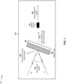
- Fig. 1 is a diagram of an overview of an example implementation 100 described herein.
- example implementation 100 includes a sensor system 110.
- Sensor system 110 may be a portion of an optical system and may provide an electrical output corresponding to a sensor determination.
- Sensor system 110 includes an optical filter structure 120, which includes an optical filter 130, and an optical sensor 140.
- optical filter structure 120 may include an optical filter 130 that performs a passband filtering functionality.
- an optical filter 130 may be aligned to an array of sensor elements of optical sensor 140.
- implementations, described herein may be described in terms of an optical filter in a sensor system, implementations described herein may be used in another type of system, may be used external to a sensor system, or in other configurations.
- an input optical signal is directed toward optical filter structure 120 at one or more angles of incidence, 0.
- input optical signals 150-1 and 150-2 may be directed toward optical filter 120 at angles of incidence ⁇ 0 (e.g., a configured angle of incidence) and 0.
- the input optical signal may include, but is not limited to, light associated with a particular spectral range (e.g., a spectral range centered at approximately 900 nm, such as a spectral range of 800 nm to 1000 nm; a spectral range of 800 nm to 1600 nm; a spectral range between 800nm and 1100nm; a spectral range between 1400 nm and 1600 nm, such as with a peak wavelength of 1550 nm; a spectral range of 500 nm to 5500 nm; or another spectral range).
- a particular spectral range e.g., a spectral range centered at approximately 900 nm, such as a spectral range of 800 nm to 1000 nm; a spectral range of 800 nm to 1600 nm; a spectral range between 800nm and 1100nm; a spectral range between 1400 nm and 1600 nm
- a first portion of the optical signal with a first spectral range is not passed through by optical filter 130 and optical filter structure 120.
- dielectric filter stacks of dielectric thin film layers which may include high index material layers and low index material layers of optical filter 130, may cause the first portion of light to be reflected in a first direction, to be absorbed, or the like.
- the first portion of light may be a threshold portion of light incident on optical filter 130 not included in a bandpass of optical filter 130, such as greater than 95% of light not within a particular spectral range centered at approximately 900 nm.
- a second portion of the optical signal is passed through by optical filter 130 and optical filter structure 120.
- optical filter 130 may pass through the second portion of light with a second spectral range in a second direction toward optical sensor 140.
- the second portion of light may be a threshold portion of light incident on optical filter 130 within a bandpass of optical filter 130, such as greater than 50% of incident light in a spectral range centered at approximately 900 nm.
- the second portion of light may pass through the optical filter 130 with less than a threshold angle shift, as described in more detail herein.
- optical sensor 140 may provide an output electrical signal 180 for sensor system 110, such as for use in imaging, ambient light sensing, detecting the presence of an object, performing a measurement, or facilitating communication, among other examples.
- another arrangement of optical filter 130 and optical sensor 140 may be utilized. For example, rather than passing the second portion of the optical signal collinearly with the input optical signal, optical filter 130 may direct the second portion of the optical signal in another direction toward a differently located optical sensor 140.
- Fig. 1 is provided as an example. Other examples may differ from what is described with regard to Fig. 1 .
- Fig. 2 is a diagram of an example optical filter 200.
- the optical filter 200 may be an optical interference filter and/or may comprise at least one of a spectral filter, a multispectral filter, a bandpass filter, a blocking filter, a long-wave pass filter, a short-wave pass filter, a dichroic filter, a linear variable filter, a circular variable filter, a Fabry-Perot filter, a Bayer filter, a plasmonic filter, a photonic crystal filter, a nanostructure or metamaterial filter, an absorbent filter, a beam splitter, a polarizing beam splitter, a notch filter, an anti-reflection filter, a reflector, or a mirror, among other examples.
- Fig. 2 shows an example stack up of the optical filter 200.
- the optical filter 200 includes a substrate 210 and a set of layers 220.
- the substrate 210 may comprise a glass substrate, a polymer substrate, a polycarbonate substrate, a metal substrate, a silicon (Si) substrate, a germanium (Ge) substrate, or an active device wafer (e.g., that comprises a photodiode (PD), a PD array, an avalanche photodiode (APD), an APD array, a charge-coupled device (CCD) sensor, and/or a complementary metal oxide semiconductor (CMOS) sensor, among other examples).
- a thickness of the substrate 210 may be greater than or equal to 20 microns ( ⁇ m), 50 ⁇ m, and/or 500 ⁇ m. Additionally, or alternatively, the thickness of the substrate may be less than or equal to a particular thickness threshold.
- the particular thickness threshold for example, may be less than or equal to 5 millimeters (mm).
- the set of layers 220 may be disposed on (e.g., directly on) the substrate 210 and may include one or more subsets of layers.
- the set of layers 220 may include a first subset of layers 230 (e.g., a first subset of layers 230-1 through 230-( N +1) ( N ⁇ 1)) (also referred to herein as A layers) and a second subset of layers 240 (e.g., a second subset of layers 240-1 through 240- N ) (also referred to herein as B layers).
- the first subset of layers 230 and the second subset of layers 240 may be arranged in a particular order (e.g., an alternating layer order), such as an ( A - B ) m ( m ⁇ 1) order, an ( A - B ) m - A order, a ( B - A ) m order, a B -( B - A ) m order, or another order.
- a particular order e.g., an alternating layer order
- the first subset of layers 230 and the second subset of layers 240 are positioned in an ( A-B ) N - A order with an A layer (e.g., layer 230-1) disposed at a surface (e.g., a top surface) of the optical filter 200 and an A layer (e.g., layer 230-( N +1)) disposed on a surface (e.g., a top surface) of the substrate 210.
- a layer e.g., layer 230-1
- the set of layers 220 may be disposed on a single surface (e.g., the top surface) of the substrate 210 (e.g., as shown in Fig. 2 ).
- a first portion of the set of layers 220 may be disposed on a first surface (e.g., the top surface) of the substrate 210
- a second portion of the set of layers 220 may be disposed on a second surface (e.g., a bottom surface) of the substrate 210.
- a first portion of the first subset of layers 230 and a first portion of the second subset of layers 240 may be arranged in a first particular order on the first surface of the substrate 210, and a second portion of the first subset of layers 230 and a second portion of the second subset of layers 240 may be arranged in a second particular order on the second surface of the substrate 210.
- one or more other layers may be included in the optical filter 200, such as one or more protective layers, one or more cap layers (e.g., to provide environmental protection to the set of layers 220), and/or one or more layers to provide one or more other filtering functionalities (e.g., a blocker or an anti-reflection coating, among other examples).
- an additional layer e.g., a cap layer
- a dielectric layer e.g., that comprises an oxide material, such as a silicon dioxide (SiO 2 ) material, a zirconium dioxide (ZrO 2 ) material, and/or an yttrium oxide (Y 2 O 3 ) material; a nitride material, such as a silicon nitride (Si 3 N 4 ) material, a titanium nitride (TiN) material, and/or a zirconium nitride (ZrN) material; and/or another material that provides environmental protection), may be disposed on a surface (e.g., a top surface) of the set of layers 220.
- a dielectric layer e.g., that comprises an oxide material, such as a silicon dioxide (SiO 2 ) material, a zirconium dioxide (ZrO 2 ) material, and/or an yttrium oxide (Y 2 O 3 ) material
- a first additional layer may be disposed on a surface (e.g., a top surface) of the first portion of the set of layers 220 and a second additional layer may be disposed on a surface (e.g., a bottom surface) of the second portion of the set of layers 220.
- the first subset of layers 230 may comprise an aluminum nitride (AlN) material.
- each layer 230, of the first subset of layers 230 may comprise an AlN material.
- the second subset of layers 240 may comprise at least one other material (e.g., at least one material other than an AlN material), such as at least one of a silicon (Si) material, a silicon and hydrogen (SiH) material, a hydrogenated silicon (Si:H) material, a hydrogenated silicon with helium (Si:H-He) material, an amorphous silicon (a-Si) material, a silicon nitride (SiN) material, a germanium (Ge) material, a hydrogenated germanium (Ge:H) material, a silicon germanium (SiGe) material, a hydrogenated silicon germanium (SiGe:H) material, a silicon carbide (SiC) material, a hydrogenated silicon carbide (SiC:H) material, a silicon
- a stress (e.g., a net stress) of the first subset of layers 230 may between -1000 and 800 MPa (e.g., greater than or equal to -1000 MPa and less than or equal to 800 MPa). Additionally, or alternatively, a stress of each layer 230, of the first subset of layers 230, may be between -1000 and 800 MPa. That is, a stress of a particular layer 230, of the first subset of layers 230, may be between -1000 and 800 MPa and a stress of another particular layer 230, of the first subset of layers 230, may be between -1000 and 800 MPa.
- the stress of the particular layer 230 may be the same as, or different than, the stress of the other particular layer 230.
- the stress of the particular layer 230 may be tensile (e.g., greater than or equal to 0 MPa) and the stress of the other particular layer 230 may be compressive (e.g., less than 0 MPa), or vice versa.
- a stress (e.g., a net stress) of the set of layers 220 may be approximately zero (0) MPa (e.g., within a tolerance, wherein the tolerance is less than or equal to 5 MPa).
- at least one of the first subset of layers 230 and the second subset of layers 240 may comprise tensile material, and another of the first subset of layers 230 and the second subset of layers 240 may comprise compressive material (e.g., to cause the stress of the set of layers 220 to be approximately zero MPa).
- the first subset of layers 230 may comprise a tensile material
- the second subset of layers 240 may comprise a compressive material, or vice versa.
- the first subset of layers 230 may comprise a tensile AlN material
- the second subset of layers 240 may comprise at least one compressive other material (e.g., at least one of a compressive Si material, a compressive Si:H material, a compressive Si:H-He material, or a compressive a-Si material, among other examples).
- a stress (e.g., a net stress) of the set of layers 220 may be approximately equal to a particular amount of stress (e.g., within a tolerance, wherein the tolerance is less than or equal to 5 MPa).
- the first subset of layers 230 and the second subset of layers 240 may comprise a particular configuration of compressive materials and/or tensile materials, such that the stress of the set of layers 230 is equal to a particular amount of stress, such as 350 MPa.
- each layer of the set of layers 220 may be associated with a particular thickness.
- a layer of the first subset of layers 230 or the second subset of layers 240 may have a thickness of between 5 and 2000 nm.
- the first subset of layers 230 or the second subset of layers 240 may be associated with multiple thicknesses, such as a first thickness for the first subset of layers 230 and a second thickness for the second subset of layers 240, a first thickness for a first portion of the first subset of layers 230 and a second thickness for a second portion of the first subset of layers 230, or a first thickness for a first portion of the second subset of layers 240 and a second thickness for a second portion of the second subset of layers 240, among other examples.
- a layer thickness and/or a quantity of layers may be selected based on an intended set of optical characteristics of the optical filter 200, such as an intended passband, an intended transmissivity, and/or another optical characteristic.
- the layer thickness and/or the quantity of layers may be selected to permit optical filter 200 to be utilized for (e.g., to pass light associated with) a spectral range of between 800 to 1000 nm (e.g., with a center wavelength of approximately 900 nm), a spectral range between 800 nm and 1600 nm, a spectral range between 800nm and 1100nm, a spectral range between 1400 nm and 1600 nm (e.g., with a peak wavelength of 1550 nm), a spectral range between 500 and 5500 nm, or another spectral range.
- the set of layers 230 may be configured to pass a threshold percentage of light associated with a particular spectral range.
- the set of layers 230 may be configured to pass a threshold percentage of light associated with a spectral range of between 800 and 1000 nm (e.g., with a center wavelength of approximately 900 nm).
- the threshold range for example, may be greater than or equal to 85%.
- an extinction coefficient of the first subset of layers 230 may be less than 0.001 for light that has a wavelength that is between 500 and 5500 nm.
- the first subset of layers 230 may have a first refractive index with a first value and the second subset of layers 240 may have a second refractive index with a second value (e.g., that is different than the first value).
- a refractive index of the first subset of layers 230 may be between 1.9 and 2.2 for light that has a wavelength that is between 500 and 5500 nm and/or a refractive index of the second subset of layers 240 may be between 3.5 and 3.9 for light that has a wavelength that is between 500 and 5500 nm.
- the optical filter 200 may have an effective refractive index greater than or equal to 95% of a highest value of the first value and the second value.
- the first subset of layers 230 and the second subset of layers 240 may be sized to achieve an effective refractive index of, for example, greater than or equal to 95% of a highest value of the first value and the second value.
- the optical filter 200 may have an effective refractive index greater than or equal to 100% of the highest value of the first value and the second value (e.g., up to 110%, 120%, 130%, 140%, or 150% of the highest value).
- the effective refractive index may be greater than or equal to 3.7, 4.0, 4.5, 5.0, and/or 5.5 when the refractive index of the second subset of layers 240 is between 3.5 and 3.9 and greater than the refractive index of the first subset of layers 230.
- the set of layers 230 may be formed using a sputtering process.
- the set of layers 230 may be formed using a magnetron sputtering process (e.g., a pulsed-magnetron sputtering process) to sputter the first subset of layers 230 and/or the second subset of layers 240 (e.g., in an alternating layer order) on the substrate 210.
- a magnetron sputtering process e.g., a pulsed-magnetron sputtering process
- the optical filter 200 may be manufactured. Further details relating to manufacturing of the optical filter 200 are described herein in relation to Fig. 3 .
- Fig. 2 is provided as an example. Other examples may differ from what is described with regard to Fig. 2 .
- Fig. 3 is a diagram of an example 300 of a sputter deposition system for manufacturing an optical filter described herein (e.g., optical filter 200).
- the sputter deposition system may be used to enable a sputtering process, such as a magnetron sputtering process.
- example 300 includes a vacuum chamber 310, a substrate 320 (e.g., that corresponds to substrate 210 described herein in relation to Fig. 2 ), a cathode 330, a target 331, a cathode power supply 340, an anode 350, a plasma activation source (PAS) 360, and a PAS power supply 370.
- the target 331 may include an aluminum (Al) material.
- the PAS power supply 370 may be utilized to power the PAS 360 and may include a radio frequency (RF) power supply.
- the cathode power supply 340 may be utilized to power cathode 330 and may include a pulsed direct current (DC) power supply.
- DC pulsed direct current
- the target 331 may be sputtered in the presence of nitrogen gas (N 2 ) and/or an inert gas (e.g., that includes argon (Ar), helium (He), and/or neon (Ne)) to deposit aluminum nitride (AlN) as at least one layer on the substrate 320.
- N 2 nitrogen gas
- an inert gas e.g., that includes argon (Ar), helium (He), and/or neon (Ne)
- AlN aluminum nitride
- the N 2 gas and the inert gas may each be supplied to the vacuum chamber 310, which may cause sputtering of the target 331 to form a first set of layers that comprise AlN on the substrate 320 (e.g., as further described herein).
- the first set of layers may be formed on the substrate in alternation with a second set of layers that comprise at least one other material, such as a second set of layers that comprises Si, Si:H, Si:H-He, a-Si, and/or any other material described herein (e.g., in relation to the second subset of layers 240 described herein in relation to Fig. 2 ) to form a formation of layers.
- a second set of layers that comprises Si, Si:H, Si:H-He, a-Si, and/or any other material described herein (e.g., in relation to the second subset of layers 240 described herein in relation to Fig. 2 ) to form a formation of layers.
- the second set of layers may be formed on the substrate (e.g., in a similar manner as further described herein) by supplying, for example, another gas (e.g., hydrogen gas (H 2 )) and the inert gas (e.g., that includes Ar, He, and/or Ne) to the vacuum chamber 310 to cause sputtering of another target (e.g., a silicon target) to form the second set of layers (e.g., that comprise, in this example, Si:H or Si:H-He).
- another gas e.g., hydrogen gas (H 2 )
- the inert gas e.g., that includes Ar, He, and/or Ne
- the formation of layers may be arranged in a particular layer order (e.g., an alternating layer order of high refractive index and low refractive index layers), such that an effective refractive index of the formation of layers is greater than or equal to 95% of a value of the highest refractive index material (e.g., up to 110%, 120%, 130%, 140%, or 150%).
- the effective refractive index may be greater than or equal to 3.7, 4.0, 4.5, 5.0, and/or 5.5 (e.g., when the second subset of layers has a refractive index that is between 3.5 and 3.9 and greater than a refractive index of the first subset of layers).
- the inert gas may be provided into the vacuum chamber 310 via the anode 350 and/or the PAS 360.
- the N 2 gas may be introduced into the vacuum chamber 310 through the PAS 360, which serves to activate the N 2 gas.
- the cathode 330 may cause the N 2 gas activation (e.g., in this case, the N 2 gas may be introduced from another part of the vacuum chamber 310) or the anode 350 may cause the N 2 gas activation (e.g., in this case, the N 2 gas may be introduced into the vacuum chamber 310 by the anode 350).
- the PAS 360 may be located within a threshold proximity of the cathode 330, allowing plasma from the PAS 360 and plasma from the cathode 330 to overlap.
- the use of the PAS 360 allows AlN to be deposited at a relatively high deposition rate.
- AlN may be deposited at a deposition rate of approximately 0.05 nm/s to approximately 2.0 nm/s, at a deposition rate of approximately 0.5 nm/s to approximately 1.2 nm/s, at a deposition rate of approximately 0.8 nm/s, or a similar rate.
- a stress of an AlN layer may be adjusted based on controlling a composition of the inert gas and/or an amount of the inert gas that is supplied to the vacuum chamber 310.
- the inert gas includes Ar
- an amount of Ar in the inert gas and/or an amount of the inert gas supplied to the vacuum chamber 310 may be controlled to cause a stress of the AlN layer to be between -230 and 800 MPa.
- an amount of Ar in the inert gas and/or an amount of the inert gas supplied to the vacuum chamber 310 may be controlled to cause a stress (e.g., a net stress) of the first set of layers that comprise AlN to be between -230 and 800 MPa.
- a stress e.g., a net stress
- the inert gas includes He and/or Ne
- an amount of He and/or Ne in the inert gas and/or an amount of the inert gas supplied to the vacuum chamber 310 may be controlled to cause a stress of the AlN layer to be between -1000 and 150 MPa.
- an amount of He and/or Ne in the inert gas and/or an amount of the inert gas supplied to the vacuum chamber 310 may be controlled to cause a stress of the first set of layers that comprise AlN to be between -1000 and 150 MPa.
- the sputtering process is described, herein, in terms of a particular geometry and a particular implementation, other geometries and other implementations are possible.
- the N 2 gas may be injected from another direction and/or from a gas manifold in a threshold proximity to the cathode 330, among other examples.
- different relative concentrations of AlN may also be achieved using different materials, different manufacturing processes, or the like.
- Fig. 3 is provided as an example. Other examples may differ from what is described with regard to Fig. 3 .
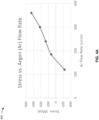
- Figs. 4A-4B are diagrams of example plots 400 that show a stress of an AlN layer formed using a sputtering process described herein (e.g., a magnetron sputtering process).
- a stress of an AlN layer may be configured to be between -230 and 650 MPa when an inert gas that includes Ar is supplied (e.g., to the vacuum chamber 310 of the sputter deposition system described herein in relation to Fig. 3 ) at a flow rate of between 120 and 370 standard cubic centimeters per minute (sccm).
- sccm standard cubic centimeters per minute
- a stress of an AlN layer may be configured to be between -950 and 175 MPa when an inert gas that includes He is supplied (e.g., to the vacuum chamber 310 of the sputter deposition system described herein in relation to Fig. 3 ) at a flow rate of between 0 and 500 sccm.
- an inert gas that includes Ar is also supplied (e.g., to the vacuum chamber 310 of the sputter deposition system described herein in relation to Fig. 3 ) at a flow rate of between 120 and 370 sccm.
- FIGS. 4A-4B are provided as an example. Other examples may differ from what is described with regard to Figs. 4A-4B .
- Fig. 5 is a diagram of an example plot 500 of an extinction coefficient (k) and a refractive index (r) of a set of AlN layers formed using a sputtering process described herein (e.g., a magnetron sputtering process).
- the extinction coefficient may be less than 0.001 for light that has a wavelength that is between 500 and 2000 nm.
- the refractive index may be less than 2.2 for light that has a wavelength that is between 500 and 2000 nm.
- Fig. 5 is provided as an example. Other examples may differ from what is described with regard to Fig. 5 .
- Fig. 6 is a diagram of an example plot 600 that shows a transmittance performance of an optical filter (e.g., the optical filter 200) described herein.
- the optical filter comprises a set of layers (e.g., the set of layers 220) that includes a first subset of layers (e.g., the first subset of layers 230) that comprise an AlN material and a second subset of layers (e.g., the second subset of layers 240) that comprise an Si:H material.
- the optical filter may transmit greater than approximately 85% (with a peak of approximately 92%) of light that has a wavelength that is between 920 and 960 nm.
- an alternative optical filter that comprises a set of layers that includes a first subset of layers that comprise a Ta 2 O 5 material and a second subset of layers that comprise an Si:H material may transmit greater than approximately 60% (with a peak of approximately 67%) of light that has a wavelength that is between 920 and 960 nm. Accordingly, the optical filter described herein has an improved transmittance performance as compared to the alternative optical filter for the spectral range of between 920 and 960 nm.
- Fig. 6 is provided as an example. Other examples may differ from what is described with regard to Fig. 6 .
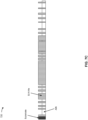
- Figs. 7A-7C are diagrams 700/710/720 of optical and physical characteristics of an example implementation described herein.
- diagram 700 shows an angle shift performance of an optical filter (e.g., optical filter 200 described herein).
- An angle shift at a center wavelength of the optical interference filter may be less than 1.0% of the center wavelength for angles of incidence (shown as ⁇ in Fig. 7A ) between 0 degrees and 30 degrees.
- the optical filter when configured for a center wavelength at 940 nanometers (nm), the optical filter may have an angle shift of, for example, less than 9.4 nm at angles of incidence of up to 30 degrees.
- optical filter may have an angle shift of less than 7.0 nm at angles of incidence of up to 30 degrees.
- the optical filter may achieve an effective refractive index that is, for example, greater than or equal to 3.7, 4.0, 4.5, 5.0, and/or 5.5.
- the optical filter may achieve a transmittance, at the center wavelength, of greater than a transmittance threshold, such as greater than 80%, greater than 85%, greater than 90%, and/or greater than 95% (e.g., of a peak transmissivity of the optical filter at angles of incidence of between 0 to 30 degrees).
- the optical filter may achieve a ripple of less than +/-10%, less than +/-5%, or less than +/-1%, where the ripple represents a deviation in transmittance across the passband at angles of incidence of between 0 and 30 degrees.
- diagrams 710 and 720 show an example stack up and an example of layer thicknesses for the optical filter.
- the optical filter is manufactured by alternating layers comprising an AlN material (e.g., with a refractive index between 1.9 and 2.2 for light that has a wavelength that is between 500 and 5500 nm) and layers comprising an Si:H-He material (e.g., with a refractive index between 3.5 and 3.9 for light that has a wavelength that is between 500 and 5500 nm).
- the optical filter includes one or two "thick layers" with greater than a threshold thickness (e.g., a thickness greater 200% more than a next thickest layer after the one or more two layers and less than, for example, 500% more than a next thickest layer).
- a threshold thickness e.g., a thickness greater 200% more than a next thickest layer after the one or more two layers and less than, for example, 500% more than a next thickest layer.
- the optical filter may include two thick layers and the thick layers may deviate by between 10% and 25%.
- a thickness of a smaller of the two thick layers may be smaller than a thickness of a larger of the two thick layers by between 10% and 25%.
- FIGS. 7A-7C are provided merely as an example. Other examples may differ from what is described with regard to Figs. 7A-7C .
- Figs. 8A-8C are diagrams 800/810/820 of optical and physical characteristics of an example implementation described herein.
- diagram 800 shows an angle shift performance of an optical filter (e.g., optical filter 200 described herein).
- An angle shift at a center wavelength of the optical interference filter may be less than 1.0% of the center wavelength for angles of incidence (shown as ⁇ in Fig. 8A ) between 0 degrees and 30 degrees.
- the optical filter when configured for a center wavelength at 940 nanometers (nm), the optical filter may have an angle shift of, for example, less than 9.4 nm at angles of incidence of up to 30 degrees.
- optical filter may have an angle shift of less than 7.0 nm at angles of incidence of up to 30 degrees.
- the optical filter may achieve an effective refractive index that is, for example, greater than or equal to 3.7, 4.0, 4.5, 5.0, and/or 5.5.
- the optical filter may achieve a transmittance, at the center wavelength, of greater than a transmittance threshold, such as greater than 80%, greater than 85%, greater than 90%, and/or greater than 95% (e.g., of a peak transmissivity of the optical filter at angles of incidence of between 0 to 30 degrees).
- the optical filter may achieve a ripple of less than +/-10%, less than +/-5%, or less than +/-1%, where the ripple represents a deviation in transmittance across the passband at angles of incidence of between 0 and 30 degrees.
- diagrams 810 and 820 show an example stack up and an example of layer thicknesses for the optical filter.
- the optical filter is manufactured by alternating layers comprising an AlN material (e.g., with a refractive index between 1.9 and 2.2 for light that has a wavelength that is between 500 and 5500 nm) and layers comprising an Si:H-He material (e.g., with a refractive index between 3.5 and 3.9 for light that has a wavelength that is between 500 and 5500 nm).
- the optical may also include an additional layer (e.g., a cap layer, as described herein) comprising an SiO 2 material.
- FIGS. 8A-8C are provided merely as an example. Other examples may differ from what is described with regard to Figs. 8A-8C .
- the term "component” is intended to be broadly construed as hardware, firmware, or a combination of hardware and software. It will be apparent that systems and/or methods described herein may be implemented in different forms of hardware, firmware, and/or a combination of hardware and software. The actual specialized control hardware or software code used to implement these systems and/or methods is not limiting of the implementations. Thus, the operation and behavior of the systems and/or methods are described herein without reference to specific software code - it being understood that software and hardware can be used to implement the systems and/or methods based on the description herein.
- satisfying a threshold may, depending on the context, refer to a value being greater than the threshold, greater than or equal to the threshold, less than the threshold, less than or equal to the threshold, equal to the threshold, not equal to the threshold, or the like.
- a, b, or c is intended to cover a, b, c, a-b, a-c, b-c, and a-b-c, as well as any combination with multiple of the same item.
- the terms “has,” “have,” “having,” or the like are intended to be open-ended terms. Further, the phrase “based on” is intended to mean “based, at least in part, on” unless explicitly stated otherwise. Also, as used herein, the term “or” is intended to be inclusive when used in a series and may be used interchangeably with “and/or,” unless explicitly stated otherwise (e.g., if used in combination with “either” or “only one of').
Landscapes
- Chemical & Material Sciences (AREA)
- Physics & Mathematics (AREA)
- Organic Chemistry (AREA)
- Materials Engineering (AREA)
- Mechanical Engineering (AREA)
- Metallurgy (AREA)
- Engineering & Computer Science (AREA)
- Chemical Kinetics & Catalysis (AREA)
- General Physics & Mathematics (AREA)
- Optics & Photonics (AREA)
- Fluid Mechanics (AREA)
- Spectroscopy & Molecular Physics (AREA)
- Optical Filters (AREA)
Abstract
Description
- An optical device may be utilized to capture information concerning light. For example, the optical device may capture information relating to a set of wavelengths associated with the light. The optical device may include a set of sensor elements (e.g., optical sensors, spectral sensors, and/or image sensors) that capture the information. For example, an array of sensor elements may be utilized to capture information relating to multiple wavelengths. The array of sensor elements may be associated with an optical filter. The optical filter may include a passband associated with a first wavelength range of light that is passed to the array of sensor elements. The optical filter may be associated with blocking a second wavelength range of light from being passed to the array of sensor elements.
- In some implementations, an optical interference filter includes a substrate; and a set of layers that are disposed on the substrate, wherein the set of layers includes: a first subset of layers; and a second subset of layers; wherein: each of the first subset of layers comprises an aluminum nitride (AlN) material, a stress of each of the first subset of layers is between -1000 and 800 megapascals, the first subset of layers has a first refractive index with a first value, each of the second subset of layers comprises at least one other material, the second subset of layers has a second refractive index with a second value that is different than the first value, and the optical interference filter has an effective refractive index greater than or equal to 95% of a highest value of the first value and the second value.
- An angle shift at a center wavelength of the optical interference filter may be less than 1.0% of the center wavelength for angles of incidence between 0 degrees and 30 degrees.
- A net stress of the set of layers may be approximately zero megapascals.
- A first subset of layers and a second subset of layers may be disposed on the substrate in an alternating layer order.
- The at least one other material may include at least one of: a silicon (Si) material; a hydrogenated silicon (Si:H) material; a hydrogenated silicon with helium (Si:H-He) material; a silicon and hydrogen material (SiH) material; an amorphous silicon (a-Si) material; a silicon nitride (SiN) material; a germanium (Ge) material; a hydrogenated germanium (Ge:H) material; a silicon germanium (SiGe) material; a hydrogenated silicon germanium (SiGe:H) material; a silicon carbide (SiC) material; a hydrogenated silicon carbide (SiC:H) material; a silicon dioxide (SiO2) material; a tantalum pentoxide (Ta2O5) material; a niobium pentoxide (Nb2O5) material; a niobium titanium oxide (NbTiOx) material; a niobium tantalum pentoxide (Nb2-xTaxO5) material; a titanium dioxide (TiO2) material; an aluminum oxide (Al2O3) material; a zirconium oxide (ZrO2) material; an yttrium oxide (Y2O3) material; or a hafnium oxide (HfO2) material.
- An additional layer may be disposed on the set of layers, wherein the additional layer may comprise a silicon dioxide (SiO2) material.
- The optical interference filter may be configured to pass light associated with a spectral range of between 800 to 1600 nanometers.
- In some implementations, an optical interference filter includes a set of layers that includes: a first subset of layers; and a second subset of layers, wherein: each of the first subset of layers comprises an AlN material, the first subset of layers having a first refractive index with a first value, each of the second subset of layers comprises a hydrogenated silicon with helium (Si:H-He) material, the second subset of layers having a second refractive index with a second value that is greater than the first value, and the optical interference filter has an effective refractive index greater than or equal to 95% of the second value.
- One of the first subset of layers and the second subset of layers may comprise tensile material, and wherein another of the first subset of layers and the second subset of layers may comprise compressive material.
- A net stress of the set of layers may be approximately zero megapascals.
- A net stress of the set of layers may be approximately equal to a particular amount of stress.
- The first value may be between 1.9 and 2.2 for light that has a wavelength that is between 500 and 5500 nanometers; and the second value may be between 3.5 and 3.9 for light that has a wavelength that is between 500 and 5500 nanometers.
- An additional layer may be disposed on the set of layers, wherein the additional layer may comprise a silicon dioxide (SiO2) material.
- The optical interference filter, for angles of incidence between 0 degrees and 30 degrees, may have less than a 7.0 nanometer (nm) angle shift at a wavelength that is 940 nm and an effective refractive index that may be greater than or equal to 3.7.
- An angle shift at a center wavelength of the optical interference filter may be less than 1.0% of the center wavelength for angles of incidence between 0 degrees and 30 degrees.
- The center wavelength may be 940 nanometers.
- The optical interference filter may be associated with a transmissivity of between 90% and 100% of a peak transmissivity of the optical interference filter and for angles of incidence of between 0 degrees and 30 degrees.
- In some implementations, a method includes supplying an inert gas to a chamber, wherein the inert gas includes at least one of argon (Ar) or helium (He); supplying nitrogen gas (N2) to the chamber; and causing, based on supplying the inert gas and the N2 gas, sputtering of an aluminum (Al) target to form a first set of layers that comprise AlN on a substrate, wherein: the first set of layers are formed on the substrate in alternation with a second set of layers to form a formation of layers, the second set of layers comprise Si:H-He, and the formation of layers has an effective refractive index that is greater than or equal to 3.7.
- The inert gas may include He; a stress of the first set of layers may be between -1000 and 150 megapascals; and a refractive index of the first set of layers may be between 1.9 and 2.2 for light that has a wavelength that is between 500 and 5500 nanometers.
- The inert gas may include helium (He), wherein the method may further comprises: supplying hydrogen (H2) gas to the chamber; and causing, based on supplying the inert gas and the H2 gas, sputtering of a silicon (Si) target to form the second set of layers that comprise Si:H-He.
-
-
Fig. 1 is a diagram of an overview of an example implementation described herein. -
Fig. 2 is a diagram of an example optical filter described herein. -
Fig. 3 is a diagram of an example of a sputter deposition system for manufacturing an optical filter described herein. -
Figs. 4A-4B are diagrams of example plots that show a stress of an AlN layer formed using a sputtering process described herein. -
Fig. 5 is a diagram of an example plot of an extinction coefficient and a refractive index of a set of AlN layers formed using a sputtering process described herein. -
Fig. 6 is a diagram of an example plot that shows a transmittance performance of an optical filter described herein. -
Figs. 7A-7C are diagrams of optical and physical characteristics of an example implementation described herein. -
Figs. 8A-8C are diagrams of optical and physical characteristics of an example implementation described herein. - The following detailed description of example implementations refers to the accompanying drawings. The same reference numbers in different drawings may identify the same or similar elements. The following description uses a spectrometer as an example. However, the techniques, principles, procedures, and methods described herein may be used with any sensor, including but not limited to other optical sensors and spectral sensors.
- An optical filter may be manufactured by forming one or more layers on a substrate. For example, a conventional optical filter may include alternating layers of at least a first material, a second material, and a third material (e.g., alternating layers of a hydrogenated silicon (Si:H) material, a silicon dioxide (SiO2) material, and a tantalum pentoxide (Ta2O5) material) to allow the conventional optical filter to pass a threshold percentage of light (e.g., at least 65% of light) associated with a particular spectral range (e.g., a spectral range of between 800 to 1600 nanometers (nm)). However, forming alternating layers of at least three materials is complex and can lead to formation of low quality layers, which introduces defects or allows defects to propagate through the conventional optical filter. This can degrade a performance, manufacturability, and/or a reliability of the conventional optical filter.
- Further, in many cases, a stress of each of the layers of the one or more layers of the conventional optical filter is compressive (e.g., the stress of the layers is less than 0 megapascals (MPa)), which causes a stress (e.g., a net stress) of the one or more layers to be compressive. Consequently, this causes the conventional optical filter to bow (e.g., to bend). This causes the one or more layers to suffer from coating runoff, which affects a performance of the conventional optical filter. This also causes the conventional optical filter to be more fragile (e.g., as compared to a flat optical filter) and/or makes transporting, handling, and/or use of the conventional optical filter difficult.
- Additionally, a filter performance of the conventional optical filter may be degraded when an angle of incidence (AOI) of light directed toward the optical filter changes from a configured incidence (e.g., 0 degrees (normal), 30 degrees, 45 degrees, and/or the like) to a threshold angle of incidence (e.g., greater than approximately 10 degrees deviation from the configured incidence, 20 degrees deviation from the configured incidence, and/or 30 degrees deviation from the configured incidence). For example, the conventional optical filter may shift toward lower wavelengths at an increase in an angle of incidence. In this way, the conventional optical filter may pass unwanted or undesired light, which may affect a sensing accuracy of an optical sensor that receives the passed light.
- Angle shift may be related to an effective refractive index of an optical filter (e.g., a bandpass filter). For example, a higher effective refractive index correlates with a lower angle shift. The effective refractive index is calculable from component refractive indices of component materials of the optical filter. For example, the effective refractive index, for an optical filter with mirrors formed from alternating high refractive index component material layers and low refractive index component material layers, may be calculated based at least in part on a set of equations of the forms:


- Another calculation for effective refractive index may relate to an observed wavelength shift (e.g., an angle shift) of the optical filter. For example, a wavelength shift of an optical filter (e.g., a bandpass filter) at a particular angle of incidence may be determined based on an equation of the form:


- The above equations show that higher effective refractive indices result in lower angle shifts for filters. However, a limit to the effective refractive index of the filter is less than a refractive index of a highest refractive index material in the filter (Eq. 3).
- Some implementations described herein provide an optical filter that includes a set of layers disposed on the substrate. The set of layers may include a first subset of layers that comprise an aluminum nitride (AlN) material and a second subset of layers that comprise at least one other material (e.g., at least one material that is not an AlN material), such as a hydrogenated silicon with helium (Si:H-He) material, arranged in an alternating layer order. In some implementations, the optical filter passes a threshold percentage of light (e.g., at least 90% of light) associated with a particular spectral range (e.g., a spectral range of between 800 to 1600 nm). In this way, the optical filter provides an improved transmittance performance as compared to a conventional optical filter. Further, the optical filter includes just two alternating layers, which reduces a complexity associated with forming the set of layers. This reduces a likelihood of formation of low quality layers, and therefore reduces a likelihood of defects being introduced in or allowed to propagate through the optical filter. Therefore, a performance, manufacturability, and/or a reliability of the optical filter is improved as compared to that of a conventional optical filter.
- In some implementations, a stress of the first subset of layers that comprise the AlN material may be between -1000 and 800 MPa. Accordingly, in some implementations, the stress of the AlN material may be configured to be tensile (e.g., greater than or equal to 0 MPa) when a stress of the second subset of layers is compressive, or vice versa. In this way, an amount of bowing caused by the set of layers disposed on the substrate may be minimized (e.g., by balancing a stress of compressive layers and a stress of tensile layers of the optical filter). For example, one of the first subset of layers and the second subset of layers may comprise tensile material and another of the first subset of layers and the second subset of layers may comprise compressive material, which may cause the stress of the set of layers to be approximately zero MPa (e.g., within a tolerance). This minimizes an amount of bowing of the optical filter, which reduces coating runoff and thereby improves a performance of the optical filter (e.g., as compared to a conventional optical filter that suffers from bowing). This also improves a durability of the optical filter and/or makes transporting, handling, and/or use of the optical filter easier as compared to a conventional optical filter that suffers from bowing. In a specific example, such as when a diameter of the optical filter is approximately 200 millimeters (mm), some implementations described herein enable an amount of bowing of the optical filter to be less than 10 mm, less than 5 mm, and/or less than 0.1 mm, among other examples. In another example, when the optical filter is configured to pass light associated with a wavelength λ, some implementations described herein enable an amount of bowing of the optical filter to be less than λ/4, less than λ/10, and/or less than λ/100, among other examples.
- Further, some implementations described herein provide a low angle shift optical filter where an effective refractive index is greater than 95% of a refractive index of a highest refractive index material in the low angle shift optical filter. For example, the low angle shift optical filter may have an effective refractive index that takes the form:

- Additionally, or alternatively, the low angle shift optical filter may have an effective refractive index of greater than 100%, greater than 110%, greater than 120%, and/or the like of a refractive index of the highest refractive index material in the low angle shift optical filter. In this way, the low angle shift optical filter reduces an amount of unwanted or undesired light that is passed by the low angle shift optical filter, which improves a sensing accuracy of an optical sensor that receives light that is passed by the low angle shift optical filter.
-
Fig. 1 is a diagram of an overview of anexample implementation 100 described herein. As shown inFig. 1 ,example implementation 100 includes asensor system 110.Sensor system 110 may be a portion of an optical system and may provide an electrical output corresponding to a sensor determination.Sensor system 110 includes anoptical filter structure 120, which includes anoptical filter 130, and anoptical sensor 140. For example,optical filter structure 120 may include anoptical filter 130 that performs a passband filtering functionality. In another example, anoptical filter 130 may be aligned to an array of sensor elements ofoptical sensor 140. - Although some implementations, described herein, may be described in terms of an optical filter in a sensor system, implementations described herein may be used in another type of system, may be used external to a sensor system, or in other configurations.
- As further shown in
Fig. 1 , and byreference number 150, an input optical signal is directed towardoptical filter structure 120 at one or more angles of incidence, 0. For example, input optical signals 150-1 and 150-2 may be directed towardoptical filter 120 at angles of incidence θ0 (e.g., a configured angle of incidence) and 0. The input optical signal may include, but is not limited to, light associated with a particular spectral range (e.g., a spectral range centered at approximately 900 nm, such as a spectral range of 800 nm to 1000 nm; a spectral range of 800 nm to 1600 nm; a spectral range between 800nm and 1100nm; a spectral range between 1400 nm and 1600 nm, such as with a peak wavelength of 1550 nm; a spectral range of 500 nm to 5500 nm; or another spectral range). For example, an optical transmitter may direct the light towardoptical sensor 140 to permitoptical sensor 140 to perform a measurement of the light. In another example, the optical transmitter may direct another spectral range of light for another functionality, such as a testing functionality, a sensing functionality, or a communications functionality, among other examples. - As further shown in
Fig. 1 , and byreference number 160, a first portion of the optical signal with a first spectral range is not passed through byoptical filter 130 andoptical filter structure 120. For example, dielectric filter stacks of dielectric thin film layers, which may include high index material layers and low index material layers ofoptical filter 130, may cause the first portion of light to be reflected in a first direction, to be absorbed, or the like. In this case, the first portion of light may be a threshold portion of light incident onoptical filter 130 not included in a bandpass ofoptical filter 130, such as greater than 95% of light not within a particular spectral range centered at approximately 900 nm. As shown byreference number 170, a second portion of the optical signal is passed through byoptical filter 130 andoptical filter structure 120. For example,optical filter 130 may pass through the second portion of light with a second spectral range in a second direction towardoptical sensor 140. In this case, the second portion of light may be a threshold portion of light incident onoptical filter 130 within a bandpass ofoptical filter 130, such as greater than 50% of incident light in a spectral range centered at approximately 900 nm. The second portion of light may pass through theoptical filter 130 with less than a threshold angle shift, as described in more detail herein. - As further shown in
Fig. 1 , based on the second portion of the optical signal being passed tooptical sensor 140,optical sensor 140 may provide an outputelectrical signal 180 forsensor system 110, such as for use in imaging, ambient light sensing, detecting the presence of an object, performing a measurement, or facilitating communication, among other examples. In some implementations, another arrangement ofoptical filter 130 andoptical sensor 140 may be utilized. For example, rather than passing the second portion of the optical signal collinearly with the input optical signal,optical filter 130 may direct the second portion of the optical signal in another direction toward a differently locatedoptical sensor 140. - As indicated above,
Fig. 1 is provided as an example. Other examples may differ from what is described with regard toFig. 1 . -
Fig. 2 is a diagram of an exampleoptical filter 200. In some implementations, theoptical filter 200 may be an optical interference filter and/or may comprise at least one of a spectral filter, a multispectral filter, a bandpass filter, a blocking filter, a long-wave pass filter, a short-wave pass filter, a dichroic filter, a linear variable filter, a circular variable filter, a Fabry-Perot filter, a Bayer filter, a plasmonic filter, a photonic crystal filter, a nanostructure or metamaterial filter, an absorbent filter, a beam splitter, a polarizing beam splitter, a notch filter, an anti-reflection filter, a reflector, or a mirror, among other examples.Fig. 2 shows an example stack up of theoptical filter 200. As further shown inFig. 2 , theoptical filter 200 includes asubstrate 210 and a set oflayers 220. - The
substrate 210 may comprise a glass substrate, a polymer substrate, a polycarbonate substrate, a metal substrate, a silicon (Si) substrate, a germanium (Ge) substrate, or an active device wafer (e.g., that comprises a photodiode (PD), a PD array, an avalanche photodiode (APD), an APD array, a charge-coupled device (CCD) sensor, and/or a complementary metal oxide semiconductor (CMOS) sensor, among other examples). In some implementations, a thickness of thesubstrate 210 may be greater than or equal to 20 microns (µm), 50 µm, and/or 500 µm. Additionally, or alternatively, the thickness of the substrate may be less than or equal to a particular thickness threshold. The particular thickness threshold, for example, may be less than or equal to 5 millimeters (mm). - The set of layers 220 (e.g., a set of optical filter layers) may be disposed on (e.g., directly on) the
substrate 210 and may include one or more subsets of layers. For example, the set oflayers 220 may include a first subset of layers 230 (e.g., a first subset of layers 230-1 through 230-(N+1) (N ≥ 1)) (also referred to herein as A layers) and a second subset of layers 240 (e.g., a second subset of layers 240-1 through 240-N) (also referred to herein as B layers). In some implementations, the first subset oflayers 230 and the second subset oflayers 240 may be arranged in a particular order (e.g., an alternating layer order), such as an (A-B) m (m ≥ 1) order, an (A-B) m -A order, a (B-A)m order, a B-(B-A) m order, or another order. For example, as shown inFig. 2 , the first subset oflayers 230 and the second subset oflayers 240 are positioned in an (A-B) N -A order with an A layer (e.g., layer 230-1) disposed at a surface (e.g., a top surface) of theoptical filter 200 and an A layer (e.g., layer 230-(N+1)) disposed on a surface (e.g., a top surface) of thesubstrate 210. - In some implementations, the set of
layers 220 may be disposed on a single surface (e.g., the top surface) of the substrate 210 (e.g., as shown inFig. 2 ). Alternatively, a first portion of the set oflayers 220 may be disposed on a first surface (e.g., the top surface) of thesubstrate 210, and a second portion of the set oflayers 220 may be disposed on a second surface (e.g., a bottom surface) of thesubstrate 210. For example, a first portion of the first subset oflayers 230 and a first portion of the second subset oflayers 240 may be arranged in a first particular order on the first surface of thesubstrate 210, and a second portion of the first subset oflayers 230 and a second portion of the second subset oflayers 240 may be arranged in a second particular order on the second surface of thesubstrate 210. - In some implementations, one or more other layers may be included in the
optical filter 200, such as one or more protective layers, one or more cap layers (e.g., to provide environmental protection to the set of layers 220), and/or one or more layers to provide one or more other filtering functionalities (e.g., a blocker or an anti-reflection coating, among other examples). For example, in a single surface configuration, an additional layer (e.g., a cap layer), such as a dielectric layer (e.g., that comprises an oxide material, such as a silicon dioxide (SiO2) material, a zirconium dioxide (ZrO2) material, and/or an yttrium oxide (Y2O3) material; a nitride material, such as a silicon nitride (Si3N4) material, a titanium nitride (TiN) material, and/or a zirconium nitride (ZrN) material; and/or another material that provides environmental protection), may be disposed on a surface (e.g., a top surface) of the set oflayers 220. As another example, in a dual surface configuration, a first additional layer may be disposed on a surface (e.g., a top surface) of the first portion of the set oflayers 220 and a second additional layer may be disposed on a surface (e.g., a bottom surface) of the second portion of the set oflayers 220. - The first subset of
layers 230 may comprise an aluminum nitride (AlN) material. For example, eachlayer 230, of the first subset oflayers 230 may comprise an AlN material. The second subset oflayers 240 may comprise at least one other material (e.g., at least one material other than an AlN material), such as at least one of a silicon (Si) material, a silicon and hydrogen (SiH) material, a hydrogenated silicon (Si:H) material, a hydrogenated silicon with helium (Si:H-He) material, an amorphous silicon (a-Si) material, a silicon nitride (SiN) material, a germanium (Ge) material, a hydrogenated germanium (Ge:H) material, a silicon germanium (SiGe) material, a hydrogenated silicon germanium (SiGe:H) material, a silicon carbide (SiC) material, a hydrogenated silicon carbide (SiC:H) material, a silicon dioxide (SiO2) material, a tantalum pentoxide (Ta2O5) material, a niobium pentoxide (Nb2O5) material, a niobium titanium oxide (NbTiOx) material, a niobium tantalum pentoxide (Nb2-xTaxO5) material, a titanium dioxide (TiO2) material, an aluminum oxide (Al2O3) material, a zirconium oxide (ZrO2) material, an yttrium oxide (Y2O3) material, or a hafnium oxide (HfO2) material, among other examples. For example, eachlayer 240, of the second subset oflayers 240 may comprise at least one other material. - In some implementations, a stress (e.g., a net stress) of the first subset of
layers 230 may between -1000 and 800 MPa (e.g., greater than or equal to -1000 MPa and less than or equal to 800 MPa). Additionally, or alternatively, a stress of eachlayer 230, of the first subset oflayers 230, may be between -1000 and 800 MPa. That is, a stress of aparticular layer 230, of the first subset oflayers 230, may be between -1000 and 800 MPa and a stress of anotherparticular layer 230, of the first subset oflayers 230, may be between -1000 and 800 MPa. The stress of theparticular layer 230 may be the same as, or different than, the stress of the otherparticular layer 230. For example, the stress of theparticular layer 230 may be tensile (e.g., greater than or equal to 0 MPa) and the stress of the otherparticular layer 230 may be compressive (e.g., less than 0 MPa), or vice versa. - In some implementations, a stress (e.g., a net stress) of the set of
layers 220 may be approximately zero (0) MPa (e.g., within a tolerance, wherein the tolerance is less than or equal to 5 MPa). Accordingly, at least one of the first subset oflayers 230 and the second subset oflayers 240 may comprise tensile material, and another of the first subset oflayers 230 and the second subset oflayers 240 may comprise compressive material (e.g., to cause the stress of the set oflayers 220 to be approximately zero MPa). For example, the first subset oflayers 230 may comprise a tensile material, and the second subset oflayers 240 may comprise a compressive material, or vice versa. As another example, the first subset oflayers 230 may comprise a tensile AlN material, and the second subset oflayers 240 may comprise at least one compressive other material (e.g., at least one of a compressive Si material, a compressive Si:H material, a compressive Si:H-He material, or a compressive a-Si material, among other examples). In some implementations, a stress (e.g., a net stress) of the set oflayers 220 may be approximately equal to a particular amount of stress (e.g., within a tolerance, wherein the tolerance is less than or equal to 5 MPa). For example, the first subset oflayers 230 and the second subset oflayers 240 may comprise a particular configuration of compressive materials and/or tensile materials, such that the stress of the set oflayers 230 is equal to a particular amount of stress, such as 350 MPa. - In some implementations, each layer of the set of
layers 220 may be associated with a particular thickness. For example, a layer of the first subset oflayers 230 or the second subset oflayers 240 may have a thickness of between 5 and 2000 nm. In some implementations, the first subset oflayers 230 or the second subset oflayers 240 may be associated with multiple thicknesses, such as a first thickness for the first subset oflayers 230 and a second thickness for the second subset oflayers 240, a first thickness for a first portion of the first subset oflayers 230 and a second thickness for a second portion of the first subset oflayers 230, or a first thickness for a first portion of the second subset oflayers 240 and a second thickness for a second portion of the second subset oflayers 240, among other examples. Accordingly, a layer thickness and/or a quantity of layers may be selected based on an intended set of optical characteristics of theoptical filter 200, such as an intended passband, an intended transmissivity, and/or another optical characteristic. For example, the layer thickness and/or the quantity of layers may be selected to permitoptical filter 200 to be utilized for (e.g., to pass light associated with) a spectral range of between 800 to 1000 nm (e.g., with a center wavelength of approximately 900 nm), a spectral range between 800 nm and 1600 nm, a spectral range between 800nm and 1100nm, a spectral range between 1400 nm and 1600 nm (e.g., with a peak wavelength of 1550 nm), a spectral range between 500 and 5500 nm, or another spectral range. - In some implementations, the set of
layers 230 may be configured to pass a threshold percentage of light associated with a particular spectral range. For example, the set oflayers 230 may be configured to pass a threshold percentage of light associated with a spectral range of between 800 and 1000 nm (e.g., with a center wavelength of approximately 900 nm). The threshold range, for example, may be greater than or equal to 85%. In some implementations, an extinction coefficient of the first subset oflayers 230 may be less than 0.001 for light that has a wavelength that is between 500 and 5500 nm. - In some implementations, the first subset of
layers 230 may have a first refractive index with a first value and the second subset oflayers 240 may have a second refractive index with a second value (e.g., that is different than the first value). For example, a refractive index of the first subset oflayers 230 may be between 1.9 and 2.2 for light that has a wavelength that is between 500 and 5500 nm and/or a refractive index of the second subset oflayers 240 may be between 3.5 and 3.9 for light that has a wavelength that is between 500 and 5500 nm. In some implementations, theoptical filter 200 may have an effective refractive index greater than or equal to 95% of a highest value of the first value and the second value. For example, when the first subset oflayers 230 and the second subset oflayers 240 are arranged in a particular layer order (e.g., an alternating layer order of high refractive index and low refractive index layers), the first subset oflayers 230 and the second subset oflayers 240 may be sized to achieve an effective refractive index of, for example, greater than or equal to 95% of a highest value of the first value and the second value. In some implementations, theoptical filter 200 may have an effective refractive index greater than or equal to 100% of the highest value of the first value and the second value (e.g., up to 110%, 120%, 130%, 140%, or 150% of the highest value). Accordingly, for example, the effective refractive index may be greater than or equal to 3.7, 4.0, 4.5, 5.0, and/or 5.5 when the refractive index of the second subset oflayers 240 is between 3.5 and 3.9 and greater than the refractive index of the first subset oflayers 230. - In some implementations, the set of
layers 230 may be formed using a sputtering process. For example, the set oflayers 230 may be formed using a magnetron sputtering process (e.g., a pulsed-magnetron sputtering process) to sputter the first subset oflayers 230 and/or the second subset of layers 240 (e.g., in an alternating layer order) on thesubstrate 210. In this way, theoptical filter 200 may be manufactured. Further details relating to manufacturing of theoptical filter 200 are described herein in relation toFig. 3 . - As indicated above,
Fig. 2 is provided as an example. Other examples may differ from what is described with regard toFig. 2 . -
Fig. 3 is a diagram of an example 300 of a sputter deposition system for manufacturing an optical filter described herein (e.g., optical filter 200). The sputter deposition system may be used to enable a sputtering process, such as a magnetron sputtering process. - As shown in
Fig. 3 , example 300 includes avacuum chamber 310, a substrate 320 (e.g., that corresponds tosubstrate 210 described herein in relation toFig. 2 ), acathode 330, atarget 331, acathode power supply 340, ananode 350, a plasma activation source (PAS) 360, and aPAS power supply 370. Thetarget 331 may include an aluminum (Al) material. ThePAS power supply 370 may be utilized to power thePAS 360 and may include a radio frequency (RF) power supply. Thecathode power supply 340 may be utilized topower cathode 330 and may include a pulsed direct current (DC) power supply. - With regard to
Fig. 3 , thetarget 331 may be sputtered in the presence of nitrogen gas (N2) and/or an inert gas (e.g., that includes argon (Ar), helium (He), and/or neon (Ne)) to deposit aluminum nitride (AlN) as at least one layer on thesubstrate 320. For example, the N2 gas and the inert gas may each be supplied to thevacuum chamber 310, which may cause sputtering of thetarget 331 to form a first set of layers that comprise AlN on the substrate 320 (e.g., as further described herein). In some implementations, the first set of layers may be formed on the substrate in alternation with a second set of layers that comprise at least one other material, such as a second set of layers that comprises Si, Si:H, Si:H-He, a-Si, and/or any other material described herein (e.g., in relation to the second subset oflayers 240 described herein in relation toFig. 2 ) to form a formation of layers. The second set of layers may be formed on the substrate (e.g., in a similar manner as further described herein) by supplying, for example, another gas (e.g., hydrogen gas (H2)) and the inert gas (e.g., that includes Ar, He, and/or Ne) to thevacuum chamber 310 to cause sputtering of another target (e.g., a silicon target) to form the second set of layers (e.g., that comprise, in this example, Si:H or Si:H-He). - In some implementations, the formation of layers may be arranged in a particular layer order (e.g., an alternating layer order of high refractive index and low refractive index layers), such that an effective refractive index of the formation of layers is greater than or equal to 95% of a value of the highest refractive index material (e.g., up to 110%, 120%, 130%, 140%, or 150%). Accordingly, for example, the effective refractive index may be greater than or equal to 3.7, 4.0, 4.5, 5.0, and/or 5.5 (e.g., when the second subset of layers has a refractive index that is between 3.5 and 3.9 and greater than a refractive index of the first subset of layers).
- To form an AlN layer, the inert gas may be provided into the
vacuum chamber 310 via theanode 350 and/or thePAS 360. The N2 gas may be introduced into thevacuum chamber 310 through thePAS 360, which serves to activate the N2 gas. Additionally, or alternatively, thecathode 330 may cause the N2 gas activation (e.g., in this case, the N2 gas may be introduced from another part of the vacuum chamber 310) or theanode 350 may cause the N2 gas activation (e.g., in this case, the N2 gas may be introduced into thevacuum chamber 310 by the anode 350). ThePAS 360 may be located within a threshold proximity of thecathode 330, allowing plasma from thePAS 360 and plasma from thecathode 330 to overlap. The use of thePAS 360 allows AlN to be deposited at a relatively high deposition rate. In some implementations, AlN may be deposited at a deposition rate of approximately 0.05 nm/s to approximately 2.0 nm/s, at a deposition rate of approximately 0.5 nm/s to approximately 1.2 nm/s, at a deposition rate of approximately 0.8 nm/s, or a similar rate. - In some implementations, a stress of an AlN layer (e.g., after formation) may be adjusted based on controlling a composition of the inert gas and/or an amount of the inert gas that is supplied to the
vacuum chamber 310. For example, when the inert gas includes Ar, an amount of Ar in the inert gas and/or an amount of the inert gas supplied to thevacuum chamber 310 may be controlled to cause a stress of the AlN layer to be between -230 and 800 MPa. Additionally, or alternatively, when the inert gas includes Ar, an amount of Ar in the inert gas and/or an amount of the inert gas supplied to thevacuum chamber 310 may be controlled to cause a stress (e.g., a net stress) of the first set of layers that comprise AlN to be between -230 and 800 MPa. As another example, when the inert gas includes He and/or Ne, an amount of He and/or Ne in the inert gas and/or an amount of the inert gas supplied to thevacuum chamber 310 may be controlled to cause a stress of the AlN layer to be between -1000 and 150 MPa. Additionally, or alternatively, when the inert gas includes He and/or Ne, an amount of He and/or Ne in the inert gas and/or an amount of the inert gas supplied to thevacuum chamber 310 may be controlled to cause a stress of the first set of layers that comprise AlN to be between -1000 and 150 MPa. - Although the sputtering process is described, herein, in terms of a particular geometry and a particular implementation, other geometries and other implementations are possible. For example, the N2 gas may be injected from another direction and/or from a gas manifold in a threshold proximity to the
cathode 330, among other examples. Although described herein in terms of different configurations of components, different relative concentrations of AlN may also be achieved using different materials, different manufacturing processes, or the like. - As indicated above,
Fig. 3 is provided as an example. Other examples may differ from what is described with regard toFig. 3 . -
Figs. 4A-4B are diagrams of example plots 400 that show a stress of an AlN layer formed using a sputtering process described herein (e.g., a magnetron sputtering process). As shown inFig. 4A , a stress of an AlN layer may be configured to be between -230 and 650 MPa when an inert gas that includes Ar is supplied (e.g., to thevacuum chamber 310 of the sputter deposition system described herein in relation toFig. 3 ) at a flow rate of between 120 and 370 standard cubic centimeters per minute (sccm). As shown inFig. 4B , a stress of an AlN layer may be configured to be between -950 and 175 MPa when an inert gas that includes He is supplied (e.g., to thevacuum chamber 310 of the sputter deposition system described herein in relation toFig. 3 ) at a flow rate of between 0 and 500 sccm. In some implementations, an inert gas that includes Ar is also supplied (e.g., to thevacuum chamber 310 of the sputter deposition system described herein in relation toFig. 3 ) at a flow rate of between 120 and 370 sccm. - As indicated above,
Figs. 4A-4B are provided as an example. Other examples may differ from what is described with regard toFigs. 4A-4B . -
Fig. 5 is a diagram of anexample plot 500 of an extinction coefficient (k) and a refractive index (r) of a set of AlN layers formed using a sputtering process described herein (e.g., a magnetron sputtering process). As shown inFig. 5 , the extinction coefficient may be less than 0.001 for light that has a wavelength that is between 500 and 2000 nm. As further shown inFig. 5 , the refractive index may be less than 2.2 for light that has a wavelength that is between 500 and 2000 nm. - As indicated above,
Fig. 5 is provided as an example. Other examples may differ from what is described with regard toFig. 5 . -
Fig. 6 is a diagram of anexample plot 600 that shows a transmittance performance of an optical filter (e.g., the optical filter 200) described herein. The optical filter comprises a set of layers (e.g., the set of layers 220) that includes a first subset of layers (e.g., the first subset of layers 230) that comprise an AlN material and a second subset of layers (e.g., the second subset of layers 240) that comprise an Si:H material. As shown inFig. 6 , the optical filter may transmit greater than approximately 85% (with a peak of approximately 92%) of light that has a wavelength that is between 920 and 960 nm. In contrast, an alternative optical filter that comprises a set of layers that includes a first subset of layers that comprise a Ta2O5 material and a second subset of layers that comprise an Si:H material may transmit greater than approximately 60% (with a peak of approximately 67%) of light that has a wavelength that is between 920 and 960 nm. Accordingly, the optical filter described herein has an improved transmittance performance as compared to the alternative optical filter for the spectral range of between 920 and 960 nm. - As indicated above,
Fig. 6 is provided as an example. Other examples may differ from what is described with regard toFig. 6 . -
Figs. 7A-7C are diagrams 700/710/720 of optical and physical characteristics of an example implementation described herein. - As shown in
Fig. 7A , diagram 700 shows an angle shift performance of an optical filter (e.g.,optical filter 200 described herein). An angle shift at a center wavelength of the optical interference filter may be less than 1.0% of the center wavelength for angles of incidence (shown as θ inFig. 7A ) between 0 degrees and 30 degrees. For example, when the optical filter is configured for a center wavelength at 940 nanometers (nm), the optical filter may have an angle shift of, for example, less than 9.4 nm at angles of incidence of up to 30 degrees. In some implementations, optical filter may have an angle shift of less than 7.0 nm at angles of incidence of up to 30 degrees. In this case, the optical filter may achieve an effective refractive index that is, for example, greater than or equal to 3.7, 4.0, 4.5, 5.0, and/or 5.5. In some implementations, the optical filter may achieve a transmittance, at the center wavelength, of greater than a transmittance threshold, such as greater than 80%, greater than 85%, greater than 90%, and/or greater than 95% (e.g., of a peak transmissivity of the optical filter at angles of incidence of between 0 to 30 degrees). Moreover, the optical filter may achieve a ripple of less than +/-10%, less than +/-5%, or less than +/-1%, where the ripple represents a deviation in transmittance across the passband at angles of incidence of between 0 and 30 degrees. - As shown in
Figs. 7B and7C , diagrams 710 and 720 show an example stack up and an example of layer thicknesses for the optical filter. In this case, the optical filter is manufactured by alternating layers comprising an AlN material (e.g., with a refractive index between 1.9 and 2.2 for light that has a wavelength that is between 500 and 5500 nm) and layers comprising an Si:H-He material (e.g., with a refractive index between 3.5 and 3.9 for light that has a wavelength that is between 500 and 5500 nm). The optical filter includes one or two "thick layers" with greater than a threshold thickness (e.g., a thickness greater 200% more than a next thickest layer after the one or more two layers and less than, for example, 500% more than a next thickest layer). In some implementations, the optical filter may include two thick layers and the thick layers may deviate by between 10% and 25%. For example, a thickness of a smaller of the two thick layers may be smaller than a thickness of a larger of the two thick layers by between 10% and 25%. - As indicated above,
Figs. 7A-7C are provided merely as an example. Other examples may differ from what is described with regard toFigs. 7A-7C . -
Figs. 8A-8C are diagrams 800/810/820 of optical and physical characteristics of an example implementation described herein. - As shown in
Fig. 8A , diagram 800 shows an angle shift performance of an optical filter (e.g.,optical filter 200 described herein). An angle shift at a center wavelength of the optical interference filter may be less than 1.0% of the center wavelength for angles of incidence (shown as θ inFig. 8A ) between 0 degrees and 30 degrees. For example, when the optical filter is configured for a center wavelength at 940 nanometers (nm), the optical filter may have an angle shift of, for example, less than 9.4 nm at angles of incidence of up to 30 degrees. In some implementations, optical filter may have an angle shift of less than 7.0 nm at angles of incidence of up to 30 degrees. In this case, the optical filter may achieve an effective refractive index that is, for example, greater than or equal to 3.7, 4.0, 4.5, 5.0, and/or 5.5. In some implementations, the optical filter may achieve a transmittance, at the center wavelength, of greater than a transmittance threshold, such as greater than 80%, greater than 85%, greater than 90%, and/or greater than 95% (e.g., of a peak transmissivity of the optical filter at angles of incidence of between 0 to 30 degrees). Moreover, the optical filter may achieve a ripple of less than +/-10%, less than +/-5%, or less than +/-1%, where the ripple represents a deviation in transmittance across the passband at angles of incidence of between 0 and 30 degrees. - As shown in
Figs. 8B and8C , diagrams 810 and 820 show an example stack up and an example of layer thicknesses for the optical filter. In this case, the optical filter is manufactured by alternating layers comprising an AlN material (e.g., with a refractive index between 1.9 and 2.2 for light that has a wavelength that is between 500 and 5500 nm) and layers comprising an Si:H-He material (e.g., with a refractive index between 3.5 and 3.9 for light that has a wavelength that is between 500 and 5500 nm). The optical may also include an additional layer (e.g., a cap layer, as described herein) comprising an SiO2 material. - As indicated above,
Figs. 8A-8C are provided merely as an example. Other examples may differ from what is described with regard toFigs. 8A-8C . - The foregoing disclosure provides illustration and description, but is not intended to be exhaustive or to limit the implementations to the precise forms disclosed. Modifications and variations may be made in light of the above disclosure or may be acquired from practice of the implementations.
- As used herein, the term "component" is intended to be broadly construed as hardware, firmware, or a combination of hardware and software. It will be apparent that systems and/or methods described herein may be implemented in different forms of hardware, firmware, and/or a combination of hardware and software. The actual specialized control hardware or software code used to implement these systems and/or methods is not limiting of the implementations. Thus, the operation and behavior of the systems and/or methods are described herein without reference to specific software code - it being understood that software and hardware can be used to implement the systems and/or methods based on the description herein.
- As used herein, satisfying a threshold may, depending on the context, refer to a value being greater than the threshold, greater than or equal to the threshold, less than the threshold, less than or equal to the threshold, equal to the threshold, not equal to the threshold, or the like.
- Even though particular combinations of features are recited in the claims and/or disclosed in the specification, these combinations are not intended to limit the disclosure of various implementations. In fact, many of these features may be combined in ways not specifically recited in the claims and/or disclosed in the specification. Although each dependent claim listed below may directly depend on only one claim, the disclosure of various implementations includes each dependent claim in combination with every other claim in the claim set. As used herein, a phrase referring to "at least one of' a list of items refers to any combination of those items, including single members. As an example, "at least one of: a, b, or c" is intended to cover a, b, c, a-b, a-c, b-c, and a-b-c, as well as any combination with multiple of the same item.
- No element, act, or instruction used herein should be construed as critical or essential unless explicitly described as such. Also, as used herein, the articles "a" and "an" are intended to include one or more items, and may be used interchangeably with "one or more." Further, as used herein, the article "the" is intended to include one or more items referenced in connection with the article "the" and may be used interchangeably with "the one or more." Furthermore, as used herein, the term "set" is intended to include one or more items (e.g., related items, unrelated items, or a combination of related and unrelated items), and may be used interchangeably with "one or more." Where only one item is intended, the phrase "only one" or similar language is used. Also, as used herein, the terms "has," "have," "having," or the like are intended to be open-ended terms. Further, the phrase "based on" is intended to mean "based, at least in part, on" unless explicitly stated otherwise. Also, as used herein, the term "or" is intended to be inclusive when used in a series and may be used interchangeably with "and/or," unless explicitly stated otherwise (e.g., if used in combination with "either" or "only one of').
Claims (15)
- An optical interference filter, comprising:a substrate; anda set of layers that are disposed on the substrate, wherein the set of layers includes:a first subset of layers; anda second subset of layers, wherein:each of the first subset of layers comprises an aluminum nitride (AlN) material,a stress of each of the first subset of layers is between -1000 and 800 megapascals,the first subset of layers has a first refractive index with a first value,each of the second subset of layers comprises at least one other material,the second subset of layers has a second refractive index with a second value that is different than the first value, andthe optical interference filter has an effective refractive index greater than or equal to 95% of a highest value of the first value and the second value.
- The optical interference filter of claim 1, wherein an angle shift at a center wavelength of the optical interference filter is less than 1.0% of the center wavelength for angles of incidence between 0 degrees and 30 degrees.
- The optical interference filter of claim 1 or claim 2, wherein a net stress of the set of layers is approximately zero megapascals.
- The optical interference filter of any claims 1 to 3, wherein the first subset of layers and the second subset of layers are disposed on the substrate in an alternating layer order; and/or
wherein the at least one other material includes at least one of:a silicon (Si) material;a hydrogenated silicon (Si:H) material;a hydrogenated silicon with helium (Si:H-He) material;a silicon and hydrogen material (SiH) material;an amorphous silicon (a-Si) material;a silicon nitride (SiN) material;a germanium (Ge) material;a hydrogenated germanium (Ge:H) material;a silicon germanium (SiGe) material;a hydrogenated silicon germanium (SiGe:H) material;a silicon carbide (SiC) material;a hydrogenated silicon carbide (SiC:H) material;a silicon dioxide (SiO2) material;a tantalum pentoxide (Ta2O5) material;a niobium pentoxide (Nb2O5) material;a niobium titanium oxide (NbTiOx) material;a niobium tantalum pentoxide (Nb2-xTaxO5) material;a titanium dioxide (TiO2) material;an aluminum oxide (Al2O3) material;a zirconium oxide (ZrO2) material;an yttrium oxide (Y2O3) material; ora hafnium oxide (HfO2) material. - The optical interference filter of any of claims 1 to 4, wherein an additional layer is disposed on the set of layers,
wherein the additional layer comprises a silicon dioxide (SiO2) material. - The optical interference filter of any of claims 1 to 5, wherein the optical interference filter is configured to pass light associated with a spectral range of between 800 to 1600 nanometers.
- An optical interference filter, comprising:
a set of layers that includes:a first subset of layers; anda second subset of layers, wherein:each of the first subset of layers comprises an aluminum nitride (AlN) material,
the first subset of layers having a first refractive index with a first value,each of the second subset of layers comprises a hydrogenated silicon with helium (Si:H-He) material,
the second subset of layers having a second refractive index with a second value that is greater than the first value, andthe optical interference filter has an effective refractive index greater than or equal to 95% of the second value. - The optical interference filter of claim 7, wherein one of the first subset of layers and the second subset of layers comprises tensile material, and
wherein another of the first subset of layers and the second subset of layers comprises compressive material. - The optical interference filter of claim 7 or claim 8, wherein a net stress of the set of layers is approximately zero megapascals; or,
wherein a net stress of the set of layers is approximately equal to a particular amount of stress. - The optical interference filter of any of claims 7 to 9, wherein:the first value is between 1.9 and 2.2 for light that has a wavelength that is between 500 and 5500 nanometers; andthe second value is between 3.5 and 3.9 for light that has a wavelength that is between 500 and 5500 nanometers.
- The optical interference filter of any of claims 7 to 10, wherein an additional layer is disposed on the set of layers,
wherein the additional layer comprises a silicon dioxide (SiO2) material. - The optical interference filter of any of claims 7 to 11, wherein the optical interference filter, for angles of incidence between 0 degrees and 30 degrees, has less than a 7.0 nanometer (nm) angle shift at a wavelength that is 940 nm and an effective refractive index that is greater than or equal to 3.7; and/or,
wherein an angle shift at a center wavelength of the optical interference filter is less than 1.0% of the center wavelength for angles of incidence between 0 degrees and 30 degrees. - The optical interference filter of any of claims 7 to 12, wherein the center wavelength is 940 nanometers; and/or,
wherein the optical interference filter is associated with a transmissivity of between 90% and 100% of a peak transmissivity of the optical interference filter and for angles of incidence of between 0 degrees and 30 degrees. - A method, comprising:supplying an inert gas to a chamber,
wherein the inert gas includes at least one of argon (Ar) or helium (He);supplying nitrogen gas (N2) to the chamber; andcausing, based on supplying the inert gas and the N2 gas, sputtering of an aluminum (Al) target to form a first set of layers that comprise aluminum nitride (AlN) on a substrate, wherein:the first set of layers are formed on the substrate in alternation with a second set of layers to form a formation of layers,the second set of layers comprise hydrogenated silicon with helium (Si:H-He), andthe formation of layers has an effective refractive index that is greater than or equal to 3.7. - The method of claim 14, wherein the inert gas includes helium (He); andwherein a stress of the first set of layers is between -1000 and 150 megapascals; anda refractive index of the first set of layers is between 1.9 and 2.2 for light that has a wavelength that is between 500 and 5500 nanometers; and/or,wherein the method further comprises:supplying hydrogen (H2) gas to the chamber; andcausing, based on supplying the inert gas and the H2 gas, sputtering of a silicon (Si) target to form the second set of layers that comprise Si:H-He.
Applications Claiming Priority (1)
| Application Number | Priority Date | Filing Date | Title |
|---|---|---|---|
| US17/457,123 US12078830B2 (en) | 2021-12-01 | 2021-12-01 | Optical interference filter with aluminum nitride layers |
Publications (1)
| Publication Number | Publication Date |
|---|---|
| EP4191294A1 true EP4191294A1 (en) | 2023-06-07 |
Family
ID=84367298
Family Applications (1)
| Application Number | Title | Priority Date | Filing Date |
|---|---|---|---|
| EP22210677.5A Pending EP4191294A1 (en) | 2021-12-01 | 2022-11-30 | Optical interference filter |
Country Status (4)
| Country | Link |
|---|---|
| US (2) | US12078830B2 (en) |
| EP (1) | EP4191294A1 (en) |
| JP (1) | JP2023081852A (en) |
| KR (1) | KR20230082581A (en) |
Families Citing this family (1)
| Publication number | Priority date | Publication date | Assignee | Title |
|---|---|---|---|---|
| US11650361B2 (en) * | 2018-12-27 | 2023-05-16 | Viavi Solutions Inc. | Optical filter |
Citations (5)
| Publication number | Priority date | Publication date | Assignee | Title |
|---|---|---|---|---|
| GB2138966A (en) * | 1983-04-18 | 1984-10-31 | Balzers Hochvakuum | An arrangement of thin layers |
| US20140014838A1 (en) * | 2012-07-16 | 2014-01-16 | Karen Denise Hendrix | Optical filter and sensor system |
| EP3613870A1 (en) * | 2018-08-14 | 2020-02-26 | Viavi Solutions Inc. | Argon-helium based coating |
| WO2020204194A1 (en) * | 2019-04-03 | 2020-10-08 | Agc株式会社 | Optical member |
| WO2021117598A1 (en) * | 2019-12-11 | 2021-06-17 | 日本電気硝子株式会社 | Optical filter and method for manufacturing same |
Family Cites Families (8)
| Publication number | Priority date | Publication date | Assignee | Title |
|---|---|---|---|---|
| JPH07126036A (en) * | 1993-10-29 | 1995-05-16 | Ohara Inc | Glass for near infrared transmission black filter |
| JPH11326634A (en) * | 1998-05-13 | 1999-11-26 | Asahi Optical Co Ltd | Optical multilayer thin film and method for manufacturing optical multilayer thin film |
| JP4300245B2 (en) * | 2006-08-25 | 2009-07-22 | キヤノン株式会社 | Optical element equipped with multilayer reflector, surface emitting laser |
| US11345628B2 (en) * | 2017-03-30 | 2022-05-31 | Agc Glass Europe | Glass for autonomous car |
| US11650361B2 (en) * | 2018-12-27 | 2023-05-16 | Viavi Solutions Inc. | Optical filter |
| KR102055579B1 (en) * | 2019-06-27 | 2019-12-13 | 주식회사 옵트론텍 | Optical filter |
| US20210302635A1 (en) * | 2020-03-25 | 2021-09-30 | Viavi Solutions Inc. | Low angle shift filter |
| US20230012033A1 (en) * | 2021-07-07 | 2023-01-12 | Viavi Solutions Inc. | Multi-bandpass optical interference filter |
-
2021
- 2021-12-01 US US17/457,123 patent/US12078830B2/en active Active
-
2022
- 2022-11-25 JP JP2022188210A patent/JP2023081852A/en active Pending
- 2022-11-29 KR KR1020220163450A patent/KR20230082581A/en active Pending
- 2022-11-30 EP EP22210677.5A patent/EP4191294A1/en active Pending
-
2024
- 2024-08-19 US US18/808,234 patent/US20240411072A1/en active Pending
Patent Citations (5)
| Publication number | Priority date | Publication date | Assignee | Title |
|---|---|---|---|---|
| GB2138966A (en) * | 1983-04-18 | 1984-10-31 | Balzers Hochvakuum | An arrangement of thin layers |
| US20140014838A1 (en) * | 2012-07-16 | 2014-01-16 | Karen Denise Hendrix | Optical filter and sensor system |
| EP3613870A1 (en) * | 2018-08-14 | 2020-02-26 | Viavi Solutions Inc. | Argon-helium based coating |
| WO2020204194A1 (en) * | 2019-04-03 | 2020-10-08 | Agc株式会社 | Optical member |
| WO2021117598A1 (en) * | 2019-12-11 | 2021-06-17 | 日本電気硝子株式会社 | Optical filter and method for manufacturing same |
Also Published As
| Publication number | Publication date |
|---|---|
| CN116203665A (en) | 2023-06-02 |
| KR20230082581A (en) | 2023-06-08 |
| US12078830B2 (en) | 2024-09-03 |
| JP2023081852A (en) | 2023-06-13 |
| US20230168418A1 (en) | 2023-06-01 |
| US20240411072A1 (en) | 2024-12-12 |
Similar Documents
| Publication | Publication Date | Title |
|---|---|---|
| US11733442B2 (en) | Optical filter | |
| US20260023202A1 (en) | Optical interference filter | |
| US20250389881A1 (en) | Optical interference filter | |
| JP2022184851A (en) | Argon-Helium based coating | |
| US20240411072A1 (en) | Optical interference filter | |
| EP4336230A1 (en) | Optical interference filter | |
| EP4155786A1 (en) | Optical interference filter | |
| US11867935B2 (en) | Optical interference filter | |
| HK40083867A (en) | Optical interference filter | |
| HK40084187A (en) | Optical interference filter | |
| US12429640B2 (en) | Optical interference filter | |
| HK40087252A (en) | Optical interference filter | |
| CN118829910A (en) | Optical interference filters | |
| HK1259463A1 (en) | Optical filter | |
| HK1259463B (en) | Optical filter |
Legal Events
| Date | Code | Title | Description |
|---|---|---|---|
| PUAI | Public reference made under article 153(3) epc to a published international application that has entered the european phase |
Free format text: ORIGINAL CODE: 0009012 |
|
| STAA | Information on the status of an ep patent application or granted ep patent |
Free format text: STATUS: THE APPLICATION HAS BEEN PUBLISHED |
|
| AK | Designated contracting states |
Kind code of ref document: A1 Designated state(s): AL AT BE BG CH CY CZ DE DK EE ES FI FR GB GR HR HU IE IS IT LI LT LU LV MC ME MK MT NL NO PL PT RO RS SE SI SK SM TR |
|
| P01 | Opt-out of the competence of the unified patent court (upc) registered |
Effective date: 20230707 |
|
| STAA | Information on the status of an ep patent application or granted ep patent |
Free format text: STATUS: REQUEST FOR EXAMINATION WAS MADE |
|
| 17P | Request for examination filed |
Effective date: 20231207 |
|
| RBV | Designated contracting states (corrected) |
Designated state(s): AL AT BE BG CH CY CZ DE DK EE ES FI FR GB GR HR HU IE IS IT LI LT LU LV MC ME MK MT NL NO PL PT RO RS SE SI SK SM TR |
|
| STAA | Information on the status of an ep patent application or granted ep patent |
Free format text: STATUS: EXAMINATION IS IN PROGRESS |
|
| 17Q | First examination report despatched |
Effective date: 20250515 |