EP4187887A1 - Electronic device - Google Patents
Electronic device Download PDFInfo
- Publication number
- EP4187887A1 EP4187887A1 EP22783786.1A EP22783786A EP4187887A1 EP 4187887 A1 EP4187887 A1 EP 4187887A1 EP 22783786 A EP22783786 A EP 22783786A EP 4187887 A1 EP4187887 A1 EP 4187887A1
- Authority
- EP
- European Patent Office
- Prior art keywords
- plating layer
- electronic device
- mounting bracket
- conductive plating
- conductive
- Prior art date
- Legal status (The legal status is an assumption and is not a legal conclusion. Google has not performed a legal analysis and makes no representation as to the accuracy of the status listed.)
- Granted
Links
Images



Classifications
-
- H—ELECTRICITY
- H05—ELECTRIC TECHNIQUES NOT OTHERWISE PROVIDED FOR
- H05K—PRINTED CIRCUITS; CASINGS OR CONSTRUCTIONAL DETAILS OF ELECTRIC APPARATUS; MANUFACTURE OF ASSEMBLAGES OF ELECTRICAL COMPONENTS
- H05K5/00—Casings, cabinets or drawers for electric apparatus
-
- G—PHYSICS
- G06—COMPUTING OR CALCULATING; COUNTING
- G06F—ELECTRIC DIGITAL DATA PROCESSING
- G06F1/00—Details not covered by groups G06F3/00 - G06F13/00 and G06F21/00
- G06F1/16—Constructional details or arrangements
- G06F1/1613—Constructional details or arrangements for portable computers
- G06F1/1633—Constructional details or arrangements of portable computers not specific to the type of enclosures covered by groups G06F1/1615 - G06F1/1626
- G06F1/1637—Details related to the display arrangement, including those related to the mounting of the display in the housing
- G06F1/1652—Details related to the display arrangement, including those related to the mounting of the display in the housing the display being flexible, e.g. mimicking a sheet of paper, or rollable
-
- G—PHYSICS
- G02—OPTICS
- G02F—OPTICAL DEVICES OR ARRANGEMENTS FOR THE CONTROL OF LIGHT BY MODIFICATION OF THE OPTICAL PROPERTIES OF THE MEDIA OF THE ELEMENTS INVOLVED THEREIN; NON-LINEAR OPTICS; FREQUENCY-CHANGING OF LIGHT; OPTICAL LOGIC ELEMENTS; OPTICAL ANALOGUE/DIGITAL CONVERTERS
- G02F1/00—Devices or arrangements for the control of the intensity, colour, phase, polarisation or direction of light arriving from an independent light source, e.g. switching, gating or modulating; Non-linear optics
- G02F1/01—Devices or arrangements for the control of the intensity, colour, phase, polarisation or direction of light arriving from an independent light source, e.g. switching, gating or modulating; Non-linear optics for the control of the intensity, phase, polarisation or colour
- G02F1/13—Devices or arrangements for the control of the intensity, colour, phase, polarisation or direction of light arriving from an independent light source, e.g. switching, gating or modulating; Non-linear optics for the control of the intensity, phase, polarisation or colour based on liquid crystals, e.g. single liquid crystal display cells
- G02F1/133—Constructional arrangements; Operation of liquid crystal cells; Circuit arrangements
- G02F1/1333—Constructional arrangements; Manufacturing methods
- G02F1/133305—Flexible substrates, e.g. plastics, organic film
-
- G—PHYSICS
- G02—OPTICS
- G02F—OPTICAL DEVICES OR ARRANGEMENTS FOR THE CONTROL OF LIGHT BY MODIFICATION OF THE OPTICAL PROPERTIES OF THE MEDIA OF THE ELEMENTS INVOLVED THEREIN; NON-LINEAR OPTICS; FREQUENCY-CHANGING OF LIGHT; OPTICAL LOGIC ELEMENTS; OPTICAL ANALOGUE/DIGITAL CONVERTERS
- G02F1/00—Devices or arrangements for the control of the intensity, colour, phase, polarisation or direction of light arriving from an independent light source, e.g. switching, gating or modulating; Non-linear optics
- G02F1/01—Devices or arrangements for the control of the intensity, colour, phase, polarisation or direction of light arriving from an independent light source, e.g. switching, gating or modulating; Non-linear optics for the control of the intensity, phase, polarisation or colour
- G02F1/13—Devices or arrangements for the control of the intensity, colour, phase, polarisation or direction of light arriving from an independent light source, e.g. switching, gating or modulating; Non-linear optics for the control of the intensity, phase, polarisation or colour based on liquid crystals, e.g. single liquid crystal display cells
- G02F1/133—Constructional arrangements; Operation of liquid crystal cells; Circuit arrangements
- G02F1/1333—Constructional arrangements; Manufacturing methods
- G02F1/133308—Support structures for LCD panels, e.g. frames or bezels
- G02F1/133314—Back frames
-
- G—PHYSICS
- G02—OPTICS
- G02F—OPTICAL DEVICES OR ARRANGEMENTS FOR THE CONTROL OF LIGHT BY MODIFICATION OF THE OPTICAL PROPERTIES OF THE MEDIA OF THE ELEMENTS INVOLVED THEREIN; NON-LINEAR OPTICS; FREQUENCY-CHANGING OF LIGHT; OPTICAL LOGIC ELEMENTS; OPTICAL ANALOGUE/DIGITAL CONVERTERS
- G02F1/00—Devices or arrangements for the control of the intensity, colour, phase, polarisation or direction of light arriving from an independent light source, e.g. switching, gating or modulating; Non-linear optics
- G02F1/01—Devices or arrangements for the control of the intensity, colour, phase, polarisation or direction of light arriving from an independent light source, e.g. switching, gating or modulating; Non-linear optics for the control of the intensity, phase, polarisation or colour
- G02F1/13—Devices or arrangements for the control of the intensity, colour, phase, polarisation or direction of light arriving from an independent light source, e.g. switching, gating or modulating; Non-linear optics for the control of the intensity, phase, polarisation or colour based on liquid crystals, e.g. single liquid crystal display cells
- G02F1/133—Constructional arrangements; Operation of liquid crystal cells; Circuit arrangements
- G02F1/1333—Constructional arrangements; Manufacturing methods
- G02F1/133308—Support structures for LCD panels, e.g. frames or bezels
- G02F1/133334—Electromagnetic shields
-
- G—PHYSICS
- G06—COMPUTING OR CALCULATING; COUNTING
- G06F—ELECTRIC DIGITAL DATA PROCESSING
- G06F1/00—Details not covered by groups G06F3/00 - G06F13/00 and G06F21/00
- G06F1/16—Constructional details or arrangements
- G06F1/1613—Constructional details or arrangements for portable computers
- G06F1/1633—Constructional details or arrangements of portable computers not specific to the type of enclosures covered by groups G06F1/1615 - G06F1/1626
- G06F1/1635—Details related to the integration of battery packs and other power supplies such as fuel cells or integrated AC adapter
-
- G—PHYSICS
- G06—COMPUTING OR CALCULATING; COUNTING
- G06F—ELECTRIC DIGITAL DATA PROCESSING
- G06F1/00—Details not covered by groups G06F3/00 - G06F13/00 and G06F21/00
- G06F1/16—Constructional details or arrangements
- G06F1/1613—Constructional details or arrangements for portable computers
- G06F1/1633—Constructional details or arrangements of portable computers not specific to the type of enclosures covered by groups G06F1/1615 - G06F1/1626
- G06F1/1637—Details related to the display arrangement, including those related to the mounting of the display in the housing
- G06F1/1641—Details related to the display arrangement, including those related to the mounting of the display in the housing the display being formed by a plurality of foldable display components
-
- G—PHYSICS
- G06—COMPUTING OR CALCULATING; COUNTING
- G06F—ELECTRIC DIGITAL DATA PROCESSING
- G06F1/00—Details not covered by groups G06F3/00 - G06F13/00 and G06F21/00
- G06F1/16—Constructional details or arrangements
- G06F1/1613—Constructional details or arrangements for portable computers
- G06F1/1633—Constructional details or arrangements of portable computers not specific to the type of enclosures covered by groups G06F1/1615 - G06F1/1626
- G06F1/1656—Details related to functional adaptations of the enclosure, e.g. to provide protection against EMI, shock, water, or to host detachable peripherals like a mouse or removable expansions units like PCMCIA cards, or to provide access to internal components for maintenance or to removable storage supports like CDs or DVDs, or to mechanically mount accessories
-
- H—ELECTRICITY
- H04—ELECTRIC COMMUNICATION TECHNIQUE
- H04M—TELEPHONIC COMMUNICATION
- H04M1/00—Substation equipment, e.g. for use by subscribers
- H04M1/02—Constructional features of telephone sets
- H04M1/0202—Portable telephone sets, e.g. cordless phones, mobile phones or bar type handsets
-
- H—ELECTRICITY
- H04—ELECTRIC COMMUNICATION TECHNIQUE
- H04M—TELEPHONIC COMMUNICATION
- H04M1/00—Substation equipment, e.g. for use by subscribers
- H04M1/02—Constructional features of telephone sets
- H04M1/0202—Portable telephone sets, e.g. cordless phones, mobile phones or bar type handsets
- H04M1/026—Details of the structure or mounting of specific components
- H04M1/0262—Details of the structure or mounting of specific components for a battery compartment
-
- H—ELECTRICITY
- H05—ELECTRIC TECHNIQUES NOT OTHERWISE PROVIDED FOR
- H05K—PRINTED CIRCUITS; CASINGS OR CONSTRUCTIONAL DETAILS OF ELECTRIC APPARATUS; MANUFACTURE OF ASSEMBLAGES OF ELECTRICAL COMPONENTS
- H05K5/00—Casings, cabinets or drawers for electric apparatus
- H05K5/0017—Casings, cabinets or drawers for electric apparatus with operator interface units
-
- H—ELECTRICITY
- H05—ELECTRIC TECHNIQUES NOT OTHERWISE PROVIDED FOR
- H05K—PRINTED CIRCUITS; CASINGS OR CONSTRUCTIONAL DETAILS OF ELECTRIC APPARATUS; MANUFACTURE OF ASSEMBLAGES OF ELECTRICAL COMPONENTS
- H05K5/00—Casings, cabinets or drawers for electric apparatus
- H05K5/02—Details
- H05K5/0217—Mechanical details of casings
-
- H—ELECTRICITY
- H05—ELECTRIC TECHNIQUES NOT OTHERWISE PROVIDED FOR
- H05K—PRINTED CIRCUITS; CASINGS OR CONSTRUCTIONAL DETAILS OF ELECTRIC APPARATUS; MANUFACTURE OF ASSEMBLAGES OF ELECTRICAL COMPONENTS
- H05K7/00—Constructional details common to different types of electric apparatus
- H05K7/18—Construction of rack or frame
-
- G—PHYSICS
- G02—OPTICS
- G02F—OPTICAL DEVICES OR ARRANGEMENTS FOR THE CONTROL OF LIGHT BY MODIFICATION OF THE OPTICAL PROPERTIES OF THE MEDIA OF THE ELEMENTS INVOLVED THEREIN; NON-LINEAR OPTICS; FREQUENCY-CHANGING OF LIGHT; OPTICAL LOGIC ELEMENTS; OPTICAL ANALOGUE/DIGITAL CONVERTERS
- G02F1/00—Devices or arrangements for the control of the intensity, colour, phase, polarisation or direction of light arriving from an independent light source, e.g. switching, gating or modulating; Non-linear optics
- G02F1/01—Devices or arrangements for the control of the intensity, colour, phase, polarisation or direction of light arriving from an independent light source, e.g. switching, gating or modulating; Non-linear optics for the control of the intensity, phase, polarisation or colour
- G02F1/13—Devices or arrangements for the control of the intensity, colour, phase, polarisation or direction of light arriving from an independent light source, e.g. switching, gating or modulating; Non-linear optics for the control of the intensity, phase, polarisation or colour based on liquid crystals, e.g. single liquid crystal display cells
- G02F1/133—Constructional arrangements; Operation of liquid crystal cells; Circuit arrangements
- G02F1/136—Liquid crystal cells structurally associated with a semi-conducting layer or substrate, e.g. cells forming part of an integrated circuit
- G02F1/1362—Active matrix addressed cells
- G02F1/136204—Arrangements to prevent high voltage or static electricity failures
-
- H—ELECTRICITY
- H04—ELECTRIC COMMUNICATION TECHNIQUE
- H04M—TELEPHONIC COMMUNICATION
- H04M1/00—Substation equipment, e.g. for use by subscribers
- H04M1/02—Constructional features of telephone sets
- H04M1/0202—Portable telephone sets, e.g. cordless phones, mobile phones or bar type handsets
- H04M1/0206—Portable telephones comprising a plurality of mechanically joined movable body parts, e.g. hinged housings
- H04M1/0208—Portable telephones comprising a plurality of mechanically joined movable body parts, e.g. hinged housings characterized by the relative motions of the body parts
- H04M1/0214—Foldable telephones, i.e. with body parts pivoting to an open position around an axis parallel to the plane they define in closed position
-
- H—ELECTRICITY
- H04—ELECTRIC COMMUNICATION TECHNIQUE
- H04M—TELEPHONIC COMMUNICATION
- H04M1/00—Substation equipment, e.g. for use by subscribers
- H04M1/02—Constructional features of telephone sets
- H04M1/0202—Portable telephone sets, e.g. cordless phones, mobile phones or bar type handsets
- H04M1/026—Details of the structure or mounting of specific components
- H04M1/0266—Details of the structure or mounting of specific components for a display module assembly
- H04M1/0268—Details of the structure or mounting of specific components for a display module assembly including a flexible display panel
-
- H—ELECTRICITY
- H04—ELECTRIC COMMUNICATION TECHNIQUE
- H04M—TELEPHONIC COMMUNICATION
- H04M1/00—Substation equipment, e.g. for use by subscribers
- H04M1/02—Constructional features of telephone sets
- H04M1/0202—Portable telephone sets, e.g. cordless phones, mobile phones or bar type handsets
- H04M1/0279—Improving the user comfort or ergonomics
- H04M1/0283—Improving the user comfort or ergonomics for providing a decorative aspect, e.g. customization of casings, exchangeable faceplate
Definitions
- Embodiments of this application relate to the field of display technologies, and in particular, to an electronic device.
- a mobile phone mainly includes a display module, a middle frame, and a battery cover.
- the display module and the battery cover are respectively arranged on two sides of the middle frame.
- the display module mainly includes a cover, a display layer, and a mounting bracket (Mounting Bracket).
- the display layer is located between the cover and the mounting bracket, and the mounting bracket is often made of metal materials to improve supporting performance and impact resistance of a back surface thereof.
- ESD electro-static discharge
- the display module is often electrically connected to the middle frame through the mounting bracket to achieve grounding.
- Embodiments of this application provide an electronic device, which improves flatness of a back surface of an electroplating position of a mounting bracket in the electronic device, reduces or avoids uneven light in an electroplating region after a screen of the electronic device is off, and ensures that an impression degree of the electroplating region is reduced or there is no impression when the electronic device is exposed to light.
- an electronic device includes: a display module, a middle frame, and a battery cover, where the display module and the battery cover are respectively located at two sides of the middle frame;
- the conductive transition layer is added at the periphery of the conductive plating layer, or an outer edge of the conductive plating layer is set to be in an uneven serrated shape, so that a material internal stress generated by a metal plating layer arranged on the mounting bracket gradually reduces from the conductive plating layer to the conductive transition layer. In this way, an arch generated on the first surface of the mounting bracket is gradually reduced to a large flat region, to reduce the impression degree.
- the conductive transition layer includes a plurality of first sub-transition layers, and the plurality of first sub-transition layers are spaced apart around the outer periphery of the conductive plating layer for one or more turns; and an area of each of the first sub-transition layers is smaller than an area of the conductive plating layer.
- the plurality of first sub-transition layers and an outer edge of the conductive plating layer are spaced apart.
- the conductive transition layer further includes a plurality of second sub-transition layers; and the plurality of second sub-transition layers are located at an outer periphery of the plurality of first sub-transition layers.
- an area of the second sub-transition layer is smaller than an area of the first sub-transition layer.
- each of the second sub-transition layers is located on a centerline between two adjacent first sub-transition layers.
- shapes of the first sub-transition layer and the second sub-transition layer are any one of a circle, a polygon, or an ellipse.
- the plurality of first sub-transition layers are spaced apart along the outer periphery of the conductive plating layer on the outer edge of the conductive plating layer; and two adjacent first transition layers and a part of the outer edge of the conductive plating layer form a notch, so that the outer edge of the conductive plating layer is serrated.
- a shape of the first sub-transition layer is a semicircle or a polygon.
- an electronic device includes: a display module, a middle frame, and a battery cover, where the display module and the battery cover are respectively located at two sides of the middle frame;
- a hole is dug on the conductive plating layer, so that an internal stress generated on the conductive plating layer is released at the opening, a material internal stress generated by a metal plating layer arranged on the mounting bracket is reduced, and an arch generated on the first surface of the mounting bracket is reduced to a large flat region, to reduce the impression degree.
- the plurality of openings are spaced apart around a center of the conductive plating layer for one or more turns.
- the opening is a round hole, a square hole, or an elliptical hole.
- an electronic device includes: a display module, a middle frame, and a battery cover, where the display module and the battery cover are respectively located at two sides of the middle frame;
- a region opposite to the conductive plating layer on the first surface of the mounting bracket is thinned to form a recessed region, and the recessed region may compensate for arching deformation, to improve flatness of a surface opposite to the conductive plating layer on the mounting bracket, and avoid an impression when the electronic device is exposed to light.
- an orthographic projection of the recessed region toward the conductive plating layer completely coincides with the conductive plating layer.
- a conductive member where an end of the conductive member is electrically connected to the conductive plating layer, and another end of the conductive member is electrically connected to a metal middle plate of the middle frame.
- the conductive member is a conductive elastomer or a conductive foam.
- the electronic device is a foldable device.
- the mounting bracket is a conductive mounting bracket made of metal alloy or stainless steel.
- a thickness of the conductive plating layer is less than or equal to 0.2 mm.
- a display module is provided, and is applied to an electronic device.
- the display module includes at least a display layer and a mounting bracket, where the mounting bracket includes a first surface and a second surface arranged opposite to the first surface, and the first surface faces the display layer;
- a display module is provided, and is applied to an electronic device.
- the display module includes at least a display layer and a mounting bracket, where the mounting bracket includes a first surface and a second surface arranged opposite to the first surface, and the first surface faces the display layer;
- a display module is provided, and is applied to an electronic device.
- the display module includes at least a display layer and a mounting bracket, where the mounting bracket includes a first surface and a second surface arranged opposite to the first surface, and the first surface faces the display layer;
- the embodiments of this application provide an electronic device.
- the electronic device may be, but is not limited to, a mobile terminal, a fixed terminal, or a foldable terminal having a display module such as a mobile phone, a tablet computer, a notebook computer, an ultra-mobile personal computer (ultra-mobile personal computer, UMPC), a handheld computer, an intercom, a netbook, a POS terminal, a personal digital assistant (personal digital assistant, PDA), a drive recorder, and a security device.
- a display module such as a mobile phone, a tablet computer, a notebook computer, an ultra-mobile personal computer (ultra-mobile personal computer, UMPC), a handheld computer, an intercom, a netbook, a POS terminal, a personal digital assistant (personal digital assistant, PDA), a drive recorder, and a security device.
- a foldable mobile phone is used as an example for description.
- the foldable mobile phone may be an inward foldable mobile phone (that is, a display module is folded inward) or an outward foldable mobile phone (that is, a display module is folded outward).
- the inward foldable mobile phone is specifically used as an example for description.
- FIG. 1 is a schematic diagram of a mobile phone in an unfolded state.
- an electronic device 100 may include: a display module 10, a middle frame 20, a battery cover 40, and a front cover 30.
- the display module 10 and the front cover 30 are located at one side of the middle frame 20, the battery cover 40 is located at the other side of the middle frame 20, and the front cover 30 is connected to the middle frame 20.
- the front cover 30 is configured to block a connection position between the display module 10 and the middle frame 20. There may be a certain gap between the front cover 30 and a surface of the display module 10, or the front cover 30 and the surface of the display module 10 may be in contact but not sealed, so that the front cover 30 is not likely to obstruct bending of the display module 10 when the mobile phone is folded.
- the front cover 30 may be an insulation front cover.
- the middle frame 20 may include a first middle frame 21, a second middle frame 22, and a rotary connector 23.
- the first middle frame 21 and the second middle frame 22 are rotated relative to the rotary connector 23, for example, an end of the first middle frame 21 and an end of the second middle frame 22 are rotatably connected to two sides of the rotary connector 23 respectively, and the other end of the first middle frame 21 and the other end of the second middle frame 22 are rotatable around the rotary connector 23.
- the front cover 30, the battery cover 40, and the display module 10 may all be folded or unfolded with rotation of the first middle frame 20 and the second middle frame 20.
- the mobile phone when the mobile phone is in the unfolded state, the first middle frame 21 and the second middle frame 22 are rotated to a maximum state relative to the rotary connector 23, and the front cover 30, the battery cover 40, and the display module 10 are all in the unfolded state.
- the first middle frame 21 and the second middle frame 22 are rotated in a direction of a dashed arrow or a solid arrow in FIG. 1
- the mobile phone may be in a semi-folded state
- the first middle frame 21 and the second middle frame 22 are close to each other, and the front cover 30, the battery cover 40, and the display module 10 are in a bent state.
- FIG. 1 when the mobile phone is in the unfolded state, the first middle frame 21 and the second middle frame 22 are rotated to a maximum state relative to the rotary connector 23, and the front cover 30, the battery cover 40, and the display module 10 are all in the unfolded state.
- the mobile phone may be in a semi-folded state, the first middle frame 21 and the second middle frame
- FIG. 3 is a schematic diagram of a mobile phone in a folded state.
- the first middle frame 21 and the second middle frame 22 are opposite, and the front cover 30, the battery cover 40, and the display module 10 are all in the folded state. Therefore, in the embodiments of this application, the first middle frame 20, the second middle frame 20, the front cover 30, the battery cover 40, and the display module 10 are switchable between the folded and unfolded states.
- the display module 10 may be an organic light-emitting diode (Organic Light-Emitting Diode, OLED) display screen or another bendable flexible display screen.
- OLED Organic Light-Emitting Diode
- the display module 10 may be configured to display an image, a text, a video, or the like. As shown in FIG. 1 , the display module 10 includes a first portion 10a, a second portion 10b, and a third portion 10c. The second portion 10b is located between the first portion 10a and the third portion 10c. The first portion 10a, the second portion 10b, and the third portion 10c are all located on a same side of the first middle frame 21 and the second middle frame 22. In addition, the first portion 10a is fixed to the first middle frame 21. The second portion 10b is fixed to the rotary connector 23 between the first middle frame 21 and the second middle frame 22. The third portion 10c is fixed to the second middle frame 22. When the mobile phone is folded, the second portion 10b is bent.
- the electronic device 100 when the electronic device 100 is an inward foldable mobile phone, as shown in FIG. 1 , the electronic device 100 is in the unfolded state, and the first portion 10a, the second portion 10b, and the third portion 10c are at an angle of approximately 180 degrees (slight deviations are allowed, for example, 165 degrees, 177 degrees, or 185 degrees).
- the display module 10 has a continuous display region with a large area, that is, the display module 10 may achieve large screen display, making user experience better.
- the display module 10 When the electronic device 100 is in the folded state, the display module 10 is located between the first middle frame 21 and the second middle frame 22 (as shown in FIG. 3 ), the second portion 10b is bent, and the first portion 10a and the third portion 10c overlap each other.
- the electronic device 100 is an outward foldable mobile phone (that is, the display module 10 is exposed when the electronic device is in the folded state).
- the first middle frame 21 and the second middle frame 22 are located between the first portion 10a and the third portion 10c when the electronic device 100 is in the folded state.
- FIG. 4 is an exploded schematic diagram of a mobile phone.
- the first middle frame 21 may include: a first metal middle plate 212 and a first frame 211 enclosed on an outer edge of the first metal middle plate 212.
- the first frame 211 may include a side frame, a top frame, and a bottom frame.
- the second middle frame 22 may include: a second metal middle plate 222 and a second frame 221 enclosed on an outer edge of the second metal middle plate 222.
- the second frame 221 may include: a side frame, a top frame, and a bottom frame.
- the rotary connector 23 may be respectively connected to the first metal middle plate 212 and the second metal middle plate 222.
- first frame 211 and the second frame 221 are fixedly connected to the first metal middle plate 212 and the second metal middle plate 222 through injection molding.
- the first metal middle plate 212 and the second metal middle plate 222 may be an aluminum plate, an aluminum alloy, or a magnesium alloy.
- the first frame 211 and the second frame 221 may be metal frames, glass frames, or ceramic frames.
- the electronic device 100 may further include a circuit board 50 and a battery 60.
- the battery 60 may be connected to a charging management module and the circuit board 50 through a power management module.
- the power management module receives an input from the battery 60 and/or an input from the charging management module, and supplies power to a processor, an internal memory, an external memory, a foldable display module 10, a camera module, a communication module, and the like.
- the power management module may be further configured to monitor a parameter such as a capacity of the battery 60, a cycle count of the battery 60, or a health state (electric leakage and impedance) of the battery 60.
- the power management module may also be arranged in the processor of the circuit board 50.
- the power management module and the charging management module may also be arranged in a same device.
- the schematic structure in the embodiments of this application constitutes no specific limitation on the electronic device 100.
- the electronic device 100 may include more or fewer components than those shown in the figure, or some components may be combined, or some components may be split, or different component arrangements may be used.
- the electronic device 100 may further include devices such as a camera (for example, a front-facing camera and a rear-facing camera) and a camera flash.
- the display module 10 may include: a cover (Cover) 11, a display layer 12, and a mounting bracket 13.
- the display layer 12 is located between the cover 11 and the mounting bracket 13, and the mounting bracket 13 is configured to support the display layer 12.
- the mounting bracket 13 is often made of a metal material.
- ESD Electro-Static discharge
- the mounting bracket 13 is usually electrically connected to the middle frame 20 through a conductive member 70, and the conductive member 70 may be a conductive material such as an elastomer or a conductive foam.
- the mounting bracket 13 is generally made of a copper layer, because the copper layer has good electrical conductivity, and may achieve a good grounding performance with the middle frame 20.
- a thickness of the mounting bracket 13 should be small.
- the mounting bracket 13 continues to be made of the copper layer, when a thickness of the copper layer is small, the copper layer cannot play a good supporting role on the display layer 12. Therefore, in a foldable device, the mounting bracket 13 is not suitable for being made of the copper layer.
- the mounting bracket 13 is made of a thin material which has a good supporting performance such as an alloy material or a stainless steel.
- the mounting bracket 13 is made of an alloy material (such as an aluminum alloy or a copper alloy), or a stainless steel, or the like, because the alloy material or stainless steel has weak electrical conductivity, when the mounting bracket 13 is grounded with the middle frame 20 through the conductive member 70, to improve electrical conductivity of a surface of the mounting bracket 13, as shown in FIG. 6 and FIG.
- the mounting bracket 13 includes a first surface 13a and a second surface 13b, the first surface 13a faces the display layer 12, the second surface 13b faces the first metal middle plate 212 and the second metal middle plate 222 of the middle frame 20, a nickel/gold or another conductive material is plated at a grounding position of the second surface 13b of the mounting bracket 13 to form a conductive plating layer 131, and the conductive plating layer 131 may improve a conductive performance of the grounding position of the mounting bracket 13, to ensure a stable and effective electrical connection between the mounting bracket 13 and the middle frame 20 through the conductive member 70 and the conductive plating layer 131.
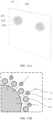
- the conductive plating layer 131 is arranged at a local region of the second surface 13b of the mounting bracket 13, and two (referring to FIG. 8 ) or more conductive plating layers 131 may be arranged.
- one conductive plating layer 131 may be electrically connected to the first metal middle plate 212 of the first middle frame 20, to ground a side of the mounting bracket, and the other conductive plating layer 131 may be electrically connected to the second metal middle plate 222 of the second middle frame 20, to ground the other side of the mounting bracket.
- a shape of the conductive plating layer 131 includes but is not limited to a circular shape shown in FIG. 8 .
- the shape of the conductive plating layer 131 may further be polygonal, elliptical, or another irregular shape.
- an internal stress in a metal generated after the conductive plating layer 131 is arranged on the second surface 13b of the mounting bracket 13 is uneven, resulting in arching deformation in a region opposite to a position of the conductive plating layer 131 on the first surface 13a of the mounting bracket 13 (as shown in FIG. 7 ). Therefore, when the electronic device is in normal use, the arching deformation is not easily observed on the electronic device due to an action of the display layer 12.
- the conductive transition layer is added at the periphery of the conductive plating layer 131, or an outer edge of the conductive plating layer 131 is set to be in an uneven serrated shape, or a hole is dug on the conductive plating layer 131, so that a material internal stress generated by a metal plating layer arranged on the mounting bracket 13 is gradually reduced. In this way, a generated arch is gradually reduced to a large flat region, to reduce the impression degree.
- a region opposite to the conductive plating layer 131 on the first surface 13a of the mounting bracket 13 is thinned to form a recessed region, and the recessed region may compensate for arching deformation, to improve flatness of a surface opposite to the conductive plating layer 131 on the mounting bracket 13, and avoid an impression when the electronic device is exposed to light.
- the large flat region specifically refers to a plane region on the first surface of the mounting bracket except an arching deformation region.
- a conductive plating layer 131 is arranged in a partial region of a second surface 13b of a mounting bracket 13, and a conductive transition layer is arranged at an outer periphery of the conductive plating layer 131.
- the conductive transition layer includes a plurality of first sub-transition layers 132, and the plurality of first sub-transition layers 132 are spaced apart around the outer periphery of the conductive plating layer 131 for one or more turns.
- the plurality of first sub-transition layers 132 are spaced apart around the outer periphery of the conductive plating layer 131 for one turn.
- the plurality of first sub-transition layers 132 are spaced apart around the outer periphery of the conductive plating layer 131 for a plurality of turns.
- the conductive plating layer 131 is electrically connected to a middle frame 20 to ground the mounting bracket 13.
- the conductive transition layer may further be electrically connected to the middle frame 20 to ground the mounting bracket 13, or both the conductive plating layer 131 and the conductive transition layer may be electrically connected to the middle frame 20, to implement a function of grounding a plurality of positions of the mounting bracket 13.
- the plurality of first sub-transition layers 132 are spaced apart from an outer edge of the conductive plating layer 131.
- the plurality of first sub-transition layers 132 are spaced apart from the outer edge of the conductive plating layer 131, so that the two plating layers are spaced apart from each other, to reduce an internal stress in a metal.
- an area of each of the first sub-transition layers 132 is smaller than an area of the conductive plating layer 131, thus ensuring that an internal stress of the first sub-transition layer 132 is smaller than an internal stress of the conductive plating layer 131, so that arching deformation generated by the first sub-transition layer 132 is smaller than arching deformation generated by the conductive plating layer 131.
- the plurality of first sub-transition layers 132 are arranged at an outer periphery of the conductive transition layer, and the area of each of the first sub-transition layers 132 is smaller than the area of the conductive plating layer 131.
- an internal stress at the first sub-transition layer 132 on the mounting bracket 13 is less than an internal stress at a position of the conductive plating layer 131, so that the arching deformation generated by the first sub-transition layer 132 is smaller than the arching deformation generated by the conductive plating layer 131.
- a material internal stress generated on the mounting bracket 13 from the conductive plating layer 131 to the first sub-transition layer 131 is gradually reduced, and a generated arch is gradually reduced to a large flat region.
- an uneven degree occurring when the light is reflected is gradually reduced from large to small under a transition action of the first sub-transition layer 132, thereby gradually reducing an impression degree. Therefore, the impression degree is gradually weakened visually, and an impression on the electronic device is not visually obvious.
- a shape of the first sub-transition layer 132 may be circular, or as shown in FIG. 10 , the shape of the first sub-transition layer 132 may be polygonal.
- the shape of the first sub-transition layer 132 may further be elliptical, triangular, or another shape.
- the conductive transition layer further includes a plurality of second sub-transition layers 133.
- the plurality of second sub-transition layers 133 are located at an outer periphery of the plurality of first sub-transition layers 132.
- an area of the second sub-transition layer 133 is smaller than an area of the first sub-transition layer 132.
- areas of the conductive plating layer 131, the first sub-transition layer 132, and the second sub-transition layer 133 are gradually reduced, a material internal stress generated from the conductive plating layer 131, the first sub-transition layer 132 to the second sub-transition layer 133 is gradually reduced, and an arch generated on a first surface 13a of the mounting bracket 13 is gradually reduced to a large flat region, so that after the screen of the electronic device is off and is exposed to light, an uneven degree in light reflection is further gradually reduced from large to small, to gradually reduce the impression degree.
- each of the second sub-transition layers 133 is located on a centerline L between two adjacent first sub-transition layers 132. In this way, it is ensured that the arch generated on the first surface 13a of the mounting bracket 13 is uniformly and gradually reduced to a flat region, the impression on the electronic device is uniformly distributed, and the impression is not easily distributed unevenly.
- the second sub-transition layer 133 may also be arranged away from the centerline L between two adjacent first sub-transition layers 132.
- a shape of the second sub-transition layer 133 may be circular, or the shape of the second sub-transition layer 133 may also be polygonal, for example, a square as shown in FIG. 10 .
- the shape of the second sub-transition layer 133 may further be elliptical, triangular, or another shape.
- shapes of the first sub-transition layer 132 and the second sub-transition layer 133 may be the same or different.
- the first sub-transition layer 132 and the second sub-transition layer 133 at an outer periphery of the two conductive plating layers 131 may be the same or different.
- first sub-transition layer 132 and the second sub-transition layer 133 are polygons (such as triangles or polygons), because a metal plating layer of a polygon has a sharp corner, an internal stress is more obviously concentrated.
- the shapes of the first sub-transition layer 132 and the second sub-transition layer 133 are circular, the internal stress is relatively dispersed, so a generated arching deformation degree is less than an arching deformation degree caused by a polygonal metal plating layer.
- the plurality of first sub-transition layers 132 are spaced apart along an outer periphery of the conductive plating layer 131 on the outer edge of the conductive plating layer 131, for example, the plurality of first sub-transition layers 132 are adjacent to the outer edge of the conductive plating layer 131, and two adjacent first transition layers and a part of the outer edge of the conductive plating layer 131 form a notch 131a, so that the outer edge of the conductive plating layer 131 is serrated.
- the outer edge of the conductive plating layer 131 has an uneven and serrated structure, and a notch 131a is provided between the serrated structures, so that a material internal stress generated by a metal plating layer arranged on the mounting bracket 13 is reduced. In this way, a generated arch is reduced to a large flat region, to reduce the impression degree.
- the shape of the first sub-transition layer 132 may be polygonal, or as shown in FIG. 13 , the shape of the first sub-transition layer 132 may be semicircular. Certainly, in some examples, the shape of the first sub-transition layer 132 may further be polygonal, triangular, or sector-shaped. In this embodiment, shapes of the plurality of first sub-transition layers 132 may be the same or different, and shapes of the plurality of second sub-transition layers 133 may be the same or different. In the embodiment of this application, the shape of the first sub-transition layer 132 is not limited.
- the second sub-transition layers 133 may further be arranged at positions opposite the notches 131a, so that the first sub-transition layer 132 is arranged next to the outer edge of the conductive plating layer 131, and the second sub-transition layer 133 is spaced apart from the outer edge of the conductive plating layer 131.
- a difference from the foregoing embodiment is as follows:
- a plurality of openings 134 are provided on a conductive plating layer 131, and a hole bottom of the opening 134 extends to a second surface 13b of a mounting bracket 13.
- the conductive plating layer 131 is a non-connected plating layer
- the opening 134 is provided on the conductive plating layer 131
- the opening 134 is provided to release a material internal stress generated by the conductive plating layer 131, thereby reducing a stress of the conductive plating layer 131.
- a generated arch is gradually reduced to a large flat region, to reduce an impression degree.
- the plurality of openings 134 are spaced apart around a center of the conductive plating layer 131 for one or more turns.
- the plurality of openings 134 are spaced apart around the center of the conductive plating layer 131 for one turn.
- the plurality of openings 134 may be close to an outer edge of the conductive plating layer 131, which facilitates reduction of an internal stress of the conductive plating layer 131.
- the plurality of openings 134 may further be located at any position between the center and the outer edge of the conductive plating layer 131.
- the opening 134 may be a round hole, or the opening 134 may also be a square hole or an elliptical hole. In the embodiment of this application, a shape of the opening 134 is not limited.
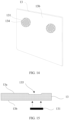
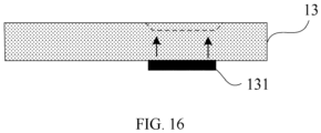
- a recessed region 135 is provided on a first surface 13a of a mounting bracket 13, and a conductive plating layer 131 is arranged at a position opposite to the recessed region 135 on a second surface 13b of the mounting bracket 13.
- the recessed region 135 on the first surface 13a of the mounting bracket 13 is arched and deformed, to compensate for arching deformation through the recessed region 135.
- no arching deformation occurs on the first surface 13a of the mounting bracket 13, and flatness of the first surface 13a of the mounting bracket 13 is improved, thereby avoiding occurrence of an impression when an electronic device is exposed to light.
- the recessed region 135 is formed on a region opposite to the conductive plating layer 131 on the first surface 13a of the mounting bracket 13, and the recessed region 135 may compensate for the arching deformation, to improve flatness of a surface opposite to the conductive plating layer 131 on the mounting bracket 13 and avoid an impression when the electronic device is exposed to light.
- a position opposite to conductive plating on the first surface 13a of the mounting bracket 13 may be thinned by performing thinning processing, such as etching, on the first surface 13a of the mounting bracket 13. It needs to be noted that, a depth of the recessed region 135 is specifically set based on a height of the arching deformation in FIG. 7 .
- a forward projection of the recessed region 135 toward the conductive plating layer 131 completely coincides with the conductive plating layer 131, ensuring that arching deformation caused by the conductive plating layer 131 can be compensated in the recessed region 135 and that arching deformation does not occur on the first surface 13a of the mounting bracket 13 when the conductive plating layer 131 is arranged on the second surface 13b of the mounting bracket 13.
- the technical solution provided in this application is described by using a foldable mobile phone as an example.
- the technical solution provided in this application is also applicable to a non-foldable mobile phone.
- the solution provided in this application is also applicable to a bar phone.
- the solution when the solution is adopted in the bar phone, because the mounting bracket 13 is made of a thin material such as an alloy or a stainless steel, a thickness of the display module 10 may be reduced, to reduce a thickness of the bar phone, or to save space in the bar phone for arranging another device.
Landscapes
- Engineering & Computer Science (AREA)
- Physics & Mathematics (AREA)
- Computer Hardware Design (AREA)
- Theoretical Computer Science (AREA)
- General Physics & Mathematics (AREA)
- Nonlinear Science (AREA)
- General Engineering & Computer Science (AREA)
- Human Computer Interaction (AREA)
- Microelectronics & Electronic Packaging (AREA)
- Signal Processing (AREA)
- Mathematical Physics (AREA)
- Chemical & Material Sciences (AREA)
- Crystallography & Structural Chemistry (AREA)
- Optics & Photonics (AREA)
- Power Engineering (AREA)
- Electromagnetism (AREA)
- Telephone Set Structure (AREA)
Abstract
Description
- This application claims priority to
Chinese Patent Application No. 202110379755.7, filed with the China National Intellectual Property Administration on April 8, 2021 - Embodiments of this application relate to the field of display technologies, and in particular, to an electronic device.
- With the continuous development of display module technology of mobile terminal devices such as a mobile phone, development of a light and thin display module has become a development trend of the display module technology. However, with the development of the light and thin display module, requirements for a display module are getting higher and higher.
- Currently, a mobile phone mainly includes a display module, a middle frame, and a battery cover. The display module and the battery cover are respectively arranged on two sides of the middle frame. The display module mainly includes a cover, a display layer, and a mounting bracket (Mounting Bracket). The display layer is located between the cover and the mounting bracket, and the mounting bracket is often made of metal materials to improve supporting performance and impact resistance of a back surface thereof. To reduce a risk of signal interference and electro-static discharge (Electro-Static discharge, ESD), the display module is often electrically connected to the middle frame through the mounting bracket to achieve grounding.
- However, to increase electrical conductivity between the mounting bracket and the middle frame, it is usually necessary to plate conductive materials on a side of the mounting bracket facing away from the display layer to improve the conductivity. However, after plating the conductive materials on the mounting bracket, a side of the mounting bracket facing the display layer and a position corresponding to the conductive materials are deformed, resulting in uneven reflected light on a deformed region under light exposure after a screen of the mobile phone is off, and observable impressions on appearance of the mobile phone, which affects the appearance of the mobile phone.
- Embodiments of this application provide an electronic device, which improves flatness of a back surface of an electroplating position of a mounting bracket in the electronic device, reduces or avoids uneven light in an electroplating region after a screen of the electronic device is off, and ensures that an impression degree of the electroplating region is reduced or there is no impression when the electronic device is exposed to light.
- According to a first aspect of the embodiments of this application, an electronic device is provided. The electronic device includes: a display module, a middle frame, and a battery cover, where the display module and the battery cover are respectively located at two sides of the middle frame;
- the display module includes at least a display layer and a mounting bracket, the mounting bracket includes a first surface and a second surface, the first surface faces the display layer, and the second surface faces the middle frame;
- a conductive plating layer is arranged on a partial region of the second surface of the mounting bracket, and a conductive transition layer is arranged at an outer periphery of the conductive plating layer; and
- the conductive plating layer is electrically connected to the middle frame.
- The conductive transition layer is added at the periphery of the conductive plating layer, or an outer edge of the conductive plating layer is set to be in an uneven serrated shape, so that a material internal stress generated by a metal plating layer arranged on the mounting bracket gradually reduces from the conductive plating layer to the conductive transition layer. In this way, an arch generated on the first surface of the mounting bracket is gradually reduced to a large flat region, to reduce the impression degree.
- In a possible implementation, the conductive transition layer includes a plurality of first sub-transition layers, and the plurality of first sub-transition layers are spaced apart around the outer periphery of the conductive plating layer for one or more turns; and
an area of each of the first sub-transition layers is smaller than an area of the conductive plating layer. - In a possible implementation, the plurality of first sub-transition layers and an outer edge of the conductive plating layer are spaced apart.
- In a possible implementation, the conductive transition layer further includes a plurality of second sub-transition layers; and
the plurality of second sub-transition layers are located at an outer periphery of the plurality of first sub-transition layers. - In a possible implementation, an area of the second sub-transition layer is smaller than an area of the first sub-transition layer.
- In a possible implementation, each of the second sub-transition layers is located on a centerline between two adjacent first sub-transition layers.
- In a possible implementation, shapes of the first sub-transition layer and the second sub-transition layer are any one of a circle, a polygon, or an ellipse.
- In a possible implementation, the plurality of first sub-transition layers are spaced apart along the outer periphery of the conductive plating layer on the outer edge of the conductive plating layer; and
two adjacent first transition layers and a part of the outer edge of the conductive plating layer form a notch, so that the outer edge of the conductive plating layer is serrated. - In a possible implementation, a shape of the first sub-transition layer is a semicircle or a polygon.
- According to a second aspect of the embodiments of this application, an electronic device is provided. The electronic device includes: a display module, a middle frame, and a battery cover, where the display module and the battery cover are respectively located at two sides of the middle frame;
- the display module includes at least a display layer and a mounting bracket, the mounting bracket includes a first surface and a second surface, the first surface faces the display layer, and the second surface faces the middle frame;
- a conductive plating layer is arranged on a partial region of the second surface of the mounting bracket, a plurality of openings are provided on the conductive plating layer, and hole bottoms of the openings extend to the second surface; and
- the conductive plating layer is electrically connected to the middle frame.
- A hole is dug on the conductive plating layer, so that an internal stress generated on the conductive plating layer is released at the opening, a material internal stress generated by a metal plating layer arranged on the mounting bracket is reduced, and an arch generated on the first surface of the mounting bracket is reduced to a large flat region, to reduce the impression degree.
- In a possible implementation, the plurality of openings are spaced apart around a center of the conductive plating layer for one or more turns.
- In a possible implementation, the opening is a round hole, a square hole, or an elliptical hole.
- According to a third aspect of the embodiments of this application, an electronic device is provided. The electronic device includes: a display module, a middle frame, and a battery cover, where the display module and the battery cover are respectively located at two sides of the middle frame;
- the display module includes at least a display layer and a mounting bracket, the mounting bracket includes a first surface and a second surface, the first surface faces the display layer, and the second surface faces the middle frame;
- a recessed region is provided on the first surface of the mounting bracket, and a conductive plating layer is arranged at a position opposite to the recessed region on the second surface of the mounting bracket; and
- the conductive plating layer is electrically connected to the middle frame.
- A region opposite to the conductive plating layer on the first surface of the mounting bracket is thinned to form a recessed region, and the recessed region may compensate for arching deformation, to improve flatness of a surface opposite to the conductive plating layer on the mounting bracket, and avoid an impression when the electronic device is exposed to light.
- In a possible implementation, an orthographic projection of the recessed region toward the conductive plating layer completely coincides with the conductive plating layer.
- In a possible implementation, a conductive member, where an end of the conductive member is electrically connected to the conductive plating layer, and another end of the conductive member is electrically connected to a metal middle plate of the middle frame.
- In a possible implementation, the conductive member is a conductive elastomer or a conductive foam.
- In a possible implementation, the electronic device is a foldable device.
- In a possible implementation, the mounting bracket is a conductive mounting bracket made of metal alloy or stainless steel.
- In a possible implementation, a thickness of the conductive plating layer is less than or equal to 0.2 mm.
- According to a fourth aspect of the embodiments of this application, a display module is provided, and is applied to an electronic device. The display module includes at least a display layer and a mounting bracket, where the mounting bracket includes a first surface and a second surface arranged opposite to the first surface, and the first surface faces the display layer;
- a conductive plating layer is arranged on a partial region of the second surface of the mounting bracket, and a conductive transition layer is arranged at an outer periphery of the conductive plating layer; and
- the conductive plating layer is configured to be electrically connected to a middle frame of the electronic device.
- According to a fifth aspect of the embodiments of this application, a display module is provided, and is applied to an electronic device. The display module includes at least a display layer and a mounting bracket, where the mounting bracket includes a first surface and a second surface arranged opposite to the first surface, and the first surface faces the display layer;
- a conductive plating layer is arranged on a partial region of the second surface of the mounting bracket, a plurality of openings are provided on the conductive plating layer, and hole bottoms of the openings extend to the second surface; and
- the conductive plating layer is configured to be electrically connected to a middle frame of the electronic device.
- According to a sixth aspect of the embodiments of this application, a display module is provided, and is applied to an electronic device. The display module includes at least a display layer and a mounting bracket, where the mounting bracket includes a first surface and a second surface arranged opposite to the first surface, and the first surface faces the display layer;
- a recessed region is provided on the first surface of the mounting bracket, and a conductive plating layer is arranged at a position opposite to the recessed region on the second surface of the mounting bracket; and
- the conductive plating layer is configured to be electrically connected to a middle frame of the electronic device.
-
-
FIG. 1 is a schematic diagram of a three-dimensional structure of an electronic device in an unfolded state according to an embodiment of this application; -
FIG. 2 is a schematic diagram of an electronic device in a semi-folded state according to an embodiment of this application; -
FIG. 3 is a schematic diagram of an electronic device in a folded state according to an embodiment of this application; -
FIG. 4 is an exploded schematic diagram of an electronic device according to an embodiment of this application; -
FIG. 5 is a schematic structural diagram of a display module in an electronic device according to an embodiment of this application; -
FIG. 6 is a schematic cross-sectional structural diagram of an electronic device along an A-A direction ofFIG. 1 according to an embodiment of this application; -
FIG. 7 is a schematic cross-sectional structural diagram of a mounting bracket in an electronic device; -
FIG. 8 is a schematic diagram of a three-dimensional structure of a mounting bracket and a conductive plating layer in an electronic device; -
FIG. 9 is a schematic diagram of a three-dimensional structure of a mounting bracket and a conductive plating layer of an electronic device according to an embodiment of this application; -
FIG. 10 is a schematic diagram of a three-dimensional structure of a mounting bracket and a conductive plating layer of an electronic device according to an embodiment of this application; -
FIG. 11A is a schematic diagram of a three-dimensional structure of a mounting bracket and a conductive plating layer of an electronic device according to an embodiment of this application; -
FIG. 11B is an enlarged schematic view of a dashed box inFIG. 11A ; -
FIG. 12 is a schematic diagram of a three-dimensional structure of a mounting bracket and a conductive plating layer of an electronic device according to an embodiment of this application; -
FIG. 13 is a schematic diagram of a three-dimensional structure of a mounting bracket and a conductive plating layer of an electronic device according to an embodiment of this application; -
FIG. 14 is a schematic diagram of a three-dimensional structure of a mounting bracket and a conductive plating layer of an electronic device according to an embodiment of this application; -
FIG. 15 is a schematic diagram of a split structure of a mounting bracket and a conductive plating layer of an electronic device according to an embodiment of this application; and -
FIG. 16 is a schematic diagram of a split structure of a mounting bracket and a conductive plating layer of an electronic device according to an embodiment of this application. - Brief description of reference numerals of the accompanying drawings:
- 100-electronic device; 10-display module; 10a-first portion; 10b-second portion;
- 10c-third portion; 11-cover; 12-display layer; 13-mounting bracket;
- 131-conductive plating layer; 13a-first surface; 13b-second surface; 132-first sub-transition layer;
- 133-second sub-transition layer; 134-opening; 135-recessed region; 20-middle frame;
- 21-first middle frame; 211-first frame; 212-first metal middle plate;
- 22-second middle frame; 221-second frame; 222-second metal middle plate; 23-rotary connector;
- 30-front cover; 40-battery cover; 50-circuit board; 60-battery; and 70-conductive member.
- Terms used in implementations of this application are merely intended to explain specific embodiments of this application rather than limit this application. The following describes implementations of the embodiments of this application in detail with reference to the accompanying drawings.
- The embodiments of this application provide an electronic device. The electronic device may be, but is not limited to, a mobile terminal, a fixed terminal, or a foldable terminal having a display module such as a mobile phone, a tablet computer, a notebook computer, an ultra-mobile personal computer (ultra-mobile personal computer, UMPC), a handheld computer, an intercom, a netbook, a POS terminal, a personal digital assistant (personal digital assistant, PDA), a drive recorder, and a security device.
- In the embodiments of this application, an example in which a mobile phone is the electronic device is used for description, and specifically, a foldable mobile phone is used as an example for description. The foldable mobile phone may be an inward foldable mobile phone (that is, a display module is folded inward) or an outward foldable mobile phone (that is, a display module is folded outward). In the embodiments of this application, the inward foldable mobile phone is specifically used as an example for description.
-
FIG. 1 is a schematic diagram of a mobile phone in an unfolded state. As shown inFIG. 1 , anelectronic device 100 may include: adisplay module 10, amiddle frame 20, abattery cover 40, and afront cover 30. Thedisplay module 10 and thefront cover 30 are located at one side of themiddle frame 20, thebattery cover 40 is located at the other side of themiddle frame 20, and thefront cover 30 is connected to themiddle frame 20. - The
front cover 30 is configured to block a connection position between thedisplay module 10 and themiddle frame 20. There may be a certain gap between thefront cover 30 and a surface of thedisplay module 10, or thefront cover 30 and the surface of thedisplay module 10 may be in contact but not sealed, so that thefront cover 30 is not likely to obstruct bending of thedisplay module 10 when the mobile phone is folded. Thefront cover 30 may be an insulation front cover. - In the embodiments of this application, as shown in
FIG. 1 , themiddle frame 20 may include a firstmiddle frame 21, a secondmiddle frame 22, and arotary connector 23. The firstmiddle frame 21 and the secondmiddle frame 22 are rotated relative to therotary connector 23, for example, an end of the firstmiddle frame 21 and an end of the secondmiddle frame 22 are rotatably connected to two sides of therotary connector 23 respectively, and the other end of the firstmiddle frame 21 and the other end of the secondmiddle frame 22 are rotatable around therotary connector 23. - It needs to be noted that, to switch between a folded state and an unfolded state of the mobile phone, when the first
middle frame 20 and the secondmiddle frame 20 are rotated, thefront cover 30, thebattery cover 40, and thedisplay module 10 may all be folded or unfolded with rotation of the firstmiddle frame 20 and the secondmiddle frame 20. - For example, as shown in
FIG. 1 , when the mobile phone is in the unfolded state, the firstmiddle frame 21 and the secondmiddle frame 22 are rotated to a maximum state relative to therotary connector 23, and thefront cover 30, thebattery cover 40, and thedisplay module 10 are all in the unfolded state. When the firstmiddle frame 21 and the secondmiddle frame 22 are rotated in a direction of a dashed arrow or a solid arrow inFIG. 1 , as shown inFIG. 2 , the mobile phone may be in a semi-folded state, the firstmiddle frame 21 and the secondmiddle frame 22 are close to each other, and thefront cover 30, thebattery cover 40, and thedisplay module 10 are in a bent state.FIG. 3 is a schematic diagram of a mobile phone in a folded state. As shown inFIG. 3 , the firstmiddle frame 21 and the secondmiddle frame 22 are opposite, and thefront cover 30, thebattery cover 40, and thedisplay module 10 are all in the folded state. Therefore, in the embodiments of this application, the firstmiddle frame 20, the secondmiddle frame 20, thefront cover 30, thebattery cover 40, and thedisplay module 10 are switchable between the folded and unfolded states. - Because the
display module 10 also needs to be folded during a folding process of the mobile phone, in the embodiments of this application, thedisplay module 10 may be an organic light-emitting diode (Organic Light-Emitting Diode, OLED) display screen or another bendable flexible display screen. - The
display module 10 may be configured to display an image, a text, a video, or the like. As shown inFIG. 1 , thedisplay module 10 includes afirst portion 10a, asecond portion 10b, and athird portion 10c. Thesecond portion 10b is located between thefirst portion 10a and thethird portion 10c. Thefirst portion 10a, thesecond portion 10b, and thethird portion 10c are all located on a same side of the firstmiddle frame 21 and the secondmiddle frame 22. In addition, thefirst portion 10a is fixed to the firstmiddle frame 21. Thesecond portion 10b is fixed to therotary connector 23 between the firstmiddle frame 21 and the secondmiddle frame 22. Thethird portion 10c is fixed to the secondmiddle frame 22. When the mobile phone is folded, thesecond portion 10b is bent. - It is understandable that, when the
electronic device 100 is an inward foldable mobile phone, as shown inFIG. 1 , theelectronic device 100 is in the unfolded state, and thefirst portion 10a, thesecond portion 10b, and thethird portion 10c are at an angle of approximately 180 degrees (slight deviations are allowed, for example, 165 degrees, 177 degrees, or 185 degrees). In this case, thedisplay module 10 has a continuous display region with a large area, that is, thedisplay module 10 may achieve large screen display, making user experience better. When theelectronic device 100 is in the folded state, thedisplay module 10 is located between the firstmiddle frame 21 and the second middle frame 22 (as shown inFIG. 3 ), thesecond portion 10b is bent, and thefirst portion 10a and thethird portion 10c overlap each other. - Certainly, in some examples, the
electronic device 100 is an outward foldable mobile phone (that is, thedisplay module 10 is exposed when the electronic device is in the folded state). In this case, the firstmiddle frame 21 and the secondmiddle frame 22 are located between thefirst portion 10a and thethird portion 10c when theelectronic device 100 is in the folded state. -
FIG. 4 is an exploded schematic diagram of a mobile phone. As shown inFIG. 4 , the firstmiddle frame 21 may include: a first metalmiddle plate 212 and afirst frame 211 enclosed on an outer edge of the first metalmiddle plate 212. Thefirst frame 211 may include a side frame, a top frame, and a bottom frame. - The second
middle frame 22 may include: a second metalmiddle plate 222 and asecond frame 221 enclosed on an outer edge of the second metalmiddle plate 222. Thesecond frame 221 may include: a side frame, a top frame, and a bottom frame. Therotary connector 23 may be respectively connected to the first metalmiddle plate 212 and the second metalmiddle plate 222. - In the embodiments of this application, the
first frame 211 and thesecond frame 221 are fixedly connected to the first metalmiddle plate 212 and the second metalmiddle plate 222 through injection molding. The first metalmiddle plate 212 and the second metalmiddle plate 222 may be an aluminum plate, an aluminum alloy, or a magnesium alloy. Thefirst frame 211 and thesecond frame 221 may be metal frames, glass frames, or ceramic frames. - As shown in
FIG. 4 , theelectronic device 100 may further include acircuit board 50 and abattery 60. Thebattery 60 may be connected to a charging management module and thecircuit board 50 through a power management module. The power management module receives an input from thebattery 60 and/or an input from the charging management module, and supplies power to a processor, an internal memory, an external memory, afoldable display module 10, a camera module, a communication module, and the like. The power management module may be further configured to monitor a parameter such as a capacity of thebattery 60, a cycle count of thebattery 60, or a health state (electric leakage and impedance) of thebattery 60. In some other embodiments, the power management module may also be arranged in the processor of thecircuit board 50. In some other embodiments, the power management module and the charging management module may also be arranged in a same device. - It may be understood that the schematic structure in the embodiments of this application constitutes no specific limitation on the
electronic device 100. In some other embodiments of this application, theelectronic device 100 may include more or fewer components than those shown in the figure, or some components may be combined, or some components may be split, or different component arrangements may be used. For example, theelectronic device 100 may further include devices such as a camera (for example, a front-facing camera and a rear-facing camera) and a camera flash. - As shown in
FIG. 5 , thedisplay module 10 may include: a cover (Cover) 11, adisplay layer 12, and a mountingbracket 13. Thedisplay layer 12 is located between thecover 11 and the mountingbracket 13, and the mountingbracket 13 is configured to support thedisplay layer 12. To ensure that the mountingbracket 13 has a supporting performance, the mountingbracket 13 is often made of a metal material. However, to reduce a risk of signal interference and electro-static discharge (Electro-Static discharge, ESD) during whole machine design, it is necessary to electrically connect a suspended metal (for example, the mounting bracket 13) to themiddle frame 20 to achieve grounding. - The mounting
bracket 13 is usually electrically connected to themiddle frame 20 through aconductive member 70, and theconductive member 70 may be a conductive material such as an elastomer or a conductive foam. - The mounting
bracket 13 is generally made of a copper layer, because the copper layer has good electrical conductivity, and may achieve a good grounding performance with themiddle frame 20. However, when theelectronic device 100 is a foldable device, due to a weight requirement of a whole machine, and a requirement that the mountingbracket 13 for a foldable mobile phone should not only meet a supporting performance, but also have a bending function, a thickness of the mountingbracket 13 should be small. However, if the mountingbracket 13 continues to be made of the copper layer, when a thickness of the copper layer is small, the copper layer cannot play a good supporting role on thedisplay layer 12. Therefore, in a foldable device, the mountingbracket 13 is not suitable for being made of the copper layer. Generally, in the foldable device, the mountingbracket 13 is made of a thin material which has a good supporting performance such as an alloy material or a stainless steel. - However, when the mounting
bracket 13 is made of an alloy material (such as an aluminum alloy or a copper alloy), or a stainless steel, or the like, because the alloy material or stainless steel has weak electrical conductivity, when the mountingbracket 13 is grounded with themiddle frame 20 through theconductive member 70, to improve electrical conductivity of a surface of the mountingbracket 13, as shown inFIG. 6 andFIG. 7 , the mountingbracket 13 includes afirst surface 13a and asecond surface 13b, thefirst surface 13a faces thedisplay layer 12, thesecond surface 13b faces the first metalmiddle plate 212 and the second metalmiddle plate 222 of themiddle frame 20, a nickel/gold or another conductive material is plated at a grounding position of thesecond surface 13b of the mountingbracket 13 to form aconductive plating layer 131, and theconductive plating layer 131 may improve a conductive performance of the grounding position of the mountingbracket 13, to ensure a stable and effective electrical connection between the mountingbracket 13 and themiddle frame 20 through theconductive member 70 and theconductive plating layer 131. - As shown in
FIG. 7 and FIG. 8 , theconductive plating layer 131 is arranged at a local region of thesecond surface 13b of the mountingbracket 13, and two (referring toFIG. 8 ) or more conductive plating layers 131 may be arranged. When there are two conductive plating layers 131, as shown inFIG. 6 , oneconductive plating layer 131 may be electrically connected to the first metalmiddle plate 212 of the firstmiddle frame 20, to ground a side of the mounting bracket, and the otherconductive plating layer 131 may be electrically connected to the second metalmiddle plate 222 of the secondmiddle frame 20, to ground the other side of the mounting bracket. - It needs to be noted that, a shape of the
conductive plating layer 131 includes but is not limited to a circular shape shown inFIG. 8 . In some examples, the shape of theconductive plating layer 131 may further be polygonal, elliptical, or another irregular shape. - However, an internal stress in a metal generated after the
conductive plating layer 131 is arranged on thesecond surface 13b of the mountingbracket 13 is uneven, resulting in arching deformation in a region opposite to a position of theconductive plating layer 131 on thefirst surface 13a of the mounting bracket 13 (as shown inFIG. 7 ). Therefore, when the electronic device is in normal use, the arching deformation is not easily observed on the electronic device due to an action of thedisplay layer 12. However, when a screen of the electronic device is off and exposed to light, reflection of the arched region to the light is uneven, resulting in observable impressions on an appearance of the region, for example, an uneven impression appears on a position of thedisplay module 10 opposite to theconductive plating layer 131, thus affecting an appearance of the electronic device. - To solve the foregoing problems, in the electronic device provided in the embodiments of this application, the conductive transition layer is added at the periphery of the
conductive plating layer 131, or an outer edge of theconductive plating layer 131 is set to be in an uneven serrated shape, or a hole is dug on theconductive plating layer 131, so that a material internal stress generated by a metal plating layer arranged on the mountingbracket 13 is gradually reduced. In this way, a generated arch is gradually reduced to a large flat region, to reduce the impression degree. Alternatively, a region opposite to theconductive plating layer 131 on thefirst surface 13a of the mountingbracket 13 is thinned to form a recessed region, and the recessed region may compensate for arching deformation, to improve flatness of a surface opposite to theconductive plating layer 131 on the mountingbracket 13, and avoid an impression when the electronic device is exposed to light. - It needs to be noted that, the large flat region specifically refers to a plane region on the first surface of the mounting bracket except an arching deformation region.
- The following describes several solutions provided in the embodiments of this application in detail through several embodiments.
- In the embodiment of this application, as shown in
FIG. 9 , aconductive plating layer 131 is arranged in a partial region of asecond surface 13b of a mountingbracket 13, and a conductive transition layer is arranged at an outer periphery of theconductive plating layer 131. As shown inFIG. 9 , the conductive transition layer includes a plurality of firstsub-transition layers 132, and the plurality of firstsub-transition layers 132 are spaced apart around the outer periphery of theconductive plating layer 131 for one or more turns. For example, inFIG. 9 , the plurality of firstsub-transition layers 132 are spaced apart around the outer periphery of theconductive plating layer 131 for one turn. Certainly, in some examples, the plurality of firstsub-transition layers 132 are spaced apart around the outer periphery of theconductive plating layer 131 for a plurality of turns. - In the embodiment of this application, the
conductive plating layer 131 is electrically connected to amiddle frame 20 to ground the mountingbracket 13. Certainly, in some examples, the conductive transition layer may further be electrically connected to themiddle frame 20 to ground the mountingbracket 13, or both theconductive plating layer 131 and the conductive transition layer may be electrically connected to themiddle frame 20, to implement a function of grounding a plurality of positions of the mountingbracket 13. - In the embodiment of this application, the plurality of first
sub-transition layers 132 are spaced apart from an outer edge of theconductive plating layer 131. For example, as shown inFIG. 9 , the plurality of firstsub-transition layers 132 are spaced apart from the outer edge of theconductive plating layer 131, so that the two plating layers are spaced apart from each other, to reduce an internal stress in a metal. - It should be noted that, an area of each of the first sub-transition layers 132 is smaller than an area of the
conductive plating layer 131, thus ensuring that an internal stress of thefirst sub-transition layer 132 is smaller than an internal stress of theconductive plating layer 131, so that arching deformation generated by thefirst sub-transition layer 132 is smaller than arching deformation generated by theconductive plating layer 131. - Therefore, in the embodiment of this application, the plurality of first
sub-transition layers 132 are arranged at an outer periphery of the conductive transition layer, and the area of each of the first sub-transition layers 132 is smaller than the area of theconductive plating layer 131. In this way, an internal stress at thefirst sub-transition layer 132 on the mountingbracket 13 is less than an internal stress at a position of theconductive plating layer 131, so that the arching deformation generated by thefirst sub-transition layer 132 is smaller than the arching deformation generated by theconductive plating layer 131. Therefore, in the embodiment of this application, a material internal stress generated on the mountingbracket 13 from theconductive plating layer 131 to thefirst sub-transition layer 131 is gradually reduced, and a generated arch is gradually reduced to a large flat region. In this way, after a screen of an electronic device is off and is exposed to light, an uneven degree occurring when the light is reflected is gradually reduced from large to small under a transition action of thefirst sub-transition layer 132, thereby gradually reducing an impression degree. Therefore, the impression degree is gradually weakened visually, and an impression on the electronic device is not visually obvious. - In the embodiment of this application, as shown in
FIG. 9 , a shape of thefirst sub-transition layer 132 may be circular, or as shown inFIG. 10 , the shape of thefirst sub-transition layer 132 may be polygonal. - Certainly, in some examples, the shape of the
first sub-transition layer 132 may further be elliptical, triangular, or another shape. - In a possible implementation, as shown in
FIG. 11A , the conductive transition layer further includes a plurality of second sub-transition layers 133. The plurality of secondsub-transition layers 133 are located at an outer periphery of the plurality of first sub-transition layers 132. - As shown in
FIG. 11A , an area of thesecond sub-transition layer 133 is smaller than an area of thefirst sub-transition layer 132. Thus, areas of theconductive plating layer 131, thefirst sub-transition layer 132, and thesecond sub-transition layer 133 are gradually reduced, a material internal stress generated from theconductive plating layer 131, thefirst sub-transition layer 132 to thesecond sub-transition layer 133 is gradually reduced, and an arch generated on afirst surface 13a of the mountingbracket 13 is gradually reduced to a large flat region, so that after the screen of the electronic device is off and is exposed to light, an uneven degree in light reflection is further gradually reduced from large to small, to gradually reduce the impression degree. - In the embodiment of this application, when the plurality of second
sub-transition layers 133 are distributed at the outer periphery of the plurality of firstsub-transition layers 132, as shown inFIG. 11B , each of the second sub-transition layers 133 is located on a centerline L between two adjacent first sub-transition layers 132. In this way, it is ensured that the arch generated on thefirst surface 13a of the mountingbracket 13 is uniformly and gradually reduced to a flat region, the impression on the electronic device is uniformly distributed, and the impression is not easily distributed unevenly. - Certainly, in some examples, the
second sub-transition layer 133 may also be arranged away from the centerline L between two adjacent first sub-transition layers 132. - In the embodiment of this application, as shown in
FIG. 11A , a shape of thesecond sub-transition layer 133 may be circular, or the shape of thesecond sub-transition layer 133 may also be polygonal, for example, a square as shown inFIG. 10 . - Certainly, in some examples, the shape of the
second sub-transition layer 133 may further be elliptical, triangular, or another shape. - It needs to be noted that, shapes of the
first sub-transition layer 132 and thesecond sub-transition layer 133 may be the same or different. When two conductive plating layers 131 are arranged on thefirst surface 13a of the mountingbracket 13, thefirst sub-transition layer 132 and thesecond sub-transition layer 133 at an outer periphery of the two conductive plating layers 131 may be the same or different. - It should be noted that, when the shapes of the
first sub-transition layer 132 and thesecond sub-transition layer 133 are polygons (such as triangles or polygons), because a metal plating layer of a polygon has a sharp corner, an internal stress is more obviously concentrated. When the shapes of thefirst sub-transition layer 132 and thesecond sub-transition layer 133 are circular, the internal stress is relatively dispersed, so a generated arching deformation degree is less than an arching deformation degree caused by a polygonal metal plating layer. - In a possible implementation, as shown in
FIG. 12 , the plurality of firstsub-transition layers 132 are spaced apart along an outer periphery of theconductive plating layer 131 on the outer edge of theconductive plating layer 131, for example, the plurality of firstsub-transition layers 132 are adjacent to the outer edge of theconductive plating layer 131, and two adjacent first transition layers and a part of the outer edge of theconductive plating layer 131 form anotch 131a, so that the outer edge of theconductive plating layer 131 is serrated. In this way, the outer edge of theconductive plating layer 131 has an uneven and serrated structure, and anotch 131a is provided between the serrated structures, so that a material internal stress generated by a metal plating layer arranged on the mountingbracket 13 is reduced. In this way, a generated arch is reduced to a large flat region, to reduce the impression degree. - In the embodiment of this application, as shown in
FIG. 12 , the shape of thefirst sub-transition layer 132 may be polygonal, or as shown inFIG. 13 , the shape of thefirst sub-transition layer 132 may be semicircular. Certainly, in some examples, the shape of thefirst sub-transition layer 132 may further be polygonal, triangular, or sector-shaped. In this embodiment, shapes of the plurality of firstsub-transition layers 132 may be the same or different, and shapes of the plurality of secondsub-transition layers 133 may be the same or different. In the embodiment of this application, the shape of thefirst sub-transition layer 132 is not limited. - It needs to be noted that, in
FIG. 11A andFIG. 12 , the second sub-transition layers 133 may further be arranged at positions opposite thenotches 131a, so that thefirst sub-transition layer 132 is arranged next to the outer edge of theconductive plating layer 131, and thesecond sub-transition layer 133 is spaced apart from the outer edge of theconductive plating layer 131. - A difference from the foregoing embodiment is as follows: In this embodiment, as shown in
FIG. 14 , a plurality ofopenings 134 are provided on aconductive plating layer 131, and a hole bottom of theopening 134 extends to asecond surface 13b of a mountingbracket 13. Thus, theconductive plating layer 131 is a non-connected plating layer, theopening 134 is provided on theconductive plating layer 131, and theopening 134 is provided to release a material internal stress generated by theconductive plating layer 131, thereby reducing a stress of theconductive plating layer 131. In this way, a generated arch is gradually reduced to a large flat region, to reduce an impression degree. - In the embodiment of this application, the plurality of
openings 134 are spaced apart around a center of theconductive plating layer 131 for one or more turns. For example, as shown inFIG. 14 , the plurality ofopenings 134 are spaced apart around the center of theconductive plating layer 131 for one turn. The plurality ofopenings 134 may be close to an outer edge of theconductive plating layer 131, which facilitates reduction of an internal stress of theconductive plating layer 131. Certainly, in some examples, the plurality ofopenings 134 may further be located at any position between the center and the outer edge of theconductive plating layer 131. - In the embodiment of this application, as shown in
FIG. 14 , theopening 134 may be a round hole, or theopening 134 may also be a square hole or an elliptical hole. In the embodiment of this application, a shape of theopening 134 is not limited. - In the embodiment of this application, as shown in
FIG. 15 , a recessedregion 135 is provided on afirst surface 13a of a mountingbracket 13, and aconductive plating layer 131 is arranged at a position opposite to the recessedregion 135 on asecond surface 13b of the mountingbracket 13. Thus, when an internal stress is generated in theconductive plating layer 131 on thesecond surface 13b of the mountingbracket 13, the recessedregion 135 on thefirst surface 13a of the mountingbracket 13 is arched and deformed, to compensate for arching deformation through the recessedregion 135. In this way, as shown inFIG. 16 , no arching deformation occurs on thefirst surface 13a of the mountingbracket 13, and flatness of thefirst surface 13a of the mountingbracket 13 is improved, thereby avoiding occurrence of an impression when an electronic device is exposed to light. - Therefore, in the electronic device provided in the embodiment of this application, the recessed
region 135 is formed on a region opposite to theconductive plating layer 131 on thefirst surface 13a of the mountingbracket 13, and the recessedregion 135 may compensate for the arching deformation, to improve flatness of a surface opposite to theconductive plating layer 131 on the mountingbracket 13 and avoid an impression when the electronic device is exposed to light. - In the embodiment of this application, when the recessed
region 135 is formed on thefirst surface 13a of the mountingbracket 13, specifically, a position opposite to conductive plating on thefirst surface 13a of the mountingbracket 13 may be thinned by performing thinning processing, such as etching, on thefirst surface 13a of the mountingbracket 13. It needs to be noted that, a depth of the recessedregion 135 is specifically set based on a height of the arching deformation inFIG. 7 . - In a possible implementation, a forward projection of the recessed
region 135 toward theconductive plating layer 131 completely coincides with theconductive plating layer 131, ensuring that arching deformation caused by theconductive plating layer 131 can be compensated in the recessedregion 135 and that arching deformation does not occur on thefirst surface 13a of the mountingbracket 13 when theconductive plating layer 131 is arranged on thesecond surface 13b of the mountingbracket 13. - It needs to be noted that, the technical solution provided in this application is described by using a foldable mobile phone as an example. In some examples, the technical solution provided in this application is also applicable to a non-foldable mobile phone. For example, the solution provided in this application is also applicable to a bar phone. In this case, when the solution is adopted in the bar phone, because the mounting
bracket 13 is made of a thin material such as an alloy or a stainless steel, a thickness of thedisplay module 10 may be reduced, to reduce a thickness of the bar phone, or to save space in the bar phone for arranging another device. - In the descriptions of the embodiments of this application, it should be noted that, unless expressly stated and defined otherwise, the terms "mounting", "connected", "connection", or the like are to be construed broadly, for example, as a fixed connection, an indirect connection through an intermediary, or internal communication between two elements or mutual interaction relationship between two elements. A person of ordinary skill in the art may understand the specific meanings of the foregoing terms in the embodiments of this application according to specific situations.
- In the embodiments of this application, it is implied that an apparatus or element in question needs to have a particular orientation, or needs to be constructed and operated in a particular orientation, and therefore cannot be construed as a limitation on the embodiments of this application. In the description of the embodiments of this application, unless otherwise exactly and specifically ruled, "a plurality of" means two or more than two.
- In the specification of the embodiments of this application, claims, and accompanying drawings, the terms "first", "second", "third", "fourth", and so on (if existing) are intended to distinguish between similar objects but do not necessarily indicate a specific order or sequence. It is to be understood that data used in this way is interchangeable in a suitable case, so that the embodiments of the embodiments of this application described herein can be implemented in a sequence in addition to the sequence shown or described herein. Furthermore, the terms "may include" and "have" and any variation thereof are intended to cover non-exclusive inclusion. For example, processes, methods, systems, products, or devices including a series of steps or units are not necessarily limited to those steps or units expressly listed, and instead, may include other steps or units not expressly listed or inherent to these processes, methods, products, or devices.
- Finally, it should be noted that: the foregoing embodiments are merely intended for describing the technical solutions of the embodiments of this application other than limiting this application. Although the embodiments of this application are described in detail with reference to the foregoing embodiments, a person of ordinary skill in the art should understand that: modifications may still be made to the technical solutions in the foregoing embodiments, or equivalent replacements may be made to some of or all the technical features; and such modifications or replacements will not cause the essence of corresponding technical solutions to depart from the scope of the technical solutions in the embodiments of the embodiments of this application.
Claims (19)
- An electronic device, comprising: a display module, a middle frame, and a battery cover, wherein the display module and the battery cover are respectively located at two sides of the middle frame;the display module comprises at least a display layer and a mounting bracket, the mounting bracket comprises a first surface and a second surface, the first surface faces the display layer, and the second surface faces the middle frame;a conductive plating layer is arranged on a partial region of the second surface of the mounting bracket, and a conductive transition layer is arranged at an outer periphery of the conductive plating layer; andthe conductive plating layer is electrically connected to the middle frame.
- The electronic device according to claim 1, wherein the conductive transition layer comprises a plurality of first sub-transition layers, and the plurality of first sub-transition layers are spaced apart around the outer periphery of the conductive plating layer for one or more turns; and
an area of each of the first sub-transition layers is smaller than an area of the conductive plating layer. - The electronic device according to claim 2, wherein the plurality of first sub-transition layers and an outer edge of the conductive plating layer are spaced apart.
- The electronic device according to claim 2 or 3, wherein the conductive transition layer further comprises a plurality of second sub-transition layers; and
the plurality of second sub-transition layers are located at an outer periphery of the plurality of first sub-transition layers. - The electronic device according to claim 4, wherein an area of the second sub-transition layer is smaller than an area of the first sub-transition layer.
- The electronic device according to claim 4 or 5, wherein each of the second sub-transition layers is located on a centerline between two adjacent first sub-transition layers.
- The electronic device according to any one of claims 4 to 6, wherein shapes of the first sub-transition layer and the second sub-transition layer are any one of a circle, a polygon, or an ellipse.
- The electronic device according to claim 2, wherein the plurality of first sub-transition layers are spaced apart along the outer periphery of the conductive plating layer on the outer edge of the conductive plating layer; and
two adjacent first transition layers and a part of the outer edge of the conductive plating layer form a notch, so that the outer edge of the conductive plating layer is serrated. - The electronic device according to claim 8, wherein a shape of the first sub-transition layer is a semicircle or a polygon.
- An electronic device, comprising: a display module, a middle frame, and a battery cover, wherein the display module and the battery cover are respectively located at two sides of the middle frame;the display module comprises at least a display layer and a mounting bracket, the mounting bracket comprises a first surface and a second surface, the first surface faces the display layer, and the second surface faces the middle frame;a conductive plating layer is arranged on a partial region of the second surface of the mounting bracket, a plurality of openings are provided on the conductive plating layer, and hole bottoms of the openings extend to the second surface; andthe conductive plating layer is electrically connected to the middle frame.
- The electronic device according to claim 10, wherein the plurality of openings are spaced apart around a center of the conductive plating layer for one or more turns.
- The electronic device according to claim 11, wherein the opening is a round hole, a square hole, or an elliptical hole.
- An electronic device, comprising: a display module, a middle frame, and a battery cover, wherein the display module and the battery cover are respectively located at two sides of the middle frame;the display module comprises at least a display layer and a mounting bracket, the mounting bracket comprises a first surface and a second surface, the first surface faces the display layer, and the second surface faces the middle frame;a recessed region is provided on the first surface of the mounting bracket, and a conductive plating layer is arranged at a position opposite to the recessed region on the second surface of the mounting bracket; andthe conductive plating layer is electrically connected to the middle frame.
- The electronic device according to claim 13, wherein an orthographic projection of the recessed region toward the conductive plating layer completely coincides with the conductive plating layer.
- The electronic device according to any one of claims 1 to 14, further comprising: a conductive member, wherein an end of the conductive member is electrically connected to the conductive plating layer, and another end of the conductive member is electrically connected to a metal middle plate of the middle frame.
- The electronic device according to claim 15, wherein the conductive member is a conductive elastomer or a conductive foam.
- The electronic device according to any one of claims 1 to 16, wherein the electronic device is a foldable device.
- The electronic device according to any one of claims 1 to 17, wherein the mounting bracket is a conductive mounting bracket made of metal alloy or stainless steel.
- The electronic device according to any one of claims 1 to 17, wherein a thickness of the conductive plating layer is less than or equal to 0.2 mm.
Applications Claiming Priority (2)
| Application Number | Priority Date | Filing Date | Title |
|---|---|---|---|
| CN202110379755.7A CN113286456B (en) | 2021-04-08 | 2021-04-08 | Electronic equipment |
| PCT/CN2022/074996 WO2022213715A1 (en) | 2021-04-08 | 2022-01-29 | Electronic device |
Publications (3)
| Publication Number | Publication Date |
|---|---|
| EP4187887A1 true EP4187887A1 (en) | 2023-05-31 |
| EP4187887A4 EP4187887A4 (en) | 2024-02-21 |
| EP4187887B1 EP4187887B1 (en) | 2024-12-04 |
Family
ID=77276389
Family Applications (1)
| Application Number | Title | Priority Date | Filing Date |
|---|---|---|---|
| EP22783786.1A Active EP4187887B1 (en) | 2021-04-08 | 2022-01-29 | Electronic device |
Country Status (4)
| Country | Link |
|---|---|
| US (1) | US12225144B2 (en) |
| EP (1) | EP4187887B1 (en) |
| CN (1) | CN113286456B (en) |
| WO (1) | WO2022213715A1 (en) |
Families Citing this family (3)
| Publication number | Priority date | Publication date | Assignee | Title |
|---|---|---|---|---|
| CN113286456B (en) | 2021-04-08 | 2025-05-27 | 荣耀终端股份有限公司 | Electronic equipment |
| CN115019636B (en) * | 2021-10-26 | 2023-08-15 | 荣耀终端有限公司 | Flexible display module and electronic equipment |
| CN118116281A (en) * | 2022-11-30 | 2024-05-31 | 华为技术有限公司 | Folding display terminal |
Family Cites Families (13)
| Publication number | Priority date | Publication date | Assignee | Title |
|---|---|---|---|---|
| JPH0745982A (en) * | 1993-07-28 | 1995-02-14 | Toshiba Corp | Connection structure between shield case and printed wiring board |
| CN204376971U (en) * | 2015-01-08 | 2015-06-03 | 联想(北京)有限公司 | Electronic equipment |
| KR101659476B1 (en) | 2016-01-04 | 2016-09-23 | (주)멜파스 | 3 dimension touch screen panel |
| KR102494409B1 (en) * | 2018-07-10 | 2023-02-01 | 삼성디스플레이 주식회사 | Display device |
| KR102600040B1 (en) | 2018-08-03 | 2023-11-08 | 삼성디스플레이 주식회사 | Display device |
| CN208820830U (en) | 2018-10-19 | 2019-05-03 | Oppo广东移动通信有限公司 | electronic device |
| KR102637071B1 (en) * | 2018-11-16 | 2024-02-16 | 삼성디스플레이 주식회사 | Display device and electronic device having the same |
| KR102880919B1 (en) * | 2019-08-06 | 2025-11-05 | 삼성전자 주식회사 | Electronic device including fpcb structure |
| CN111782078B (en) | 2020-06-19 | 2023-12-22 | 维沃移动通信有限公司 | Conductive foam and electronic equipment |
| CN212302932U (en) | 2020-08-21 | 2021-01-05 | 北京小米移动软件有限公司 | Display panels and electronic equipment |
| CN212516364U (en) | 2020-08-21 | 2021-02-09 | 北京小米移动软件有限公司 | Flexible Display Panels and Electronic Devices |
| CN215417305U (en) * | 2021-04-08 | 2022-01-04 | 荣耀终端有限公司 | Display module assembly and electronic equipment |
| CN113286456B (en) | 2021-04-08 | 2025-05-27 | 荣耀终端股份有限公司 | Electronic equipment |
-
2021
- 2021-04-08 CN CN202110379755.7A patent/CN113286456B/en active Active
-
2022
- 2022-01-29 US US18/022,373 patent/US12225144B2/en active Active
- 2022-01-29 WO PCT/CN2022/074996 patent/WO2022213715A1/en not_active Ceased
- 2022-01-29 EP EP22783786.1A patent/EP4187887B1/en active Active
Also Published As
| Publication number | Publication date |
|---|---|
| CN113286456A (en) | 2021-08-20 |
| US20230319171A1 (en) | 2023-10-05 |
| EP4187887A4 (en) | 2024-02-21 |
| EP4187887B1 (en) | 2024-12-04 |
| CN113286456B (en) | 2025-05-27 |
| US12225144B2 (en) | 2025-02-11 |
| WO2022213715A1 (en) | 2022-10-13 |
Similar Documents
| Publication | Publication Date | Title |
|---|---|---|
| US12225144B2 (en) | Electronic device | |
| CN205177993U (en) | Antenna device and electronic device | |
| CN109167151B (en) | Electronic equipment | |
| CN109545085B (en) | Display panels and display devices | |
| US12401735B2 (en) | Electronic device | |
| EP3205187B1 (en) | Signal trace patterns for flexible substrates | |
| US8174452B2 (en) | Cavity antenna for wireless electronic devices | |
| TW202213298A (en) | Display module | |
| CN106940605B (en) | Display panel | |
| CN113540788B (en) | Electronic device | |
| JP2020099004A (en) | Electronic apparatus | |
| CN215417305U (en) | Display module assembly and electronic equipment | |
| US11573666B2 (en) | Display device with touch control wiring liens having hole patterns and method of manufacturing thereof | |
| CN108539369B (en) | Antenna assembly, manufacturing method of antenna assembly and electronic equipment | |
| CN217562183U (en) | Folding display terminal | |
| CN104347927B (en) | Antenna and hand-hold communication appliance | |
| CN112817471B (en) | Flexible screen, terminal equipment and manufacturing method of flexible screen | |
| EP4207953A1 (en) | Circuit board assembly and electronic device | |
| CN107623984A (en) | Flexible circuit board, manufacturing method thereof, and electronic device | |
| CN116435787B (en) | Electronic components and electronic devices | |
| CN112670322B (en) | Display devices and electronic equipment | |
| WO2018137303A1 (en) | Mobile terminal | |
| WO2024040913A1 (en) | Camera module and electronic device | |
| CN216562316U (en) | Display screen assembly and terminal equipment thereof | |
| CN111262046B (en) | Antenna circuit and mobile terminal |
Legal Events
| Date | Code | Title | Description |
|---|---|---|---|
| STAA | Information on the status of an ep patent application or granted ep patent |
Free format text: STATUS: THE INTERNATIONAL PUBLICATION HAS BEEN MADE |
|
| PUAI | Public reference made under article 153(3) epc to a published international application that has entered the european phase |
Free format text: ORIGINAL CODE: 0009012 |
|
| STAA | Information on the status of an ep patent application or granted ep patent |
Free format text: STATUS: REQUEST FOR EXAMINATION WAS MADE |
|
| 17P | Request for examination filed |
Effective date: 20230222 |
|
| AK | Designated contracting states |
Kind code of ref document: A1 Designated state(s): AL AT BE BG CH CY CZ DE DK EE ES FI FR GB GR HR HU IE IS IT LI LT LU LV MC MK MT NL NO PL PT RO RS SE SI SK SM TR |
|
| A4 | Supplementary search report drawn up and despatched |
Effective date: 20240124 |
|
| RIC1 | Information provided on ipc code assigned before grant |
Ipc: G06F 1/16 20060101ALI20240118BHEP Ipc: G02F 1/1333 20060101ALI20240118BHEP Ipc: H04M 1/02 20060101AFI20240118BHEP |
|
| REG | Reference to a national code |
Ref country code: DE Free format text: PREVIOUS MAIN CLASS: H04M0001020000 Ref country code: DE Ref legal event code: R079 Ref document number: 602022008472 Country of ref document: DE Free format text: PREVIOUS MAIN CLASS: H04M0001020000 Ipc: G06F0001160000 |
|
| GRAP | Despatch of communication of intention to grant a patent |
Free format text: ORIGINAL CODE: EPIDOSNIGR1 |
|
| STAA | Information on the status of an ep patent application or granted ep patent |
Free format text: STATUS: GRANT OF PATENT IS INTENDED |
|
| DAV | Request for validation of the european patent (deleted) | ||
| DAX | Request for extension of the european patent (deleted) | ||
| RIC1 | Information provided on ipc code assigned before grant |
Ipc: G02F 1/1362 20060101ALI20240626BHEP Ipc: G02F 1/1333 20060101ALI20240626BHEP Ipc: H04M 1/02 20060101ALI20240626BHEP Ipc: G06F 1/16 20060101AFI20240626BHEP |
|
| INTG | Intention to grant announced |
Effective date: 20240712 |
|
| GRAS | Grant fee paid |
Free format text: ORIGINAL CODE: EPIDOSNIGR3 |
|
| GRAA | (expected) grant |
Free format text: ORIGINAL CODE: 0009210 |
|
| STAA | Information on the status of an ep patent application or granted ep patent |
Free format text: STATUS: THE PATENT HAS BEEN GRANTED |
|
| AK | Designated contracting states |
Kind code of ref document: B1 Designated state(s): AL AT BE BG CH CY CZ DE DK EE ES FI FR GB GR HR HU IE IS IT LI LT LU LV MC MK MT NL NO PL PT RO RS SE SI SK SM TR |
|
| REG | Reference to a national code |
Ref country code: CH Ref legal event code: EP |
|
| REG | Reference to a national code |
Ref country code: DE Ref legal event code: R096 Ref document number: 602022008472 Country of ref document: DE |
|
| REG | Reference to a national code |
Ref country code: IE Ref legal event code: FG4D |
|
| REG | Reference to a national code |
Ref country code: NL Ref legal event code: FP |
|
| REG | Reference to a national code |
Ref country code: LT Ref legal event code: MG9D |
|
| PG25 | Lapsed in a contracting state [announced via postgrant information from national office to epo] |
Ref country code: HR Free format text: LAPSE BECAUSE OF FAILURE TO SUBMIT A TRANSLATION OF THE DESCRIPTION OR TO PAY THE FEE WITHIN THE PRESCRIBED TIME-LIMIT Effective date: 20241204 |
|
| PG25 | Lapsed in a contracting state [announced via postgrant information from national office to epo] |
Ref country code: FI Free format text: LAPSE BECAUSE OF FAILURE TO SUBMIT A TRANSLATION OF THE DESCRIPTION OR TO PAY THE FEE WITHIN THE PRESCRIBED TIME-LIMIT Effective date: 20241204 |
|
| PG25 | Lapsed in a contracting state [announced via postgrant information from national office to epo] |
Ref country code: BG Free format text: LAPSE BECAUSE OF FAILURE TO SUBMIT A TRANSLATION OF THE DESCRIPTION OR TO PAY THE FEE WITHIN THE PRESCRIBED TIME-LIMIT Effective date: 20241204 |
|
| PG25 | Lapsed in a contracting state [announced via postgrant information from national office to epo] |
Ref country code: ES Free format text: LAPSE BECAUSE OF FAILURE TO SUBMIT A TRANSLATION OF THE DESCRIPTION OR TO PAY THE FEE WITHIN THE PRESCRIBED TIME-LIMIT Effective date: 20241204 |
|
| PG25 | Lapsed in a contracting state [announced via postgrant information from national office to epo] |
Ref country code: NO Free format text: LAPSE BECAUSE OF FAILURE TO SUBMIT A TRANSLATION OF THE DESCRIPTION OR TO PAY THE FEE WITHIN THE PRESCRIBED TIME-LIMIT Effective date: 20250304 |
|
| PG25 | Lapsed in a contracting state [announced via postgrant information from national office to epo] |
Ref country code: GR Free format text: LAPSE BECAUSE OF FAILURE TO SUBMIT A TRANSLATION OF THE DESCRIPTION OR TO PAY THE FEE WITHIN THE PRESCRIBED TIME-LIMIT Effective date: 20250305 Ref country code: LV Free format text: LAPSE BECAUSE OF FAILURE TO SUBMIT A TRANSLATION OF THE DESCRIPTION OR TO PAY THE FEE WITHIN THE PRESCRIBED TIME-LIMIT Effective date: 20241204 |
|
| PG25 | Lapsed in a contracting state [announced via postgrant information from national office to epo] |
Ref country code: RS Free format text: LAPSE BECAUSE OF FAILURE TO SUBMIT A TRANSLATION OF THE DESCRIPTION OR TO PAY THE FEE WITHIN THE PRESCRIBED TIME-LIMIT Effective date: 20250304 |
|
| REG | Reference to a national code |
Ref country code: AT Ref legal event code: MK05 Ref document number: 1748829 Country of ref document: AT Kind code of ref document: T Effective date: 20241204 |
|
| PG25 | Lapsed in a contracting state [announced via postgrant information from national office to epo] |
Ref country code: SM Free format text: LAPSE BECAUSE OF FAILURE TO SUBMIT A TRANSLATION OF THE DESCRIPTION OR TO PAY THE FEE WITHIN THE PRESCRIBED TIME-LIMIT Effective date: 20241204 |
|
| PG25 | Lapsed in a contracting state [announced via postgrant information from national office to epo] |
Ref country code: PL Free format text: LAPSE BECAUSE OF FAILURE TO SUBMIT A TRANSLATION OF THE DESCRIPTION OR TO PAY THE FEE WITHIN THE PRESCRIBED TIME-LIMIT Effective date: 20241204 |
|
| PG25 | Lapsed in a contracting state [announced via postgrant information from national office to epo] |
Ref country code: IS Free format text: LAPSE BECAUSE OF FAILURE TO SUBMIT A TRANSLATION OF THE DESCRIPTION OR TO PAY THE FEE WITHIN THE PRESCRIBED TIME-LIMIT Effective date: 20250404 |
|
| PG25 | Lapsed in a contracting state [announced via postgrant information from national office to epo] |
Ref country code: PT Free format text: LAPSE BECAUSE OF FAILURE TO SUBMIT A TRANSLATION OF THE DESCRIPTION OR TO PAY THE FEE WITHIN THE PRESCRIBED TIME-LIMIT Effective date: 20250404 |
|
| PG25 | Lapsed in a contracting state [announced via postgrant information from national office to epo] |
Ref country code: EE Free format text: LAPSE BECAUSE OF FAILURE TO SUBMIT A TRANSLATION OF THE DESCRIPTION OR TO PAY THE FEE WITHIN THE PRESCRIBED TIME-LIMIT Effective date: 20241204 |
|
| PG25 | Lapsed in a contracting state [announced via postgrant information from national office to epo] |
Ref country code: AT Free format text: LAPSE BECAUSE OF FAILURE TO SUBMIT A TRANSLATION OF THE DESCRIPTION OR TO PAY THE FEE WITHIN THE PRESCRIBED TIME-LIMIT Effective date: 20241204 Ref country code: RO Free format text: LAPSE BECAUSE OF FAILURE TO SUBMIT A TRANSLATION OF THE DESCRIPTION OR TO PAY THE FEE WITHIN THE PRESCRIBED TIME-LIMIT Effective date: 20241204 |
|
| PG25 | Lapsed in a contracting state [announced via postgrant information from national office to epo] |
Ref country code: SK Free format text: LAPSE BECAUSE OF FAILURE TO SUBMIT A TRANSLATION OF THE DESCRIPTION OR TO PAY THE FEE WITHIN THE PRESCRIBED TIME-LIMIT Effective date: 20241204 |
|
| PG25 | Lapsed in a contracting state [announced via postgrant information from national office to epo] |
Ref country code: CZ Free format text: LAPSE BECAUSE OF FAILURE TO SUBMIT A TRANSLATION OF THE DESCRIPTION OR TO PAY THE FEE WITHIN THE PRESCRIBED TIME-LIMIT Effective date: 20241204 |
|
| PG25 | Lapsed in a contracting state [announced via postgrant information from national office to epo] |
Ref country code: IT Free format text: LAPSE BECAUSE OF FAILURE TO SUBMIT A TRANSLATION OF THE DESCRIPTION OR TO PAY THE FEE WITHIN THE PRESCRIBED TIME-LIMIT Effective date: 20241204 |
|
| REG | Reference to a national code |
Ref country code: CH Ref legal event code: PL |
|
| REG | Reference to a national code |
Ref country code: DE Ref legal event code: R097 Ref document number: 602022008472 Country of ref document: DE |
|
| PG25 | Lapsed in a contracting state [announced via postgrant information from national office to epo] |
Ref country code: SE Free format text: LAPSE BECAUSE OF FAILURE TO SUBMIT A TRANSLATION OF THE DESCRIPTION OR TO PAY THE FEE WITHIN THE PRESCRIBED TIME-LIMIT Effective date: 20241204 |
|
| PG25 | Lapsed in a contracting state [announced via postgrant information from national office to epo] |
Ref country code: LU Free format text: LAPSE BECAUSE OF NON-PAYMENT OF DUE FEES Effective date: 20250129 Ref country code: MC Free format text: LAPSE BECAUSE OF FAILURE TO SUBMIT A TRANSLATION OF THE DESCRIPTION OR TO PAY THE FEE WITHIN THE PRESCRIBED TIME-LIMIT Effective date: 20241204 |
|
| PG25 | Lapsed in a contracting state [announced via postgrant information from national office to epo] |
Ref country code: DK Free format text: LAPSE BECAUSE OF FAILURE TO SUBMIT A TRANSLATION OF THE DESCRIPTION OR TO PAY THE FEE WITHIN THE PRESCRIBED TIME-LIMIT Effective date: 20241204 |
|
| PLBE | No opposition filed within time limit |
Free format text: ORIGINAL CODE: 0009261 |
|
| STAA | Information on the status of an ep patent application or granted ep patent |
Free format text: STATUS: NO OPPOSITION FILED WITHIN TIME LIMIT |
|
| PG25 | Lapsed in a contracting state [announced via postgrant information from national office to epo] |
Ref country code: BE Free format text: LAPSE BECAUSE OF NON-PAYMENT OF DUE FEES Effective date: 20250131 |
|
| PG25 | Lapsed in a contracting state [announced via postgrant information from national office to epo] |
Ref country code: CH Free format text: LAPSE BECAUSE OF NON-PAYMENT OF DUE FEES Effective date: 20250131 |
|
| REG | Reference to a national code |
Ref country code: BE Ref legal event code: MM Effective date: 20250131 |
|
| 26N | No opposition filed |
Effective date: 20250905 |
|
| PGFP | Annual fee paid to national office [announced via postgrant information from national office to epo] |
Ref country code: GB Payment date: 20251211 Year of fee payment: 5 |
|
| PG25 | Lapsed in a contracting state [announced via postgrant information from national office to epo] |
Ref country code: FR Free format text: LAPSE BECAUSE OF NON-PAYMENT OF DUE FEES Effective date: 20250204 |
|
| PGFP | Annual fee paid to national office [announced via postgrant information from national office to epo] |
Ref country code: NL Payment date: 20251215 Year of fee payment: 5 |
|
| PG25 | Lapsed in a contracting state [announced via postgrant information from national office to epo] |
Ref country code: IE Free format text: LAPSE BECAUSE OF NON-PAYMENT OF DUE FEES Effective date: 20250129 |
|
| PGFP | Annual fee paid to national office [announced via postgrant information from national office to epo] |
Ref country code: DE Payment date: 20251203 Year of fee payment: 5 |