EP4187604A1 - Variable electronic element and circuit device - Google Patents
Variable electronic element and circuit device Download PDFInfo
- Publication number
- EP4187604A1 EP4187604A1 EP21879992.2A EP21879992A EP4187604A1 EP 4187604 A1 EP4187604 A1 EP 4187604A1 EP 21879992 A EP21879992 A EP 21879992A EP 4187604 A1 EP4187604 A1 EP 4187604A1
- Authority
- EP
- European Patent Office
- Prior art keywords
- electrode
- capacitor
- variable capacitive
- capacitive element
- source electrode
- Prior art date
- Legal status (The legal status is an assumption and is not a legal conclusion. Google has not performed a legal analysis and makes no representation as to the accuracy of the status listed.)
- Pending
Links
Images










Classifications
-
- H—ELECTRICITY
- H10—SEMICONDUCTOR DEVICES; ELECTRIC SOLID-STATE DEVICES NOT OTHERWISE PROVIDED FOR
- H10D—INORGANIC ELECTRIC SEMICONDUCTOR DEVICES
- H10D86/00—Integrated devices formed in or on insulating or conducting substrates, e.g. formed in silicon-on-insulator [SOI] substrates or on stainless steel or glass substrates
- H10D86/80—Integrated devices formed in or on insulating or conducting substrates, e.g. formed in silicon-on-insulator [SOI] substrates or on stainless steel or glass substrates characterised by multiple passive components, e.g. resistors, capacitors or inductors
-
- H—ELECTRICITY
- H01—ELECTRIC ELEMENTS
- H01G—CAPACITORS; CAPACITORS, RECTIFIERS, DETECTORS, SWITCHING DEVICES, LIGHT-SENSITIVE OR TEMPERATURE-SENSITIVE DEVICES OF THE ELECTROLYTIC TYPE
- H01G4/00—Fixed capacitors; Processes of their manufacture
- H01G4/33—Thin- or thick-film capacitors (thin- or thick-film circuits; capacitors without a potential-jump or surface barrier specially adapted for integrated circuits, details thereof, multistep manufacturing processes therefor)
-
- H—ELECTRICITY
- H01—ELECTRIC ELEMENTS
- H01F—MAGNETS; INDUCTANCES; TRANSFORMERS; SELECTION OF MATERIALS FOR THEIR MAGNETIC PROPERTIES
- H01F21/00—Variable inductances or transformers of the signal type
- H01F21/12—Variable inductances or transformers of the signal type discontinuously variable, e.g. tapped
-
- H—ELECTRICITY
- H01—ELECTRIC ELEMENTS
- H01G—CAPACITORS; CAPACITORS, RECTIFIERS, DETECTORS, SWITCHING DEVICES, LIGHT-SENSITIVE OR TEMPERATURE-SENSITIVE DEVICES OF THE ELECTROLYTIC TYPE
- H01G4/00—Fixed capacitors; Processes of their manufacture
- H01G4/40—Structural combinations of fixed capacitors with other electric elements, the structure mainly consisting of a capacitor, e.g. RC combinations
-
- H—ELECTRICITY
- H10—SEMICONDUCTOR DEVICES; ELECTRIC SOLID-STATE DEVICES NOT OTHERWISE PROVIDED FOR
- H10D—INORGANIC ELECTRIC SEMICONDUCTOR DEVICES
- H10D84/00—Integrated devices formed in or on semiconductor substrates that comprise only semiconducting layers, e.g. on Si wafers or on GaAs-on-Si wafers
- H10D84/80—Integrated devices formed in or on semiconductor substrates that comprise only semiconducting layers, e.g. on Si wafers or on GaAs-on-Si wafers characterised by the integration of at least one component covered by groups H10D12/00 or H10D30/00, e.g. integration of IGFETs
-
- H—ELECTRICITY
- H10—SEMICONDUCTOR DEVICES; ELECTRIC SOLID-STATE DEVICES NOT OTHERWISE PROVIDED FOR
- H10D—INORGANIC ELECTRIC SEMICONDUCTOR DEVICES
- H10D84/00—Integrated devices formed in or on semiconductor substrates that comprise only semiconducting layers, e.g. on Si wafers or on GaAs-on-Si wafers
- H10D84/80—Integrated devices formed in or on semiconductor substrates that comprise only semiconducting layers, e.g. on Si wafers or on GaAs-on-Si wafers characterised by the integration of at least one component covered by groups H10D12/00 or H10D30/00, e.g. integration of IGFETs
- H10D84/811—Combinations of field-effect devices and one or more diodes, capacitors or resistors
- H10D84/817—Combinations of field-effect devices and resistors only
-
- H—ELECTRICITY
- H10—SEMICONDUCTOR DEVICES; ELECTRIC SOLID-STATE DEVICES NOT OTHERWISE PROVIDED FOR
- H10D—INORGANIC ELECTRIC SEMICONDUCTOR DEVICES
- H10D86/00—Integrated devices formed in or on insulating or conducting substrates, e.g. formed in silicon-on-insulator [SOI] substrates or on stainless steel or glass substrates
- H10D86/01—Manufacture or treatment
-
- H—ELECTRICITY
- H10—SEMICONDUCTOR DEVICES; ELECTRIC SOLID-STATE DEVICES NOT OTHERWISE PROVIDED FOR
- H10D—INORGANIC ELECTRIC SEMICONDUCTOR DEVICES
- H10D88/00—Three-dimensional [3D] integrated devices
-
- H—ELECTRICITY
- H01—ELECTRIC ELEMENTS
- H01G—CAPACITORS; CAPACITORS, RECTIFIERS, DETECTORS, SWITCHING DEVICES, LIGHT-SENSITIVE OR TEMPERATURE-SENSITIVE DEVICES OF THE ELECTROLYTIC TYPE
- H01G4/00—Fixed capacitors; Processes of their manufacture
- H01G4/38—Multiple capacitors, i.e. structural combinations of fixed capacitors
-
- H—ELECTRICITY
- H10—SEMICONDUCTOR DEVICES; ELECTRIC SOLID-STATE DEVICES NOT OTHERWISE PROVIDED FOR
- H10D—INORGANIC ELECTRIC SEMICONDUCTOR DEVICES
- H10D1/00—Resistors, capacitors or inductors
- H10D1/20—Inductors
-
- H—ELECTRICITY
- H10—SEMICONDUCTOR DEVICES; ELECTRIC SOLID-STATE DEVICES NOT OTHERWISE PROVIDED FOR
- H10D—INORGANIC ELECTRIC SEMICONDUCTOR DEVICES
- H10D1/00—Resistors, capacitors or inductors
- H10D1/40—Resistors
- H10D1/47—Resistors having no potential barriers
-
- H—ELECTRICITY
- H10—SEMICONDUCTOR DEVICES; ELECTRIC SOLID-STATE DEVICES NOT OTHERWISE PROVIDED FOR
- H10D—INORGANIC ELECTRIC SEMICONDUCTOR DEVICES
- H10D1/00—Resistors, capacitors or inductors
- H10D1/60—Capacitors
- H10D1/68—Capacitors having no potential barriers
- H10D1/692—Electrodes
- H10D1/711—Electrodes having non-planar surfaces, e.g. formed by texturisation
- H10D1/714—Electrodes having non-planar surfaces, e.g. formed by texturisation having horizontal extensions
-
- H—ELECTRICITY
- H10—SEMICONDUCTOR DEVICES; ELECTRIC SOLID-STATE DEVICES NOT OTHERWISE PROVIDED FOR
- H10D—INORGANIC ELECTRIC SEMICONDUCTOR DEVICES
- H10D1/00—Resistors, capacitors or inductors
- H10D1/60—Capacitors
- H10D1/68—Capacitors having no potential barriers
- H10D1/692—Electrodes
- H10D1/711—Electrodes having non-planar surfaces, e.g. formed by texturisation
- H10D1/716—Electrodes having non-planar surfaces, e.g. formed by texturisation having vertical extensions
-
- H—ELECTRICITY
- H10—SEMICONDUCTOR DEVICES; ELECTRIC SOLID-STATE DEVICES NOT OTHERWISE PROVIDED FOR
- H10D—INORGANIC ELECTRIC SEMICONDUCTOR DEVICES
- H10D30/00—Field-effect transistors [FET]
- H10D30/60—Insulated-gate field-effect transistors [IGFET]
- H10D30/67—Thin-film transistors [TFT]
- H10D30/674—Thin-film transistors [TFT] characterised by the active materials
- H10D30/6755—Oxide semiconductors, e.g. zinc oxide, copper aluminium oxide or cadmium stannate
-
- H—ELECTRICITY
- H10—SEMICONDUCTOR DEVICES; ELECTRIC SOLID-STATE DEVICES NOT OTHERWISE PROVIDED FOR
- H10D—INORGANIC ELECTRIC SEMICONDUCTOR DEVICES
- H10D86/00—Integrated devices formed in or on insulating or conducting substrates, e.g. formed in silicon-on-insulator [SOI] substrates or on stainless steel or glass substrates
- H10D86/201—Integrated devices formed in or on insulating or conducting substrates, e.g. formed in silicon-on-insulator [SOI] substrates or on stainless steel or glass substrates the substrates comprising an insulating layer on a semiconductor body, e.g. SOI
Definitions
- the present invention relates to a variable electronic element that varies a physical quantity of a passive element, and a circuit device including the variable electronic element.
- PTL 1 discloses a variable capacitive element in which a plate-shaped movable interdigital electrode and a plate-shaped fixed interdigital electrode opposite to the movable interdigital electrode with a minute gap interposed therebetween are provided using a micromachining technique.
- NPL 1 discloses a variable capacitive element having a two-terminal structure using an on and off operation of a field effect transistor (FET).
- FET field effect transistor
- the variable capacitive element when a voltage is applied to the gate electrode in an on state, electrons in a channel region are accumulated at an interface by + polarization of a gate insulating film (dielectric) and function as an electrode, so that an electrode area on a source electrode side expands to the same area as the gate electrode. Accordingly, capacitance generated between the source electrode and the gate electrode increases.
- NPL 1 Tokumitsu Eisuke, Kikuchi Kazuya, "Evaluation of Channel Modulation in In2O3/(Bi,La)4Ti3O12 Ferroelectric-Gate Thin Film Transistors by Capacitance-Voltage Measurements", Ferroelectrics, 429, p.15-21, Jun 2012
- variable capacitive element disclosed in PTL 1, the variable capacitance has a width as small as about several times the variable capacitance before the variable, and the variable capacitance has an insufficient width for use in applications such as a wide-band communication system and a power supply circuit that are required to significantly modulate a frequency.
- variable capacitive element disclosed in NPL 1 when a film thickness of the gate insulating film (dielectric) is increased in order to increase a withstand voltage, a capacitance value decreases in inverse proportion to the film thickness. Furthermore, in the variable capacitive element disclosed in NPL 1, when the film thickness of the gate insulating film (dielectric) is increased, a control voltage applied to the gate electrode increases in proportion to the film thickness, so that power consumption increases.
- an object of the present invention is to provide a variable electronic element and a circuit device capable of widening a range in which the physical quantity (for example, variable capacitance) of the passive element can be varied and obtaining a sufficient withstand voltage without reducing the physical quantity of the passive element.
- a variable electronic element includes: a switch portion that configures a field effect transistor; an element portion that is electrically connected to the switch portion to configure a passive element, in which the switch portion includes: a source electrode; a drain electrode; a channel formation film formed so as to overlap at least a part of the source electrode and a part of the drain electrode; a gate insulating film formed to overlap the channel formation film; and a gate electrode formed so as to overlap the gate insulating film, and the element portion includes: a first terminal electrode electrically connected to the source electrode; and a second terminal electrode that configures a first passive element with the source electrode and configures a second passive element at least with the drain electrode.
- a circuit device includes: a circuit wiring; and the variable electronic element electrically connected to the circuit wiring.
- the first passive element is configured between the source electrode and the second terminal electrode
- the second passive element is configured between the drain electrode and the second terminal electrode, so that a range in which the physical quantity of the passive element can be varied can be widened and a sufficient withstand voltage can be obtained without reducing the physical quantity of the passive element.
- variable electronic element is an element capable of varying a physical quantity of an included passive element, and the included passive element includes a capacitor, an inductor, a resistor, and the like.
- the same reference numeral denotes the same or corresponding parts.
- a variable capacitive element in which the included passive element is the capacitor and capacitance can be varied will be described with reference to the drawings.
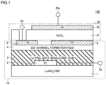
- Fig. 1 is a sectional view illustrating a configuration of a variable capacitive element 100 according to a first embodiment.
- Fig. 2 is a plan view illustrating the configuration of variable capacitive element 100 of the first embodiment.
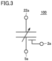
- Fig. 3 is a circuit diagram illustrating variable capacitive element 100 of the first embodiment.
- Variable capacitive element 100 in Fig. 1 includes a switch portion 10 configuring a field effect transistor formed on a semiconductor substrate 1 and an element portion 20 that is electrically connected to switch portion 10 and configures a passive element.
- Element portion 20 is provided above switch portion 10.
- Switch portion 10 includes a gate electrode 2, a gate insulating film 3, a channel formation film 4, a source electrode 5, and a drain electrode 6.
- gate electrode 2 is formed on semiconductor substrate 1
- gate insulating film 3 and channel formation film 4 are sequentially formed so as to overlap gate electrode 2
- source electrode 5 and drain electrode 6 are respectively formed on gate insulating film 3 and channel formation film 4.
- switch portion 10 is an oxide field effect transistor (FET).
- FET oxide field effect transistor
- semiconductor substrate 1 for example, lanthanum aluminate (LAO) is used, and gate electrode 2 is formed of platinum (Pt) on the lanthanum aluminate in a predetermined pattern of Fig. 2 .
- LAO lanthanum aluminate
- gate electrode 2 is formed of platinum (Pt) on the lanthanum aluminate in a predetermined pattern of Fig. 2 .
- a La-HfO 2 film having a film thickness of 70 nm is used for gate insulating film 3
- an IZO film having a film thickness of 25 nm is used for channel formation film 4.
- Source electrode 5 and drain electrode 6 are formed of platinum (Pt) in the predetermined pattern of Fig. 2 on channel formation film 4 of the IZO film.
- a terminal electrode 5a (first terminal electrode) is provided on source electrode 5 in Fig. 2
- source electrode 5 itself
- Element portion 20 is provided above switch portion 10 and includes an Al 2 O 3 film of a dielectric 21 and a terminal electrode 22 (second terminal electrode) of platinum (Pt) formed to overlap dielectric 21.
- Terminal electrode 22 is formed in the predetermined pattern of Fig. 2 .
- gate electrode 2 is extended from a region where source electrode 5 and drain electrode 6 overlap each other, and a control electrode terminal 2a is provided on gate electrode 2.
- Element portion 20 configures a first capacitor (first passive element) between source electrode 5 and terminal electrode 22, and configures a second capacitor (second passive element) at least between drain electrode 6 and terminal electrode 22.
- first capacitor is a portion C1 where source electrode 5 and terminal electrode 22 overlap each other in planar view.
- second capacitor is a portion C2 where drain electrode 6 including channel formation film 4 and terminal electrode 22 overlap each other in planar view.
- variable capacitive element 100 when switch portion 10 is in an off state, a gate voltage greater than or equal to a threshold is not applied to gate electrode 2, so that an electron depletion layer exists at a position of channel formation film 4 overlapping gate electrode 2 in planar view and source electrode 5 and drain electrode 6 are not electrically connected. For this reason, because a voltage is applied only between source electrode 5 and the portion of terminal electrode 22 opposite to source electrode 5, variable capacitive element 100 has the capacitance of only the first capacitor.
- variable capacitive element 100 when switch portion 10 is in an on state, the channel is formed by applying the gate voltage greater than or equal to the threshold to gate electrode 2, and source electrode 5 and drain electrode 6 are electrically connected. For this reason, the voltage is applied between source electrode 5 and drain electrode 6 (including channel formation film 4 therebetween) and opposing terminal electrode 22, so that variable capacitive element 100 becomes a combined capacitance of the first capacitor and the second capacitor.
- variable capacitive element 100 switch portion 10 is turned on and off to switch between the case where the first capacitor element is turned on in element portion 20 and the case where the first capacitor and a second capacitor element are turned on in element portion 20, thereby varying the capacitance of the capacitor.
- Variable capacitive element 100 is a variable capacitive element that is divided into switch portion 10 that operates on and off by the voltage applied to gate electrode 2 (control electrode terminal 2a), terminal electrode 5a (first terminal electrode), and element portion 20 that operates on terminal electrode 22 (second terminal electrode), and operates on three terminals. For this reason, the structure of variable capacitive element 100 is different from that of the variable capacitive element disclosed in NPL 1 in which the capacitance is varied by two terminals of the gate electrode and the source electrode.
- the film thickness of gate insulating film 3 is desirably reduced from the viewpoint of power consumption, and a withstand voltage decreases by reducing the film thickness, but a driving voltage decreases, so that low-voltage driving can be performed.
- variable capacitive element 100 by utilizing the structure in which gate electrode 2 of switch portion 10 and element portion 20 are electrically separated, apart from reducing the film thickness of gate insulating film 3 to achieve the low-voltage driving and the low-withstand voltage, the capacitance can be increased by making dielectric 21 thick and making dielectric 21 have a multilayer structure, and both the high-withstand voltage and high capacitance can be achieved.
- variable capacitive element 100 because gate electrode 2 (control electrode terminal 2a) of switch portion 10 is electrically separated from terminal electrode 5a (first terminal electrode) and terminal electrode 22 (second terminal electrode) of element portion 20, the operation of switch portion 10 is not affected by the signal on the side on element portion 20.
- terminal electrode 5a (first terminal electrode) of variable capacitive element 100 and a terminal 22a of terminal electrode 22 (second terminal electrode) are connected to a converter circuit or the like, while control electrode terminal 2a varying the capacitance is connected to a circuit different from the converter circuit. For this reason, there is a low possibility that the signal applied to control electrode terminal 2a is affected by the signal of the converter circuit.
- variable capacitive element 100 the electric resistance of channel formation film 4 between source electrode 5 and drain electrode 6 can be reduced by shortening channel length L of switch portion 10. Consequently, in variable capacitive element 100, improvement of the switching speed (time constant) of switch portion 10 can be coped with in order to vary the capacitance at a high speed.
- Fig. 4 is a graph illustrating a width of a variable capacitance of variable capacitive element 100 according to the first embodiment.
- the width of the capacitance that can be varied by variable capacitive element 100 depends on the capacitance of the second capacitor as described above. That is, the wider the portion C2 where drain electrode 6 and terminal electrode 22 overlap each other in planar view, the larger the capacitance of the second capacitor, and the wider the capacitance that can be varied by variable capacitive element 100.
- the graph illustrated in Fig. 4 is an actual measurement value of variable capacitive element 100 in which an area of the portion C2 where drain electrode 6 and terminal electrode 22 overlap each other in planar view is 1000 times (area ratio 1000 times) an area of the portion C 1 where source electrode 5 and terminal electrode 22 overlap each other in planar view.
- a horizontal axis represents the applied voltage (unit: V) of gate electrode 2
- a vertical axis represents the capacitance (unit: pF) of variable capacitive element 100.
- variable capacitive element 100 designed such that the capacitance of only the first capacitor becomes 0.048 pF and such that the capacitances of the first capacitor and the second capacitor become 48 pF is actually measured, the capacitance became 0.052 pF when the applied voltage of the gate electrode 2 is less than the threshold and the capacitance became 41 pF when the applied voltage is greater than or equal to the threshold as illustrated in Fig. 4 .
- FIG. 5 is a sectional view illustrating the method for manufacturing the variable capacitive element of the first embodiment.
- gate electrode 2 of platinum (Pt) having the film thickness of 80 nm is formed on a (100) plane of prepared lanthanum aluminate (LAO) semiconductor substrate 1.
- gate electrode 2 is formed by forming a photoresist of a predetermined pattern on the (100) plane of the semiconductor substrate 1 using a photolithography technique, and then forming a film of platinum (Pt) by radio-frequency (RF) sputtering, and removing the photoresist by lift-off.
- RF radio-frequency
- gate insulating film 3 having the film thickness of 70 nm is formed to overlap the surface of semiconductor substrate 1 on which gate electrode 2 is formed.
- gate insulating film 3 is formed by spin-coating a La-HfO 2 solution on the surface of semiconductor substrate 1 on which gate electrode 2 is formed using a chemical solution deposition (CSD) method, drying the film at 150°C, and then firing the film at 800°C in an oxygen atmosphere to crystallize the film.
- CSD chemical solution deposition
- channel formation film 4 having the film thickness of 25 nm is formed to overlap gate insulating film 3.
- channel formation film 4 is formed by spin-coating an IZO solution on gate insulating film 3 using the chemical solution deposition method (CSD), drying the film at 150°C, and then firing the film at 500°C in an oxygen atmosphere to crystallize the film.
- CSD chemical solution deposition method
- platinum (Pt) source electrode 5 and platinum (Pt) drain electrode 6 each having the thickness of 80 nm are formed on channel formation film 4.
- source electrode 5 and drain electrode 6 are formed by forming a photoresist of a predetermined pattern on channel formation film 4 using a photolithography technique, then forming the film of platinum (Pt) by radio-frequency (RF) sputtering, and removing the photoresist by lift-off.
- RF radio-frequency
- dielectric 21 is formed of the Al 2 O 3 film having the film thickness of 500 nm on source electrode 5 and drain electrode 6. Specifically, dielectric 21 is formed by forming the photoresist of a predetermined pattern on source electrode 5 and drain electrode 6 using the photolithography technique, then forming the Al 2 O 3 film by electron cyclotron resonance (ECR) sputtering, and removing the photoresist by lift-off.
- ECR electron cyclotron resonance
- terminal electrode 22 of platinum (Pt) having the film thickness of 80 nm is formed on dielectric 21.
- terminal electrode 22 is formed by forming the photoresist of the predetermined pattern on dielectric 21 using the photolithography technique, then forming the film of platinum (Pt) by radio-frequency (RF) sputtering, and removing the photoresist by lift-off.
- RF radio-frequency
- variable capacitive element 100 In variable capacitive element 100 described so far, the element in which the capacitance is varied by two values of the capacitance of only the first capacitor and the combined capacitance of the first capacitor and the second capacitor has been described.
- a multi-valued variable capacitive element can be configured by forming a plurality of variable capacitive elements 100 in a matrix shape on semiconductor substrate 1.
- Fig. 6 is a circuit diagram illustrating a multi-valued variable capacitive element 100a of the first embodiment.
- a multi-valued variable electronic element can be similarly configured by forming a plurality of variable electronic elements such as inductors and resistors other than capacitors as the included passive elements in a matrix shape.
- Fig. 6 illustrates a circuit diagram of variable capacitive element 100a in which n ⁇ n variable capacitive elements 100 in Fig. 3 are connected in the matrix shape.
- terminal electrode 5a first terminal electrode
- terminals 22a of terminal electrode 22 second terminal electrode
- control electrode terminal 2a of each of n ⁇ n variable capacitive elements 100 is provided separately, and terminals G11 to Gnn are illustrated in Fig. 6 .
- variable capacitive element 100 the configuration in which element portion 20 is provided on switch portion 10 as illustrated in Fig. 1 has been described. However, element portion 20 may be provided below switch portion 10. Specifically, the variable capacitive element in which element portion 20 is provided under switch portion 10 will be described.
- Fig. 7 is a sectional view illustrating configurations of variable capacitive elements 100b, 100c according to a modification of the first embodiment. In variable capacitive elements 100b, 100c of Fig. 7 , the same components as those of variable capacitive element 100 in Fig. 1 are denoted by the same reference numerals, and the detailed description thereof will not be repeated.
- Fig. 7(a) illustrates a variable capacitive element 100b in which a multi-layer ceramic capacitor (MLCC) is used for element portion 20b.
- MLCC multi-layer ceramic capacitor
- source electrode 5 and drain electrode 6 are formed on the upper surface of the multi-layer ceramic capacitor of element portion 20b, and channel formation film 4, gate insulating film 3, and gate electrode 2 are formed on source electrode 5 and drain electrode 6 in this order to constitute switch portion 10.
- the multi-layer ceramic capacitor of element portion 20b includes a portion of the first capacitor connected to source electrode 5 and a portion of the second capacitor connected to drain electrode 6.
- the portion of the first capacitor has a configuration in which a plurality of electrodes 25b connected to source electrode 5 and an electrode 24b connected to a terminal electrode 22b that is an external electrode of the multi-layer ceramic capacitor are laminated with, for example, a dielectric 21b of barium titanate interposed therebetween.
- the portion of the second capacitor has a configuration in which a plurality of electrodes 23b connected to drain electrode 6 and electrodes 24b connected to terminal electrode 22b are laminated with dielectric 21b interposed therebetween.
- variable capacitive element 100b similarly to variable capacitive element 100, when switch portion 10 is in the off state, a gate voltage greater than or equal to the threshold is not applied to gate electrode 2, so that the electron depletion layer exists at the position of channel formation film 4 overlapping gate electrode 2 in planar view and source electrode 5 and drain electrode 6 are not electrically connected. Therefore, the voltage is applied only to dielectric 21b between electrode 25b connected to source electrode 5 and electrode 24b connected to terminal electrode 22b, so that variable capacitive element 100b has the capacitance of only the first capacitor.
- variable capacitive element 100b when switch portion 10 is in the on state, the channel is formed by applying the gate voltage greater than or equal to the threshold to gate electrode 2, and source electrode 5 and drain electrode 6 are electrically connected. Consequently, the voltage is applied to dielectric 21b between electrode 25b connected to source electrode 5 and electrode 23b connected to drain electrode 6, and electrode 24b connected to terminal electrode 22b, so that variable capacitive element 100b has the combined capacitance of the first capacitor and the second capacitor.
- LTCC low temperature co-fired ceramics
- HTCC high temperature co-fired ceramics
- Fig. 7(b) illustrates a variable capacitive element 100c using a silicon capacitor as an element portion 20c.
- source electrode 5 and drain electrode 6 are formed on the upper surface of the silicon capacitor of element portion 20c, and channel formation film 4, gate insulating film 3, and gate electrode 2 are formed thereon in this order to configure switch portion 10.
- the silicon capacitor of element portion 20c is formed by a semiconductor process, and is configured of an N+ layer 24c formed by implanting n-type impurity ions into a silicon substrate 1a, a dielectric 21c formed on the surface of N+ layer, and a polysilicon layer 23c that is formed on the surface of dielectric 21c and connected to a polysilicon layer 25c connected to source electrode 5 or drain electrode 6.
- dielectric 21c is made of an inorganic material such as silicon oxide, silicon nitride, hafnium oxide, hafnium silicate, alumina, or barium titanate formed by a chemical vapor deposition (CVD) method.
- a plurality of trenches or a plurality of pillars are formed in silicon substrate 1a to form an uneven shape.
- the silicon capacitor of element portion 20c includes a portion of the first capacitor connected to source electrode 5 and a portion of the second capacitor connected to drain electrode 6.
- the portion of the first capacitor is configured of a portion of dielectric 21c sandwiched between polysilicon layer 25c connected to source electrode 5 and N+ layer 24c connected to terminal electrode 22c.
- the portion of the second capacitor is configured of a portion of dielectric 21c sandwiched between polysilicon layer 23c connected to drain electrode 6 and N+ layer 24c connected to terminal electrode 22c.
- variable capacitive element 100c similarly to variable capacitive element 100, when switch portion 10 is in the off state, the gate voltage greater than or equal to the threshold is not applied to gate electrode 2, so that the electron depletion layer exists at the position of channel formation film 4 overlapping gate electrode 2 in planar view and source electrode 5 and drain electrode 6 are not electrically connected. Therefore, the voltage is applied only to a portion of dielectric 21c sandwiched between polysilicon layer 25c connected to source electrode 5 and N+ layer 24c connected to terminal electrode 22c, so that variable capacitive element 100c has the capacitance of only the first capacitor.
- variable capacitive element 100c when switch portion 10 is in the on state, the channel is formed by applying the gate voltage greater than or equal to the threshold to gate electrode 2, and source electrode 5 and drain electrode 6 are electrically connected. Accordingly, the voltage is applied to a portion of dielectric 21c sandwiched between polysilicon layer 25c connected to source electrode 5 and polysilicon layer 23c connected to drain electrode 6, and N+ layer 24c connected to terminal electrode 22c, so that variable capacitive element 100c becomes the combined capacitance of the first capacitor and the second capacitor.
- the capacitance of element portion 20c is increased by providing an uneven portion in silicon substrate 1a.
- dielectric 21c may have a parallel flat plate shape as long as the required capacitance can be secured.
- variable capacitive element 100 of the first embodiment includes switch portion 10 configuring the field effect transistor, and element portion 20 that is electrically connected to switch portion 10 and configures the capacitor (passive element).
- Switch portion 10 includes source electrode 5, drain electrode 6, channel formation film 4 formed so as to overlap at least a part of source electrode 5 and a part of drain electrode 6, gate insulating film 3 formed so as to overlap channel formation film 4, and gate electrode 2 formed so as to overlap gate insulating film 3.
- Element portion 20 includes terminal electrode 5a (first terminal electrode) electrically connected to source electrode 5, and terminal electrode 22 (second terminal electrode) that configures the first capacitor (first passive element) with source electrode 5 and configures the second capacitor (second passive element) at least with drain electrode 6.
- variable capacitive element 100 can change the capacitance of the capacitor by switching between the case where element portion 20 is configured by the first capacitor and the case where element portion 20 is configured by the first capacitor and the second capacitor by turning on and off of switch portion 10.
- Switch portion 10 is preferably provided on the upper portion or the lower portion of element portion 20.
- variable capacitive element 100 of the first embodiment the first capacitor is configured between source electrode 5 and terminal electrode 22, and the second capacitor is configured between drain electrode 6 and terminal electrode 22, so that the range in which the capacitance of the capacitor can be varied can be widened and the sufficient withstand voltage can be obtained without reducing the capacitance of the capacitor.
- element portion 20 further includes dielectric 21 provided so as to overlap source electrode 5 and drain electrode 6, dielectric 21 between source electrode 5 and terminal electrode 22 configures the first capacitor serving as the first passive element, and at least dielectric 21 between drain electrode 6 and terminal electrode 22 configures the second capacitor serving as the second passive element.
- gate electrode 2 is formed on semiconductor substrate 1
- gate insulating film 3 is formed on gate electrode 2 and semiconductor substrate 1
- channel formation film 4 is formed on gate insulating film 3
- source electrode 5 and drain electrode 6 are formed on channel formation film 4
- dielectric 21 is formed on source electrode 5 and drain electrode 6, and terminal electrode 22 is formed on dielectric 21.
- the included passive element is the capacitor, and the variable capacitive element capable of varying the capacitance has been described.
- the included passive element is not limited to the capacitor.
- the included passive element is an inductor, and a variable inductance element capable of varying inductance will be described with reference to the drawings.
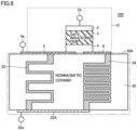
- Fig. 8 is a sectional view illustrating a configuration of a variable inductance element 200 of the second embodiment.
- Fig. 9 is a circuit diagram illustrating variable inductance element 200 of the second embodiment.
- variable inductance element 200 of Figs. 8 and 9 the same components as those of variable capacitive element 100 of Figs. 1 and 3 are denoted by the same reference numerals, and a detailed description thereof will not be repeated.
- Variable inductance element 200 in Fig. 8 includes switch portion 10 configuring the field effect transistor, and an element portion 20A that is electrically connected to switch portion 10 and configures the passive element. Element portion 20A is provided below switch portion 10.
- Switch portion 10 includes a gate electrode 2, a gate insulating film 3, a channel formation film 4, a source electrode 5, and a drain electrode 6.
- source electrode 5 and drain electrode 6 are formed on the upper surface of element portion 20A, and channel formation film 4, gate insulating film 3, and gate electrode 2 are formed on source electrode 5 and drain electrode 6 in this order to configure switch portion 10.
- element portion 20A is an inductor, and includes a portion of the first inductor connected to source electrode 5 and a portion of the second inductor connected to drain electrode 6.
- the portion of the first inductor includes a coil electrode 23 connected to source electrode 5 and a terminal electrode 22A that is an external electrode of the inductor.
- the portion of the second inductor includes a coil electrode 24 connected to drain electrode 6 and terminal electrode 22A that is the external electrode of the inductor.
- Coil electrode 23 and coil electrode 24 are formed in the same nonmagnetic ceramic 25.
- control electrode terminal 2a is provided on gate electrode 2 in Fig. 8
- gate electrode 2 itself may be used as control electrode terminal 2a.
- terminal 22a of terminal electrode 22A is provided on terminal electrode 22A in Fig. 8
- terminal electrode 22A itself may be used as terminal 22a.
- variable inductance element 200 similarly to variable capacitive element 100, when switch portion 10 is in the off state, the gate voltage greater than or equal to the threshold is not applied to gate electrode 2, so that the electron depletion layer at the position of channel formation film 4 overlapping gate electrode 2 in planar view and source electrode 5 and drain electrode 6 are not electrically connected. Consequently, the current flows only through coil electrode 24 between source electrode 5 and terminal electrode 22A, so that variable inductance element 200 has the inductance of only the first inductor.
- variable inductance element 200 when switch portion 10 is in the on state, the channel is formed by applying the gate voltage greater than or equal to the threshold to gate electrode 2, and source electrode 5 and drain electrode 6 are electrically connected. Consequently, the current flows through coil electrode 23 between source electrode 5 and terminal electrode 22A, and coil electrode 24 between drain electrode 6 and terminal electrode 22A, so that variable inductance element 200 has the combined inductance of the first inductor and the second inductor.
- variable inductance element 200 terminal electrode 5a (first terminal electrode) and terminal 22a of terminal electrode 22A (second terminal electrode) are connected to the converter circuit or the like, and control electrode terminal 2a varying the inductance is connected to a circuit different from the converter circuit. For this reason, there is a low possibility that the signal applied to control electrode terminal 2a is affected by the signal of the converter circuit.
- the passive element is an inductor
- element portion 20A includes the first inductor that is electrically connected between source electrode 5 and terminal electrode 22A and serves as the first passive element, and the second inductor that is electrically connected between drain electrode 6 and terminal electrode 22A and serves as the second passive element.
- variable inductance element 200 of the second embodiment the first inductor is configured between source electrode 5 and terminal electrode 22A, and the second inductor is configured between drain electrode 6 and terminal electrode 22A, so that the range in which the inductance of the inductor can be varied can be widened and the sufficient withstand voltage can be obtained without reducing the inductance of the inductor.
- a multi-valued variable inductance element may be configured by forming a plurality of variable inductance elements 200 in a matrix shape.
- the passive element may be used as a variable resistor element as a resistor.
- the configuration of switch portion 10 described in the first embodiment and the second embodiment is not limited to the described configuration, but for example, may be a silicon MOSFET, a GaNFET, or the like.
- variable capacitive elements 100, 100a and variable inductance element 200 have, due to the configuration thereof, the wide width in which the physical quantity of the passive element can be varied, and have the characteristic in which the sufficient withstand voltage can be obtained without reducing the physical quantity of the passive element.
- a circuit device including variable capacitive element 100, 100a and variable inductance element 200 using this characteristic will be described below.
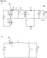
- Fig. 10 is a circuit diagram illustrating a circuit device according to a third embodiment.
- Fig. 10(b) is an equivalent circuit in Fig. 10(a) .
- a circuit device 300 in Fig. 10(a) is a circuit that adjusts an output level according to a load variation, and is an LLC resonance converter.
- Circuit device 300 that is the LLC resonant converter can convert an input voltage Vin into an output voltage Vout.
- Circuit device 300 includes switching elements Q1, Q2, a transformer T, a resonance capacitor Cr, leakage inductors Lr, Lr1, Lr2, an excitation inductor Lm, output rectifier diodes D1, D2, and an output capacitor C0.
- Output capacitor C0 is connected to a load resistor R0.
- the input-output voltage ratio of the LLC resonant converter can be adjusted by modulating a switching frequency f of switching elements Q1, Q2.
- the output voltage (Vout) of the LLC resonant converter is normally adjusted by operating the LLC resonant converter at a frequency greater than or equal to the frequency at which the input-output voltage ratio becomes the maximum value and changing the switching frequency according to a load variation.
- the LLC resonant converter needs to have the switching frequency greater than the frequency at which the input-output voltage ratio becomes a maximum value.
- the power loss of the LLC resonant converter depends on the switching frequency, there is a problem that the power loss increases when the switching frequency is increased to lower the output voltage (Vout) of the LLC resonant converter.
- variable capacitive element 100 of the first embodiment is used for resonance capacitor Cr in order to lower the output voltage (Vout) of the LLC resonance converter without increasing the switching frequency.
- Circuit device 300 can lower the output voltage (Vout) without increasing the switching frequency by using variable capacitive element 100 as resonance capacitor Cr.
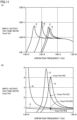
- Fig. 11 is a graph illustrating a frequency characteristic of circuit device 300 of the third embodiment.
- Fig. 11(a) illustrates frequency characteristics of the input-output voltage ratio when the capacitance is 1.5 times, 10 times, and 100 times the capacitance of resonance capacitor Cr (for example, 0.02 ⁇ F).
- Fig. 11(b) is an enlarged view of a part of the graph in Fig. 11(a) .
- the horizontal axis represents an operation frequency (unit: Hz)
- the vertical axis represents the input-output voltage ratio.
- a graph A illustrates the frequency characteristic of the input-output voltage ratio when the capacitance of resonance capacitor Cr is 100 times
- the capacitance of resonance capacitor Cr is 10 times
- a graph B illustrates the frequency characteristic of the input-output voltage ratio when the capacitance of the resonance capacitor Cr is increased by 1.5 times
- a graph D illustrates the frequency characteristic of the input-output voltage ratio when the capacitance of resonance capacitor Cr remains.
- the input-output voltage ratios illustrated when graphs A to D have the same operation frequency greatly change.
- the input-output voltage ratio of graph D is
- 4.0
- the input-output voltage ratio of graph C is
- 2.2
- the input-output voltage ratio of graph B is
- 0.9
- the input-output voltage ratio of graph A is
- 0.8. That is, by varying the capacitance of resonance capacitor Cr by about 10 times, the input-output voltage ratio can be changed in the range of 4.0 to 0.9 without changing the operating frequency.
- variable capacitive element 100 as resonance capacitor Cr of circuit device 300
- the output voltage (Vout) can be lowered without increasing the power loss.
- the capacitance of resonance capacitor Cr can be dynamically varied, and the input-output voltage ratio can be changed to multiple stages.
- the LLC resonant converter has a circuit configuration in which the LC resonance is used as illustrated in Fig. 10 , and can implement low-loss soft switching by the circuit configuration.
- variable capacitive element 100 as resonance capacitor Cr, for example, even for a switching amplifier (such as a pulse width modulation (PWM) amplifier), the loss at the switching time can be greatly reduced by dynamically changing the capacitance of resonance capacitor Cr.
- PWM pulse width modulation
- Fig. 12 is a block diagram illustrating a circuit device according to a fourth embodiment.
- the circuit device in Fig. 12 is a switching amplifier, and uses the LLC resonance converter in which resonance capacitor Cr is used as variable capacitive element 100 for a class-D output stage 301.
- resonance capacitor Cr variable capacitive element 100
- the capacitive impedance after class-D output stage 301 can be reduced to implement the low-loss soft switching.
- Fig. 13 is a timing chart illustrating switching timing of the circuit device of the fourth embodiment.
- the switching in Fig. 13(a) is referred to as hard switching.
- the PWM can be turned on (zero voltage switching (ZVS)) in the state where voltage V DS is zero.
- ZVS zero voltage switching
- the PWM can be turned on (zero current switching (ZCS)) in the state where the current I D is zero. Consequently, the switching loss can be reduced in the LLC resonance converter.
- the switching Fig. 13(b) is referred to as soft switching.
- the LLC resonant converter (circuit device 300) in Fig. 10 has two resonance frequencies of a resonance frequency fr of resonance capacitor Cr and leakage inductor Lr and a resonance frequency fm of resonance capacitor Cr, leakage inductor Lr, and excitation inductor Lm.
- a condition that the soft switching state is established is determined by the relationship between resonance frequencies fr, fm and switching frequency f. For example, when switching frequency f is lower than resonance frequency fm (f ⁇ fm), circuit device 300 satisfies the hard switching condition. However, this condition is not normally used because gain inversion is generated.
- circuit device 300 that is the LLC resonance converter
- the condition that the soft switching state is satisfied varies depending on the load condition and is determined by conditional expressions illustrated in (Expression 4) and (Expression 5).
- variable capacitive element 100 is used for resonance capacitor Cr. As described in the first embodiment, variable capacitive element 100 has a wider variable capacitance range than the conventional variable capacitive element, so that large fluctuations in input voltage Vin and the load condition can be coped with.
- variable capacitive element 100 for resonance capacitor Cr of circuit device 300 the capacitance of resonance capacitor Cr can be greatly varied, and a wide range of the conditions that the soft switching holds can be secured.
- the capacitance of resonance capacitor Cr can be dynamically varied, and the condition that the soft switching is satisfied can be adjusted in multiple stages.
- variable inductance element described in the second embodiment for leakage inductor Lr and excitation inductor Lm in addition to the use of variable capacitive element 100 for resonance capacitor Cr of circuit device 300.
- the circuit device capable of adjusting the condition that the soft switching is satisfied by varying resonance capacitor Cr or the like is not limited to circuit device 300 that is the LLC resonance converter, and can also be applied to circuit devices of various resonance systems such as a current resonance circuit, a voltage resonance circuit, a multiple resonance circuit, a series resonance circuit, and a parallel resonance circuit.
- variable capacitive element described in the first embodiment and the variable inductance element described in the second embodiment are applied to a multi-band wireless communication terminal will be described below.
- IoT Internet of Things
- a very wide frequency band of about several 10 MHz to 5 GHz is required to be used in one wireless communication terminal in order to communicate large-capacity and high-density data.
- the wireless communication terminal a plurality of RF circuits that needs to be multi-band and correspond to each frequency are required to be provided, and the RF circuit to be used is required to be appropriately switched.
- the wireless communication terminal increases in a circuit scale and the number of components, and it becomes difficult to reduce the size and cost of the terminal.
- the circuit scale and the number of components are required to be reduced by sharing a circuit block for a plurality of frequencies.
- the circuit block is shared for the plurality of frequencies, signal reflection between the circuit blocks is required to be prevented, and impedance matching is required to be performed according to each frequency.
- the resonance frequency of the antenna is required to be significantly modulated.
- the capacitance value of the capacitor is varied in order to perform the impedance matching and modulation of the resonance frequency, a plurality of frequency bands can be covered while the circuit scale and the number of components are reduced.
- Variable capacitive element 100 of the first embodiment can have the wider range of capacitance that can be varied than the conventional variable capacitive element. Consequently, the wireless communication terminal using variable capacitive element 100 can cover the wide frequency band.
- the capacitance value of variable capacitive element 100 is switched by the voltage applied to the control electrode terminal 2a, so that the capacitance value does not change nonlinearly (gently) with respect to the voltage unlike the conventional variable capacitive element. For this reason, in the wireless communication terminal using variable capacitive element 100, a distortion signal is not generated, and a disturbance signal is not generated for other frequencies.
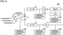
- Circuit device 400 is a communication circuit block provided in the wireless communication terminal, and can be used for sharing a plurality of frequencies. For this reason, in circuit device 400, variable capacitive element 100 is applied to the capacitor in which the capacitance value is required to be variable in order to perform the impedance matching and the modulation of the resonance frequency.
- variable capacitive element 100 can vary the capacitance in the range of 10 times to 1000 times, so that the impedance matching and the modulation of the resonance frequency can be performed in the wider range to cover a wider reception frequency band. Furthermore, in circuit device 400, variable capacitive element 100 digitally varies the capacitance, so that the distortion signal can be prevented. Consequently, using circuit device 400, the multi-band wireless communication terminal capable of covering the plurality of frequency bands can be implemented while the circuit scale and the number of components are reduced. Multi-valued variable capacitive element 100a may be used for the capacitor of circuit device 400.
- the configuration of the DC circuit breaker can be similarly applied to switches, connection devices, and arc prevention devices of various power supply circuits.
- the DC circuit breaker can be used in a DC power supply device such as an energy harvesting device such as solar power generation, a fuel cell, or a lithium ion cell.
- a power semiconductor switch using silicon carbide (SiC) or gallium nitride (GaN) capable of high-withstand voltage, high temperature operation, and high speed operation as compared with the MOSFET is expected to be used instead of the metal contact.
- SiC silicon carbide
- GaN gallium nitride
- the switching of about several 100 V to several 10 A is possible when a power semiconductor switch is used in the DC circuit breaker instead of the metal contact, but there is a problem that an energization loss due to heat generation at the time of energization of the semiconductor becomes very large and the provision of a cooling device is required.
- Circuit device 500 is a hybrid switch circuit used for the DC circuit breaker, and includes a metal contact S1 and a semiconductor switch S2 of the MOSFET.
- metal contact S1 can be opened and closed without arc discharge, there is an advantage that no contact exhaustion, a long life, and high-speed current cut off can be performed, and the noise due to the arc discharge is not generated.
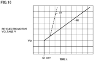
- Fig. 16 is a graph illustrating a switching characteristic of the circuit device 500 of the sixth embodiment.
- the horizontal axis represents time t
- the vertical axis represents re-electromotive voltage V.
- a graph R1 in Fig. 16 after metal contact S1 is turned off, re-electromotive voltage V of metal contact S1 increases linearly with respect to time t.
- the capacitance of capacitor C is required to set to the relatively large capacitance (for example, several 10 nF) in order to absorb the electric charge that generates the arc discharge.
- variable capacitive element described in the first embodiment is used for capacitor C such that the capacitance of capacitor C can be largely varied between the on state and the off state of metal contact S1. Consequently, the DC circuit breaker in which the circuit loss is very low while the arc discharge is prevented is implemented in circuit device 500.
- the high-withstand voltage can be obtained while the capacitance is varied in the wide range that has been difficult to be implemented in the conventional variable capacitive element.
- Multi-valued variable capacitive element 100a may be used for capacitor C of circuit device 500.
- switch portion 10 included gate electrode 2, gate insulating film 3, channel formation film 4, source electrode 5, and drain electrode 6.
- drain electrode 6 is a floating electrode, and can configure a switch portion in which drain electrode 6 not provided.
- a configuration in which the drain electrode as the floating electrode is not provided will be described with reference to the drawings.
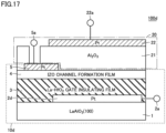
- Fig. 17 is a sectional view illustrating a configuration of a variable capacitive element 100d of the seventh embodiment.
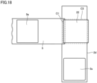
- Fig. 18 is a plan view illustrating the configuration of variable capacitive element 100d of the seventh embodiment.
- variable capacitive element 100d of Figs. 17 and 18 the same components as those of variable capacitive element 100 in Figs. 1 and 2 are denoted by the same reference numerals, and the detailed description thereof will not be repeated.
- a variable capacitive element 100d in Fig. 17 includes a switch portion 10d configuring the field effect transistor formed on semiconductor substrate 1, and element portion 20 that is electrically connected to switch portion 10d and configures the passive element. Element portion 20 is provided above switch portion 10d.
- Switch portion 10d includes a gate electrode 2d, gate insulating film 3, channel formation film 4, and source electrode 5.
- gate electrode 2d is formed on semiconductor substrate 1
- gate insulating film 3 and channel formation film 4 are sequentially formed so as to overlap gate electrode 2d
- source electrode 5 is formed on gate insulating film 3 and channel formation film 4.
- variable capacitive element 100d when switch portion 10d is turned on, the gate voltage is applied to gate electrode 2d, and the channel charges are generated in a portion of channel formation film 4 overlapping gate electrode 2d in planar view.
- the capacitance is formed by applying the voltage between a portion of source electrode 5 and channel formation film 4, and terminal electrode 22 opposite the portion.
- variable capacitive element 100d has the capacitance of only the first capacitor.
- Element portion 20 constitutes the first capacitor (first passive element) between source electrode 5 and terminal electrode 22, and configures the second capacitor (second passive element) between gate electrode 2d and terminal electrode 22.
- the first capacitor is a portion C1 where source electrode 5 and terminal electrode 22 overlap each other in planar view.
- the second capacitor is a portion C3 where gate electrode 2d and terminal electrode 22 overlap each other in planar view.
- variable capacitive element 100d by turning on and off switch portion 10d, the capacitance of the capacitor can be varied by switching between the case where the first capacitor element is used as element portion 20 and the case where the first capacitor element and the second capacitor element are used as element portion 20.
- variable capacitive element 100d is the variable capacitive element that is divided into switch portion 10d that performs the on and off operation by the voltage applied to gate electrode 2d (control electrode terminal 2a), terminal electrode 5a (first terminal electrode), element portion 20 that operates with terminal electrode 22 (second terminal electrode), and operates with three terminals.
- variable capacitive element 100d because the capacitance of the second capacitor element can be changed by the channel charge generated in channel formation film 4 without providing the drain electrode, the capacitance of the second capacitor element can be continuously varied by the voltage applied to gate electrode 2d.
- the residual charge in the floating electrode is reduced at the time of the on and off operation of switch portion 10d by adopting the configuration in which the drain electrode that is the floating electrode is not provided, so that the potential of the capacitor can be stabilized or the failure due to short-circuiting can be reduced.
- variable capacitive element 100d the drain electrode that is the floating electrode is not provided, the conductivity can be varied stepwise in the wide region of channel formation film 4 according to the level of the gate voltage to be applied, so that the capacitance of the capacitor can be changed more continuously.
- variable capacitive element 100d of the seventh embodiment uses the portion C3 where gate electrode 2d and channel formation film 4 overlap each other in planar view instead of the drain electrode.
- the second capacitor element is formed between portion C3 and terminal electrode 22.
- variable capacitive element 100d can continuously vary the capacitance of the second capacitor element.
- variable capacitive element 100d the configuration in which element portion 20 is provided on switch portion 10d as illustrated in Fig. 17 has been described, but element portion 20 may be provided under switch portion 10d.
- a multi-valued variable electronic element may be similarly configured by forming a plurality of variable capacitive elements 100d in a matrix shape.
- the configuration of variable capacitive element 100d may be applied to a variable electronic element other than a capacitor, such as an inductor or a resistor.
- variable capacitive element 100 of the first embodiment terminal electrode 22 is also formed on the channel region formed between source electrode 5 and drain electrode 6. Accordingly, variable capacitive element 100 sometimes affects the on and off state of switch portion 10 by the voltage applied to terminal 22a of terminal electrode 22. That is, in variable capacitive element 100, there has been a risk that the capacitance value fluctuates due to a signal between terminal electrode 5a (first terminal electrode) and terminal 22a of terminal electrode 22 (second terminal electrode).
- Fig. 19 is a sectional view illustrating a configuration of a variable capacitive element 100e of the eighth embodiment.
- Fig. 20 is a plan view illustrating the configuration of variable capacitive element 100e of the eighth embodiment.
- variable capacitive element 100e of Figs. 19 and 20 the same components as those of variable capacitive element 100 in Figs. 1 and 2 are denoted by the same reference numerals, and the detailed description thereof will not be repeated.
- Variable capacitive element 100e in Fig. 19 includes a switch portion 10 configuring a field effect transistor formed on a semiconductor substrate 1 and an element portion 20e that is electrically connected to switch portion 10 and configures the passive element.
- Element portion 20e is provided above switch portion 10.
- Element portion 20e includes the Al 2 O 3 film of dielectric 21 and a terminal electrode 22e (second terminal electrode) of platinum (Pt) formed to overlap dielectric 21.
- terminal electrode 22e is formed in a pattern avoiding the channel region formed between source electrode 5 and drain electrode 6. For this reason, in the sectional view of Fig. 19 , a terminal electrode 22e1 formed on the upper portion of source electrode 5 and a terminal electrode 22e2 formed on the upper portion of drain electrode 6 are illustrated separately.
- Element portion 20e constitutes the first capacitor (first passive element) between source electrode 5 and terminal electrode 22e1, and configures the second capacitor (second passive element) between drain electrode 6 and terminal electrode 22e2.
- the first capacitor is portion C1 where source electrode 5 and terminal electrode 22e1 overlap each other in planar view.
- the second capacitor is a portion C4 where drain electrode 6 and terminal electrode 22e2 overlap each other in planar view.
- variable capacitive element 100e when switch portion 10 is in the off state, the gate voltage greater than or equal to the threshold is not applied to gate electrode 2, so that the electron depletion layer exists at the position of channel formation film 4 overlapping gate electrode 2 in planar view and source electrode 5 and drain electrode 6 are not electrically connected. For this reason, the voltage is applied only between source electrode 5 and the portion (first region) of terminal electrode 22e1 opposite to source electrode 5, so that variable capacitive element 100e has the capacitance of only the first capacitor.
- variable capacitive element 100e when switch portion 10 is in the on state, the channel is formed by applying the gate voltage equal to greater than or equal to the threshold to gate electrode 2, and source electrode 5 and drain electrode 6 are electrically connected. For this reason, the voltage is applied between source electrode 5 and drain electrode 6, and terminal electrode 22e (first region + second region) opposite to each other, so that the variable capacitive element 100e has the combined capacitance of the first capacitor and the second capacitor.
- terminal electrode 22e a portion overlapping source electrode 5 in planar view is referred to as the first region (terminal electrode 22e1), and a portion overlapping the drain electrode in planar view is referred to as the second region (terminal electrode 22e2).
- variable capacitive element 100e Because terminal electrode 22e does not overlap the channel region formed between source electrode 5 and drain electrode 6 in planar view, the capacitance of variable capacitive element 100e is smaller than that of variable capacitive element 100 in Fig. 1 when switch portion 10 is in the on state. However, as described above, in variable capacitive element 100e, the capacitance value is less likely to fluctuate due to the signal between terminal electrode 5a (first terminal electrode) and terminal 22a of terminal electrode 22 (second terminal electrode). As a matter of course, in variable capacitive element 100e, even when terminal electrode 22e is not formed in the pattern that bypasses the entire portion of the channel region formed between source electrode 5 and drain electrode 6 as illustrated in Fig. 20 , the variation in the capacitance value due to the signal between the first terminal electrode and the second terminal electrode can be prevented even in the pattern overlapping a part of the channel region.
- terminal electrode 22e has the first region overlapping source electrode 5 in planar view and the second region overlapping drain electrode 6 in planar view, and the first region and the second region are electrically connected while bypassing at least one part of the channel region formed between source electrode 5 and drain electrode 6.
- terminal electrode 22e bypasses at least one part of the channel region formed between source electrode 5 and drain electrode 6 means that the terminal electrode has a portion that does not overlap at least one part of the channel region in planar view.
- variable capacitive element 100e the configuration in which element portion 20e is provided on switch portion 10 as illustrated in Fig. 19 has been described. However, element portion 20e may be provided below switch portion 10.
- a multi-valued variable electronic element may be similarly configured by forming a plurality of variable capacitive elements 100e in a matrix shape. Furthermore, the configuration of variable capacitive element 100e may be applied to a variable electronic element such as an inductor or a resistor other than the capacitor.
- a variable capacitive element 100f is formed in the pattern avoiding the channel region formed between source electrode 5 and drain electrode 6.
- the dielectric may also be formed in the pattern avoiding the channel region in accordance with the pattern of the terminal electrode.
- Fig. 21 is a sectional view illustrating a configuration of a variable capacitive element 100f according to a modification of the eighth embodiment.
- variable capacitive element 100f of Fig. 21 the same components as those of variable capacitive element 100e in Figs. 19 and 20 are denoted by the same reference numerals, and the detailed description thereof will not be repeated.
- a variable capacitive element 100f illustrated in Fig. 21 includes a switch portion 10 configuring the field effect transistor formed on semiconductor substrate 1, and an element portion 20f electrically connected to switch portion 10 and configuring the passive element. Element portion 20f is provided above switch portion 10.
- Element portion 20f includes the Al 2 O 3 film of a dielectric 21f and terminal electrode 22e (second terminal electrode) of platinum (Pt) formed to overlap dielectric 21f.
- terminal electrode 22e is formed in a pattern avoiding the channel region formed between source electrode 5 and drain electrode 6.
- Dielectric 21f is formed in the pattern avoiding the channel region formed between source electrode 5 and drain electrode 6 in accordance with the pattern of terminal electrode 22e. Therefore, in the sectional view of Fig. 21 , a dielectric 21f1 and terminal electrode 22e1 formed on the upper portion of source electrode 5 are illustrated separately from a dielectric 21f2 and terminal electrode 22e2 formed on the upper portion of drain electrode 6.
- dielectric 21f is formed so as to avoid at least one part of the channel region formed between source electrode 5 and drain electrode 6 in accordance with the pattern of terminal electrode 22e.
- ⁇ is each frequency. That is, the switching speed can be improved by reducing parasitic resistance R and capacitor C (parasitic capacitance).
- R ⁇ (L / (Wt)).
- ⁇ is a material-specific resistivity of channel formation film 4
- L is a channel length
- W is a channel width
- t is a film thickness of channel formation film 4.
- parasitic resistance R depends on the value of channel length L / channel width W. Consequently, the Q factor can be improved by increasing channel width W with respect to channel length L.
- source electrode 5 and drain electrode 6 are provided on channel formation film 4 as illustrated in Fig. 2 , so that channel length L and channel width W can be easily changed by the device design.
- capacitor C corresponds to the capacitance of gate insulating film 3 of switch portion 10, is proportional to the relative dielectric constant of gate insulating film 3, and is inversely proportional to the film thickness. Consequently, switch portion 10 has the structure separated from element portion 20, so that capacitor C (parasitic capacitance) can be individually adjusted.
- variable capacitive element 100 of the first embodiment when channel length L is 10 ⁇ m, when channel width W is 100 ⁇ m, when parasitic resistance R is 1 k ⁇ , and when capacitor C (parasitic capacitance) is 10 pF, the Q value is 0.02 at 1 MHz.
- channel length L is miniaturized to 1 ⁇ m
- channel width W is 1000 ⁇ m
- the film thickness of gate insulating film 3 is 10 times (7000 ⁇ m)
- the relative permittivity of gate insulating film 3 is 1/5 (about 40 ⁇ 50)
- the Q value is 100. Consequently, the switching speed of switch portion 10 can be improved to 5000 times.
- the IZO film is used for channel formation film 4, but this is an example, and another film such as an ITO film may be used.
- the La-HfO 2 film is used for gate insulating film 3, but this is an example, and another film such as a Ce-HfO 2 film may be used.
- channel formation film 4 is formed below source electrode 5 and drain electrode 6 as illustrated in Fig. 1 (top contact structure).
- the top contact structure is a structure in which the upper side of channel formation film 4 is in contact with source electrode 5 and drain electrode 6 when viewed from the side of gate electrode 2.
- channel formation film 4 may be formed on the upper side of source electrode 5 and drain electrode 6 in variable capacitive element 100 (bottom contact structure).
- the bottom contact structure is a structure that is in contact with source electrode 5 and drain electrode 6 on the lower side of channel formation film 4 when viewed from the side of gate electrode 2.
- variable electronic element 100 for example, as illustrated in Fig. 1 , the bottom gate structure in which gate electrode 2 is formed on semiconductor substrate 1, gate insulating film 3 and channel formation film 4 are sequentially formed so as to overlap gate electrode 2, and source electrode 5 and drain electrode 6 are respectively formed on gate insulating film 3 and channel formation film 4 is adopted in variable capacitive element 100.
- the present invention is not limited thereto, but the variable electronic element may adopt a top gate structure.
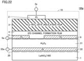
- Fig. 22 is a sectional view illustrating a configuration of a variable capacitive element 100g according to a modification. In variable capacitive element 100g, as illustrated in Fig. 22 , element portion 20 is provided below switch portion 10.
- Switch portion 10 adopts the top gate structure in which source electrode 5 and drain electrode 6 are formed on dielectric 21, channel formation film 4 and gate insulating film 3 are sequentially formed so as to overlap source electrode 5 and drain electrode 6, and gate electrode 2 is formed on gate insulating film 3.
- variable capacitive element 100g of Fig. 22 the same components as those of the variable capacitive element 100 in Fig. 1 are denoted by the same reference numerals, and the detailed description thereof will not be repeated.
- variable capacitive element 100g having the top gate structure the top contact structure in which source electrode 5 and drain electrode 6 are in contact with each other on the upper side of channel formation film 4 when viewed from the side of gate electrode 2 is adopted as illustrated in Fig. 22 .
- the present invention is not limited thereto, and the bottom contact structure in contact with source electrode 5 and drain electrode 6 on the lower side of channel formation film 4 when viewed from the side of gate electrode 2 may be adopted even in variable capacitive element 100g having the top gate structure.
- gate insulating film 3 and dielectric 21 Materials that can be adopted for gate insulating film 3 and dielectric 21 will be collectively listed below. Of course, the material is not limited to the following description.
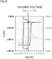
- variable capacitive elements 100 to 100g described in the above-described embodiments when a ferroelectric film such as a La-HfO 2 film is used for gate insulating film 3, the configuration of the ferroelectric gate transistor is included. For this reason, variable capacitive elements 100 to 100g have memory characteristics derived from the configuration of the ferroelectric gate transistor. Specifically, in variable capacitive element 100 of Fig. 1 , a capacitance value C on generated when an on voltage (for example, +10 V) is applied to gate electrode 2 to configure the capacitor between terminal electrode 22 and drain electrode 6 can be held only by applying a holding voltage of 0 (zero) V or a small constant value (for example, -1.0 V) to gate electrode 2.
- an on voltage for example, +10 V
- variable capacitive element 100 a capacitance value C off generated when an off voltage (for example, -10 V) is applied to gate electrode 2 and the capacitor is not configured between terminal electrode 22 and drain electrode 6 can be held only by applying the holding voltage of 0 (zero) V or the small constant value (For example, -1.0 V) to gate electrode 2.
- an off voltage for example, -10 V
- the holding voltage of 0 (zero) V or the small constant value for example, -1.0 V
- Fig. 23 is a view illustrating a relationship between the capacitance and the holding voltage of the variable capacitive element.
- the horizontal axis represents the gate voltage
- the vertical axis represents the capacitance.
- Fig. 24 is a diagram for explaining the relationship between the capacitance and the retention time of the variable capacitive element.
- the horizontal axis represents the time
- the vertical axis represents the capacitance.
- capacitance value C on and capacitance value C off can be maintained without being changed for about 1.0 ⁇ 10 5 sec (27 hours) while the holding voltage of -1.0 V is applied to gate electrode 2. Consequently, when the configuration of the ferroelectric gate transistor is adopted in variable capacitive elements 100 to 100g, the high gate voltage to hold the capacitance is not required to be applied, so that power saving can be achieved and degradation of the element can be prevented.
Landscapes
- Engineering & Computer Science (AREA)
- Power Engineering (AREA)
- Microelectronics & Electronic Packaging (AREA)
- Manufacturing & Machinery (AREA)
- Semiconductor Integrated Circuits (AREA)
- Ceramic Capacitors (AREA)
- Fixed Capacitors And Capacitor Manufacturing Machines (AREA)
- Metal-Oxide And Bipolar Metal-Oxide Semiconductor Integrated Circuits (AREA)
- Thin Film Transistor (AREA)
- Filters And Equalizers (AREA)
Abstract
Description
- The present invention relates to a variable electronic element that varies a physical quantity of a passive element, and a circuit device including the variable electronic element.
- In recent years, a variable capacitive element capable of varying capacitance (capacitor) has been developed. As a method for varying the capacitance,
PTL 1 discloses a variable capacitive element in which a plate-shaped movable interdigital electrode and a plate-shaped fixed interdigital electrode opposite to the movable interdigital electrode with a minute gap interposed therebetween are provided using a micromachining technique. - In addition, as the method for varying the capacitance,
NPL 1 discloses a variable capacitive element having a two-terminal structure using an on and off operation of a field effect transistor (FET). In the variable capacitive element, when a voltage is applied to the gate electrode in an on state, electrons in a channel region are accumulated at an interface by + polarization of a gate insulating film (dielectric) and function as an electrode, so that an electrode area on a source electrode side expands to the same area as the gate electrode. Accordingly, capacitance generated between the source electrode and the gate electrode increases. - PTL 1:
Japanese Patent Laying-Open No. 2002-373829 - NPL 1: Tokumitsu Eisuke, Kikuchi Kazuya, "Evaluation of Channel Modulation in In2O3/(Bi,La)4Ti3O12 Ferroelectric-Gate Thin Film Transistors by Capacitance-Voltage Measurements", Ferroelectrics, 429, p.15-21, Jun 2012
- However, in the variable capacitive element disclosed in
PTL 1, the variable capacitance has a width as small as about several times the variable capacitance before the variable, and the variable capacitance has an insufficient width for use in applications such as a wide-band communication system and a power supply circuit that are required to significantly modulate a frequency. - In addition, in the variable capacitive element disclosed in
NPL 1, when a film thickness of the gate insulating film (dielectric) is increased in order to increase a withstand voltage, a capacitance value decreases in inverse proportion to the film thickness. Furthermore, in the variable capacitive element disclosed inNPL 1, when the film thickness of the gate insulating film (dielectric) is increased, a control voltage applied to the gate electrode increases in proportion to the film thickness, so that power consumption increases. - Therefore, an object of the present invention is to provide a variable electronic element and a circuit device capable of widening a range in which the physical quantity (for example, variable capacitance) of the passive element can be varied and obtaining a sufficient withstand voltage without reducing the physical quantity of the passive element.
- A variable electronic element according to an aspect of the present disclosure includes: a switch portion that configures a field effect transistor; an element portion that is electrically connected to the switch portion to configure a passive element, in which the switch portion includes: a source electrode; a drain electrode; a channel formation film formed so as to overlap at least a part of the source electrode and a part of the drain electrode; a gate insulating film formed to overlap the channel formation film; and a gate electrode formed so as to overlap the gate insulating film, and the element portion includes: a first terminal electrode electrically connected to the source electrode; and a second terminal electrode that configures a first passive element with the source electrode and configures a second passive element at least with the drain electrode.
- A circuit device according to another aspect of the present disclosure includes: a circuit wiring; and the variable electronic element electrically connected to the circuit wiring.
- According to the present disclosure, the first passive element is configured between the source electrode and the second terminal electrode, and the second passive element is configured between the drain electrode and the second terminal electrode, so that a range in which the physical quantity of the passive element can be varied can be widened and a sufficient withstand voltage can be obtained without reducing the physical quantity of the passive element.
-
-
Fig. 1 is a sectional view illustrating a configuration of a variable capacitive element according to a first embodiment. -
Fig. 2 is a plan view illustrating the configuration of the variable capacitive element of the first embodiment. -
Fig. 3 is a circuit diagram illustrating the variable capacitive element of the first embodiment. -
Fig. 4 is a graph illustrating a width of a variable capacitance of the variable capacitive element according to the first embodiment. -
Fig. 5 is a sectional view illustrating a method for manufacturing the variable capacitive element of the first embodiment. -
Fig. 6 is a circuit diagram illustrating a multi-valued variable capacitive element of the first embodiment. -
Fig. 7 is a sectional view illustrating a configuration of a variable capacitive element according to a modification of the first embodiment. -
Fig. 8 is a sectional view illustrating a configuration of a variable inductance element according to a second embodiment. -
Fig. 9 is a circuit diagram illustrating the variable inductance element of the second embodiment. -
Fig. 10 is a circuit diagram illustrating a circuit device according to a third embodiment. -
Fig. 11 is a graph illustrating a frequency characteristic of the circuit device of the third embodiment. -
Fig. 12 is a block diagram illustrating a circuit device according to a fourth embodiment. -
Fig. 13 is a timing chart illustrating switching timing of the circuit device of the fourth embodiment. -
Fig. 14 is a block diagram illustrating a circuit device according to a fifth embodiment. -
Fig. 15 is a circuit diagram of a circuit device according to a sixth embodiment. -
Fig. 16 is a graph illustrating a switching characteristic of the circuit device of the sixth embodiment. -
Fig. 17 is a sectional view illustrating a configuration of a variable capacitive element according to a seventh embodiment. -
Fig. 18 is a plan view illustrating the configuration of the variable capacitive element of the seventh embodiment. -
Fig. 19 is a sectional view illustrating a configuration of a variable capacitive element according to an eighth embodiment. -
Fig. 20 is a plan view illustrating the configuration of the variable capacitive element of the eighth embodiment. -
Fig. 21 is a sectional view illustrating a configuration of a variable capacitive element according to a modification of the eighth embodiment. -
Fig. 22 is a sectional view illustrating a configuration of a variable capacitive element according to a modification. -
Fig. 23 is a view illustrating a relationship between capacitance and a holding voltage of the variable capacitive element. -
Fig. 24 is a diagram for explaining the relationship between the capacitance and the retention time of the variable capacitive element. - With reference to the drawings, a variable electronic element according to an embodiment of the present invention will be described in detail below. A variable electronic element is an element capable of varying a physical quantity of an included passive element, and the included passive element includes a capacitor, an inductor, a resistor, and the like. In the drawings, the same reference numeral denotes the same or corresponding parts.
- In a first embodiment, a variable capacitive element in which the included passive element is the capacitor and capacitance can be varied will be described with reference to the drawings.
Fig. 1 is a sectional view illustrating a configuration of a variablecapacitive element 100 according to a first embodiment.Fig. 2 is a plan view illustrating the configuration of variablecapacitive element 100 of the first embodiment.Fig. 3 is a circuit diagram illustrating variablecapacitive element 100 of the first embodiment. - Variable
capacitive element 100 inFig. 1 includes aswitch portion 10 configuring a field effect transistor formed on asemiconductor substrate 1 and anelement portion 20 that is electrically connected toswitch portion 10 and configures a passive element.Element portion 20 is provided aboveswitch portion 10. -
Switch portion 10 includes agate electrode 2, a gateinsulating film 3, achannel formation film 4, asource electrode 5, and adrain electrode 6. Inswitch portion 10 ofFig. 1 ,gate electrode 2 is formed onsemiconductor substrate 1, gateinsulating film 3 andchannel formation film 4 are sequentially formed so as to overlapgate electrode 2, andsource electrode 5 anddrain electrode 6 are respectively formed ongate insulating film 3 andchannel formation film 4. - More specifically,
switch portion 10 is an oxide field effect transistor (FET). Forsemiconductor substrate 1, for example, lanthanum aluminate (LAO) is used, andgate electrode 2 is formed of platinum (Pt) on the lanthanum aluminate in a predetermined pattern ofFig. 2 . For example, a La-HfO2 film having a film thickness of 70 nm is used forgate insulating film 3, and an IZO film having a film thickness of 25 nm is used forchannel formation film 4.Source electrode 5 anddrain electrode 6 are formed of platinum (Pt) in the predetermined pattern ofFig. 2 onchannel formation film 4 of the IZO film. Although aterminal electrode 5a (first terminal electrode) is provided onsource electrode 5 inFig. 2 ,source electrode 5 itself may be used asterminal electrode 5a. Inswitch portion 10, for example, a channel width W is set to 100 µm, and a channel length L is set to 10 µm. -
Element portion 20 is provided aboveswitch portion 10 and includes an Al2O3 film of a dielectric 21 and a terminal electrode 22 (second terminal electrode) of platinum (Pt) formed to overlap dielectric 21.Terminal electrode 22 is formed in the predetermined pattern ofFig. 2 . As illustrated inFig. 2 ,gate electrode 2 is extended from a region wheresource electrode 5 and drainelectrode 6 overlap each other, and acontrol electrode terminal 2a is provided ongate electrode 2. -
Element portion 20 configures a first capacitor (first passive element) betweensource electrode 5 andterminal electrode 22, and configures a second capacitor (second passive element) at least betweendrain electrode 6 andterminal electrode 22. As illustrated inFig. 2 , the first capacitor is a portion C1 wheresource electrode 5 andterminal electrode 22 overlap each other in planar view. The second capacitor is a portion C2 wheredrain electrode 6 includingchannel formation film 4 andterminal electrode 22 overlap each other in planar view. - In variable
capacitive element 100, whenswitch portion 10 is in an off state, a gate voltage greater than or equal to a threshold is not applied togate electrode 2, so that an electron depletion layer exists at a position ofchannel formation film 4 overlappinggate electrode 2 in planar view andsource electrode 5 and drainelectrode 6 are not electrically connected. For this reason, because a voltage is applied only betweensource electrode 5 and the portion ofterminal electrode 22 opposite to sourceelectrode 5, variablecapacitive element 100 has the capacitance of only the first capacitor. - However, in the
variable capacitive element 100, whenswitch portion 10 is in an on state, the channel is formed by applying the gate voltage greater than or equal to the threshold togate electrode 2, andsource electrode 5 and drainelectrode 6 are electrically connected. For this reason, the voltage is applied betweensource electrode 5 and drain electrode 6 (includingchannel formation film 4 therebetween) and opposingterminal electrode 22, so that variablecapacitive element 100 becomes a combined capacitance of the first capacitor and the second capacitor. - That is, in variable
capacitive element 100,switch portion 10 is turned on and off to switch between the case where the first capacitor element is turned on inelement portion 20 and the case where the first capacitor and a second capacitor element are turned on inelement portion 20, thereby varying the capacitance of the capacitor. Variablecapacitive element 100 is a variable capacitive element that is divided intoswitch portion 10 that operates on and off by the voltage applied to gate electrode 2 (controlelectrode terminal 2a),terminal electrode 5a (first terminal electrode), andelement portion 20 that operates on terminal electrode 22 (second terminal electrode), and operates on three terminals. For this reason, the structure of variablecapacitive element 100 is different from that of the variable capacitive element disclosed inNPL 1 in which the capacitance is varied by two terminals of the gate electrode and the source electrode. - In
switch portion 10, the film thickness ofgate insulating film 3 is desirably reduced from the viewpoint of power consumption, and a withstand voltage decreases by reducing the film thickness, but a driving voltage decreases, so that low-voltage driving can be performed. Accordingly, in variablecapacitive element 100, by utilizing the structure in whichgate electrode 2 ofswitch portion 10 andelement portion 20 are electrically separated, apart from reducing the film thickness ofgate insulating film 3 to achieve the low-voltage driving and the low-withstand voltage, the capacitance can be increased by makingdielectric 21 thick and makingdielectric 21 have a multilayer structure, and both the high-withstand voltage and high capacitance can be achieved. - In variable
capacitive element 100, because gate electrode 2 (controlelectrode terminal 2a) ofswitch portion 10 is electrically separated fromterminal electrode 5a (first terminal electrode) and terminal electrode 22 (second terminal electrode) ofelement portion 20, the operation ofswitch portion 10 is not affected by the signal on the side onelement portion 20. As can be seen from the circuit diagram inFig. 3 ,terminal electrode 5a (first terminal electrode) of variablecapacitive element 100 and a terminal 22a of terminal electrode 22 (second terminal electrode) are connected to a converter circuit or the like, whilecontrol electrode terminal 2a varying the capacitance is connected to a circuit different from the converter circuit. For this reason, there is a low possibility that the signal applied to controlelectrode terminal 2a is affected by the signal of the converter circuit. - Furthermore, in variable
capacitive element 100, the electric resistance ofchannel formation film 4 betweensource electrode 5 and drainelectrode 6 can be reduced by shortening channel length L ofswitch portion 10. Consequently, in variablecapacitive element 100, improvement of the switching speed (time constant) ofswitch portion 10 can be coped with in order to vary the capacitance at a high speed. - The width of the capacitance that can be varied by variable
capacitive element 100 will be described below.Fig. 4 is a graph illustrating a width of a variable capacitance of variablecapacitive element 100 according to the first embodiment. The width of the capacitance that can be varied by variablecapacitive element 100 depends on the capacitance of the second capacitor as described above. That is, the wider the portion C2 wheredrain electrode 6 andterminal electrode 22 overlap each other in planar view, the larger the capacitance of the second capacitor, and the wider the capacitance that can be varied by variablecapacitive element 100. - The graph illustrated in
Fig. 4 is an actual measurement value of variablecapacitive element 100 in which an area of the portion C2 wheredrain electrode 6 andterminal electrode 22 overlap each other in planar view is 1000 times (area ratio 1000 times) an area of theportion C 1 wheresource electrode 5 andterminal electrode 22 overlap each other in planar view. InFig. 4 , a horizontal axis represents the applied voltage (unit: V) ofgate electrode 2, and a vertical axis represents the capacitance (unit: pF) of variablecapacitive element 100. - When variable
capacitive element 100 designed such that the capacitance of only the first capacitor becomes 0.048 pF and such that the capacitances of the first capacitor and the second capacitor become 48 pF is actually measured, the capacitance became 0.052 pF when the applied voltage of thegate electrode 2 is less than the threshold and the capacitance became 41 pF when the applied voltage is greater than or equal to the threshold as illustrated inFig. 4 . In variablecapacitive element 100, a modulation factor of the capacitance was 41 / 0.052 = 788.5, which was about 800 times. - With reference to the drawings, a method of manufacturing
variable capacitive element 100 will be described below.Fig. 5 is a sectional view illustrating the method for manufacturing the variable capacitive element of the first embodiment. First, inFig. 5(a) ,gate electrode 2 of platinum (Pt) having the film thickness of 80 nm is formed on a (100) plane of prepared lanthanum aluminate (LAO)semiconductor substrate 1. Specifically,gate electrode 2 is formed by forming a photoresist of a predetermined pattern on the (100) plane of thesemiconductor substrate 1 using a photolithography technique, and then forming a film of platinum (Pt) by radio-frequency (RF) sputtering, and removing the photoresist by lift-off. - In
Fig. 5(b) ,gate insulating film 3 having the film thickness of 70 nm is formed to overlap the surface ofsemiconductor substrate 1 on whichgate electrode 2 is formed. Specifically,gate insulating film 3 is formed by spin-coating a La-HfO2 solution on the surface ofsemiconductor substrate 1 on whichgate electrode 2 is formed using a chemical solution deposition (CSD) method, drying the film at 150°C, and then firing the film at 800°C in an oxygen atmosphere to crystallize the film. - In
Fig. 5(c) ,channel formation film 4 having the film thickness of 25 nm is formed to overlapgate insulating film 3. Specifically,channel formation film 4 is formed by spin-coating an IZO solution ongate insulating film 3 using the chemical solution deposition method (CSD), drying the film at 150°C, and then firing the film at 500°C in an oxygen atmosphere to crystallize the film. - In
Fig. 5(d) , platinum (Pt)source electrode 5 and platinum (Pt)drain electrode 6 each having the thickness of 80 nm are formed onchannel formation film 4. Specifically,source electrode 5 and drainelectrode 6 are formed by forming a photoresist of a predetermined pattern onchannel formation film 4 using a photolithography technique, then forming the film of platinum (Pt) by radio-frequency (RF) sputtering, and removing the photoresist by lift-off. - In
Fig. 5(e) ,dielectric 21 is formed of the Al2O3 film having the film thickness of 500 nm onsource electrode 5 and drainelectrode 6. Specifically, dielectric 21 is formed by forming the photoresist of a predetermined pattern onsource electrode 5 and drainelectrode 6 using the photolithography technique, then forming the Al2O3 film by electron cyclotron resonance (ECR) sputtering, and removing the photoresist by lift-off. - In
Fig. 5(f) ,terminal electrode 22 of platinum (Pt) having the film thickness of 80 nm is formed ondielectric 21. Specifically,terminal electrode 22 is formed by forming the photoresist of the predetermined pattern on dielectric 21 using the photolithography technique, then forming the film of platinum (Pt) by radio-frequency (RF) sputtering, and removing the photoresist by lift-off. - In variable
capacitive element 100 described so far, the element in which the capacitance is varied by two values of the capacitance of only the first capacitor and the combined capacitance of the first capacitor and the second capacitor has been described. However, a multi-valued variable capacitive element can be configured by forming a plurality of variablecapacitive elements 100 in a matrix shape onsemiconductor substrate 1.Fig. 6 is a circuit diagram illustrating a multi-valuedvariable capacitive element 100a of the first embodiment. A multi-valued variable electronic element can be similarly configured by forming a plurality of variable electronic elements such as inductors and resistors other than capacitors as the included passive elements in a matrix shape. -
Fig. 6 illustrates a circuit diagram ofvariable capacitive element 100a in which n × n variablecapacitive elements 100 inFig. 3 are connected in the matrix shape. Invariable capacitive element 100a ofFig. 6 ,terminal electrode 5a (first terminal electrode) andterminals 22a of terminal electrode 22 (second terminal electrode) are common to n × n variablecapacitive elements 100. However,control electrode terminal 2a of each of n × n variablecapacitive elements 100 is provided separately, and terminals G11 to Gnn are illustrated inFig. 6 . By supplying signals to terminals G11 to Gnn, a required number of variablecapacitive elements 100 can be turned on to obtain a required capacitance, so thatvariable capacitive element 100a can make variable capacitances multi-valued. - Furthermore, in variable
capacitive element 100, the configuration in whichelement portion 20 is provided onswitch portion 10 as illustrated inFig. 1 has been described. However,element portion 20 may be provided belowswitch portion 10. Specifically, the variable capacitive element in whichelement portion 20 is provided underswitch portion 10 will be described.Fig. 7 is a sectional view illustrating configurations of variablecapacitive elements capacitive elements Fig. 7 , the same components as those of variablecapacitive element 100 inFig. 1 are denoted by the same reference numerals, and the detailed description thereof will not be repeated. -
Fig. 7(a) illustrates a variablecapacitive element 100b in which a multi-layer ceramic capacitor (MLCC) is used forelement portion 20b. In variablecapacitive element 100b,source electrode 5 and drainelectrode 6 are formed on the upper surface of the multi-layer ceramic capacitor ofelement portion 20b, andchannel formation film 4,gate insulating film 3, andgate electrode 2 are formed onsource electrode 5 and drainelectrode 6 in this order to constituteswitch portion 10. - The multi-layer ceramic capacitor of
element portion 20b includes a portion of the first capacitor connected to sourceelectrode 5 and a portion of the second capacitor connected to drainelectrode 6. The portion of the first capacitor has a configuration in which a plurality ofelectrodes 25b connected to sourceelectrode 5 and anelectrode 24b connected to aterminal electrode 22b that is an external electrode of the multi-layer ceramic capacitor are laminated with, for example, a dielectric 21b of barium titanate interposed therebetween. In addition, the portion of the second capacitor has a configuration in which a plurality ofelectrodes 23b connected to drainelectrode 6 andelectrodes 24b connected toterminal electrode 22b are laminated with dielectric 21b interposed therebetween. - In variable
capacitive element 100b, similarly to variablecapacitive element 100, whenswitch portion 10 is in the off state, a gate voltage greater than or equal to the threshold is not applied togate electrode 2, so that the electron depletion layer exists at the position ofchannel formation film 4 overlappinggate electrode 2 in planar view andsource electrode 5 and drainelectrode 6 are not electrically connected. Therefore, the voltage is applied only to dielectric 21b betweenelectrode 25b connected to sourceelectrode 5 andelectrode 24b connected toterminal electrode 22b, so that variablecapacitive element 100b has the capacitance of only the first capacitor. - On the other hand, in variable
capacitive element 100b, whenswitch portion 10 is in the on state, the channel is formed by applying the gate voltage greater than or equal to the threshold togate electrode 2, andsource electrode 5 and drainelectrode 6 are electrically connected. Consequently, the voltage is applied to dielectric 21b betweenelectrode 25b connected to sourceelectrode 5 andelectrode 23b connected to drainelectrode 6, andelectrode 24b connected toterminal electrode 22b, so that variablecapacitive element 100b has the combined capacitance of the first capacitor and the second capacitor. - Various configurations such as low temperature co-fired ceramics (LTCC) and high temperature co-fired ceramics (HTCC) can be applied to the portion of the multi-layer ceramic capacitor of
element portion 20b. -
Fig. 7(b) illustrates a variablecapacitive element 100c using a silicon capacitor as anelement portion 20c. In variablecapacitive element 100c,source electrode 5 and drainelectrode 6 are formed on the upper surface of the silicon capacitor ofelement portion 20c, andchannel formation film 4,gate insulating film 3, andgate electrode 2 are formed thereon in this order to configureswitch portion 10. - The silicon capacitor of
element portion 20c is formed by a semiconductor process, and is configured of anN+ layer 24c formed by implanting n-type impurity ions into asilicon substrate 1a, a dielectric 21c formed on the surface of N+ layer, and apolysilicon layer 23c that is formed on the surface of dielectric 21c and connected to apolysilicon layer 25c connected to sourceelectrode 5 or drainelectrode 6. For example, dielectric 21c is made of an inorganic material such as silicon oxide, silicon nitride, hafnium oxide, hafnium silicate, alumina, or barium titanate formed by a chemical vapor deposition (CVD) method. A plurality of trenches or a plurality of pillars are formed insilicon substrate 1a to form an uneven shape. - The silicon capacitor of
element portion 20c includes a portion of the first capacitor connected to sourceelectrode 5 and a portion of the second capacitor connected to drainelectrode 6. The portion of the first capacitor is configured of a portion of dielectric 21c sandwiched betweenpolysilicon layer 25c connected to sourceelectrode 5 andN+ layer 24c connected toterminal electrode 22c. The portion of the second capacitor is configured of a portion of dielectric 21c sandwiched betweenpolysilicon layer 23c connected to drainelectrode 6 andN+ layer 24c connected toterminal electrode 22c. - In variable
capacitive element 100c, similarly to variablecapacitive element 100, whenswitch portion 10 is in the off state, the gate voltage greater than or equal to the threshold is not applied togate electrode 2, so that the electron depletion layer exists at the position ofchannel formation film 4 overlappinggate electrode 2 in planar view andsource electrode 5 and drainelectrode 6 are not electrically connected. Therefore, the voltage is applied only to a portion of dielectric 21c sandwiched betweenpolysilicon layer 25c connected to sourceelectrode 5 andN+ layer 24c connected toterminal electrode 22c, so that variablecapacitive element 100c has the capacitance of only the first capacitor. - On the other hand, in variable
capacitive element 100c, whenswitch portion 10 is in the on state, the channel is formed by applying the gate voltage greater than or equal to the threshold togate electrode 2, andsource electrode 5 and drainelectrode 6 are electrically connected. Accordingly, the voltage is applied to a portion of dielectric 21c sandwiched betweenpolysilicon layer 25c connected to sourceelectrode 5 andpolysilicon layer 23c connected to drainelectrode 6, andN+ layer 24c connected toterminal electrode 22c, so that variablecapacitive element 100c becomes the combined capacitance of the first capacitor and the second capacitor. - In the silicon capacitor of
element portion 20c, the capacitance ofelement portion 20c is increased by providing an uneven portion insilicon substrate 1a. However, dielectric 21c may have a parallel flat plate shape as long as the required capacitance can be secured. - As described above, variable
capacitive element 100 of the first embodiment includesswitch portion 10 configuring the field effect transistor, andelement portion 20 that is electrically connected to switchportion 10 and configures the capacitor (passive element).Switch portion 10 includessource electrode 5,drain electrode 6,channel formation film 4 formed so as to overlap at least a part ofsource electrode 5 and a part ofdrain electrode 6,gate insulating film 3 formed so as to overlapchannel formation film 4, andgate electrode 2 formed so as to overlapgate insulating film 3.Element portion 20 includesterminal electrode 5a (first terminal electrode) electrically connected to sourceelectrode 5, and terminal electrode 22 (second terminal electrode) that configures the first capacitor (first passive element) withsource electrode 5 and configures the second capacitor (second passive element) at least withdrain electrode 6. Consequently, variablecapacitive element 100 can change the capacitance of the capacitor by switching between the case whereelement portion 20 is configured by the first capacitor and the case whereelement portion 20 is configured by the first capacitor and the second capacitor by turning on and off ofswitch portion 10.Switch portion 10 is preferably provided on the upper portion or the lower portion ofelement portion 20. - Thus, in variable
capacitive element 100 of the first embodiment, the first capacitor is configured betweensource electrode 5 andterminal electrode 22, and the second capacitor is configured betweendrain electrode 6 andterminal electrode 22, so that the range in which the capacitance of the capacitor can be varied can be widened and the sufficient withstand voltage can be obtained without reducing the capacitance of the capacitor. - Preferably,
element portion 20 further includes dielectric 21 provided so as to overlapsource electrode 5 and drainelectrode 6, dielectric 21 betweensource electrode 5 andterminal electrode 22 configures the first capacitor serving as the first passive element, and at least dielectric 21 betweendrain electrode 6 andterminal electrode 22 configures the second capacitor serving as the second passive element. - Preferably,
gate electrode 2 is formed onsemiconductor substrate 1,gate insulating film 3 is formed ongate electrode 2 andsemiconductor substrate 1,channel formation film 4 is formed ongate insulating film 3,source electrode 5 and drainelectrode 6 are formed onchannel formation film 4,dielectric 21 is formed onsource electrode 5 and drainelectrode 6, andterminal electrode 22 is formed ondielectric 21. - In the variable electronic element of the first embodiment, the included passive element is the capacitor, and the variable capacitive element capable of varying the capacitance has been described. However, the included passive element is not limited to the capacitor. In a variable electronic element according to a second embodiment, the included passive element is an inductor, and a variable inductance element capable of varying inductance will be described with reference to the drawings.
Fig. 8 is a sectional view illustrating a configuration of avariable inductance element 200 of the second embodiment.Fig. 9 is a circuit diagram illustratingvariable inductance element 200 of the second embodiment. Invariable inductance element 200 ofFigs. 8 and9 , the same components as those of variablecapacitive element 100 ofFigs. 1 and3 are denoted by the same reference numerals, and a detailed description thereof will not be repeated. -
Variable inductance element 200 inFig. 8 includesswitch portion 10 configuring the field effect transistor, and anelement portion 20A that is electrically connected to switchportion 10 and configures the passive element.Element portion 20A is provided belowswitch portion 10. -
Switch portion 10 includes agate electrode 2, agate insulating film 3, achannel formation film 4, asource electrode 5, and adrain electrode 6. Inswitch portion 10 ofFig. 8 ,source electrode 5 and drainelectrode 6 are formed on the upper surface ofelement portion 20A, andchannel formation film 4,gate insulating film 3, andgate electrode 2 are formed onsource electrode 5 and drainelectrode 6 in this order to configureswitch portion 10. - As illustrated in
Fig. 8 , invariable inductance element 200,element portion 20A is an inductor, and includes a portion of the first inductor connected to sourceelectrode 5 and a portion of the second inductor connected to drainelectrode 6. The portion of the first inductor includes a coil electrode 23 connected to sourceelectrode 5 and aterminal electrode 22A that is an external electrode of the inductor. The portion of the second inductor includes acoil electrode 24 connected to drainelectrode 6 andterminal electrode 22A that is the external electrode of the inductor. Coil electrode 23 andcoil electrode 24 are formed in the same nonmagnetic ceramic 25. Althoughterminal electrode 5a (first terminal electrode) is provided onsource electrode 5 inFig. 8 ,source electrode 5 itself may be used asterminal electrode 5a. Althoughcontrol electrode terminal 2a is provided ongate electrode 2 inFig. 8 ,gate electrode 2 itself may be used ascontrol electrode terminal 2a. Furthermore, although terminal 22a ofterminal electrode 22A is provided onterminal electrode 22A inFig. 8 ,terminal electrode 22A itself may be used as terminal 22a. - In
variable inductance element 200, similarly to variablecapacitive element 100, whenswitch portion 10 is in the off state, the gate voltage greater than or equal to the threshold is not applied togate electrode 2, so that the electron depletion layer at the position ofchannel formation film 4 overlappinggate electrode 2 in planar view andsource electrode 5 and drainelectrode 6 are not electrically connected. Consequently, the current flows only throughcoil electrode 24 betweensource electrode 5 andterminal electrode 22A, so thatvariable inductance element 200 has the inductance of only the first inductor. - On the other hand, in the
variable inductance element 200, whenswitch portion 10 is in the on state, the channel is formed by applying the gate voltage greater than or equal to the threshold togate electrode 2, andsource electrode 5 and drainelectrode 6 are electrically connected. Consequently, the current flows through coil electrode 23 betweensource electrode 5 andterminal electrode 22A, andcoil electrode 24 betweendrain electrode 6 andterminal electrode 22A, so thatvariable inductance element 200 has the combined inductance of the first inductor and the second inductor. - As can be seen from the circuit diagram in
Fig. 9 , invariable inductance element 200,terminal electrode 5a (first terminal electrode) and terminal 22a ofterminal electrode 22A (second terminal electrode) are connected to the converter circuit or the like, andcontrol electrode terminal 2a varying the inductance is connected to a circuit different from the converter circuit. For this reason, there is a low possibility that the signal applied to controlelectrode terminal 2a is affected by the signal of the converter circuit. - As described above, in
variable inductance element 200 of the second embodiment, the passive element is an inductor, andelement portion 20A includes the first inductor that is electrically connected betweensource electrode 5 andterminal electrode 22A and serves as the first passive element, and the second inductor that is electrically connected betweendrain electrode 6 andterminal electrode 22A and serves as the second passive element. - Thus, in
variable inductance element 200 of the second embodiment, the first inductor is configured betweensource electrode 5 andterminal electrode 22A, and the second inductor is configured betweendrain electrode 6 andterminal electrode 22A, so that the range in which the inductance of the inductor can be varied can be widened and the sufficient withstand voltage can be obtained without reducing the inductance of the inductor. - A multi-valued variable inductance element may be configured by forming a plurality of
variable inductance elements 200 in a matrix shape. In addition, by changingcoil electrodes 23, 24 inFig. 8 to resistance elements, the passive element may be used as a variable resistor element as a resistor. Furthermore, the configuration ofswitch portion 10 described in the first embodiment and the second embodiment is not limited to the described configuration, but for example, may be a silicon MOSFET, a GaNFET, or the like. - As described in the first embodiment and the second embodiment, variable
capacitive elements variable inductance element 200 have, due to the configuration thereof, the wide width in which the physical quantity of the passive element can be varied, and have the characteristic in which the sufficient withstand voltage can be obtained without reducing the physical quantity of the passive element. A circuit device including variablecapacitive element variable inductance element 200 using this characteristic will be described below. -
Fig. 10 is a circuit diagram illustrating a circuit device according to a third embodiment.Fig. 10(b) is an equivalent circuit inFig. 10(a) . Acircuit device 300 inFig. 10(a) is a circuit that adjusts an output level according to a load variation, and is an LLC resonance converter.Circuit device 300 that is the LLC resonant converter can convert an input voltage Vin into an output voltageVout. Circuit device 300 includes switching elements Q1, Q2, a transformer T, a resonance capacitor Cr, leakage inductors Lr, Lr1, Lr2, an excitation inductor Lm, output rectifier diodes D1, D2, and an output capacitor C0. Output capacitor C0 is connected to a load resistor R0. - An input-output voltage ratio (|Vout / Vin|) of
circuit device 300 that is the LLC resonant converter can be expressed as (Equation 1).
[Mathematical formula 1]
- Variables in (Equation 1) are expressed as (Equation 2) and (Equation 3).
[Mathematical formula 2]
[Mathematical formula 3]
- As can be seen from (Equation 1), the input-output voltage ratio of the LLC resonant converter can be adjusted by modulating a switching frequency f of switching elements Q1, Q2. In the LLC resonant converter, the output voltage (Vout) of the LLC resonant converter is normally adjusted by operating the LLC resonant converter at a frequency greater than or equal to the frequency at which the input-output voltage ratio becomes the maximum value and changing the switching frequency according to a load variation.
- For example, when the output voltage (Vout) is lowered, the LLC resonant converter needs to have the switching frequency greater than the frequency at which the input-output voltage ratio becomes a maximum value. However, because the power loss of the LLC resonant converter depends on the switching frequency, there is a problem that the power loss increases when the switching frequency is increased to lower the output voltage (Vout) of the LLC resonant converter.
- Accordingly, in
circuit device 300, variablecapacitive element 100 of the first embodiment is used for resonance capacitor Cr in order to lower the output voltage (Vout) of the LLC resonance converter without increasing the switching frequency.Circuit device 300 can lower the output voltage (Vout) without increasing the switching frequency by usingvariable capacitive element 100 as resonance capacitor Cr. -
Fig. 11 is a graph illustrating a frequency characteristic ofcircuit device 300 of the third embodiment.Fig. 11(a) illustrates frequency characteristics of the input-output voltage ratio when the capacitance is 1.5 times, 10 times, and 100 times the capacitance of resonance capacitor Cr (for example, 0.02 µF).Fig. 11(b) is an enlarged view of a part of the graph inFig. 11(a) . InFigs. 11(a) and 11(b) , the horizontal axis represents an operation frequency (unit: Hz), and the vertical axis represents the input-output voltage ratio. - In
Figs. 11(a) and 11(b) , the frequency characteristic of the input-output voltage ratio when the capacitance of resonance capacitor Cr is 100 times is a graph A, and the capacitance of resonance capacitor Cr is 10 times is a graph B. InFigs. 11(a) and 11(b) , a graph C illustrates the frequency characteristic of the input-output voltage ratio when the capacitance of the resonance capacitor Cr is increased by 1.5 times, and a graph D illustrates the frequency characteristic of the input-output voltage ratio when the capacitance of resonance capacitor Cr remains. - As illustrated in
Fig. 11(b) , the input-output voltage ratios illustrated when graphs A to D have the same operation frequency (the frequency indicated by a broken line) greatly change. Specifically, the input-output voltage ratio of graph D is |Vout / Vin| = 4.0, and the input-output voltage ratio of graph C is |Vout / Vin| = 2.2. The input-output voltage ratio of graph B is |Vout / Vin| = 0.9, and the input-output voltage ratio of graph A is |Vout / Vin| = 0.8. That is, by varying the capacitance of resonance capacitor Cr by about 10 times, the input-output voltage ratio can be changed in the range of 4.0 to 0.9 without changing the operating frequency. - As described above, using
variable capacitive element 100 as resonance capacitor Cr ofcircuit device 300, the output voltage (Vout) can be lowered without increasing the power loss. In particular, using multi-valuedvariable capacitive element 100a as resonance capacitor Cr ofcircuit device 300, the capacitance of resonance capacitor Cr can be dynamically varied, and the input-output voltage ratio can be changed to multiple stages. - Soft switching control of the LLC resonant converter will be described below. The LLC resonant converter has a circuit configuration in which the LC resonance is used as illustrated in
Fig. 10 , and can implement low-loss soft switching by the circuit configuration. In particular, usingvariable capacitive element 100 as resonance capacitor Cr, for example, even for a switching amplifier (such as a pulse width modulation (PWM) amplifier), the loss at the switching time can be greatly reduced by dynamically changing the capacitance of resonance capacitor Cr. -
Fig. 12 is a block diagram illustrating a circuit device according to a fourth embodiment. The circuit device inFig. 12 is a switching amplifier, and uses the LLC resonance converter in which resonance capacitor Cr is used as variablecapacitive element 100 for a class-D output stage 301. In class-D output stage 301, by dynamically changing the capacitance value of resonance capacitor Cr (variable capacitive element 100), the capacitive impedance after class-D output stage 301 can be reduced to implement the low-loss soft switching. - With reference to the drawings, the LLC resonant converter that implements the low-loss soft switching will be further described in detail.
Fig. 13 is a timing chart illustrating switching timing of the circuit device of the fourth embodiment. In the normal switching, as illustrated inFig. 13(a) , the switching between a voltage VDS and a current ID is generated at the same time, and falling of the current ID is delayed with respect to the off time of the PWM, so that a switching loss (P = IV) is generated at a portion where voltage VDS and current ID intersect with each other. The switching inFig. 13(a) is referred to as hard switching. - On the other hand, in the LLC resonance converter, by vibrating the voltage and the current at the LC resonance frequency, as illustrated in
Fig. 13(b) , the PWM can be turned on (zero voltage switching (ZVS)) in the state where voltage VDS is zero. In addition, in the LLC resonance converter, by vibrating the voltage and the current at the LC resonance frequency, the PWM can be turned on (zero current switching (ZCS)) in the state where the current ID is zero. Consequently, the switching loss can be reduced in the LLC resonance converter. The switchingFig. 13(b) is referred to as soft switching. - The LLC resonant converter (circuit device 300) in
Fig. 10 has two resonance frequencies of a resonance frequency fr of resonance capacitor Cr and leakage inductor Lr and a resonance frequency fm of resonance capacitor Cr, leakage inductor Lr, and excitation inductor Lm. Incircuit device 300 that is the LLC resonant converter, a condition that the soft switching state is established is determined by the relationship between resonance frequencies fr, fm and switching frequency f. For example, when switching frequency f is lower than resonance frequency fm (f < fm),circuit device 300 satisfies the hard switching condition. However, this condition is not normally used because gain inversion is generated. - In addition, when switching frequency f is larger than resonance frequency fm and is smaller than resonance frequency fr (fm < f < fr),
circuit device 300 satisfies the soft switching condition. Furthermore, when switching frequency f is equal to resonance frequency fr (f = fr),circuit device 300 satisfies the hard switching condition. In addition, when switching frequency f is greater than resonance frequency fr (fr < f),circuit device 300 satisfies the soft switching condition. - In
circuit device 300 that is the LLC resonance converter, the condition that the soft switching state is satisfied varies depending on the load condition and is determined by conditional expressions illustrated in (Expression 4) and (Expression 5).
[Mathematical formula 4]
[Mathematical formula 5]
- When the conditional expression of (Expression 4) is satisfied, an output rectifier diode D2 is not conducted, so that the soft switching state is established in
circuit device 300. On the other hand, when the conditional expression of (Expression 5) is satisfied, output rectifier diode D2 is conducted, so that the soft switching state is not established incircuit device 300. - For example, when Vout is constant, the condition under which the soft switching is established changes due to a variation in Vin or voltage Vcr of resonance capacitor Cr, so that the condition under which the switching loss increases is generated in
circuit device 300. Here, voltage Vcr varies depending on the load condition and the capacitance of resonance capacitor Cr. Consequently, incircuit device 300, the control under the condition that soft switching is satisfied can be performed by varying the capacitance usingvariable capacitive element 100 as resonance capacitor Cr. - In
circuit device 300, variablecapacitive element 100 is used for resonance capacitor Cr. As described in the first embodiment, variablecapacitive element 100 has a wider variable capacitance range than the conventional variable capacitive element, so that large fluctuations in input voltage Vin and the load condition can be coped with. - As described above, using
variable capacitive element 100 for resonance capacitor Cr ofcircuit device 300, the capacitance of resonance capacitor Cr can be greatly varied, and a wide range of the conditions that the soft switching holds can be secured. In particular, using multi-valuedvariable capacitive element 100a as resonance capacitor Cr ofcircuit device 300, the capacitance of resonance capacitor Cr can be dynamically varied, and the condition that the soft switching is satisfied can be adjusted in multiple stages. - The same effect can be obtained using the variable inductance element described in the second embodiment for leakage inductor Lr and excitation inductor Lm in addition to the use of variable
capacitive element 100 for resonance capacitor Cr ofcircuit device 300. In addition, the circuit device capable of adjusting the condition that the soft switching is satisfied by varying resonance capacitor Cr or the like is not limited tocircuit device 300 that is the LLC resonance converter, and can also be applied to circuit devices of various resonance systems such as a current resonance circuit, a voltage resonance circuit, a multiple resonance circuit, a series resonance circuit, and a parallel resonance circuit. - A circuit configuration in which the variable capacitive element described in the first embodiment and the variable inductance element described in the second embodiment are applied to a multi-band wireless communication terminal will be described below. With the spread of the Internet of Things (IoT), in a wireless communication system, it is desired to provide an optimal communication characteristic according to each condition such as a place to be used, time, available frequency, and a required signal transmission speed. For example, in the wireless communication system, a very wide frequency band of about several 10 MHz to 5 GHz is required to be used in one wireless communication terminal in order to communicate large-capacity and high-density data.
- For this reason, in the wireless communication terminal, a plurality of RF circuits that needs to be multi-band and correspond to each frequency are required to be provided, and the RF circuit to be used is required to be appropriately switched. However, when the plurality of RF circuits are provided, the wireless communication terminal increases in a circuit scale and the number of components, and it becomes difficult to reduce the size and cost of the terminal.
- Accordingly, in the wireless communication terminal, the circuit scale and the number of components are required to be reduced by sharing a circuit block for a plurality of frequencies. However, when the circuit block is shared for the plurality of frequencies, signal reflection between the circuit blocks is required to be prevented, and impedance matching is required to be performed according to each frequency. In addition, in order to share the reception antenna of the wireless communication terminal, the resonance frequency of the antenna is required to be significantly modulated. In the wireless communication terminal, when the capacitance value of the capacitor is varied in order to perform the impedance matching and modulation of the resonance frequency, a plurality of frequency bands can be covered while the circuit scale and the number of components are reduced.
- Variable
capacitive element 100 of the first embodiment can have the wider range of capacitance that can be varied than the conventional variable capacitive element. Consequently, the wireless communication terminal usingvariable capacitive element 100 can cover the wide frequency band. In addition, the capacitance value of variablecapacitive element 100 is switched by the voltage applied to thecontrol electrode terminal 2a, so that the capacitance value does not change nonlinearly (gently) with respect to the voltage unlike the conventional variable capacitive element. For this reason, in the wireless communication terminal usingvariable capacitive element 100, a distortion signal is not generated, and a disturbance signal is not generated for other frequencies. -
Fig. 14 is a block diagram illustrating acircuit device 400 according to a fifth embodiment.Circuit device 400 is a communication circuit block provided in the wireless communication terminal, and can be used for sharing a plurality of frequencies. For this reason, incircuit device 400, variablecapacitive element 100 is applied to the capacitor in which the capacitance value is required to be variable in order to perform the impedance matching and the modulation of the resonance frequency. - In
circuit device 400, variablecapacitive element 100 can vary the capacitance in the range of 10 times to 1000 times, so that the impedance matching and the modulation of the resonance frequency can be performed in the wider range to cover a wider reception frequency band. Furthermore, incircuit device 400, variablecapacitive element 100 digitally varies the capacitance, so that the distortion signal can be prevented. Consequently, usingcircuit device 400, the multi-band wireless communication terminal capable of covering the plurality of frequency bands can be implemented while the circuit scale and the number of components are reduced. Multi-valuedvariable capacitive element 100a may be used for the capacitor ofcircuit device 400. - A configuration in which the loss is reduced using the variable capacitive element described in the first embodiment in a DC circuit breaker will be described. The configuration of the DC circuit breaker can be similarly applied to switches, connection devices, and arc prevention devices of various power supply circuits. In addition, for example, the DC circuit breaker can be used in a DC power supply device such as an energy harvesting device such as solar power generation, a fuel cell, or a lithium ion cell.
- In the DC circuit breaker, a power semiconductor switch using silicon carbide (SiC) or gallium nitride (GaN) capable of high-withstand voltage, high temperature operation, and high speed operation as compared with the MOSFET is expected to be used instead of the metal contact. However, the switching of about several 100 V to several 10 A is possible when a power semiconductor switch is used in the DC circuit breaker instead of the metal contact, but there is a problem that an energization loss due to heat generation at the time of energization of the semiconductor becomes very large and the provision of a cooling device is required.
- On the other hand, when the metal contact is used for the DC circuit breaker, the energization loss can be reduced, but the loss at the time of off becomes very large because arc discharge is generated at the time of interruption. Accordingly, there has been proposed a DC circuit breaker using a hybrid switch circuit in which the metal contact with the small energization loss is energized at the time of on, and the current is commutated to a semiconductor switch of the MOSFET only at the time of off to prevent the arc discharge. For example, the hybrid switch circuit is described in the document "Ryuichi Shimada, "Smart Switch with Semiconductor Device (Hybrid Switching/Connecting device)", Journal of the Power Electronics Society of Japan, March 2017, Vol. 42, p. 53 -57".
-
Fig. 15 is a circuit diagram of acircuit device 500 according to a sixth embodiment.Circuit device 500 is a hybrid switch circuit used for the DC circuit breaker, and includes a metal contact S1 and a semiconductor switch S2 of the MOSFET. Incircuit device 500, since metal contact S1 can be opened and closed without arc discharge, there is an advantage that no contact exhaustion, a long life, and high-speed current cut off can be performed, and the noise due to the arc discharge is not generated. - In
circuit device 500, the current flows through metal contact S1 when metal contact S1 is on, and when metal contact S1 is off, semiconductor switch S2 is turned on at threshold voltage Vth of the MOSFET, and the current flows through semiconductor switch S2. Aftermetal contact S 1 is turned off, re-electromotive voltage V of metal contact S1 is given by (Equation 6). Vth is the threshold voltage of the MOSFET, and t is time.
[Mathematical formula 6]
- Re-electromotive voltage V of metal contact S1 increases linearly with respect to time t, but energy consumed at this time becomes a circuit loss.
Fig. 16 is a graph illustrating a switching characteristic of thecircuit device 500 of the sixth embodiment. InFig. 16 , the horizontal axis represents time t, and the vertical axis represents re-electromotive voltage V. As indicated by a graph R1 inFig. 16 , after metal contact S1 is turned off, re-electromotive voltage V of metal contact S1 increases linearly with respect to time t. - For this reason, in order to reduce the circuit loss, desirably re-electromotive voltage V of metal contact S1 rises as sharply as possible after metal contact S1 is turned off. As indicated by graph R2 in
Fig. 16 , the circuit loss can be reduced by rapidly increasing re-electromotive voltage V of metal contact S1. As can be seen from (Equation 6), the smaller the capacitance of capacitor C, the steeper re-electromotive voltage V rises, and the circuit loss can be reduced. On the other hand, when metal contact S1 is on (and immediately after metal contact S1 is turned off), the capacitance of capacitor C is required to set to the relatively large capacitance (for example, several 10 nF) in order to absorb the electric charge that generates the arc discharge. - Accordingly, in
circuit device 500, as illustrated inFig. 15 , the variable capacitive element described in the first embodiment is used for capacitor C such that the capacitance of capacitor C can be largely varied between the on state and the off state of metal contact S1. Consequently, the DC circuit breaker in which the circuit loss is very low while the arc discharge is prevented is implemented incircuit device 500. In the variable capacitive element of the first embodiment, the high-withstand voltage can be obtained while the capacitance is varied in the wide range that has been difficult to be implemented in the conventional variable capacitive element. Multi-valuedvariable capacitive element 100a may be used for capacitor C ofcircuit device 500. - In the first embodiment, it has been described that
switch portion 10 includedgate electrode 2,gate insulating film 3,channel formation film 4,source electrode 5, and drainelectrode 6. Among them,drain electrode 6 is a floating electrode, and can configure a switch portion in which drainelectrode 6 not provided. In a variable electronic element according to a seventh embodiment, a configuration in which the drain electrode as the floating electrode is not provided will be described with reference to the drawings.Fig. 17 is a sectional view illustrating a configuration of avariable capacitive element 100d of the seventh embodiment.Fig. 18 is a plan view illustrating the configuration of variablecapacitive element 100d of the seventh embodiment. Invariable capacitive element 100d ofFigs. 17 and18 , the same components as those of variablecapacitive element 100 inFigs. 1 and2 are denoted by the same reference numerals, and the detailed description thereof will not be repeated. - A
variable capacitive element 100d inFig. 17 includes aswitch portion 10d configuring the field effect transistor formed onsemiconductor substrate 1, andelement portion 20 that is electrically connected to switchportion 10d and configures the passive element.Element portion 20 is provided aboveswitch portion 10d. -
Switch portion 10d includes agate electrode 2d,gate insulating film 3,channel formation film 4, andsource electrode 5. Inswitch portion 10d ofFig. 17 ,gate electrode 2d is formed onsemiconductor substrate 1,gate insulating film 3 andchannel formation film 4 are sequentially formed so as to overlapgate electrode 2d, andsource electrode 5 is formed ongate insulating film 3 andchannel formation film 4. - In
switch portion 10d, the drain electrode is not provided, butgate electrode 2d is widened as illustrated inFig. 18 , and most ofterminal electrode 22overlaps gate electrode 2d in planar view. Therefore, invariable capacitive element 100d, whenswitch portion 10d is turned on, the gate voltage is applied togate electrode 2d, and the channel charges are generated in a portion ofchannel formation film 4 overlappinggate electrode 2d in planar view. Invariable capacitive element 100d, the capacitance is formed by applying the voltage between a portion ofsource electrode 5 andchannel formation film 4, andterminal electrode 22 opposite the portion. - On the other hand, when
switch portion 10d is in the off state, no gate voltage is applied togate electrode 2d invariable capacitive element 100d, so that no channel charge is generated inchannel formation film 4. For this reason, because voltage is applied only betweensource electrode 5 andterminal electrode 22 opposite to sourceelectrode 5,variable capacitive element 100d has the capacitance of only the first capacitor. -
Element portion 20 constitutes the first capacitor (first passive element) betweensource electrode 5 andterminal electrode 22, and configures the second capacitor (second passive element) betweengate electrode 2d andterminal electrode 22. Specifically, as illustrated inFig. 18 , the first capacitor is a portion C1 wheresource electrode 5 andterminal electrode 22 overlap each other in planar view. The second capacitor is a portion C3 wheregate electrode 2d andterminal electrode 22 overlap each other in planar view. - Even in
variable capacitive element 100d, by turning on and offswitch portion 10d, the capacitance of the capacitor can be varied by switching between the case where the first capacitor element is used aselement portion 20 and the case where the first capacitor element and the second capacitor element are used aselement portion 20. Even variablecapacitive element 100d is the variable capacitive element that is divided intoswitch portion 10d that performs the on and off operation by the voltage applied togate electrode 2d (controlelectrode terminal 2a),terminal electrode 5a (first terminal electrode),element portion 20 that operates with terminal electrode 22 (second terminal electrode), and operates with three terminals. - However, in
variable capacitive element 100d, because the capacitance of the second capacitor element can be changed by the channel charge generated inchannel formation film 4 without providing the drain electrode, the capacitance of the second capacitor element can be continuously varied by the voltage applied togate electrode 2d. In addition, invariable capacitive element 100d, the residual charge in the floating electrode is reduced at the time of the on and off operation ofswitch portion 10d by adopting the configuration in which the drain electrode that is the floating electrode is not provided, so that the potential of the capacitor can be stabilized or the failure due to short-circuiting can be reduced. Furthermore, invariable capacitive element 100d, the drain electrode that is the floating electrode is not provided, the conductivity can be varied stepwise in the wide region ofchannel formation film 4 according to the level of the gate voltage to be applied, so that the capacitance of the capacitor can be changed more continuously. - As described above,
variable capacitive element 100d of the seventh embodiment uses the portion C3 wheregate electrode 2d andchannel formation film 4 overlap each other in planar view instead of the drain electrode. The second capacitor element is formed between portion C3 andterminal electrode 22. Thus,variable capacitive element 100d can continuously vary the capacitance of the second capacitor element. - In
variable capacitive element 100d, the configuration in whichelement portion 20 is provided onswitch portion 10d as illustrated inFig. 17 has been described, butelement portion 20 may be provided underswitch portion 10d. In addition, a multi-valued variable electronic element may be similarly configured by forming a plurality of variablecapacitive elements 100d in a matrix shape. Furthermore, the configuration of variablecapacitive element 100d may be applied to a variable electronic element other than a capacitor, such as an inductor or a resistor. - In variable
capacitive element 100 of the first embodiment,terminal electrode 22 is also formed on the channel region formed betweensource electrode 5 and drainelectrode 6. Accordingly, variablecapacitive element 100 sometimes affects the on and off state ofswitch portion 10 by the voltage applied to terminal 22a ofterminal electrode 22. That is, in variablecapacitive element 100, there has been a risk that the capacitance value fluctuates due to a signal betweenterminal electrode 5a (first terminal electrode) and terminal 22a of terminal electrode 22 (second terminal electrode). - Accordingly, in a variable electronic element according to an eighth embodiment, a configuration in which the capacitance value is less likely to fluctuate by the signal between the first terminal electrode and the second terminal electrode will be described with reference to the drawings.
Fig. 19 is a sectional view illustrating a configuration of avariable capacitive element 100e of the eighth embodiment.Fig. 20 is a plan view illustrating the configuration ofvariable capacitive element 100e of the eighth embodiment. Invariable capacitive element 100e ofFigs. 19 and20 , the same components as those of variablecapacitive element 100 inFigs. 1 and2 are denoted by the same reference numerals, and the detailed description thereof will not be repeated. -
Variable capacitive element 100e inFig. 19 includes aswitch portion 10 configuring a field effect transistor formed on asemiconductor substrate 1 and anelement portion 20e that is electrically connected to switchportion 10 and configures the passive element.Element portion 20e is provided aboveswitch portion 10. -
Element portion 20e includes the Al2O3 film ofdielectric 21 and aterminal electrode 22e (second terminal electrode) of platinum (Pt) formed to overlap dielectric 21. As illustrated inFig. 20 ,terminal electrode 22e is formed in a pattern avoiding the channel region formed betweensource electrode 5 and drainelectrode 6. For this reason, in the sectional view ofFig. 19 , a terminal electrode 22e1 formed on the upper portion ofsource electrode 5 and a terminal electrode 22e2 formed on the upper portion ofdrain electrode 6 are illustrated separately. -
Element portion 20e constitutes the first capacitor (first passive element) betweensource electrode 5 and terminal electrode 22e1, and configures the second capacitor (second passive element) betweendrain electrode 6 and terminal electrode 22e2. As illustrated inFig. 20 , the first capacitor is portion C1 wheresource electrode 5 and terminal electrode 22e1 overlap each other in planar view. The second capacitor is a portion C4 wheredrain electrode 6 and terminal electrode 22e2 overlap each other in planar view. - In
variable capacitive element 100e, whenswitch portion 10 is in the off state, the gate voltage greater than or equal to the threshold is not applied togate electrode 2, so that the electron depletion layer exists at the position ofchannel formation film 4 overlappinggate electrode 2 in planar view andsource electrode 5 and drainelectrode 6 are not electrically connected. For this reason, the voltage is applied only betweensource electrode 5 and the portion (first region) of terminal electrode 22e1 opposite to sourceelectrode 5, so thatvariable capacitive element 100e has the capacitance of only the first capacitor. - However, in
variable capacitive element 100e, whenswitch portion 10 is in the on state, the channel is formed by applying the gate voltage equal to greater than or equal to the threshold togate electrode 2, andsource electrode 5 and drainelectrode 6 are electrically connected. For this reason, the voltage is applied betweensource electrode 5 and drainelectrode 6, andterminal electrode 22e (first region + second region) opposite to each other, so that thevariable capacitive element 100e has the combined capacitance of the first capacitor and the second capacitor. At this point, interminal electrode 22e, a portion overlappingsource electrode 5 in planar view is referred to as the first region (terminal electrode 22e1), and a portion overlapping the drain electrode in planar view is referred to as the second region (terminal electrode 22e2). - Because
terminal electrode 22e does not overlap the channel region formed betweensource electrode 5 and drainelectrode 6 in planar view, the capacitance ofvariable capacitive element 100e is smaller than that of variablecapacitive element 100 inFig. 1 whenswitch portion 10 is in the on state. However, as described above, invariable capacitive element 100e, the capacitance value is less likely to fluctuate due to the signal betweenterminal electrode 5a (first terminal electrode) and terminal 22a of terminal electrode 22 (second terminal electrode). As a matter of course, invariable capacitive element 100e, even whenterminal electrode 22e is not formed in the pattern that bypasses the entire portion of the channel region formed betweensource electrode 5 and drainelectrode 6 as illustrated inFig. 20 , the variation in the capacitance value due to the signal between the first terminal electrode and the second terminal electrode can be prevented even in the pattern overlapping a part of the channel region. - As described above, in
variable capacitive element 100e,terminal electrode 22e has the first region overlappingsource electrode 5 in planar view and the second region overlappingdrain electrode 6 in planar view, and the first region and the second region are electrically connected while bypassing at least one part of the channel region formed betweensource electrode 5 and drainelectrode 6. At this point,terminal electrode 22e bypasses at least one part of the channel region formed betweensource electrode 5 and drainelectrode 6 means that the terminal electrode has a portion that does not overlap at least one part of the channel region in planar view. - In
variable capacitive element 100e, the configuration in whichelement portion 20e is provided onswitch portion 10 as illustrated inFig. 19 has been described. However,element portion 20e may be provided belowswitch portion 10. In addition, a multi-valued variable electronic element may be similarly configured by forming a plurality of variablecapacitive elements 100e in a matrix shape. Furthermore, the configuration ofvariable capacitive element 100e may be applied to a variable electronic element such as an inductor or a resistor other than the capacitor. - In a variable
capacitive element 100f according to the eighth embodiment, it has been described that theterminal electrode 22e is formed in the pattern avoiding the channel region formed betweensource electrode 5 and drainelectrode 6. However, the dielectric may also be formed in the pattern avoiding the channel region in accordance with the pattern of the terminal electrode. Specifically,Fig. 21 is a sectional view illustrating a configuration of a variablecapacitive element 100f according to a modification of the eighth embodiment. In variablecapacitive element 100f ofFig. 21 , the same components as those ofvariable capacitive element 100e inFigs. 19 and20 are denoted by the same reference numerals, and the detailed description thereof will not be repeated. - A
variable capacitive element 100f illustrated inFig. 21 includes aswitch portion 10 configuring the field effect transistor formed onsemiconductor substrate 1, and anelement portion 20f electrically connected to switchportion 10 and configuring the passive element.Element portion 20f is provided aboveswitch portion 10. -
Element portion 20f includes the Al2O3 film of a dielectric 21f andterminal electrode 22e (second terminal electrode) of platinum (Pt) formed to overlap dielectric 21f. As illustrated inFig. 20 ,terminal electrode 22e is formed in a pattern avoiding the channel region formed betweensource electrode 5 and drainelectrode 6. Dielectric 21f is formed in the pattern avoiding the channel region formed betweensource electrode 5 and drainelectrode 6 in accordance with the pattern ofterminal electrode 22e. Therefore, in the sectional view ofFig. 21 , a dielectric 21f1 and terminal electrode 22e1 formed on the upper portion ofsource electrode 5 are illustrated separately from a dielectric 21f2 and terminal electrode 22e2 formed on the upper portion ofdrain electrode 6. Whenterminal electrode 22e bypasses at least one part of the channel region formed betweensource electrode 5 and drainelectrode 6, dielectric 21f is formed so as to avoid at least one part of the channel region formed betweensource electrode 5 and drainelectrode 6 in accordance with the pattern ofterminal electrode 22e. - In variable capacitive elements 100,100a to 100d and the
variable inductance element 200 described in the above-described embodiments, the Q value (Q = 1 / ωCR) ofswitch portion 10 is required to be improved in order to improve the variable speed, namely, the switching speed. Here, ω is each frequency. That is, the switching speed can be improved by reducing parasitic resistance R and capacitor C (parasitic capacitance). - Parasitic resistance R corresponds to the series resistance of
channel formation film 4 and is given by R = ρ (L / (Wt)). Here, ρ is a material-specific resistivity ofchannel formation film 4, L is a channel length, W is a channel width, and t is a film thickness ofchannel formation film 4. - As described above, parasitic resistance R depends on the value of channel length L / channel width W. Consequently, the Q factor can be improved by increasing channel width W with respect to channel length L. In
switch portion 10,source electrode 5 and drainelectrode 6 are provided onchannel formation film 4 as illustrated inFig. 2 , so that channel length L and channel width W can be easily changed by the device design. - On the other hand, capacitor C (parasitic capacitance) corresponds to the capacitance of
gate insulating film 3 ofswitch portion 10, is proportional to the relative dielectric constant ofgate insulating film 3, and is inversely proportional to the film thickness. Consequently,switch portion 10 has the structure separated fromelement portion 20, so that capacitor C (parasitic capacitance) can be individually adjusted. - For example, in variable
capacitive element 100 of the first embodiment, when channel length L is 10 µm, when channel width W is 100 µm, when parasitic resistance R is 1 kΩ, and when capacitor C (parasitic capacitance) is 10 pF, the Q value is 0.02 at 1 MHz. Here, when channel length L is miniaturized to 1 µm, when channel width W is 1000 µm, when the film thickness ofgate insulating film 3 is 10 times (7000 µm), and when the relative permittivity ofgate insulating film 3 is 1/5 (about 40 ~ 50), the Q value is 100. Consequently, the switching speed ofswitch portion 10 can be improved to 5000 times. - In the above-described embodiment, it has been described that the IZO film is used for
channel formation film 4, but this is an example, and another film such as an ITO film may be used. In addition, in the above-described embodiment, it has been described that the La-HfO2 film is used forgate insulating film 3, but this is an example, and another film such as a Ce-HfO2 film may be used. - In the variable electronic element described in the above-described embodiment, for example, in variable
capacitive element 100,channel formation film 4 is formed belowsource electrode 5 and drainelectrode 6 as illustrated inFig. 1 (top contact structure). The top contact structure is a structure in which the upper side ofchannel formation film 4 is in contact withsource electrode 5 and drainelectrode 6 when viewed from the side ofgate electrode 2. However, the present invention is not limited thereto, and in the variable electronic element, for example,channel formation film 4 may be formed on the upper side ofsource electrode 5 and drainelectrode 6 in variable capacitive element 100 (bottom contact structure). The bottom contact structure is a structure that is in contact withsource electrode 5 and drainelectrode 6 on the lower side ofchannel formation film 4 when viewed from the side ofgate electrode 2. - In the variable electronic element described in the above-described embodiment, for example, as illustrated in
Fig. 1 , the bottom gate structure in whichgate electrode 2 is formed onsemiconductor substrate 1,gate insulating film 3 andchannel formation film 4 are sequentially formed so as to overlapgate electrode 2, andsource electrode 5 and drainelectrode 6 are respectively formed ongate insulating film 3 andchannel formation film 4 is adopted in variablecapacitive element 100. However, the present invention is not limited thereto, but the variable electronic element may adopt a top gate structure.Fig. 22 is a sectional view illustrating a configuration of a variablecapacitive element 100g according to a modification. In variablecapacitive element 100g, as illustrated inFig. 22 ,element portion 20 is provided belowswitch portion 10.Switch portion 10 adopts the top gate structure in whichsource electrode 5 and drainelectrode 6 are formed ondielectric 21,channel formation film 4 andgate insulating film 3 are sequentially formed so as to overlapsource electrode 5 and drainelectrode 6, andgate electrode 2 is formed ongate insulating film 3. In variablecapacitive element 100g ofFig. 22 , the same components as those of thevariable capacitive element 100 inFig. 1 are denoted by the same reference numerals, and the detailed description thereof will not be repeated. - In variable
capacitive element 100g having the top gate structure, the top contact structure in whichsource electrode 5 and drainelectrode 6 are in contact with each other on the upper side ofchannel formation film 4 when viewed from the side ofgate electrode 2 is adopted as illustrated inFig. 22 . However, the present invention is not limited thereto, and the bottom contact structure in contact withsource electrode 5 and drainelectrode 6 on the lower side ofchannel formation film 4 when viewed from the side ofgate electrode 2 may be adopted even in variablecapacitive element 100g having the top gate structure. - Materials that can be adopted for
gate insulating film 3 and dielectric 21 will be collectively listed below. Of course, the material is not limited to the following description. - Amorphous or polycrystalline metal oxide such as SiO2, Al2O3, HfO2, ZrO2, La2O3, or Ta2O5
- Nitride film such as SiN, Si3N4, or SiON
- Ferroelectric films obtained by doping the ferroelectric HfO2 and HfO2 with at least one trivalent, tetravalent, or pentavalent metal atom such as Si, Ce, Y, Zr, Bi, Ni, Ta, or La, a ferroelectric material using PbTiO3 as a mother crystal, a ferroelectric material using BaTiO3 as a mother crystal, a ferroelectric material having a Bi layered structure, a metal oxide having a perovskite type crystal, a metal oxide having a pyrochlore type crystal, an organic ferroelectric material, and other resin materials (polyimide, acryl, epoxy, polypropylene, polyester, polyethylene terephthalate, polyethylene naphthalate, polyphenylene sulfide, polylactic acid, and the like)
Materials that can be adopted forchannel formation film 4 are collectively listed below. Of course, the material is not limited to the following description. - In-O, In-Sn-O, In-Zn-O, In-Sn-Zn-O, In-Ga-Zn-O, In-Ga-O, Ga-O, Zn-O, Al-Zn-O, Sn-O, Ti-O-based n-type oxide semiconductor
- Cu-O, Sn-O, Zn-O-based p-type oxide semiconductor
- Cu-Sn-I-based amorphous p-type oxide semiconductor
- Si semiconductor such as n-type Si, p-type Si, or SiC
- Nitride semiconductors such as GaN
- Graphene and transition metal chalcogenide-based two-dimensional conductive material
- Perovskite-type conductive material such as LaNiO3, BaSnO3, and SrTiO3
- In variable
capacitive elements 100 to 100g described in the above-described embodiments, when a ferroelectric film such as a La-HfO2 film is used forgate insulating film 3, the configuration of the ferroelectric gate transistor is included. For this reason, variablecapacitive elements 100 to 100g have memory characteristics derived from the configuration of the ferroelectric gate transistor. Specifically, in variablecapacitive element 100 ofFig. 1 , a capacitance value Con generated when an on voltage (for example, +10 V) is applied togate electrode 2 to configure the capacitor betweenterminal electrode 22 anddrain electrode 6 can be held only by applying a holding voltage of 0 (zero) V or a small constant value (for example, -1.0 V) togate electrode 2. Similarly, in variablecapacitive element 100, a capacitance value Coff generated when an off voltage (for example, -10 V) is applied togate electrode 2 and the capacitor is not configured betweenterminal electrode 22 anddrain electrode 6 can be held only by applying the holding voltage of 0 (zero) V or the small constant value (For example, -1.0 V) togate electrode 2. -
Fig. 23 is a view illustrating a relationship between the capacitance and the holding voltage of the variable capacitive element. InFig. 23 , the horizontal axis represents the gate voltage, and the vertical axis represents the capacitance. When the ferroelectric gate transistor is configured using the ferroelectric film such as the La-HfO2 film forgate insulating film 3, as illustrated inFig. 23 , the change in capacitance value C generated betweenterminal electrode 22 anddrain electrode 6 with respect to gate voltage Vg applied togate electrode 2 becomes a hysteresis curve. InFig. 23 , it can be seen that capacitance value Con and capacitance value Coff can be maintained by applying the holding voltage of -1.0 V togate electrode 2. -
Fig. 24 is a diagram for explaining the relationship between the capacitance and the retention time of the variable capacitive element. InFig. 24 , the horizontal axis represents the time, and the vertical axis represents the capacitance. As illustrated inFig. 24 , capacitance value Con and capacitance value Coff can be maintained without being changed for about 1.0 × 10⁵ sec (27 hours) while the holding voltage of -1.0 V is applied togate electrode 2. Consequently, when the configuration of the ferroelectric gate transistor is adopted in variablecapacitive elements 100 to 100g, the high gate voltage to hold the capacitance is not required to be applied, so that power saving can be achieved and degradation of the element can be prevented. - It should be considered that the disclosed embodiment is an example in all respects and not restrictive. The scope of the present invention is defined by not the above description, but the claims, and it is intended that all modifications within the meaning and scope of the claims are included in the present invention.
- 1: semiconductor substrate, 1a: silicon substrate, 2: gate electrode, 2a: control electrode terminal, 3: gate insulating film, 4: channel formation film, 5: source electrode, 5a, 22: terminal electrode, 6: drain electrode, 10: switch portion, 20: element portion, 21: dielectric, 22a: terminal, 23, 24: coil electrode, 25: nonmagnetic ceramic, 100, 100a to g: variable capacitive element, 200: variable inductance element, 300, 400, 500: circuit device
Claims (10)
- A variable electronic element comprising:a switch portion that configures a field effect transistor; andan element portion that is electrically connected to the switch portion to configure a passive element, whereinthe switch portion includes:a source electrode;a drain electrode;a channel formation film formed to overlap at least a part of the source electrode and a part of the drain electrode;a gate insulating film formed to overlap the channel formation film; anda gate electrode formed to overlap the gate insulating film, andthe element portion includes:a first terminal electrode electrically connected to the source electrode; anda second terminal electrode that configures a first passive element with the source electrode and configures a second passive element at least with the drain electrode.
- The variable electronic element according to claim 1, wherein the switch portion is provided on an upper portion or a lower portion of the element portion.
- The variable electronic element according to claim 1 or 2, wherein the passive element is any one of a capacitor, an inductor, and a resistor.
- The variable electronic element according to any one of claims 1 to 3, whereinthe passive element is a capacitor,the element portion further includes a dielectric provided to overlap the source electrode and the drain electrode,the dielectric between the source electrode and the second terminal electrode configures a first capacitor serving as the first passive element, andthe dielectric between at least the drain electrode and the second terminal electrode configures a second capacitor serving as the second passive element.
- The variable electronic element according to claim 4, whereinthe gate electrode is formed on a semiconductor substrate,the gate insulating film is formed on the gate electrode and the semiconductor substrate,the channel formation film is formed on the gate insulating film,the source electrode and the drain electrode are formed on the channel formation film,the dielectric is formed on the source electrode and the drain electrode, andthe second terminal electrode is formed on the dielectric.
- The variable electronic element according to any one of claims 1 to 3, whereinthe passive element is an inductor, andthe element portion includes:a first inductor that is electrically connected between the source electrode and the second terminal electrode to serve as the first passive element; anda second inductor that is electrically connected between the drain electrode and the second terminal electrode to serve as the second passive element.
- The variable electronic element according to any one of claims 1 to 6, whereina portion where the gate electrode and the channel formation film overlap each other in planar view is used in place of the drain electrode, andthe second passive element is configured between the portion and the second terminal electrode.
- The variable electronic element according to any one of claims 1 to 6, whereinthe second terminal electrode includes a first region overlapping the source electrode in planar view and a second region overlapping the drain electrode in planar view, andthe first region and the second region are electrically connected while bypassing at least a part of a channel region formed between the source electrode and the drain electrode.
- The variable electronic element according to claim 4 or 5, whereinthe second terminal electrode includes a first region overlapping the source electrode in planar view and a second region overlapping the drain electrode in planar view,the first region and the second region are electrically connected while bypassing at least a part of a channel region formed between the source electrode and the drain electrode, andthe dielectric is formed to avoid at least a part of a channel region formed between the source electrode and the drain electrode in accordance with a pattern of the second terminal electrode.
- A circuit device comprising:a circuit wiring; andthe variable electronic element according to any one of claims 1 to 9 electrically connected to the circuit wiring.
Applications Claiming Priority (2)
| Application Number | Priority Date | Filing Date | Title |
|---|---|---|---|
| JP2020172070 | 2020-10-12 | ||
| PCT/JP2021/037331 WO2022080253A1 (en) | 2020-10-12 | 2021-10-08 | Variable electronic element and circuit device |
Publications (2)
| Publication Number | Publication Date |
|---|---|
| EP4187604A1 true EP4187604A1 (en) | 2023-05-31 |
| EP4187604A4 EP4187604A4 (en) | 2024-07-31 |
Family
ID=81208123
Family Applications (1)
| Application Number | Title | Priority Date | Filing Date |
|---|---|---|---|
| EP21879992.2A Pending EP4187604A4 (en) | 2020-10-12 | 2021-10-08 | VARIABLE ELECTRONIC ELEMENT AND CIRCUIT DEVICE |
Country Status (5)
| Country | Link |
|---|---|
| US (1) | US20230246040A1 (en) |
| EP (1) | EP4187604A4 (en) |
| JP (1) | JP7569536B2 (en) |
| CN (1) | CN116325039B (en) |
| WO (1) | WO2022080253A1 (en) |
Families Citing this family (1)
| Publication number | Priority date | Publication date | Assignee | Title |
|---|---|---|---|---|
| WO2025142588A1 (en) * | 2023-12-27 | 2025-07-03 | 株式会社村田製作所 | Oscillator, production method for same, information processing device |
Family Cites Families (15)
| Publication number | Priority date | Publication date | Assignee | Title |
|---|---|---|---|---|
| JPH0555474A (en) * | 1991-08-23 | 1993-03-05 | Mitsubishi Electric Corp | Semiconductor device |
| JP2002373829A (en) | 2001-06-15 | 2002-12-26 | Murata Mfg Co Ltd | Variable capacitor |
| DE10162263A1 (en) * | 2001-12-18 | 2003-07-10 | Infineon Technologies Ag | Inductive component |
| KR100466542B1 (en) * | 2002-11-13 | 2005-01-15 | 한국전자통신연구원 | Stacked Variable Inductor |
| JP4939838B2 (en) * | 2005-05-31 | 2012-05-30 | 株式会社半導体エネルギー研究所 | Storage device |
| JP2009147204A (en) * | 2007-12-17 | 2009-07-02 | Taiyo Yuden Co Ltd | Variable capacitor |
| JP2010272815A (en) * | 2009-05-25 | 2010-12-02 | Renesas Electronics Corp | Variable inductor |
| CN102570839A (en) * | 2010-12-16 | 2012-07-11 | 西安高度电子科技有限公司 | LLC (inductor-inductor-capacitance) resonant DC-DC (Direct Current-Direct Current) power supply capable of changing resonance frequency by changing capacitance |
| US8837203B2 (en) * | 2011-05-19 | 2014-09-16 | Semiconductor Energy Laboratory Co., Ltd. | Semiconductor device |
| JP6231735B2 (en) * | 2011-06-01 | 2017-11-15 | 株式会社半導体エネルギー研究所 | Semiconductor device |
| CN204442303U (en) * | 2012-06-08 | 2015-07-01 | 株式会社村田制作所 | Variable capacitance element, high-frequency equipment, and communication device |
| US9318618B2 (en) * | 2013-12-27 | 2016-04-19 | Semiconductor Energy Laboratory Co., Ltd. | Semiconductor device |
| US10957689B2 (en) * | 2017-03-22 | 2021-03-23 | Sony Semiconductor Solutions Corporation | Semiconductor apparatus and module |
| US10741702B2 (en) * | 2018-10-08 | 2020-08-11 | Qualcomm Incorporated | Thin-film variable metal-oxide-semiconductor (MOS) capacitor for passive-on-glass (POG) tunable capacitor |
| WO2021205695A1 (en) * | 2020-04-10 | 2021-10-14 | 株式会社村田製作所 | Variable-capacitance element and oscillator comprising same |
-
2021
- 2021-10-08 WO PCT/JP2021/037331 patent/WO2022080253A1/en not_active Ceased
- 2021-10-08 CN CN202180068716.3A patent/CN116325039B/en active Active
- 2021-10-08 EP EP21879992.2A patent/EP4187604A4/en active Pending
- 2021-10-08 JP JP2022556910A patent/JP7569536B2/en active Active
-
2023
- 2023-04-11 US US18/298,520 patent/US20230246040A1/en active Pending
Also Published As
| Publication number | Publication date |
|---|---|
| JPWO2022080253A1 (en) | 2022-04-21 |
| CN116325039B (en) | 2025-11-07 |
| WO2022080253A1 (en) | 2022-04-21 |
| JP7569536B2 (en) | 2024-10-18 |
| EP4187604A4 (en) | 2024-07-31 |
| US20230246040A1 (en) | 2023-08-03 |
| CN116325039A (en) | 2023-06-23 |
Similar Documents
| Publication | Publication Date | Title |
|---|---|---|
| US8259431B2 (en) | Variable capacitor array, variable capacitor array device and circuit module | |
| KR0134980B1 (en) | Voltage variable capacitor | |
| US5283462A (en) | Integrated distributed inductive-capacitive network | |
| US10903016B2 (en) | Voltage tunable multilayer capacitor | |
| US5166646A (en) | Integrated tunable resonators for use in oscillators and filters | |
| US8624261B2 (en) | Nitride semiconductor device | |
| US8368084B2 (en) | Semiconductor device with capacitor disposed on gate electrode | |
| US8400752B2 (en) | Capacitors adapted for acoustic resonance cancellation | |
| US6563153B2 (en) | Electrically tunable device and a method relating thereto | |
| US9318266B2 (en) | Electrostrictive resonance suppression for tunable capacitors | |
| US5166857A (en) | Electronically tunable capacitor switch | |
| US9252704B2 (en) | Voltage tunable oscillator using bilayer graphene and a lead zirconate titanate capacitor | |
| US20100182730A1 (en) | Ferroelectric varactor with improved tuning range | |
| US20230246040A1 (en) | Variable electronic element and circuit device | |
| US20130342953A1 (en) | High voltage non-coplanar interdigitated varactor | |
| WO2006055701A2 (en) | Low-voltage organic transistors on flexible substrates using high-gate dielectric insulators by room temperature process | |
| US9000866B2 (en) | Varactor shunt switches with parallel capacitor architecture | |
| US20240258307A1 (en) | Electronic element and circuit device | |
| US20240405654A1 (en) | Systems, methods, and devices for current sensing | |
| US5615096A (en) | Direct current power supply conditioning circuit | |
| JP2025014075A (en) | Electronic elements and circuit devices | |
| Ruan et al. | Transferable freestanding varactor based on a membrane stack for microwave application | |
| US12101941B2 (en) | Ferroelectric memory structure | |
| Klee et al. | MI004 miniaturised, high performance ferroelectric and piezoelectric thin film devices | |
| WO2009043370A1 (en) | A voltage controlled switching device |
Legal Events
| Date | Code | Title | Description |
|---|---|---|---|
| STAA | Information on the status of an ep patent application or granted ep patent |
Free format text: STATUS: THE INTERNATIONAL PUBLICATION HAS BEEN MADE |
|
| PUAI | Public reference made under article 153(3) epc to a published international application that has entered the european phase |
Free format text: ORIGINAL CODE: 0009012 |
|
| STAA | Information on the status of an ep patent application or granted ep patent |
Free format text: STATUS: REQUEST FOR EXAMINATION WAS MADE |
|
| 17P | Request for examination filed |
Effective date: 20230224 |
|
| AK | Designated contracting states |
Kind code of ref document: A1 Designated state(s): AL AT BE BG CH CY CZ DE DK EE ES FI FR GB GR HR HU IE IS IT LI LT LU LV MC MK MT NL NO PL PT RO RS SE SI SK SM TR |
|
| DAV | Request for validation of the european patent (deleted) | ||
| DAX | Request for extension of the european patent (deleted) | ||
| A4 | Supplementary search report drawn up and despatched |
Effective date: 20240703 |
|
| RIC1 | Information provided on ipc code assigned before grant |
Ipc: H01L 29/786 20060101ALN20240627BHEP Ipc: H01L 27/12 20060101ALN20240627BHEP Ipc: H01G 4/38 20060101ALN20240627BHEP Ipc: H01F 21/12 20060101ALI20240627BHEP Ipc: H03H 5/12 20060101ALI20240627BHEP Ipc: H01L 27/06 20060101ALI20240627BHEP Ipc: H01L 21/8234 20060101ALI20240627BHEP Ipc: H01L 21/822 20060101ALI20240627BHEP Ipc: H01G 4/40 20060101ALI20240627BHEP Ipc: H01G 4/33 20060101ALI20240627BHEP Ipc: H01G 4/30 20060101ALI20240627BHEP Ipc: H01L 27/04 20060101AFI20240627BHEP |