EP4187582A1 - Interconnection structure for a semiconductor device - Google Patents
Interconnection structure for a semiconductor device Download PDFInfo
- Publication number
- EP4187582A1 EP4187582A1 EP21210946.6A EP21210946A EP4187582A1 EP 4187582 A1 EP4187582 A1 EP 4187582A1 EP 21210946 A EP21210946 A EP 21210946A EP 4187582 A1 EP4187582 A1 EP 4187582A1
- Authority
- EP
- European Patent Office
- Prior art keywords
- layer
- conductive
- mask
- line
- spacer
- Prior art date
- Legal status (The legal status is an assumption and is not a legal conclusion. Google has not performed a legal analysis and makes no representation as to the accuracy of the status listed.)
- Pending
Links
Images


Classifications
-
- H—ELECTRICITY
- H10—SEMICONDUCTOR DEVICES; ELECTRIC SOLID-STATE DEVICES NOT OTHERWISE PROVIDED FOR
- H10W—GENERIC PACKAGES, INTERCONNECTIONS, CONNECTORS OR OTHER CONSTRUCTIONAL DETAILS OF DEVICES COVERED BY CLASS H10
- H10W20/00—Interconnections in chips, wafers or substrates
- H10W20/01—Manufacture or treatment
- H10W20/071—Manufacture or treatment of dielectric parts thereof
- H10W20/081—Manufacture or treatment of dielectric parts thereof by forming openings in the dielectric parts
- H10W20/089—Manufacture or treatment of dielectric parts thereof by forming openings in the dielectric parts using processes for implementing desired shapes or dispositions of the openings, e.g. double patterning
-
- H—ELECTRICITY
- H10—SEMICONDUCTOR DEVICES; ELECTRIC SOLID-STATE DEVICES NOT OTHERWISE PROVIDED FOR
- H10W—GENERIC PACKAGES, INTERCONNECTIONS, CONNECTORS OR OTHER CONSTRUCTIONAL DETAILS OF DEVICES COVERED BY CLASS H10
- H10W20/00—Interconnections in chips, wafers or substrates
- H10W20/01—Manufacture or treatment
- H10W20/031—Manufacture or treatment of conductive parts of the interconnections
- H10W20/0698—Local interconnections
-
- H—ELECTRICITY
- H10—SEMICONDUCTOR DEVICES; ELECTRIC SOLID-STATE DEVICES NOT OTHERWISE PROVIDED FOR
- H10W—GENERIC PACKAGES, INTERCONNECTIONS, CONNECTORS OR OTHER CONSTRUCTIONAL DETAILS OF DEVICES COVERED BY CLASS H10
- H10W20/00—Interconnections in chips, wafers or substrates
- H10W20/40—Interconnections external to wafers or substrates, e.g. back-end-of-line [BEOL] metallisations or vias connecting to gate electrodes
- H10W20/41—Interconnections external to wafers or substrates, e.g. back-end-of-line [BEOL] metallisations or vias connecting to gate electrodes characterised by their conductive parts
- H10W20/43—Layouts of interconnections
-
- H—ELECTRICITY
- H10—SEMICONDUCTOR DEVICES; ELECTRIC SOLID-STATE DEVICES NOT OTHERWISE PROVIDED FOR
- H10P—GENERIC PROCESSES OR APPARATUS FOR THE MANUFACTURE OR TREATMENT OF DEVICES COVERED BY CLASS H10
- H10P50/00—Etching of wafers, substrates or parts of devices
- H10P50/71—Etching of wafers, substrates or parts of devices using masks for conductive or resistive materials
-
- H—ELECTRICITY
- H10—SEMICONDUCTOR DEVICES; ELECTRIC SOLID-STATE DEVICES NOT OTHERWISE PROVIDED FOR
- H10W—GENERIC PACKAGES, INTERCONNECTIONS, CONNECTORS OR OTHER CONSTRUCTIONAL DETAILS OF DEVICES COVERED BY CLASS H10
- H10W20/00—Interconnections in chips, wafers or substrates
- H10W20/01—Manufacture or treatment
- H10W20/031—Manufacture or treatment of conductive parts of the interconnections
- H10W20/056—Manufacture or treatment of conductive parts of the interconnections by filling conductive material into holes, grooves or trenches
-
- H—ELECTRICITY
- H10—SEMICONDUCTOR DEVICES; ELECTRIC SOLID-STATE DEVICES NOT OTHERWISE PROVIDED FOR
- H10W—GENERIC PACKAGES, INTERCONNECTIONS, CONNECTORS OR OTHER CONSTRUCTIONAL DETAILS OF DEVICES COVERED BY CLASS H10
- H10W20/00—Interconnections in chips, wafers or substrates
- H10W20/01—Manufacture or treatment
- H10W20/031—Manufacture or treatment of conductive parts of the interconnections
- H10W20/063—Manufacture or treatment of conductive parts of the interconnections by forming conductive members before forming protective insulating material
-
- H—ELECTRICITY
- H10—SEMICONDUCTOR DEVICES; ELECTRIC SOLID-STATE DEVICES NOT OTHERWISE PROVIDED FOR
- H10W—GENERIC PACKAGES, INTERCONNECTIONS, CONNECTORS OR OTHER CONSTRUCTIONAL DETAILS OF DEVICES COVERED BY CLASS H10
- H10W20/00—Interconnections in chips, wafers or substrates
- H10W20/01—Manufacture or treatment
- H10W20/031—Manufacture or treatment of conductive parts of the interconnections
- H10W20/063—Manufacture or treatment of conductive parts of the interconnections by forming conductive members before forming protective insulating material
- H10W20/0633—Manufacture or treatment of conductive parts of the interconnections by forming conductive members before forming protective insulating material using subtractive patterning of the conductive members
-
- H—ELECTRICITY
- H10—SEMICONDUCTOR DEVICES; ELECTRIC SOLID-STATE DEVICES NOT OTHERWISE PROVIDED FOR
- H10W—GENERIC PACKAGES, INTERCONNECTIONS, CONNECTORS OR OTHER CONSTRUCTIONAL DETAILS OF DEVICES COVERED BY CLASS H10
- H10W20/00—Interconnections in chips, wafers or substrates
- H10W20/01—Manufacture or treatment
- H10W20/031—Manufacture or treatment of conductive parts of the interconnections
- H10W20/069—Manufacture or treatment of conductive parts of the interconnections by forming self-aligned vias or self-aligned contact plugs
-
- H—ELECTRICITY
- H10—SEMICONDUCTOR DEVICES; ELECTRIC SOLID-STATE DEVICES NOT OTHERWISE PROVIDED FOR
- H10W—GENERIC PACKAGES, INTERCONNECTIONS, CONNECTORS OR OTHER CONSTRUCTIONAL DETAILS OF DEVICES COVERED BY CLASS H10
- H10W20/00—Interconnections in chips, wafers or substrates
- H10W20/01—Manufacture or treatment
- H10W20/031—Manufacture or treatment of conductive parts of the interconnections
- H10W20/069—Manufacture or treatment of conductive parts of the interconnections by forming self-aligned vias or self-aligned contact plugs
- H10W20/0693—Manufacture or treatment of conductive parts of the interconnections by forming self-aligned vias or self-aligned contact plugs by forming self-aligned vias
-
- H—ELECTRICITY
- H10—SEMICONDUCTOR DEVICES; ELECTRIC SOLID-STATE DEVICES NOT OTHERWISE PROVIDED FOR
- H10W—GENERIC PACKAGES, INTERCONNECTIONS, CONNECTORS OR OTHER CONSTRUCTIONAL DETAILS OF DEVICES COVERED BY CLASS H10
- H10W20/00—Interconnections in chips, wafers or substrates
- H10W20/01—Manufacture or treatment
- H10W20/071—Manufacture or treatment of dielectric parts thereof
- H10W20/074—Manufacture or treatment of dielectric parts thereof of dielectric parts comprising thin functional dielectric layers, e.g. dielectric etch-stop, barrier, capping or liner layers
- H10W20/077—Manufacture or treatment of dielectric parts thereof of dielectric parts comprising thin functional dielectric layers, e.g. dielectric etch-stop, barrier, capping or liner layers on sidewalls or on top surfaces of conductors
-
- H—ELECTRICITY
- H10—SEMICONDUCTOR DEVICES; ELECTRIC SOLID-STATE DEVICES NOT OTHERWISE PROVIDED FOR
- H10W—GENERIC PACKAGES, INTERCONNECTIONS, CONNECTORS OR OTHER CONSTRUCTIONAL DETAILS OF DEVICES COVERED BY CLASS H10
- H10W20/00—Interconnections in chips, wafers or substrates
- H10W20/01—Manufacture or treatment
- H10W20/071—Manufacture or treatment of dielectric parts thereof
- H10W20/081—Manufacture or treatment of dielectric parts thereof by forming openings in the dielectric parts
-
- H—ELECTRICITY
- H10—SEMICONDUCTOR DEVICES; ELECTRIC SOLID-STATE DEVICES NOT OTHERWISE PROVIDED FOR
- H10W—GENERIC PACKAGES, INTERCONNECTIONS, CONNECTORS OR OTHER CONSTRUCTIONAL DETAILS OF DEVICES COVERED BY CLASS H10
- H10W70/00—Package substrates; Interposers; Redistribution layers [RDL]
- H10W70/60—Insulating or insulated package substrates; Interposers; Redistribution layers
- H10W70/611—Insulating or insulated package substrates; Interposers; Redistribution layers for connecting multiple chips together
-
- H—ELECTRICITY
- H10—SEMICONDUCTOR DEVICES; ELECTRIC SOLID-STATE DEVICES NOT OTHERWISE PROVIDED FOR
- H10W—GENERIC PACKAGES, INTERCONNECTIONS, CONNECTORS OR OTHER CONSTRUCTIONAL DETAILS OF DEVICES COVERED BY CLASS H10
- H10W70/00—Package substrates; Interposers; Redistribution layers [RDL]
- H10W70/60—Insulating or insulated package substrates; Interposers; Redistribution layers
- H10W70/62—Insulating or insulated package substrates; Interposers; Redistribution layers characterised by their interconnections
- H10W70/65—Shapes or dispositions of interconnections
Definitions
- the present inventive concept relates to a method for forming an interconnection structure, and to such an interconnection structure.
- An interconnection structure may include one or more interconnection levels or tiers, which are formed above the active device region.
- An interconnection level includes horizontal conductive paths or lines arranged in an insulating material layer. Conductive paths of different interconnection levels may be interconnected by conductive vias extending vertically through the insulating layers.
- an interconnection level is typically formed in what in the art is known as a "dual damascene process".
- horizontally extending trenches are etched in the insulating layer.
- vertically extending via holes are formed in the insulating layer.
- the trenches and via holes are simultaneously filled with a conductive material to form conductive lines in the trenches and conductive vias in the via holes.
- the process may be repeated to form a stack of interconnection levels.
- SADP self-aligned double patterning
- SAQP quadruple patterning
- Forming of an interconnection level typically involves forming a plurality of "cut" conductive lines, i.e. interrupted or discontinuous line segments separated by a gap. "Line cuts" are typically made by trench blocking techniques wherein discontinuous trenches with two or more separate trench sections may be formed in the dielectric layer. The separate trench sections may then be filled with the conductive material in accordance with the dual damascene process.
- An objective of the present inventive concept is thus to provide a method allowing forming of interconnection structures comprising tight-pitch, tip to tip conductive lines. Further and alternative objectives may be understood from the following.
- a method for forming an interconnection structure for a semiconductor device comprising:
- an interconnection structure for a semiconductor device comprising a first conductive line and a second conductive line arranged on an insulating layer.
- the interconnection structure further comprises a spacer separating the first and second conductive lines, wherein a side wall of a first end portion of the first conductive line and a side wall of a second end portion of the second conductive line abut the spacer, such that the first and second conductive lines are extending along the same line and separated by the spacer.
- the interconnection device further comprises a first mask layer covering the first conductive line and a second mask layer arranged in a recess in the second metal line, the recess extending along a portion of the second metal line.
- the inventive concept allows for forming tight-pitch or tight tip to tip conductive line patterns. Contrasting a conventional damascene-style process, in which the conductive lines are formed by the portions of the conductive material layer deposited in pre-patterned trenches, the inventive process allows for the first conductive line to be formed by etching the deposited conductive layer. Further, the inventive process allows for the conductive lines to be separated by arranging a spacer between the lines.
- the present invention is based on the realization that providing a spacer separating two conductive lines advantageously allows for a smaller tip to tip distance between conductive lines to be achieved, compared to conventional damascene-style processing (with the tip to tip distance referring to the minimum distance between the end portions of a first and a second conductive line).
- the inventor has realized that by separating the first and second conductive lines by a spacer, tip to tip spacings below 10 nm may be achieved, as the distance between or the separation of the first and second conductive lines can be controlled by the thickness of the spacer. By closely controlling the spacer thickness, a corresponding control of the separation between the end portions of the first and second conductive lines can be achieved. Thus, very low critical dimensions, such as spacer thicknesses below 10 nm, may be obtained relatively easily as compared to e.g. lithography processes of the prior art.
- the spacer further allows for via connections in subsequent interconnection layers, arranged above the first and second conductive lines, to be self-aligned to the spacer and thus formed at similarly tight pitches.
- Such via connections in upper interconnection layers may be arranged to contact a contacting portion defined by a second mask layer and the spacer.
- the second mask layer may be provided by recessing a part of the second metal line and filling the recess with the second mask layer.
- the conductive line may be considered at least partly covered by the second mask layer, allowing the contacting portion of the second conductive line, preferably abutting the spacer, to be contacted from above.
- the tip to tip arrangement of the first and second conductive lines may be achieved by a direct metal etch of the first conductive line, followed by a spacer deposition and either a damascene-style processing or a direct metal etch of the second conductive line.
- the spacer may comprise a dielectric material, such as for instance a layer of a carbon-comprising material or a silicon-comprising material, such as amorphous carbon, polysilicon, amorphous silicon, silicon oxide, silicon nitride, or silicon carbide, which may be deposited for example by CVD or ALD.
- the deposition may be of an isotropic nature, resulting in a substantially conformal layer having the same thickness in all directions.
- the deposition may be of a more anisotropic nature, in which the thickness of the resulting layer may vary in the horizontal and the vertical directions.
- etch mask By the terminology "using a (mask) layer as an etch mask” is hereby meant that one or more underlying layers are etched while said layer counteracts etching of the underlying layer(s) in regions covered by said layer. The underlying layer(s) are hence etched selectively to said layer acting as an etch mask.
- etching of a feature "A" of a first material, selectively to a feature "B" of a second material is hereby meant exposing the features A and B to an etch process wherein the feature A is etched at a greater rate than the feature B. This may be achieved by selecting the material of feature A and the material of feature B as a combination of materials presenting different etch rates in the etch process. Hence, portions of the feature A exposed to the etching process may be removed while portions of the feature B exposed to the etch process may be preserved.
- a ratio of an etch rate of the material of feature A compared to an etch rate of the material of feature B may advantageously be 2:1 or higher, but more preferably 10:1 or higher, or even more preferably 40:1 or higher, depending inter alia on the duration of the etching and the relative dimensions of the features A and B.
- conductive layer is generally meant a layer formed of an electrically conductive material.
- suitable conductive materials include, inter alia, Ru, Mo, W, Al, and Co, as well as combinations thereof, and may preferably be possible to etch to form the first set of conductive lines from the first conductive layer. It is further understood that the conductive lines may be comprised of any of the above-mentioned conductive materials, alone or in combination.
- spacers or “spacer lines” are generally meant a layer, preferably comprising a dielectric material, arranged on sidewalls of a conductive line, such as the first and/or second conductive line.
- the spacers may define a separating distance, such as a dielectric separation between the first and second set of conductive lines.
- horizontal is generally understood a direction parallel to the main plane of extension of the layers and substrate onto which the semiconductor device is formed. Consequently, by “vertical” is generally understood the direction normal to the main surface of the layers and the substrate.
- the second conductive line may in some examples be formed in a damascene-style process.
- a trench layer may be deposited above the insulating layer, followed by the forming of a trench etched in the trench layer and filling the trench with a conductive material to form the second conductive line.
- the trench layer may differ from the spacer with regard to etch selectivity, thereby allowing for the trench to be self-aligned to the spacer.
- excess material may be etched back or removed by a planarization or polishing, such as chemical-mechanical polishing (CMP) process.
- CMP chemical-mechanical polishing
- the second conductive line may in some embodiments be formed in a "direct etch" process, wherein a second conductive layer is formed above the insulating layer and etched to form the second conductive line, using a third mask layer as an etch mask.
- the third mask may thus act as a block mask.
- the second conductive layer may be planarized or polished prior to etching the second conductive layer, for instance in a CMP process.
- the method comprises forming a protective layer at a sidewall of a third end portion of the second conductive line, wherein the third end portion is opposite the second end portion.
- the protective layer may comprise an insulating material, such as a layer of silicon oxide or some other conventional low- ⁇ dielectric layer. The protective layer advantageously allows further conductive lines to be arranged relatively close to the second conductive line short-circuiting.
- the first and the third mask may differ with respect to etch selectivity. As discussed above, this allows for e.g. the third mask to be etched more heavily as compared to the first mask. This advantageously allows for some features or material parts to be etched away while others remain substantially unetched, without the need for additional masking or protection of such features.
- the recess may be laterally spaced apart from the spacer to define a contacting portion abutting the spacer. This allows for upper via connections to be self-aligned between the spacer and the second mask.
- a top surface of the first mask layer and a top surface of the second mask layer are arranged at the same vertical level. This allows for a product having a substantially flat top surface for facilitating subsequent processing steps.
- the first and the second mask may differ with respect to etch selectivity.
- At least one of the first and second conductive lines is formed of at least one of Ru, Mo, W, Al and Co or alloys thereof. Further, the first and the second conductive lines may consist of different conductive materials, or of substantially the same conductive material.
- FIG 1a With reference to figure 1a there is shown, in cross section, a portion of an intermediate structure or device.
- the structure may extend laterally or horizontally beyond the illustrated portion.
- the illustrated planes or layers extending through the structure are common to all the figures unless stated otherwise. It is noted that the relative dimensions of the shown elements, in particular the relative thickness of the layers, is merely schematic and may, for the purpose of illustrational clarity, differ from a physical structure.
- the structure comprises an insulating layer 103, a first conductive metal line 101 and a first mask layer 102.
- the insulating layer 103 may be formed of an electrically insulating material, typically a dielectric layer such as a layer of silicon oxide or some other conventional low- ⁇ dielectric layer.
- the insulating layer 103 may be a layer stack which in addition to a low- ⁇ dielectric layer comprises an interface layer and/or an oxide capping layer.
- the insulating layer 103 may for instance be deposited by chemical vapor deposition (CVD).
- a first metal line 101 may be formed by providing a conductive layer on the insulating layer 103 and thereafter etching the conductive layer, using the first mask layer 102 as an etch mask.
- the first metal line 101 may be formed using a sequence of lithography and etching steps (a "litho-etch sequence"), for example including a dry etching process such as a reactive ion etch (RIE) or ion beam etching (IBE).
- RIE reactive ion etch
- IBE ion beam etching
- the conductive layer may be a metal layer, for instance a layer of ruthenium (Ru).
- Other examples of the conductive layer include a layer of molybdenum (Mo), tungsten (W), aluminum (Al) and cobalt (Co), and alloys thereof.
- a metal may be used, which is suitable for patterning by means of metal etching.
- the conductive layer may be deposited by CVD or atomic layer deposition (ALD).
- the conductive layer may also be deposited by physical vapor deposition (PVD) or electroplated.
- the conductive layer may be a single metal of the aforementioned materials, or a multilayer combining two or more metals deposited with the same or different methods among the ones just cited.
- the first mask layer 102 may for example be a hard mask composed of silicon oxide (SiO2), silicon nitride (SiN), silicon carbon nitride (SiCN or silicon carbide (SiC). It will however be appreciated that other materials could be used as well, such as spin-on oxide, and conductive materials which may be removed in later processing steps.
- the first mask 102 may be used as an etch mask for forming the first set of conductive lines 101 from the conductive layer.
- the first conductive line 101 may be formed by a metal etch process, also referred to as a direct metal etch.
- a litho-etch sequence may generally comprise forming a photoresist mask layer on the layer which will be patterned, i.e., the "target layer” (such as the conductive layer).
- a pattern e.g. a pattern of openings, trenches or lines
- a litho-etch sequence may also comprise forming a lithographic mask layer stack (a "litho stack") on the target layer.
- the litho stack may comprise a patterning layer as a lower layer of the litho stack.
- the patterning layer may be an amorphous-carbon film, or some other conventional organic or non-organic patterning film allowing high-fidelity pattern transfer into the target layer in question.
- the litho stack may further comprise a photoresist layer and a set of transfer layers intermediate between the patterning layer and the photoresist layer.
- the set of intermediate layers may comprise, for instance, one or more anti-reflective coatings such as SiOC layers, SOG layers and optionally a planarization layer such as an organic spin-on layer (e.g. a SOC layer).
- a pattern may be lithographically defined in the photoresist layer and subsequently transferred into lower layers of the litho stack, in a number of etch steps, and subsequently into the patterning layer.
- the pattern transfer process may cause a partial consumption of the litho stack layer stack.
- the photoresist layer may be consumed during the transfer process.
- the litho-etch sequence may conclude by etching the target layer while using the patterned patterning layer as an etch mask. Any remaining layers of the litho stack may thereafter be stripped from the target layer.
- a spacer 104 has been formed on a side wall of a first end portion of the first conductive line 101.
- the spacer may be formed by depositing a spacer layer followed by a litho-etch sequence to achieve the desired location and thickness of the spacer 104.
- the spacer may for example have a thickness of from 4 to 14 nm, such as from 6 to 12 nm, such as from 6 to 10 nm.
- the spacer 104 may for instance be formed of a layer of a carbon-comprising material or a silicon-comprising material, such as amorphous carbon, polysilicon, amorphous silicon, silicon oxide, silicon nitride, or silicon carbide, which may be deposited for example by CVD or ALD.
- the deposition may be of an isotropic nature, resulting in a substantially conformal layer having the same thickness on surfaces in all directions.
- the deposition may be of a more anisotropic nature, in which the thickness of the resulting layer may vary in the horizontal and the vertical directions. In the structure illustrated in figure 1b any spacer material on horizontal surfaces has been etched or recessed, leaving the spacers 104 on the sidewalls of the first conductive line.
- the spacer may be arranged at a side wall of a first end portion and a side wall of a second end portion of the first conductive line 101.
- the spacers may in some examples be arranged further on side walls of the first conductive line to provide electrical insulation to neighbouring structures, such as other conductive lines.
- the second conductive line 108 may in some examples be formed in a damascene-style process, and in other examples by means of a direct metal etch similar to the one discussed above for the first conductive line 101. In the following, an example of a damascene-style process will be discussed.
- figure 1c depicts an embodiment in which a trench layer 105 has been deposited on the intermediate structure in figure 1b .
- the trench layer 105 may comprise an electrically insulating material, typically a dielectric layer such as a layer of silicon oxide, another suitable oxide, or some other conventional low- ⁇ dielectric material.
- the intermediate structure has been planarized using a CMP process so as to provide a substantially planar surface. It is understood that the intermediate structure may be planarized by etching back the deposited trench layer.
- a third mask layer 106 has been deposited on an intermediate structure of figure 1c .
- the third mask layer 106 has further been etched to expose a portion of the underlying trench layer 105 accessible over the second conductive line 108.
- a trench 107 has been etched in the trench layer 105 using the third mask layer 106 as an etch mask. It is understood that the trench layer 105 may differ from the spacer 104 with regard to etch selectivity. This advantageously allows for e.g. the trench layer 105 to be etched while leaving the spacer 104 substantially intact. It will be appreciated that the trench layer 105 further may differ from the first mask 102 with respect to etch selectivity, which may be particularly advantageous in case the first mask 102 is partly exposed by the third mask layer 106. The trench 107 may thus be etched in a self-aligned fashion to the spacer.
- the trench may be filled with a conductive material to form the second conductive line 108 as illustrated in figure 1f .
- excess material may be etched back or removed by a chemical-mechanical polishing (CMP) process.
- CMP chemical-mechanical polishing
- a recess 109 has been formed in the second metal line 108, wherein the recess 109 extends along a portion of the second metal line 108.
- a second mask layer 110 has been formed in the recess 109, see figure 1h .
- the recess may be laterally spaced apart from the spacer 104. Accordingly, a top portion of the second conductive line 108 may be defined between the spacer 104 and the second mask layer 110. This portion may be referred to as a contacting portion and may be used for connecting the second conductive line to an upper interconnection level, for instance by means of a via connection.
- the second conductive layer may comprise Ru, Mo, W, Al, and Co, as well as combinations thereof. Due to the damascene-style processing, it is appreciated that the second conductive layer may not necessarily be limited to materials that are possible to etch.
- a TiN layer or TiN liner may be arranged under the first and/or second conductive lines for improving adhesion between the conductive line and the substrate.
- the TiN layer may cover the entire interface between the first and/or second conductive lines, or portions of the interface.
- the thickness of the TiN layer may for instance range from about 0.1 to about 2 nm.
- Figures 2a-2f' depict top-views of the interconnection device and intermediate structures discussed above with reference to figures 1a-f .
- Figure 2a corresponds to figure 1a
- figures 2b and 2b' correspond to figure 1b
- figures 2c and 2c' correspond to figure 1c
- figures 2d, 2d' and 2d " correspond to figure 1d
- figures 2e and 2e' correspond to figure 1e
- figures 2f and 2f' correspond to figure 1f .
- figure 2a depicts a structure comprising an insulating layer 103 and a plurality of first conductive metal lines 101, having a first mask layer 102 arranged thereon.
- Figures 2b and 2b' depict spacers 104 formed on a side wall of a first end portion of each of the first conductive lines 101.
- Figures 2c and 2c' depict an embodiment comprising a trench layer 105 deposited on the intermediate structure as depicted in figures 2b and 2b'.
- Figures 2d, 2d' and 2d " depict an embodiment comprising a third mask layer 106 deposited on an intermediate structure. The third mask layer 106 has further been patterned to expose a portion of the underlying trench layer 105.
- trenches 107 have been etched in the trench layer 105 using the third mask layer 106 as an etch mask.
- Figures 2f and 2f' illustrates examples wherein the trenches have been filled with a conductive material to form a plurality of second conductive lines 108.
- the plurality of first conductive lines 101 are arranged separate from each other both in a direction orthogonal to the lines and in a lengthwise direction, see figure 2a .
- the plurality of conductive lines may be provided with spacers to enclose each of the first conductive lines.
- the first conductive lines may be considered having a relaxed pitch.
- Trenches 107 may be etched in the trench layer 105 using the third mask layer 106 as an etch mask.
- the third mask may comprise separate mask openings for each of the trenches, see Figure 2d .
- the plurality of first conductive lines may be arranged with tighter pitch as compared to figure 2a .
- the plurality of conductive lines may be provided with spacers to enclose each of the first conductive lines.
- the conductive lines may be arranged sufficiently close to each other to allow each spacer 104 to at least partly abut a neighbouring spacer 104.
- each spacer 104 may be considered to be in contact with at least one other spacer 104. This allows for a great relaxation in the lithography print using the third mask layer 106, as illustrated in figure 2d ", as separate mask openings of the third mask layer 106 are not necessary.
- one mask opening of the third mask layer 106 may be provided and used for forming a plurality of trenches 107 defined by the spacing between the neighbouring conductive lines 101.
- the third mask layer 106 may be patterned with separate mask openings for each of the trenches, as illustrated in see figure 2d' .
- the second metal line may be formed in a direct etch process which will be described in the following with reference to figures 3a-d .
- figures 3a-3d depict embodiments where a second conductive line 308 has been formed by etching a second conductive layer arranged above the insulating layer 303, using a third mask layer 306 as an etch mask.
- the second conductive line 308 may be arranged parallel to the first conductive line 301, having a second end portion arranged to abut the spacer 304.
- the first and the second metal line 301, 308 are extending along the same line and separated by the spacer 304. It is understood that the steps preceding to what is depicted in figure 3a are described in figures 1a and 1b . It is understood that a first mask layer 302 is arranged on the first conductive line 301.
- a protective layer 309 has been arranged at a sidewall of a third end portion of the second conductive line, wherein the third end portion is opposite to the second end portion.
- the protective layer 309 may comprise an insulating material.
- the insulating material may be an electrically insulating material, typically a dielectric material such as a layer of silicon oxide or some other conventional low- ⁇ dielectric layer, to provide insulation to neighbouring structures such as additional conductive lines.
- Figures 4a-c' depict top-views of the interconnection structure and intermediate structures corresponding figures 3a-d .
- Figures 4a, 4a', 4a " correspond to figure 3b
- figures 4b, 4b' correspond to figure 3c
- figures 4c, 4c' correspond to figure 3d .
- Figures 4a, 4a', 4a " depict a plurality of first conductive lines arranged separate from each other both in a direction orthogonal to the lines and in a lengthwise direction.
- a second conductive layer has been formed above the insulating layer 303, followed by a third mask layer 306 patterned to protect the portions of the second conductive layer from which the second conductive lines 308 are to be formed.
- Figures 4b and 4b' show the second conductive layer after it has been etched through the third mask layer 306 to form the second conductive lines 308, and figures 4c and 4c' show the interconnection structure after a protective layer 309 has been arranged around the first and second conductive lines 301, 308.
- first conductive lines 301 may be arranged on the insulating layer.
- Each of the first conductive lines may be arranged separated from each other, at a relatively relaxed pitch.
- the spacing between the first conductive lines may be sufficient to motivate the use of individual mask openings in the third mask layer when forming the second conductive lines.
- the plurality of first conductive lines may be arranged with tighter pitch as compared to figure 4a .
- neighbouring spacers 304 may at least partly abut each other.
- each spacer 304 may be considered to be in contact with at least one other spacer 304.
- the relatively tight pitch between the first conductive lines allows for a relaxation in the lithography print defining the third mask layer 306, as separate mask portions are not needed for individual lines - see figure 4a ".
- the third mask 306 may comprise a single block protecting all three conductive lines illustrated in figure 4a ".
Landscapes
- Internal Circuitry In Semiconductor Integrated Circuit Devices (AREA)
- Physics & Mathematics (AREA)
- Geometry (AREA)
Abstract
Description
- The present inventive concept relates to a method for forming an interconnection structure, and to such an interconnection structure.
- Modern circuit fabrication typically includes processes of forming electrical interconnection structures for interconnecting semiconductor devices in a functioning circuit. An interconnection structure may include one or more interconnection levels or tiers, which are formed above the active device region. An interconnection level includes horizontal conductive paths or lines arranged in an insulating material layer. Conductive paths of different interconnection levels may be interconnected by conductive vias extending vertically through the insulating layers.
- In conventional circuit fabrication, an interconnection level is typically formed in what in the art is known as a "dual damascene process". According to this approach, horizontally extending trenches are etched in the insulating layer. Further, vertically extending via holes are formed in the insulating layer. Thereafter the trenches and via holes are simultaneously filled with a conductive material to form conductive lines in the trenches and conductive vias in the via holes. The process may be repeated to form a stack of interconnection levels.
- In modern circuit fabrication, multiple patterning techniques such as self-aligned double patterning (SADP) or quadruple patterning (SAQP), are typically employed during trench formation to enable conductive line patterns with sub-lithographic critical dimensions. Forming of an interconnection level typically involves forming a plurality of "cut" conductive lines, i.e. interrupted or discontinuous line segments separated by a gap. "Line cuts" are typically made by trench blocking techniques wherein discontinuous trenches with two or more separate trench sections may be formed in the dielectric layer. The separate trench sections may then be filled with the conductive material in accordance with the dual damascene process.
- However, when using state-of-the-art patterning and etching techniques, it is becoming increasingly difficult to meet the strive for the ever more aggressive line pitches.
- An objective of the present inventive concept is thus to provide a method allowing forming of interconnection structures comprising tight-pitch, tip to tip conductive lines. Further and alternative objectives may be understood from the following.
- According to an aspect of the present inventive concept, there is provided a method for forming an interconnection structure for a semiconductor device, the method comprising:
- forming a conductive layer on an insulating layer;
- etching the conductive layer to form a first conductive line, using a first mask layer as an etch mask;
- forming a spacer on a side wall of a first end portion of the first conductive line;
- forming a second conductive line, parallel to the first conductive line, having a second end portion, wherein a side wall of the second end portion is arranged to abut the spacer, such that the first and the second metal line are extending along the same line and separated by the spacer;
- forming a recess in the second metal line, the recess extending along a portion of the second metal line; and
- forming a second mask layer in the recess.
- According to another aspect of the present inventive concept there is provided an interconnection structure for a semiconductor device, comprising
a first conductive line and a second conductive line arranged on an insulating layer. The interconnection structure further comprises a spacer separating the first and second conductive lines, wherein a side wall of a first end portion of the first conductive line and a side wall of a second end portion of the second conductive line abut the spacer, such that the first and second conductive lines are extending along the same line and separated by the spacer. The interconnection device further comprises a first mask layer covering the first conductive line and a second mask layer arranged in a recess in the second metal line, the recess extending along a portion of the second metal line. - The inventive concept allows for forming tight-pitch or tight tip to tip conductive line patterns. Contrasting a conventional damascene-style process, in which the conductive lines are formed by the portions of the conductive material layer deposited in pre-patterned trenches, the inventive process allows for the first conductive line to be formed by etching the deposited conductive layer. Further, the inventive process allows for the conductive lines to be separated by arranging a spacer between the lines. Expressed differently, the present invention is based on the realization that providing a spacer separating two conductive lines advantageously allows for a smaller tip to tip distance between conductive lines to be achieved, compared to conventional damascene-style processing (with the tip to tip distance referring to the minimum distance between the end portions of a first and a second conductive line). Thus, the inventor has realized that by separating the first and second conductive lines by a spacer, tip to tip spacings below 10 nm may be achieved, as the distance between or the separation of the first and second conductive lines can be controlled by the thickness of the spacer. By closely controlling the spacer thickness, a corresponding control of the separation between the end portions of the first and second conductive lines can be achieved. Thus, very low critical dimensions, such as spacer thicknesses below 10 nm, may be obtained relatively easily as compared to e.g. lithography processes of the prior art.
- The spacer further allows for via connections in subsequent interconnection layers, arranged above the first and second conductive lines, to be self-aligned to the spacer and thus formed at similarly tight pitches. Such via connections in upper interconnection layers may be arranged to contact a contacting portion defined by a second mask layer and the spacer.
- The second mask layer may be provided by recessing a part of the second metal line and filling the recess with the second mask layer. Thus, the conductive line may be considered at least partly covered by the second mask layer, allowing the contacting portion of the second conductive line, preferably abutting the spacer, to be contacted from above.
- As will be discussed in further detail below, the tip to tip arrangement of the first and second conductive lines may be achieved by a direct metal etch of the first conductive line, followed by a spacer deposition and either a damascene-style processing or a direct metal etch of the second conductive line.
- The spacer may comprise a dielectric material, such as for instance a layer of a carbon-comprising material or a silicon-comprising material, such as amorphous carbon, polysilicon, amorphous silicon, silicon oxide, silicon nitride, or silicon carbide, which may be deposited for example by CVD or ALD. The deposition may be of an isotropic nature, resulting in a substantially conformal layer having the same thickness in all directions. Alternatively, the deposition may be of a more anisotropic nature, in which the thickness of the resulting layer may vary in the horizontal and the vertical directions.
- By the terminology "using a (mask) layer as an etch mask" is hereby meant that one or more underlying layers are etched while said layer counteracts etching of the underlying layer(s) in regions covered by said layer. The underlying layer(s) are hence etched selectively to said layer acting as an etch mask.
- By etching of a feature "A" of a first material, selectively to a feature "B" of a second material, is hereby meant exposing the features A and B to an etch process wherein the feature A is etched at a greater rate than the feature B. This may be achieved by selecting the material of feature A and the material of feature B as a combination of materials presenting different etch rates in the etch process. Hence, portions of the feature A exposed to the etching process may be removed while portions of the feature B exposed to the etch process may be preserved. The preservation of the feature B following the etch process may be complete (in the sense that the feature B is not affected appreciably during the etch process) or at least partial (in the sense that the feature B remains at least to the extent that it may serve its intended function during subsequent process steps). A ratio of an etch rate of the material of feature A compared to an etch rate of the material of feature B may advantageously be 2:1 or higher, but more preferably 10:1 or higher, or even more preferably 40:1 or higher, depending inter alia on the duration of the etching and the relative dimensions of the features A and B.
- By "conductive layer" is generally meant a layer formed of an electrically conductive material. Non-limiting examples of suitable conductive materials include, inter alia, Ru, Mo, W, Al, and Co, as well as combinations thereof, and may preferably be possible to etch to form the first set of conductive lines from the first conductive layer. It is further understood that the conductive lines may be comprised of any of the above-mentioned conductive materials, alone or in combination.
- By "spacers" or "spacer lines" are generally meant a layer, preferably comprising a dielectric material, arranged on sidewalls of a conductive line, such as the first and/or second conductive line. The spacers may define a separating distance, such as a dielectric separation between the first and second set of conductive lines.
- By "horizontal" is generally understood a direction parallel to the main plane of extension of the layers and substrate onto which the semiconductor device is formed. Consequently, by "vertical" is generally understood the direction normal to the main surface of the layers and the substrate.
- The second conductive line may in some examples be formed in a damascene-style process. Thus, a trench layer may be deposited above the insulating layer, followed by the forming of a trench etched in the trench layer and filling the trench with a conductive material to form the second conductive line. It is understood that the trench layer may differ from the spacer with regard to etch selectivity, thereby allowing for the trench to be self-aligned to the spacer. After the filling, excess material may be etched back or removed by a planarization or polishing, such as chemical-mechanical polishing (CMP) process.
- The second conductive line may in some embodiments be formed in a "direct etch" process, wherein a second conductive layer is formed above the insulating layer and etched to form the second conductive line, using a third mask layer as an etch mask. The third mask may thus act as a block mask.
- The second conductive layer may be planarized or polished prior to etching the second conductive layer, for instance in a CMP process.
- In some embodiments, the method comprises forming a protective layer at a sidewall of a third end portion of the second conductive line, wherein the third end portion is opposite the second end portion. The protective layer may comprise an insulating material, such as a layer of silicon oxide or some other conventional low-κ dielectric layer. The protective layer advantageously allows further conductive lines to be arranged relatively close to the second conductive line short-circuiting.
- The first and the third mask may differ with respect to etch selectivity. As discussed above, this allows for e.g. the third mask to be etched more heavily as compared to the first mask. This advantageously allows for some features or material parts to be etched away while others remain substantially unetched, without the need for additional masking or protection of such features.
- The recess may be laterally spaced apart from the spacer to define a contacting portion abutting the spacer. This allows for upper via connections to be self-aligned between the spacer and the second mask.
- In some embodiments, a top surface of the first mask layer and a top surface of the second mask layer are arranged at the same vertical level. This allows for a product having a substantially flat top surface for facilitating subsequent processing steps. The first and the second mask may differ with respect to etch selectivity.
- In some embodiments, at least one of the first and second conductive lines is formed of at least one of Ru, Mo, W, Al and Co or alloys thereof. Further, the first and the second conductive lines may consist of different conductive materials, or of substantially the same conductive material.
- It is understood that the optional additional features of the method according to the first aspect apply, when applicable, to the structure according to the second aspect as well.
- The above, as well as additional objects, features and advantages of the present inventive concept, will be better understood through the following illustrative and non-limiting detailed description, with reference to the appended drawings. In the drawings like reference numerals will be used for like elements unless stated otherwise.
-
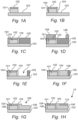
Figs. 1a-h are cross sections illustrating process flows according to some methods for forming an interconnection structure. -
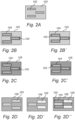
Figs. 2a-f' are top views illustrating process flows according to some methods for forming an interconnection structure. -
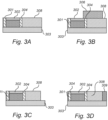
Figs. 3a-d are cross sections illustrating process flows according to some methods for forming an interconnection structure. -
Figs. 4a-c' are top views illustrating process flows according to some methods for forming an interconnection structure. - A method for forming an interconnection structure, suitable for instance for a semiconductor device, will now be described with reference to
Figs. 1a-h . - With reference to
figure 1a there is shown, in cross section, a portion of an intermediate structure or device. The structure may extend laterally or horizontally beyond the illustrated portion. The illustrated planes or layers extending through the structure are common to all the figures unless stated otherwise. It is noted that the relative dimensions of the shown elements, in particular the relative thickness of the layers, is merely schematic and may, for the purpose of illustrational clarity, differ from a physical structure. - The structure comprises an insulating
layer 103, a firstconductive metal line 101 and afirst mask layer 102. The insulatinglayer 103 may be formed of an electrically insulating material, typically a dielectric layer such as a layer of silicon oxide or some other conventional low-κ dielectric layer. For instance, the insulatinglayer 103 may be a layer stack which in addition to a low-κ dielectric layer comprises an interface layer and/or an oxide capping layer. The insulatinglayer 103 may for instance be deposited by chemical vapor deposition (CVD). - A
first metal line 101 may be formed by providing a conductive layer on the insulatinglayer 103 and thereafter etching the conductive layer, using thefirst mask layer 102 as an etch mask. Thefirst metal line 101 may be formed using a sequence of lithography and etching steps (a "litho-etch sequence"), for example including a dry etching process such as a reactive ion etch (RIE) or ion beam etching (IBE). - The conductive layer may be a metal layer, for instance a layer of ruthenium (Ru). Other examples of the conductive layer include a layer of molybdenum (Mo), tungsten (W), aluminum (Al) and cobalt (Co), and alloys thereof. Preferably, a metal may be used, which is suitable for patterning by means of metal etching. The conductive layer may be deposited by CVD or atomic layer deposition (ALD). The conductive layer may also be deposited by physical vapor deposition (PVD) or electroplated. The conductive layer may be a single metal of the aforementioned materials, or a multilayer combining two or more metals deposited with the same or different methods among the ones just cited.
- The
first mask layer 102 may for example be a hard mask composed of silicon oxide (SiO2), silicon nitride (SiN), silicon carbon nitride (SiCN or silicon carbide (SiC). It will however be appreciated that other materials could be used as well, such as spin-on oxide, and conductive materials which may be removed in later processing steps. Thefirst mask 102 may be used as an etch mask for forming the first set ofconductive lines 101 from the conductive layer. The firstconductive line 101 may be formed by a metal etch process, also referred to as a direct metal etch. - A litho-etch sequence may generally comprise forming a photoresist mask layer on the layer which will be patterned, i.e., the "target layer" (such as the conductive layer). A pattern (e.g. a pattern of openings, trenches or lines) may be lithographically defined in the photoresist layer and then transferred onto the target layer by etching while using the pattered photoresist layer as an etch mask. The photoresist layer may thereafter be stripped from the target layer. A litho-etch sequence may also comprise forming a lithographic mask layer stack (a "litho stack") on the target layer. The litho stack may comprise a patterning layer as a lower layer of the litho stack. The patterning layer may be an amorphous-carbon film, or some other conventional organic or non-organic patterning film allowing high-fidelity pattern transfer into the target layer in question. The litho stack may further comprise a photoresist layer and a set of transfer layers intermediate between the patterning layer and the photoresist layer. The set of intermediate layers may comprise, for instance, one or more anti-reflective coatings such as SiOC layers, SOG layers and optionally a planarization layer such as an organic spin-on layer (e.g. a SOC layer). A pattern may be lithographically defined in the photoresist layer and subsequently transferred into lower layers of the litho stack, in a number of etch steps, and subsequently into the patterning layer. The pattern transfer process may cause a partial consumption of the litho stack layer stack. For instance, the photoresist layer may be consumed during the transfer process. The litho-etch sequence may conclude by etching the target layer while using the patterned patterning layer as an etch mask. Any remaining layers of the litho stack may thereafter be stripped from the target layer.
- In
figure 1b , aspacer 104 has been formed on a side wall of a first end portion of the firstconductive line 101. The spacer may be formed by depositing a spacer layer followed by a litho-etch sequence to achieve the desired location and thickness of thespacer 104. The spacer may for example have a thickness of from 4 to 14 nm, such as from 6 to 12 nm, such as from 6 to 10 nm. Thespacer 104 may for instance be formed of a layer of a carbon-comprising material or a silicon-comprising material, such as amorphous carbon, polysilicon, amorphous silicon, silicon oxide, silicon nitride, or silicon carbide, which may be deposited for example by CVD or ALD. The deposition may be of an isotropic nature, resulting in a substantially conformal layer having the same thickness on surfaces in all directions. Alternatively, the deposition may be of a more anisotropic nature, in which the thickness of the resulting layer may vary in the horizontal and the vertical directions. In the structure illustrated infigure 1b any spacer material on horizontal surfaces has been etched or recessed, leaving thespacers 104 on the sidewalls of the first conductive line. It is thus understood that the spacer may be arranged at a side wall of a first end portion and a side wall of a second end portion of the firstconductive line 101. The spacers may in some examples be arranged further on side walls of the first conductive line to provide electrical insulation to neighbouring structures, such as other conductive lines. - The second
conductive line 108 may in some examples be formed in a damascene-style process, and in other examples by means of a direct metal etch similar to the one discussed above for the firstconductive line 101. In the following, an example of a damascene-style process will be discussed. - Hence,
figure 1c depicts an embodiment in which atrench layer 105 has been deposited on the intermediate structure infigure 1b . Thetrench layer 105 may comprise an electrically insulating material, typically a dielectric layer such as a layer of silicon oxide, another suitable oxide, or some other conventional low-κ dielectric material. In this particular embodiment, the intermediate structure has been planarized using a CMP process so as to provide a substantially planar surface. It is understood that the intermediate structure may be planarized by etching back the deposited trench layer. - In
figure 1d , athird mask layer 106 has been deposited on an intermediate structure offigure 1c . Thethird mask layer 106 has further been etched to expose a portion of theunderlying trench layer 105 accessible over the secondconductive line 108. - In
figure 1e , atrench 107 has been etched in thetrench layer 105 using thethird mask layer 106 as an etch mask. It is understood that thetrench layer 105 may differ from thespacer 104 with regard to etch selectivity. This advantageously allows for e.g. thetrench layer 105 to be etched while leaving thespacer 104 substantially intact. It will be appreciated that thetrench layer 105 further may differ from thefirst mask 102 with respect to etch selectivity, which may be particularly advantageous in case thefirst mask 102 is partly exposed by thethird mask layer 106. Thetrench 107 may thus be etched in a self-aligned fashion to the spacer. - Thereafter, the trench may be filled with a conductive material to form the second
conductive line 108 as illustrated infigure 1f . After the filling, excess material may be etched back or removed by a chemical-mechanical polishing (CMP) process. Thus, the secondconductive line 108 is formed, parallel to the firstconductive line 101, having a second end portion, wherein a side wall of the second end portion is arranged to abut the spacer, such that the first and thesecond metal line spacer 104. - In
figure 1g , arecess 109 has been formed in thesecond metal line 108, wherein therecess 109 extends along a portion of thesecond metal line 108. Further, asecond mask layer 110 has been formed in therecess 109, seefigure 1h . The recess may be laterally spaced apart from thespacer 104. Accordingly, a top portion of the secondconductive line 108 may be defined between thespacer 104 and thesecond mask layer 110. This portion may be referred to as a contacting portion and may be used for connecting the second conductive line to an upper interconnection level, for instance by means of a via connection. - Similar to the first conductive layer, the second conductive layer may comprise Ru, Mo, W, Al, and Co, as well as combinations thereof. Due to the damascene-style processing, it is appreciated that the second conductive layer may not necessarily be limited to materials that are possible to etch.
- In some embodiments, a TiN layer or TiN liner may be arranged under the first and/or second conductive lines for improving adhesion between the conductive line and the substrate. The TiN layer may cover the entire interface between the first and/or second conductive lines, or portions of the interface. The thickness of the TiN layer may for instance range from about 0.1 to about 2 nm.
-
Figures 2a-2f' depict top-views of the interconnection device and intermediate structures discussed above with reference tofigures 1a-f .Figure 2a corresponds tofigure 1a ,figures 2b and 2b' correspond tofigure 1b ,figures 2c and 2c' correspond tofigure 1c ,figures 2d, 2d' and 2d " correspond tofigure 1d ,figures 2e and 2e' correspond tofigure 1e , andfigures 2f and 2f' correspond tofigure 1f . - Thus,
figure 2a depicts a structure comprising an insulatinglayer 103 and a plurality of firstconductive metal lines 101, having afirst mask layer 102 arranged thereon.Figures 2b and 2b' depictspacers 104 formed on a side wall of a first end portion of each of the firstconductive lines 101.Figures 2c and 2c' depict an embodiment comprising atrench layer 105 deposited on the intermediate structure as depicted infigures 2b and 2b'. Figures 2d, 2d' and 2d " depict an embodiment comprising athird mask layer 106 deposited on an intermediate structure. Thethird mask layer 106 has further been patterned to expose a portion of theunderlying trench layer 105. Infigures 2e and 2e' trenches 107 have been etched in thetrench layer 105 using thethird mask layer 106 as an etch mask.Figures 2f and 2f' illustrates examples wherein the trenches have been filled with a conductive material to form a plurality of secondconductive lines 108. - In some embodiments, the plurality of first
conductive lines 101 are arranged separate from each other both in a direction orthogonal to the lines and in a lengthwise direction, seefigure 2a . The plurality of conductive lines may be provided with spacers to enclose each of the first conductive lines. Thus, the first conductive lines may be considered having a relaxed pitch.Trenches 107 may be etched in thetrench layer 105 using thethird mask layer 106 as an etch mask. Here, the third mask may comprise separate mask openings for each of the trenches, seeFigure 2d . - As depicted in
figure 2b' , the plurality of first conductive lines may be arranged with tighter pitch as compared tofigure 2a . The plurality of conductive lines may be provided with spacers to enclose each of the first conductive lines. In this example, the conductive lines may be arranged sufficiently close to each other to allow eachspacer 104 to at least partly abut a neighbouringspacer 104. Expressed differently, eachspacer 104 may be considered to be in contact with at least oneother spacer 104. This allows for a great relaxation in the lithography print using thethird mask layer 106, as illustrated infigure 2d ", as separate mask openings of thethird mask layer 106 are not necessary. Rather, one mask opening of thethird mask layer 106 may be provided and used for forming a plurality oftrenches 107 defined by the spacing between the neighbouringconductive lines 101. Alternatively, thethird mask layer 106 may be patterned with separate mask openings for each of the trenches, as illustrated in seefigure 2d' . - As an alternative to the above damascene-style processing, the second metal line may be formed in a direct etch process which will be described in the following with reference to
figures 3a-d . - Thus,
figures 3a-3d depict embodiments where a secondconductive line 308 has been formed by etching a second conductive layer arranged above the insulatinglayer 303, using athird mask layer 306 as an etch mask. The secondconductive line 308 may be arranged parallel to the firstconductive line 301, having a second end portion arranged to abut thespacer 304. Thus, the first and thesecond metal line spacer 304. It is understood that the steps preceding to what is depicted infigure 3a are described infigures 1a and 1b . It is understood that afirst mask layer 302 is arranged on the firstconductive line 301. - In
figure 3d aprotective layer 309 has been arranged at a sidewall of a third end portion of the second conductive line, wherein the third end portion is opposite to the second end portion. Theprotective layer 309 may comprise an insulating material. The insulating material may be an electrically insulating material, typically a dielectric material such as a layer of silicon oxide or some other conventional low-κ dielectric layer, to provide insulation to neighbouring structures such as additional conductive lines. -
Figures 4a-c' depict top-views of the interconnection structure and intermediate structures correspondingfigures 3a-d .Figures 4a, 4a', 4a " correspond tofigure 3b ,figures 4b, 4b' correspond tofigure 3c ,figures 4c, 4c' correspond tofigure 3d . -
Figures 4a, 4a', 4a " depict a plurality of first conductive lines arranged separate from each other both in a direction orthogonal to the lines and in a lengthwise direction. Here, a second conductive layer has been formed above the insulatinglayer 303, followed by athird mask layer 306 patterned to protect the portions of the second conductive layer from which the secondconductive lines 308 are to be formed.Figures 4b and 4b' show the second conductive layer after it has been etched through thethird mask layer 306 to form the secondconductive lines 308, andfigures 4c and 4c' show the interconnection structure after aprotective layer 309 has been arranged around the first and secondconductive lines - As indicated in the present figures, a plurality of first conductive lines 301 (in this example three) may be arranged on the insulating layer. Each of the first conductive lines may be arranged separated from each other, at a relatively relaxed pitch. In this example, the spacing between the first conductive lines may be sufficient to motivate the use of individual mask openings in the third mask layer when forming the second conductive lines.
- However, as depicted in
figures 4a', 4a ", the plurality of first conductive lines may be arranged with tighter pitch as compared tofigure 4a . As a consequence, neighbouringspacers 304 may at least partly abut each other. Expressed differently, eachspacer 304 may be considered to be in contact with at least oneother spacer 304. The relatively tight pitch between the first conductive lines allows for a relaxation in the lithography print defining thethird mask layer 306, as separate mask portions are not needed for individual lines - seefigure 4a ". Instead, thethird mask 306 may comprise a single block protecting all three conductive lines illustrated infigure 4a ". - In the above the inventive concept has mainly been described with reference to a limited number of examples. However, as is readily appreciated by a person skilled in the art, other examples than the ones disclosed above are equally possible within the scope of the inventive concept, as defined by the appended claims.
Claims (12)
- A method for forming an interconnection structure (10) for a semiconductor device, the method comprising:forming a conductive layer on an insulating layer (103);etching the conductive layer to form a first conductive line (101), using a first mask layer (102) as an etch mask;forming a spacer (104) on a side wall of a first end portion of the first conductive line;forming a second conductive line (108), parallel to the first conductive line, having a second end portion, wherein a side wall of the second end portion is arranged to abut the spacer, such that the first and the second metal line are extending along the same line and separated by the spacer;forming a recess (109) in the second metal line, the recess extending along a portion of the second metal line; andforming a second mask layer (110) in the recess.
- The method according to claim 1, wherein forming the second conductive line comprises:depositing a trench layer (105) above the insulating layer;etching a trench (107) in the trench layer; andfilling the trench with a conductive material to form the second conductive line.
- The method according to claim 1, wherein forming the second conductive line comprises:forming a second conductive layer above the insulating layer; andetching the second conductive layer to form the second conductive line, using a third mask layer (306) as an etch mask.
- The method according to claim 3, comprising:forming a protective layer (309) at a sidewall of a third end portion of the second conductive line, wherein the third end portion is opposite the second end portion.
- The method according to claim 3 or 4, wherein the first mask and the third mask differ with respect to etch selectivity.
- The method according to any one of the preceding claims, wherein the recess is laterally spaced apart from the spacer.
- The method according to any one of the preceding claims, wherein the first and the second mask differ with respect to etch selectivity.
- The method according to any of the preceding claims, wherein a top surface of the first mask layer and a top surface of the second mask layer are arranged at the same vertical level.
- The method according to any one of the preceding claims, wherein at least one of the first and second conductive lines is formed of at least one of Ru, Mo, W, Al and Co.
- The method according to any one of the preceding claims, wherein the first and second conducting lines consist of different conductive materials.
- The method according to any one of the preceding claims, wherein the first and second conducting lines consist of substantially the same conductive material.
- An interconnection structure for a semiconductor device, comprising:a first conductive line (101) and a second conductive line (108) arranged on an insulating layer (103);a spacer (104) separating the first and second conductive lines,wherein a side wall of a first end portion of the first conductive line and a side wall of a second end portion of the second conductive line abut the spacer, such that the first and second conductive lines are extending along the same line and separated by the spacer;a first mask layer (102) covering the first conductive line; anda second mask layer (110) arranged in a recess (109) in the second metal line, the recess extending along a portion of the second metal line.
Priority Applications (3)
| Application Number | Priority Date | Filing Date | Title |
|---|---|---|---|
| EP21210946.6A EP4187582A1 (en) | 2021-11-29 | 2021-11-29 | Interconnection structure for a semiconductor device |
| US18/053,636 US12451429B2 (en) | 2021-11-29 | 2022-11-08 | Interconnection structure for a semiconductor device |
| CN202211403548.1A CN116190308A (en) | 2021-11-29 | 2022-11-10 | Interconnect Structures for Semiconductor Devices |
Applications Claiming Priority (1)
| Application Number | Priority Date | Filing Date | Title |
|---|---|---|---|
| EP21210946.6A EP4187582A1 (en) | 2021-11-29 | 2021-11-29 | Interconnection structure for a semiconductor device |
Publications (1)
| Publication Number | Publication Date |
|---|---|
| EP4187582A1 true EP4187582A1 (en) | 2023-05-31 |
Family
ID=78819308
Family Applications (1)
| Application Number | Title | Priority Date | Filing Date |
|---|---|---|---|
| EP21210946.6A Pending EP4187582A1 (en) | 2021-11-29 | 2021-11-29 | Interconnection structure for a semiconductor device |
Country Status (3)
| Country | Link |
|---|---|
| US (1) | US12451429B2 (en) |
| EP (1) | EP4187582A1 (en) |
| CN (1) | CN116190308A (en) |
Citations (4)
| Publication number | Priority date | Publication date | Assignee | Title |
|---|---|---|---|---|
| WO2017171715A1 (en) * | 2016-03-28 | 2017-10-05 | Intel Corporation | Pitch division patterning approaches with increased overlay margin for back end of line (beol) interconnect fabrication and structures resulting therefrom |
| US20200357748A1 (en) * | 2019-05-10 | 2020-11-12 | International Business Machines Corporation | Forming self-aligned multi-metal interconnects |
| US20210082714A1 (en) * | 2019-09-13 | 2021-03-18 | International Business Machines Corporation | Back end of line structures with metal lines with alternating patterning and metallization schemes |
| US20210118732A1 (en) * | 2019-10-22 | 2021-04-22 | International Business Machines Corporation | Double patterning interconnect integration scheme with sav |
Family Cites Families (3)
| Publication number | Priority date | Publication date | Assignee | Title |
|---|---|---|---|---|
| US9324650B2 (en) * | 2014-08-15 | 2016-04-26 | International Business Machines Corporation | Interconnect structures with fully aligned vias |
| US10354912B2 (en) * | 2016-03-21 | 2019-07-16 | Qualcomm Incorporated | Forming self-aligned vertical interconnect accesses (VIAs) in interconnect structures for integrated circuits (ICs) |
| US12538785B2 (en) * | 2021-11-03 | 2026-01-27 | International Business Machines Corporation | Fully-aligned and dielectric damage-less top via interconnect structure |
-
2021
- 2021-11-29 EP EP21210946.6A patent/EP4187582A1/en active Pending
-
2022
- 2022-11-08 US US18/053,636 patent/US12451429B2/en active Active
- 2022-11-10 CN CN202211403548.1A patent/CN116190308A/en active Pending
Patent Citations (4)
| Publication number | Priority date | Publication date | Assignee | Title |
|---|---|---|---|---|
| WO2017171715A1 (en) * | 2016-03-28 | 2017-10-05 | Intel Corporation | Pitch division patterning approaches with increased overlay margin for back end of line (beol) interconnect fabrication and structures resulting therefrom |
| US20200357748A1 (en) * | 2019-05-10 | 2020-11-12 | International Business Machines Corporation | Forming self-aligned multi-metal interconnects |
| US20210082714A1 (en) * | 2019-09-13 | 2021-03-18 | International Business Machines Corporation | Back end of line structures with metal lines with alternating patterning and metallization schemes |
| US20210118732A1 (en) * | 2019-10-22 | 2021-04-22 | International Business Machines Corporation | Double patterning interconnect integration scheme with sav |
Also Published As
| Publication number | Publication date |
|---|---|
| US12451429B2 (en) | 2025-10-21 |
| US20230170300A1 (en) | 2023-06-01 |
| CN116190308A (en) | 2023-05-30 |
Similar Documents
| Publication | Publication Date | Title |
|---|---|---|
| US10170306B2 (en) | Method of double patterning lithography process using plurality of mandrels for integrated circuit applications | |
| KR20190087843A (en) | Semiconductor device | |
| US10147637B2 (en) | Methods for forming conductive paths and vias | |
| US12243771B2 (en) | Selective patterning of vias with hardmasks | |
| US20180102317A1 (en) | Interconnect structures with fully aligned vias | |
| KR20130115878A (en) | Method of manufacturing a contact structure | |
| US11127627B2 (en) | Method for forming an interconnection structure | |
| US9570397B1 (en) | Local interconnect structure including non-eroded contact via trenches | |
| US10593549B2 (en) | Method for defining patterns for conductive paths in a dielectric layer | |
| US20200194306A1 (en) | Self-aligned cuts in an interconnect structure | |
| US11894265B2 (en) | Top via with damascene line and via | |
| US10651076B2 (en) | Method for defining patterns for conductive paths in dielectric layer | |
| WO2024194704A1 (en) | Top via interconnect | |
| US7927990B2 (en) | Forming complimentary metal features using conformal insulator layer | |
| EP4145498A1 (en) | Staggered interconnection structure | |
| US12381116B2 (en) | Method of manufacturing an interconnection structure for a semiconductor device having a spacer separating first and second conductive lines | |
| US12451429B2 (en) | Interconnection structure for a semiconductor device | |
| US20070072334A1 (en) | Semiconductor fabrication process employing spacer defined vias | |
| TWI838721B (en) | Subtractive metal etch with improved isolation for beol interconnect and cross point | |
| US9837307B2 (en) | Semiconductor device and process | |
| US10395978B2 (en) | Method of patterning target layer | |
| EP3836198B1 (en) | A method for forming a via hole self-aligned with a metal block on a substrate | |
| EP3843130A1 (en) | A method for forming an interconnection structure | |
| CN114446770A (en) | Semiconductor structure and forming method thereof |
Legal Events
| Date | Code | Title | Description |
|---|---|---|---|
| PUAI | Public reference made under article 153(3) epc to a published international application that has entered the european phase |
Free format text: ORIGINAL CODE: 0009012 |
|
| STAA | Information on the status of an ep patent application or granted ep patent |
Free format text: STATUS: THE APPLICATION HAS BEEN PUBLISHED |
|
| AK | Designated contracting states |
Kind code of ref document: A1 Designated state(s): AL AT BE BG CH CY CZ DE DK EE ES FI FR GB GR HR HU IE IS IT LI LT LU LV MC MK MT NL NO PL PT RO RS SE SI SK SM TR |
|
| STAA | Information on the status of an ep patent application or granted ep patent |
Free format text: STATUS: REQUEST FOR EXAMINATION WAS MADE |
|
| 17P | Request for examination filed |
Effective date: 20231114 |
|
| RBV | Designated contracting states (corrected) |
Designated state(s): AL AT BE BG CH CY CZ DE DK EE ES FI FR GB GR HR HU IE IS IT LI LT LU LV MC MK MT NL NO PL PT RO RS SE SI SK SM TR |