EP4187239A1 - Electrode - Google Patents
Electrode Download PDFInfo
- Publication number
- EP4187239A1 EP4187239A1 EP21846785.0A EP21846785A EP4187239A1 EP 4187239 A1 EP4187239 A1 EP 4187239A1 EP 21846785 A EP21846785 A EP 21846785A EP 4187239 A1 EP4187239 A1 EP 4187239A1
- Authority
- EP
- European Patent Office
- Prior art keywords
- layer
- electrode
- metal
- oxide layer
- electrically conductive
- Prior art date
- Legal status (The legal status is an assumption and is not a legal conclusion. Google has not performed a legal analysis and makes no representation as to the accuracy of the status listed.)
- Pending
Links
Images



Classifications
-
- G—PHYSICS
- G01—MEASURING; TESTING
- G01N—INVESTIGATING OR ANALYSING MATERIALS BY DETERMINING THEIR CHEMICAL OR PHYSICAL PROPERTIES
- G01N27/00—Investigating or analysing materials by the use of electric, electrochemical, or magnetic means
- G01N27/26—Investigating or analysing materials by the use of electric, electrochemical, or magnetic means by investigating electrochemical variables; by using electrolysis or electrophoresis
- G01N27/28—Electrolytic cell components
- G01N27/30—Electrodes, e.g. test electrodes; Half-cells
- G01N27/308—Electrodes, e.g. test electrodes; Half-cells at least partially made of carbon
Definitions
- the present invention relates to an electrode.
- Patent Document 1 an electrode including a film substrate, a titanium thin film, and a carbon thin film in order in a thickness direction has been known (ref: for example, Patent Document 1 below).
- Patent Document 1 No. WO2016/013478
- the electrode may be immersed in an electrolytic solution for a long period of time.
- the electrode is required to suppress damage in the above-described case. That is to say, the electrode is required to have excellent electrolytic solution durability.
- the present invention provides an electrode having excellent electrolytic solution durability.
- the present invention (1) includes an electrode including a substrate film, an inorganic oxide layer, a metal underlying layer, and an electrically conductive carbon layer in order toward one side in a thickness direction.
- the present invention (2) includes the electrode described in (1), wherein the metal underlying layer is capable of forming carbide of carbon of the electrically conductive carbon layer.
- the present invention (3) includes the electrode described in (1) or (2), wherein the inorganic oxide layer is a metal oxide layer or a semi-metal oxide layer.
- the present invention (4) includes the electrode described in (3), wherein the metal oxide layer and the metal underlying layer contain the same metal element.
- the present invention (5) includes the electrode described in (4), wherein the metal element is titanium.
- the present invention (6) includes the electrode described in any one of (3) to (5), wherein the semi-metal oxide layer contains silicon dioxide.
- the present invention (7) includes the electrode described in any one of (1) to (6), wherein a thickness of the metal oxide layer is 5 nm or more.
- the present invention (8) includes the electrode described in any one of (1) to (7) being an electrode for electrochemical measurement.
- the electrode of the present invention has excellent electrolytic solution durability.
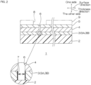
- FIGS. 1 to 2 One embodiment of an electrode of the present invention is described with reference to FIGS. 1 to 2 .
- an electrode 1 has a predetermined thickness.
- the electrode 1 has a film shape (including a sheet shape).
- the electrode 1 includes a substrate film 2, an inorganic oxide layer 3, a metal underlying layer 4, and an electrically conductive carbon layer 5 in order toward one side in a thickness direction.
- the electrode 1 includes only the substrate film 2, the inorganic oxide layer 3, the metal underlying layer 4, and the electrically conductive carbon layer 5.
- the substrate film 2 has a predetermined thickness.
- a material for the substrate film 2 include inorganic materials and organic materials. These may be used alone or in combination of two or more.
- the inorganic material include silicon and glass. These may be used alone or in combination of two or more.
- the organic material include resin materials.
- the resin material include polyester resins, acetate resins, polyether sulfone resins, polycarbonate resins, polyamide resins, polyimide resins, polyolefin resins, acrylic resins, polyvinyl chloride resins, polyvinylidene chloride resins, polystyrene resins, polyvinyl alcohol resins, polyarylate resins, and polyphenylene sulfide resins. These may be used alone or in combination of two or more.
- an organic material is used, more preferably, a polyester resin is used.
- the polyester resin include polyethylene terephthalate and polyethylene naphthalate.
- the polyester resin preferably, polyethylene terephthalate is used.
- Athickness of the substrate film 2 is not particularly limited.
- the thickness of the substrate film 2 is, for example, 2 ⁇ m or more, preferably 20 ⁇ m or more, and for example, 1000 ⁇ m or less, preferably 500 ⁇ m or less.
- the inorganic oxide layer 3 is disposed on one surface in the thickness direction of the substrate film 2. Specifically, the inorganic oxide layer 3 is in contact with the entire one surface in the thickness direction of the substrate film 2.
- the inorganic oxide layer 3 has a predetermined thickness.
- Examples of the inorganic oxide layer 3 include a metal oxide layer 3A and a semi-metal oxide layer 3B.
- the metal oxide layer 3A is passive. Specifically, the passivity is made of a metal oxide.
- the metal oxide include nickel oxide, cobalt oxide, chromium oxide, titanium oxide, aluminum oxide, tungsten oxide, molybdenum oxide, and composite oxide of these. These may be used alone or in combination of two or more.
- titanium oxide is used from the viewpoint of further improving electrolytic solution durability.
- the semi-metal oxide layer 3B is made of a semi-metal oxide.
- the semi-metal is not limited.
- Examples of the semi-metal include silicon, antimony, germanium, and bismuth.
- As the semi-metal preferably, silicon is used.
- Specific examples of the semi-metal oxide include silicon oxide, antimony oxide, germanium oxide, and bismuth oxide.
- examples of the semi-metal oxide include glass such as borosilicate glass.
- silicon oxide is used from the viewpoint of further improving the electrolytic solution durability.
- Examples of the silicon oxide include silicon dioxide (silica) and silicon monoxide, and preferably, silicon dioxide is used.
- the thickness of the inorganic oxide layer 3 is not particularly limited.
- the thickness of the inorganic oxide layer 3 is, for example, 1 nm or more, preferably 5 nm or more, and for example, 50 nm or less, preferably 25 nm or less.
- the inorganic oxide layer 3 When the thickness of the inorganic oxide layer 3 is the above-described lower limit or more, the inorganic oxide layer 3 has excellent uniformity over a plane direction.
- the plane direction is a direction perpendicular to the thickness direction. Therefore, the inorganic oxide layer 3 becomes a continuous film, and the effect of improving electrode durability can be expected.
- the inorganic oxide layer 3 when the thickness of the inorganic oxide layer 3 is the above-described upper limit or less, the inorganic oxide layer 3 (particularly, the metal oxide layer 3A) also has excellent electrical conductivity.
- the metal underlying layer 4 is disposed on one surface in the thickness direction of the inorganic oxide layer 3. Specifically, the metal underlying layer 4 is in contact with the entire one surface in the thickness direction of the inorganic oxide layer 3.
- the metal underlying layer 4 has a predetermined thickness.
- the material for the metal underlying layer 4 is a metal.
- the metal is preferably capable of forming carbide of carbon of the electrically conductive carbon layer 5 to be described next. That is, the metal is capable of reacting with carbon of the electrically conductive carbon layer 5 and forming carbide.
- examples of the metal include the group 2 elements and the group 4 elements to the group 14 elements in the periodic table, and alloys of these. These may be used alone or in combination of two or more.
- metal underlying layer 4 and the metal oxide layer 3A include, for example, the same metal element.
- the group 4 element is used, more preferably, titanium and zirconium are used, further more preferably, titanium is used.
- the metal oxide layer 3A and the metal underlying layer 4 contain titanium as an element. Since when the metal oxide layer 3A and the metal underlying layer 4 contain titanium, it is possible to improve adhesion between the metal oxide layer 3A and the metal underlying layer 4, which is advantageous.
- the material for the metal oxide layer 3A is titanium oxide.
- the material for the metal underlying layer 4 is titanium as a metal.
- the electrically conductive carbon layer 5 is disposed on one surface in the thickness direction of the metal underlying layer 4. Specifically, the electrically conductive carbon layer 5 is in contact with the entire one surface in the thickness direction of the metal underlying layer 4.
- the electrically conductive carbon layer 5 has a predetermined thickness.
- the material for the electrically conductive carbon layer 5 is carbon, and preferably, carbon having sp 2 bonding and sp 3 bonding is used.
- the carbon having sp 2 bonding and sp 3 bonding has a graphite-type structure and a diamond structure.
- a ratio (sp 3 /sp 3 +sp 2 ) of the number of sp 3 -bonded atoms to the sum of the number of sp 3 -bonded atoms and the number of sp 2 -bonded atoms is not particularly limited.
- the above-described ratio (sp 3 /sp 3 +sp 2 ) is, for example, 0.1 or more, preferably 0.2 or more, and for example, 0.9 or less, preferably, 0.5 or less.
- the ratio (sp 3 /sp 3 +sp 2 ) is calculated based on the peak strength of the sp 2 bonding and the peak strength of the sp 3 bonding in the spectrum obtained by measuring one surface in the thickness direction of the electrically conductive carbon layer 5 by X-ray photoelectron spectroscopy.
- a concentration ratio (O/C) of oxygen to carbon is not particularly limited.
- the above-described concentration ratio (O/C) is, for example, 0.15 or less, preferably 0.10 or less, and for example, above 0.00, 0.01 or more, 0.02 or more, furthermore 0.03 or more.
- a concentration ratio is calculated based on the peak area of C1s and the peak area of O1s in the spectrum obtained by measuring one surface in the thickness direction of the electrically conductive carbon layer 5 by the X-ray photoelectron spectroscopy.
- a surface resistance value on one surface in the thickness direction of the electrically conductive carbon layer 5 is not particularly limited.
- the surface resistance of the electrically conductive carbon layer 5 is, for example, 1.0 ⁇ 10 4 ⁇ / ⁇ or less, preferably 1.0 ⁇ 10 3 ⁇ / ⁇ or less.
- the surface resistance can be measured by a four-terminal method in conformity with JIS K 7194.
- the thickness of the electrically conductive carbon layer 5 is not particularly limited.
- the thickness of the electrically conductive carbon layer 5 is, for example, 5 nm or more, more preferably 10 nm or more, and for example, 200 nm or less, more preferably 100 nm or less.
- the thickness of the electrically conductive carbon layer 5 is calculated by measurement of X-ray reflectance.
- a carbide layer (not shown) is formed at the interface between the electrically conductive carbon layer 5 and the metal underlying layer 4.
- the carbide layer consists of a carbide which is a compound of the metal of the metal underlying layer 4 and the carbon of the electrically conductive carbon layer 5.
- the adhesive force between the electrically conductive carbon layer 5 and the metal underlying layer 4 is improved by the carbide layer.
- the electrode 1 includes the substrate film 2, the inorganic oxide layer 3, the metal underlying layer 4, the carbide layer which is not shown, and the electrically conductive carbon layer 5 in order toward one side in the thickness direction.
- the substrate film 2 is prepared.
- the inorganic oxide layer 3, the metal underlying layer 4, and the electrically conductive carbon layer 5 are formed in order on one side in the thickness direction of the substrate film 2.
- Examples of a method for forming the inorganic oxide layer 3 include a dry method and a wet method.
- a dry method is used.
- Examples of the dry method include a PVD method (physical vapor deposition method) and a CVD method (chemical vapor deposition method).
- a PVD method is used.
- Examples of the PVD method include a sputtering method, a vacuum deposition method, a laser deposition method, and an ion plating method (arc deposition method).
- a sputtering method is used. The sputtering method is not particularly limited.
- Examples of the sputtering method include an unbalanced magnetron sputtering method (UBM sputtering method), a large power pulse sputtering method, an electron cyclotron resonance sputtering method, an RF sputtering method, a DC sputtering method (DC magnetron sputtering method), a DC pulse sputtering method, and an ion beam sputtering method.
- UBM sputtering method unbalanced magnetron sputtering method
- a large power pulse sputtering method an electron cyclotron resonance sputtering method
- an RF sputtering method a DC sputtering method (DC magnetron sputtering method)
- DC magnetron sputtering method DC pulse sputtering method
- ion beam sputtering method ion beam sputtering method
- a sputtering gas containing oxygen and an inert gas, and a target made of an inorganic material are used.
- An example of the inert gas includes argon.
- a flow ratio of oxygen to the total flow rate of the sputtering gas is, for example, 0.01 or more, preferably 0.05, and for example, below 0.5, preferably 0.2 or less.
- Examples of the inorganic material include metals and semi-metals.
- metal includes a metal element which forms a metal oxide.
- the metal include nickel, cobalt, chromium, titanium, aluminum, tungsten, molybdenum, and alloys of these.
- titanium is used from the viewpoint of chemical stability.
- An example of the semi-metal includes the above-described semi-metal, and preferably, silicon is used.
- An example of the method for forming the metal underlying layer 4 includes the same method as the above-described forming method of the inorganic oxide layer 3. However, when the metal underlying layer 4 is formed by a sputtering method, a sputtering gas which contains only an inert gas without containing oxygen is used.
- the target material preferably, the same target material as that used in forming the metal oxide layer 3A is used, more preferably, titanium is used.
- the target material preferably, the same target material as that used in forming the metal oxide layer 3A is used, more preferably, titanium is used.
- titanium is used in the formation of the metal oxide layer 3A and the formation of the metal underlying layer 4, since the target made of titanium can be common, it is easy to design a production facility.
- An example of the method for forming the electrically conductive carbon layer 5 includes the same method as the above-described forming method of the inorganic oxide layer 3. However, when the electrically conductive carbon layer 5 is formed by the sputtering method, the sputtering gas which contains only the inert gas without containing the oxygen is used. When the electrically conductive carbon layer 5 is formed by the sputtering method, as the target material, for example, carbon is used, preferably, sintered carbon is used. Thereafter, if necessary, the electrically conductive carbon layer 5 may be subjected to surface treatment.
- the electrode 1 since the electrode 1 includes the substrate film 2, the inorganic oxide layer 3, the metal underlying layer 4, and the electrically conductive carbon layer 5 in order toward one side in the thickness direction, it has excellent electrolytic solution durability.
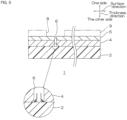
- the pinhole 6 is a hole penetrating the inorganic oxide layer 3, the metal underlying layer 4, and the electrically conductive carbon layer 5 in the thickness direction.
- a foreign matter dust
- the inorganic oxide layer 3, the metal underlying layer 4, and the electrically conductive carbon layer 5 are formed on one side in the thickness direction of the foreign matter.
- the electrolytic solution infiltrates the interface between the metal underlying layer 4 and the substrate film 2 from the pinhole 6. Therefore, the metal underlying layer 4 is easily peeled from one surface in the thickness direction of the substrate film 2. Therefore, the electrode 1 of FIG. 3 has insufficient electrolytic solution durability.
- the electrolytic solution durability means that the electrically conductive carbon layer 5 is hardly damaged when the electrode 1 is immersed in the electrolytic solution for a long period of time.
- the electrolytic solution durability means that the electrically conductive carbon layer 5 is hardly damaged when the electrode 1 is immersed in the electrolytic solution for, for example, 5 days or more, furthermore 10 days or more, furthermore 15 days or more, furthermore 20 days or more.
- the metal underlying layer 4 is in contact with one surface in the thickness direction of the substrate film 2. Therefore, as shown by the arrows of FIG. 4 , the electrolytic solution infiltrates the interface between the metal underlying layer 4 and the substrate film 2 from the pinhole 6.
- the inorganic oxide layer 3 is provided between the metal underlying layer 4 and the substrate film 2. Therefore, it is possible to suppress the infiltration of the electrolytic solution between the metal underlying layer 4 and the substrate film 2 by the inorganic oxide layer 3.
- the inorganic oxide layer 3 can function as a barrier layer against the electrolytic solution.
- an inner peripheral surface 7 facing the pinhole 6 becomes a stopper portion.
- the electrolytic solution infiltrates the interface between the electrically conductive carbon layer 5 and the metal underlying layer 4, and the peeling of the electrically conductive carbon layer 5 from the metal underlying layer 4 occurs.
- the carbide layer is formed at the interface between the electrically conductive carbon layer 5 and the metal underlying layer 4. Therefore, the adhesive force between the electrically conductive carbon layer 5 and the metal underlying layer 4 is improved, and it is possible to suppress the above-described infiltration. Therefore, it is also possible to suppress the peeling of the electrically conductive carbon layer 5 from the metal underlying layer 4.
- the metal oxide layer 3A and the metal underlying layer 4 are the same metal element, it is possible to improve the adhesion between the metal oxide layer 3A and the metal underlying layer 4. Furthermore, since the metal oxide layer 3A and the metal underlying layer 4 can use the target made of the same metal element, it is possible to use a common film forming chamber. Therefore, it is possible to produce the electrode 1 by a compact production facility.
- the chemical stability of the electrode 1 is excellent. Furthermore, in the formation of the metal oxide layer 3A and in the formation of the metal underlying layer 4, since the target made of titanium is common, it is easy to design the production facility.
- the inorganic oxide layer 3 is the semi-metal oxide layer 3B, therefore, it is possible to effectively suppress the infiltration of the electrolytic solution between the metal underlying layer 4 and the substrate film 2 by the semi-metal oxide layer 3B. Therefore, the electrode 1 including the semi-metal oxide layer 3B has excellent electrolytic solution durability.
- the thickness of the inorganic oxide layer 3 is 5 nm or more, the uniformity of the inorganic oxide layer 3 over the plane direction is excellent.
- the application of the electrode 1 is not particularly limited.
- Examples of the application of the electrode 1 include electrodes for electrochemical measurement.
- the electrode 1 is provided in an electrochemical measurement system as a working electrode. Examples
- the substrate film 2 made of polyethylene terephthalate and having a thickness of 50 ⁇ m was prepared.
- the metal oxide layer 3A (the inorganic oxide layer 3) made of titanium oxide was formed on one surface in the thickness direction of the substrate film 2 using a magnetron sputtering method.
- the conditions of the magnetron sputtering method were as follows.
- the metal underlying layer 4 made of titanium was formed on one surface in the thickness direction of the metal oxide layer 3A using the magnetron sputtering method.
- the conditions of the magnetron sputtering method were as follows.
- the electrically conductive carbon layer 5 was formed on one surface in the thickness direction of the metal underlying layer 4 by a DC pulse sputtering method.
- the conditions of the DC pulse sputtering method were as follows.
- the surface resistance of the electrically conductive carbon layer 5 was 130 ⁇ / ⁇ .
- the ratio (sp 3 /sp 3 +sp 2 ) in the electrically conductive carbon layer 5 was 0.35.
- the concentration ratio (O/C) of oxygen to carbon was 0.06.
- the thickness of the electrically conductive carbon layer 5 was 30 nm.
- the electrode 1 including the substrate film 2, the metal oxide layer 3A, the metal underlying layer 4, and the electrically conductive carbon layer 5 in order toward one side in the thickness direction was produced.
- the process was carried out in the same manner as in Example 1, except that the thickness of the metal oxide layer 3A was changed to 2 nm.
- the process was carried out in the same manner as in Example 1, except that the semi-metal oxide layer 3B was formed instead of the metal oxide layer 3A. That is, the semi-metal oxide layer 3B made of silicon dioxide (the inorganic oxide layer 3) was formed on one surface in the thickness direction of the substrate film 2 by a magnetron sputtering method.
- the conditions of the magnetron sputtering method were as follows.
- the process was carried out in the same manner as in Example 1, except that the thickness of the semi-metal oxide layer 3B was changed to 5 nm.
- the process was carried out in the same manner as in Example 1, except that the metal oxide layer 3A was not formed. That is, as shown in FIG. 3 , the electrode 1 included the substrate film 2, the metal underlying layer 4, and the electrically conductive carbon layer 5 in order toward one side in the thickness direction.
- the process was carried out in the same manner as in Example 1, except that the order of forming the metal oxide layer 3A and the metal underlying layer 4 was replaced. That is, as shown in FIG. 4 , the electrode 1 included the substrate film 2, the metal underlying layer 4, the metal oxide layer 3A, and the electrically conductive carbon layer 5 in order toward one side in the thickness direction.
- an insulating tape 9 was attached to one surface in the thickness direction of the electrically conductive carbon layer 5.
- the insulating tape 9 had an opening portion 8 having a diameter of 2 mm.
- the electrode 1 and the insulating tape 9 were immersed in 0.1 M of nitric acid solution for 56 days.
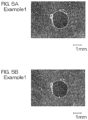
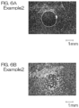
- FIGS. 5A to 8B show Example 1 to Comparative Example 2, respectively.
- FIG. 5A is the electrode 1 before the immersion in Example 1.
- FIG. 5B is the electrode 1 after the immersion in Example 1.
- FIGS. 6A to 8B are the same as the above-described FIGS. 5A to 5B .
- the electrolytic solution durability was evaluated from the OM image after the immersion based on the following criteria.
- a potential window of each of the electrodes 1 of Examples and Comparative Examples was measured using a potentiostat. Thus, the electrode properties of the electrode 1 were evaluated.
- the potential window means a voltage range in which no current flows even when a voltage is applied, and the wider the range, the more excellent the electrode properties of the electrode 1.
- An electrochemical measurement system including the electrode 1 as a working electrode was constructed.
- the electrochemical measurement system included an Ag/AgCl electrode as a reference electrode and a Pt electrode as a counter electrode.
- the electrode 1 was immersed in 0.1 M of sulfuric acid solution. Subsequently, an electric potential was swept with respect to the electrode 1, and the width of the electric potential when reaching 500 ⁇ A/cm 2 was defined as a potential window.
- FIG. 1 Electrically Conductive Carbon Semi-Metal Oxide Layer Silicon Dioxide 10 Excellent 3.7 Layer/Metal Underlying Layer/Inorganic Oxide Layer/Substrate Film Ex. 4
- FIGS. 1 , 2 Electrically Conductive Carbon Semi-Metal Oxide Layer Silicon Dioxide 5 Excellent 3.7 Layer/Metal Underlying Layer/Inorganic Oxide Layer/Substrate Film Comparative Ex. 1
- FIG. 3 Electrically Conductive Carbon Metal Oxide Layer Titanium Oxide 5 Bad 3.7 Layer/Inorganic Oxide Layer/Metal Underlying Layer/Substrate Film Comparative Ex. 2
- FIG. 4 Electrically Conductive Carbon Metal Oxide Layer Titanium Oxide - Bad 3.7 Layer/Inorganic Oxide Layer/Substrate Film
- the electrode of the present invention is used, for example, in electrochemical measurement.
Landscapes
- Chemical & Material Sciences (AREA)
- Life Sciences & Earth Sciences (AREA)
- Health & Medical Sciences (AREA)
- Biochemistry (AREA)
- General Physics & Mathematics (AREA)
- Electrochemistry (AREA)
- Physics & Mathematics (AREA)
- Analytical Chemistry (AREA)
- Molecular Biology (AREA)
- General Health & Medical Sciences (AREA)
- Chemical Kinetics & Catalysis (AREA)
- Immunology (AREA)
- Pathology (AREA)
- Hybrid Cells (AREA)
- Fuel Cell (AREA)
- Electrodes For Compound Or Non-Metal Manufacture (AREA)
- Battery Electrode And Active Subsutance (AREA)
- Laminated Bodies (AREA)
Abstract
Description
- The present invention relates to an electrode.
- Conventionally, an electrode including a film substrate, a titanium thin film, and a carbon thin film in order in a thickness direction has been known (ref: for example,
Patent Document 1 below). - In the electrode described in
Patent Document 1, chemical stability in a short time is also improved, while electrical conductivity is improved by the titanium thin film. - Patent Document 1: No.
WO2016/013478 - Thus, the electrode may be immersed in an electrolytic solution for a long period of time. The electrode is required to suppress damage in the above-described case. That is to say, the electrode is required to have excellent electrolytic solution durability.
- However, there is a problem that the electrode described in
Patent Document 1 does not have the above-described excellent electrolytic solution durability. - The present invention provides an electrode having excellent electrolytic solution durability.
- The present invention (1) includes an electrode including a substrate film, an inorganic oxide layer, a metal underlying layer, and an electrically conductive carbon layer in order toward one side in a thickness direction.
- The present invention (2) includes the electrode described in (1), wherein the metal underlying layer is capable of forming carbide of carbon of the electrically conductive carbon layer.
- The present invention (3) includes the electrode described in (1) or (2), wherein the inorganic oxide layer is a metal oxide layer or a semi-metal oxide layer.
- The present invention (4) includes the electrode described in (3), wherein the metal oxide layer and the metal underlying layer contain the same metal element.
- The present invention (5) includes the electrode described in (4), wherein the metal element is titanium.
- The present invention (6) includes the electrode described in any one of (3) to (5), wherein the semi-metal oxide layer contains silicon dioxide.
- The present invention (7) includes the electrode described in any one of (1) to (6), wherein a thickness of the metal oxide layer is 5 nm or more.
- The present invention (8) includes the electrode described in any one of (1) to (7) being an electrode for electrochemical measurement.
- The electrode of the present invention has excellent electrolytic solution durability.
-
-
FIG. 1 shows a cross-sectional view of one embodiment of an electrode of the present invention. -
FIG. 2 shows a cross-sectional view of an electrode in which a pinhole is formed. -
FIG. 3 shows a cross-sectional view of an electrode of Comparative Example 1. -
FIG. 4 shows a cross-sectional view of an electrode of Comparative Example 2. -
FIGS. 5A to 5B show an OM image of an electrode of Example 1:-
FIG. 5A illustrating the electrode before being immersed in an electrolytic solution and -
FIG. 5B illustrating the electrode after being immersed in the electrolytic solution.
-
-
FIGS. 6A to 6B show an OM image of an electrode of Example 2:-
FIG. 6A illustrating the electrode before being immersed in an electrolytic solution and -
FIG. 6B illustrating the electrode after being immersed in the electrolytic solution.
-
-
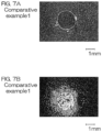
FIGS. 7A to 7B show an OM image of an electrode of Comparative Example 1:-
FIG. 7A illustrating the electrode before being immersed in an electrolytic solution and -
FIG. 7B illustrating the electrode after being immersed in the electrolytic solution.
-
-
FIGS. 8A to 8B show an OM image of an electrode of Comparative Example 2:-
FIG. 8A illustrating the electrode before being immersed in an electrolytic solution and -
FIG. 8B illustrating the electrode after being immersed in the electrolytic solution.
-
- One embodiment of an electrode of the present invention is described with reference to
FIGS. 1 to 2 . - As shown in
FIG. 1 , anelectrode 1 has a predetermined thickness. Theelectrode 1 has a film shape (including a sheet shape). Theelectrode 1 includes asubstrate film 2, aninorganic oxide layer 3, a metal underlyinglayer 4, and an electricallyconductive carbon layer 5 in order toward one side in a thickness direction. Specifically, theelectrode 1 includes only thesubstrate film 2, theinorganic oxide layer 3, the metal underlyinglayer 4, and the electricallyconductive carbon layer 5. - The
substrate film 2 has a predetermined thickness. Examples of a material for thesubstrate film 2 include inorganic materials and organic materials. These may be used alone or in combination of two or more. Examples of the inorganic material include silicon and glass. These may be used alone or in combination of two or more. Examples of the organic material include resin materials. Examples of the resin material include polyester resins, acetate resins, polyether sulfone resins, polycarbonate resins, polyamide resins, polyimide resins, polyolefin resins, acrylic resins, polyvinyl chloride resins, polyvinylidene chloride resins, polystyrene resins, polyvinyl alcohol resins, polyarylate resins, and polyphenylene sulfide resins. These may be used alone or in combination of two or more. - As the material for the
substrate film 2, preferably, an organic material is used, more preferably, a polyester resin is used. Specific examples of the polyester resin include polyethylene terephthalate and polyethylene naphthalate. As the polyester resin, preferably, polyethylene terephthalate is used. - Athickness of the
substrate film 2 is not particularly limited. The thickness of thesubstrate film 2 is, for example, 2 µm or more, preferably 20 µm or more, and for example, 1000 µm or less, preferably 500 µm or less. - The
inorganic oxide layer 3 is disposed on one surface in the thickness direction of thesubstrate film 2. Specifically, theinorganic oxide layer 3 is in contact with the entire one surface in the thickness direction of thesubstrate film 2. Theinorganic oxide layer 3 has a predetermined thickness. - Examples of the
inorganic oxide layer 3 include ametal oxide layer 3A and asemi-metal oxide layer 3B. - The
metal oxide layer 3A is passive. Specifically, the passivity is made of a metal oxide. Examples of the metal oxide include nickel oxide, cobalt oxide, chromium oxide, titanium oxide, aluminum oxide, tungsten oxide, molybdenum oxide, and composite oxide of these. These may be used alone or in combination of two or more. Preferably, titanium oxide is used from the viewpoint of further improving electrolytic solution durability. - The
semi-metal oxide layer 3B is made of a semi-metal oxide. The semi-metal is not limited. Examples of the semi-metal include silicon, antimony, germanium, and bismuth. As the semi-metal, preferably, silicon is used. Specific examples of the semi-metal oxide include silicon oxide, antimony oxide, germanium oxide, and bismuth oxide. Further, examples of the semi-metal oxide include glass such as borosilicate glass. As the semi-metal oxide, preferably, silicon oxide is used from the viewpoint of further improving the electrolytic solution durability. Examples of the silicon oxide include silicon dioxide (silica) and silicon monoxide, and preferably, silicon dioxide is used. - The thickness of the
inorganic oxide layer 3 is not particularly limited. The thickness of theinorganic oxide layer 3 is, for example, 1 nm or more, preferably 5 nm or more, and for example, 50 nm or less, preferably 25 nm or less. - When the thickness of the
inorganic oxide layer 3 is the above-described lower limit or more, theinorganic oxide layer 3 has excellent uniformity over a plane direction. The plane direction is a direction perpendicular to the thickness direction. Therefore, theinorganic oxide layer 3 becomes a continuous film, and the effect of improving electrode durability can be expected. - On the other hand, when the thickness of the
inorganic oxide layer 3 is the above-described upper limit or less, the inorganic oxide layer 3 (particularly, themetal oxide layer 3A) also has excellent electrical conductivity. - The metal
underlying layer 4 is disposed on one surface in the thickness direction of theinorganic oxide layer 3. Specifically, the metalunderlying layer 4 is in contact with the entire one surface in the thickness direction of theinorganic oxide layer 3. The metalunderlying layer 4 has a predetermined thickness. - The material for the metal
underlying layer 4 is a metal. The metal is preferably capable of forming carbide of carbon of the electricallyconductive carbon layer 5 to be described next. That is, the metal is capable of reacting with carbon of the electricallyconductive carbon layer 5 and forming carbide. Specifically, examples of the metal include thegroup 2 elements and thegroup 4 elements to the group 14 elements in the periodic table, and alloys of these. These may be used alone or in combination of two or more. - Further, the metal
underlying layer 4 and themetal oxide layer 3A include, for example, the same metal element. - As the metal for the material of the metal
underlying layer 4, from the viewpoint of ensuring chemical stability of the electricallyconductive carbon layer 5, preferably, thegroup 4 element is used, more preferably, titanium and zirconium are used, further more preferably, titanium is used. - Particularly preferably, the
metal oxide layer 3A and the metalunderlying layer 4 contain titanium as an element. Since when themetal oxide layer 3A and the metalunderlying layer 4 contain titanium, it is possible to improve adhesion between themetal oxide layer 3A and the metalunderlying layer 4, which is advantageous. When themetal oxide layer 3A contains titanium, the material for themetal oxide layer 3A is titanium oxide. The material for the metalunderlying layer 4 is titanium as a metal. - The electrically
conductive carbon layer 5 is disposed on one surface in the thickness direction of the metalunderlying layer 4. Specifically, the electricallyconductive carbon layer 5 is in contact with the entire one surface in the thickness direction of the metalunderlying layer 4. The electricallyconductive carbon layer 5 has a predetermined thickness. - The material for the electrically
conductive carbon layer 5 is carbon, and preferably, carbon having sp2 bonding and sp3 bonding is used. The carbon having sp2 bonding and sp3 bonding has a graphite-type structure and a diamond structure. A ratio (sp3/sp3+sp2) of the number of sp3-bonded atoms to the sum of the number of sp3-bonded atoms and the number of sp2-bonded atoms is not particularly limited. The above-described ratio (sp3/sp3+sp2) is, for example, 0.1 or more, preferably 0.2 or more, and for example, 0.9 or less, preferably, 0.5 or less. The ratio (sp3/sp3+sp2) is calculated based on the peak strength of the sp2 bonding and the peak strength of the sp3 bonding in the spectrum obtained by measuring one surface in the thickness direction of the electricallyconductive carbon layer 5 by X-ray photoelectron spectroscopy. - In one surface in the thickness direction of the electrically
conductive carbon layer 5, a concentration ratio (O/C) of oxygen to carbon is not particularly limited. The above-described concentration ratio (O/C) is, for example, 0.15 or less, preferably 0.10 or less, and for example, above 0.00, 0.01 or more, 0.02 or more, furthermore 0.03 or more. A concentration ratio is calculated based on the peak area of C1s and the peak area of O1s in the spectrum obtained by measuring one surface in the thickness direction of the electricallyconductive carbon layer 5 by the X-ray photoelectron spectroscopy. - A surface resistance value on one surface in the thickness direction of the electrically
conductive carbon layer 5 is not particularly limited. The surface resistance of the electricallyconductive carbon layer 5 is, for example, 1.0×10⁴ Ω/□ or less, preferably 1.0×10³ Ω/□ or less. The surface resistance can be measured by a four-terminal method in conformity with JIS K 7194. - The thickness of the electrically
conductive carbon layer 5 is not particularly limited. The thickness of the electricallyconductive carbon layer 5 is, for example, 5 nm or more, more preferably 10 nm or more, and for example, 200 nm or less, more preferably 100 nm or less. The thickness of the electricallyconductive carbon layer 5 is calculated by measurement of X-ray reflectance. - Further, preferably, a carbide layer (not shown) is formed at the interface between the electrically
conductive carbon layer 5 and the metalunderlying layer 4. The carbide layer consists of a carbide which is a compound of the metal of the metalunderlying layer 4 and the carbon of the electricallyconductive carbon layer 5. The adhesive force between the electricallyconductive carbon layer 5 and the metalunderlying layer 4 is improved by the carbide layer. In this case, theelectrode 1 includes thesubstrate film 2, theinorganic oxide layer 3, the metalunderlying layer 4, the carbide layer which is not shown, and the electricallyconductive carbon layer 5 in order toward one side in the thickness direction. - Next, a method for producing the
electrode 1 is described. First, thesubstrate film 2 is prepared. Next, theinorganic oxide layer 3, the metalunderlying layer 4, and the electricallyconductive carbon layer 5 are formed in order on one side in the thickness direction of thesubstrate film 2. - Examples of a method for forming the
inorganic oxide layer 3 include a dry method and a wet method. Preferably, a dry method is used. Examples of the dry method include a PVD method (physical vapor deposition method) and a CVD method (chemical vapor deposition method). As the dry method, preferably, a PVD method is used. Examples of the PVD method include a sputtering method, a vacuum deposition method, a laser deposition method, and an ion plating method (arc deposition method). As the PVD method, preferably, a sputtering method is used. The sputtering method is not particularly limited. Examples of the sputtering method include an unbalanced magnetron sputtering method (UBM sputtering method), a large power pulse sputtering method, an electron cyclotron resonance sputtering method, an RF sputtering method, a DC sputtering method (DC magnetron sputtering method), a DC pulse sputtering method, and an ion beam sputtering method. - Further, in the sputtering method, for example, a sputtering gas containing oxygen and an inert gas, and a target made of an inorganic material are used.
- An example of the inert gas includes argon. A flow ratio of oxygen to the total flow rate of the sputtering gas is, for example, 0.01 or more, preferably 0.05, and for example, below 0.5, preferably 0.2 or less.
- Examples of the inorganic material include metals and semi-metals.
- An example of the metal includes a metal element which forms a metal oxide. Examples of the metal include nickel, cobalt, chromium, titanium, aluminum, tungsten, molybdenum, and alloys of these. Preferably, titanium is used from the viewpoint of chemical stability.
- An example of the semi-metal includes the above-described semi-metal, and preferably, silicon is used.
- An example of the method for forming the metal
underlying layer 4 includes the same method as the above-described forming method of theinorganic oxide layer 3. However, when the metalunderlying layer 4 is formed by a sputtering method, a sputtering gas which contains only an inert gas without containing oxygen is used. - Further, as the target material, preferably, the same target material as that used in forming the
metal oxide layer 3A is used, more preferably, titanium is used. In the formation of themetal oxide layer 3A and the formation of the metalunderlying layer 4, since the target made of titanium can be common, it is easy to design a production facility. - An example of the method for forming the electrically
conductive carbon layer 5 includes the same method as the above-described forming method of theinorganic oxide layer 3. However, when the electricallyconductive carbon layer 5 is formed by the sputtering method, the sputtering gas which contains only the inert gas without containing the oxygen is used. When the electricallyconductive carbon layer 5 is formed by the sputtering method, as the target material, for example, carbon is used, preferably, sintered carbon is used. Thereafter, if necessary, the electricallyconductive carbon layer 5 may be subjected to surface treatment. - Then, since the
electrode 1 includes thesubstrate film 2, theinorganic oxide layer 3, the metalunderlying layer 4, and the electricallyconductive carbon layer 5 in order toward one side in the thickness direction, it has excellent electrolytic solution durability. - However, as shown in
FIG. 2 , there is a case where apinhole 6 is inevitably formed in theelectrode 1 due to its production. Thepinhole 6 is a hole penetrating theinorganic oxide layer 3, the metalunderlying layer 4, and the electricallyconductive carbon layer 5 in the thickness direction. For example, when a foreign matter (dust) is inevitably laminated (deposited) on one surface in the thickness direction of thesubstrate film 2 during transportation of thesubstrate film 2, theinorganic oxide layer 3, the metalunderlying layer 4, and the electricallyconductive carbon layer 5 are formed on one side in the thickness direction of the foreign matter. Since the adhesive force between the foreign matter and thesubstrate film 2 is significantly low, when the foreign matter is detached from one surface in the thickness direction of thesubstrate film 2, a portion corresponding to theinorganic oxide layer 3, the metalunderlying layer 4, and the electricallyconductive carbon layer 5 is also detached. Thus, the above-describedpinhole 6 is inevitably formed. - Then, when the
electrode 1 is immersed in a corrosive electrolytic solution, the electrolytic solution fills thepinhole 6. - However, as shown in
FIG. 3 , as inPatent Document 1, in theelectrode 1 without including theinorganic oxide layer 3, as shown by thick line arrows, the electrolytic solution infiltrates the interface between the metalunderlying layer 4 and thesubstrate film 2 from thepinhole 6. Therefore, the metalunderlying layer 4 is easily peeled from one surface in the thickness direction of thesubstrate film 2. Therefore, theelectrode 1 ofFIG. 3 has insufficient electrolytic solution durability. - In the present application, the electrolytic solution durability means that the electrically
conductive carbon layer 5 is hardly damaged when theelectrode 1 is immersed in the electrolytic solution for a long period of time. Specifically, the electrolytic solution durability means that the electricallyconductive carbon layer 5 is hardly damaged when theelectrode 1 is immersed in the electrolytic solution for, for example, 5 days or more, furthermore 10 days or more, furthermore 15 days or more, furthermore 20 days or more. - Further, as shown in
FIG. 4 , even in a layer configuration of replacing the formation order of theinorganic oxide layer 3 and the metalunderlying layer 4, the metalunderlying layer 4 is in contact with one surface in the thickness direction of thesubstrate film 2. Therefore, as shown by the arrows ofFIG. 4 , the electrolytic solution infiltrates the interface between the metalunderlying layer 4 and thesubstrate film 2 from thepinhole 6. - However, in the present embodiment, as shown in
FIG. 2 , even when the electrolytic solution fills thepinhole 6, theinorganic oxide layer 3 is provided between the metalunderlying layer 4 and thesubstrate film 2. Therefore, it is possible to suppress the infiltration of the electrolytic solution between the metalunderlying layer 4 and thesubstrate film 2 by theinorganic oxide layer 3. In other words, theinorganic oxide layer 3 can function as a barrier layer against the electrolytic solution. Specifically, in theinorganic oxide layer 3, an innerperipheral surface 7 facing thepinhole 6 becomes a stopper portion. - On the other hand, it is concerned that the electrolytic solution infiltrates the interface between the electrically
conductive carbon layer 5 and the metalunderlying layer 4, and the peeling of the electricallyconductive carbon layer 5 from the metalunderlying layer 4 occurs. However, in the present embodiment, the carbide layer is formed at the interface between the electricallyconductive carbon layer 5 and the metalunderlying layer 4. Therefore, the adhesive force between the electricallyconductive carbon layer 5 and the metalunderlying layer 4 is improved, and it is possible to suppress the above-described infiltration. Therefore, it is also possible to suppress the peeling of the electricallyconductive carbon layer 5 from the metalunderlying layer 4. - Further, when the
metal oxide layer 3A and the metalunderlying layer 4 are the same metal element, it is possible to improve the adhesion between themetal oxide layer 3A and the metalunderlying layer 4. Furthermore, since themetal oxide layer 3A and the metalunderlying layer 4 can use the target made of the same metal element, it is possible to use a common film forming chamber. Therefore, it is possible to produce theelectrode 1 by a compact production facility. - More specifically, when both the
metal oxide layer 3A and the metalunderlying layer 4 contain titanium as an element, the chemical stability of theelectrode 1 is excellent. Furthermore, in the formation of themetal oxide layer 3A and in the formation of the metalunderlying layer 4, since the target made of titanium is common, it is easy to design the production facility. - Further, when the
inorganic oxide layer 3 is thesemi-metal oxide layer 3B, therefore, it is possible to effectively suppress the infiltration of the electrolytic solution between the metalunderlying layer 4 and thesubstrate film 2 by thesemi-metal oxide layer 3B. Therefore, theelectrode 1 including thesemi-metal oxide layer 3B has excellent electrolytic solution durability. - Furthermore, when the thickness of the
inorganic oxide layer 3 is 5 nm or more, the uniformity of theinorganic oxide layer 3 over the plane direction is excellent. - The application of the
electrode 1 is not particularly limited. Examples of the application of theelectrode 1 include electrodes for electrochemical measurement. Specifically, theelectrode 1 is provided in an electrochemical measurement system as a working electrode. Examples - Next, the present invention is further described based on Examples and Comparative Examples below. The present invention is however not limited by these Examples and Comparative Examples. The specific numerical values in mixing ratio (content ratio), property value, and parameter used in the following description can be replaced with upper limit values (numerical values defined as "or less" or "below") or lower limit values (numerical values defined as "or more" or "above") of corresponding numerical values in mixing ratio (content ratio), property value, and parameter described in the above-described "DESCRIPTION OF
- The
substrate film 2 made of polyethylene terephthalate and having a thickness of 50 µm was prepared. - Next, the
metal oxide layer 3A (the inorganic oxide layer 3) made of titanium oxide was formed on one surface in the thickness direction of thesubstrate film 2 using a magnetron sputtering method. The conditions of the magnetron sputtering method were as follows. - Target material: titanium
- Target power: 100 W
- Sputtering gas: argon and oxygen (flow ratio of 9: 1)
- Pressure of sputtering chamber: 0.2 Pa
- The thickness of the
metal oxide layer 3A was 5 nm. - The metal
underlying layer 4 made of titanium was formed on one surface in the thickness direction of themetal oxide layer 3A using the magnetron sputtering method. The conditions of the magnetron sputtering method were as follows. - Target material: titanium
- Target power: 100 W
- Sputtering gas: argon
- Pressure of sputtering chamber: 0.2 Pa
- The thickness of the metal
underlying layer 4 was 12 nm. - The electrically
conductive carbon layer 5 was formed on one surface in the thickness direction of the metalunderlying layer 4 by a DC pulse sputtering method. The conditions of the DC pulse sputtering method were as follows. - Target material: sintered carbon
- Argon gas pressure: 0.4 Pa
- Target power: 3.3 W/cm2
- Temperature: 120°C or less
- The surface resistance of the electrically
conductive carbon layer 5 was 130 Ω/□. The ratio (sp3/sp3+sp2) in the electricallyconductive carbon layer 5 was 0.35. In the electricallyconductive carbon layer 5, the concentration ratio (O/C) of oxygen to carbon was 0.06. The thickness of the electricallyconductive carbon layer 5 was 30 nm. - Thus, the
electrode 1 including thesubstrate film 2, themetal oxide layer 3A, the metalunderlying layer 4, and the electricallyconductive carbon layer 5 in order toward one side in the thickness direction was produced. - The process was carried out in the same manner as in Example 1, except that the thickness of the
metal oxide layer 3A was changed to 2 nm. - The process was carried out in the same manner as in Example 1, except that the
semi-metal oxide layer 3B was formed instead of themetal oxide layer 3A. That is, thesemi-metal oxide layer 3B made of silicon dioxide (the inorganic oxide layer 3) was formed on one surface in the thickness direction of thesubstrate film 2 by a magnetron sputtering method. The conditions of the magnetron sputtering method were as follows. - Target material: silicon
- Target power: 700 W
- Sputtering gas: argon and oxygen (flow ratio of 7:3)
- Pressure of sputtering: 0.3 Pa
- The thickness of the
semi-metal oxide layer 3B was 10 nm. - The process was carried out in the same manner as in Example 1, except that the thickness of the
semi-metal oxide layer 3B was changed to 5 nm. - The process was carried out in the same manner as in Example 1, except that the
metal oxide layer 3A was not formed. That is, as shown inFIG. 3 , theelectrode 1 included thesubstrate film 2, the metalunderlying layer 4, and the electricallyconductive carbon layer 5 in order toward one side in the thickness direction. - The process was carried out in the same manner as in Example 1, except that the order of forming the
metal oxide layer 3A and the metalunderlying layer 4 was replaced. That is, as shown inFIG. 4 , theelectrode 1 included thesubstrate film 2, the metalunderlying layer 4, themetal oxide layer 3A, and the electricallyconductive carbon layer 5 in order toward one side in the thickness direction. - Each of the
electrodes 1 of Examples and Comparative Examples was evaluated based on the following items. The results are shown in Table 1. - As shown by each phantom line in
FIGS. 1 ,3 , and4 , an insulatingtape 9 was attached to one surface in the thickness direction of the electricallyconductive carbon layer 5. The insulatingtape 9 had anopening portion 8 having a diameter of 2 mm. - The
electrode 1 and the insulatingtape 9 were immersed in 0.1 M of nitric acid solution for 56 days. - The optical microscopic image of the
electrode 1 and the insulatingtape 9 before and after the immersion (hereinafter, referred to as OM image) is shown inFIGS. 5A to 8B. FIGS. 5 to 8 show Example 1 to Comparative Example 2, respectively.FIG. 5A is theelectrode 1 before the immersion in Example 1.FIG. 5B is theelectrode 1 after the immersion in Example 1.FIGS. 6A to 8B are the same as the above-describedFIGS. 5A to 5B . - The electrolytic solution durability was evaluated from the OM image after the immersion based on the following criteria.
- Excellent: as can be seen from
FIG. 5B , a damaged portion due to pinhole formation was hardly observed. - Good: as can be seen from
FIG. 6B , a damaged portion due to pinhole formation was slightly observed. - Bad: as can be seen from
FIGS. 7B and8B , a damaged portion due to pinhole formation was observed to a considerable extent. - A potential window of each of the
electrodes 1 of Examples and Comparative Examples was measured using a potentiostat. Thus, the electrode properties of theelectrode 1 were evaluated. The potential window means a voltage range in which no current flows even when a voltage is applied, and the wider the range, the more excellent the electrode properties of theelectrode 1. - An electrochemical measurement system including the
electrode 1 as a working electrode was constructed. The electrochemical measurement system included an Ag/AgCl electrode as a reference electrode and a Pt electrode as a counter electrode. - Thereafter, the
electrode 1 was immersed in 0.1 M of sulfuric acid solution. Subsequently, an electric potential was swept with respect to theelectrode 1, and the width of the electric potential when reaching 500 µA/cm2 was defined as a potential window. - As can be seen in Table 1, in any of Example 1 to Comparative Example 2, since the potential window is 3.7 or more, the electrode properties of the
electrode 1 before the immersion are excellent. -
Table 1 Ex.· Comparative Ex. Correspondence Diagram Layer Structure Inorganic Oxide Layer Thickness of Inorganic Oxide Layer [nm] Electrolytic Solution Durability Range of Electric Window [V] Ex. 1 FIGS. 1 ,2 Electrically Conductive Carbon Metal Oxide Layer Titanium Oxide 5 Excellent 3.8 Layer/Metal Underlying Layer/Inorganic Oxide Layer/Substrate Film Ex. 2 FIGS. 1 ,2 Electrically Conductive Carbon Metal Oxide Layer Titanium Oxide 2 Good 3.8 Layer/Metal Underlying Layer/Inorganic Oxide Layer/Substrate Film Ex. 3 FIGS. 1 ,2 Electrically Conductive Carbon Semi-Metal Oxide Layer Silicon Dioxide 10 Excellent 3.7 Layer/Metal Underlying Layer/Inorganic Oxide Layer/Substrate Film Ex. 4 FIGS. 1 ,2 Electrically Conductive Carbon Semi-Metal Oxide Layer Silicon Dioxide 5 Excellent 3.7 Layer/Metal Underlying Layer/Inorganic Oxide Layer/Substrate Film Comparative Ex. 1 FIG. 3 Electrically Conductive Carbon Metal Oxide Layer Titanium Oxide 5 Bad 3.7 Layer/Inorganic Oxide Layer/Metal Underlying Layer/Substrate Film Comparative Ex. 2 FIG. 4 Electrically Conductive Carbon Metal Oxide Layer Titanium Oxide - Bad 3.7 Layer/Inorganic Oxide Layer/Substrate Film - While the illustrative embodiments of the present invention are provided in the above description, such is for illustrative purpose only and it is not to be construed as limiting the scope of the present invention. Modification and variation of the present invention that will be obvious to those skilled in the art is to be covered by the following claims.
- The electrode of the present invention is used, for example, in electrochemical measurement.
-
- 1
- Electrode
- 2
- Substrate film
- 3
- Inorganic oxide layer
- 3A
- Metal oxide layer
- 3B
- Semi-metal oxide layer
- 4
- Metal underlying layer
- 5
- Electrically conductive carbon layer
Claims (12)
- An electrode comprising:
a substrate film, an inorganic oxide layer, a metal underlying layer, and an electrically conductive carbon layer in order toward one side in a thickness direction. - The electrode according to claim 1, wherein
the metal underlying layer is capable of forming carbide of carbon of the electrically conductive carbon layer. - The electrode according to claim 1 or 2, wherein
the inorganic oxide layer is a metal oxide layer or a semi-metal oxide layer. - The electrode according to claim 3, wherein
the metal oxide layer and the metal underlying layer contain the same metal element. - The electrode according to claim 4, wherein
the metal element is titanium. - The electrode according to any one of claims 3 to 5, wherein
the semi-metal oxide layer contains silicon dioxide. - The electrode according to any one of claims 1 to 5, wherein
a thickness of the inorganic oxide layer is 5 nm or more. - The electrode according to claim 6, wherein
a thickness of the inorganic oxide layer is 5 nm or more. - The electrode according to any one of claims 1 to 5 being an electrode for electrochemical measurement.
- The electrode according to claim 6 being an electrode for electrochemical measurement.
- The electrode according to claim 7 being an electrode for electrochemical measurement.
- The electrode according to claim 8 being an electrode for electrochemical measurement.
Applications Claiming Priority (2)
| Application Number | Priority Date | Filing Date | Title |
|---|---|---|---|
| JP2020125152 | 2020-07-22 | ||
| PCT/JP2021/027108 WO2022019299A1 (en) | 2020-07-22 | 2021-07-20 | Electrode |
Publications (2)
| Publication Number | Publication Date |
|---|---|
| EP4187239A1 true EP4187239A1 (en) | 2023-05-31 |
| EP4187239A4 EP4187239A4 (en) | 2024-08-28 |
Family
ID=79729157
Family Applications (1)
| Application Number | Title | Priority Date | Filing Date |
|---|---|---|---|
| EP21846785.0A Pending EP4187239A4 (en) | 2020-07-22 | 2021-07-20 | ELECTRODE |
Country Status (6)
| Country | Link |
|---|---|
| US (1) | US12578295B2 (en) |
| EP (1) | EP4187239A4 (en) |
| JP (1) | JP7658973B2 (en) |
| CN (1) | CN116134306A (en) |
| TW (1) | TWI899290B (en) |
| WO (1) | WO2022019299A1 (en) |
Families Citing this family (2)
| Publication number | Priority date | Publication date | Assignee | Title |
|---|---|---|---|---|
| CN116134306A (en) * | 2020-07-22 | 2023-05-16 | 日东电工株式会社 | electrode |
| EP4692775A1 (en) | 2023-03-27 | 2026-02-11 | Nitto Denko Corporation | Electrode |
Family Cites Families (16)
| Publication number | Priority date | Publication date | Assignee | Title |
|---|---|---|---|---|
| KR101435999B1 (en) * | 2007-12-07 | 2014-08-29 | 삼성전자주식회사 | Reductions of oxidized graphenes doped with dopants, thin films containing the same, and transparent electrodes |
| JP5353205B2 (en) * | 2008-11-27 | 2013-11-27 | 日産自動車株式会社 | Conductive member, method for producing the same, fuel cell separator and polymer electrolyte fuel cell using the same |
| JP5547413B2 (en) * | 2009-03-05 | 2014-07-16 | 株式会社神戸製鋼所 | Hollow structure element for thermal sensor |
| KR101119916B1 (en) * | 2009-08-24 | 2012-03-13 | 삼성전자주식회사 | Electronic device utilizing graphene electrodes and organic/inorganic hybrid composites and method for manufacturing the same |
| US10319537B2 (en) * | 2011-08-15 | 2019-06-11 | Purdue Research Foundation | Modified graphitic electrodes for electrochemical energy storage enhancement |
| WO2013126888A1 (en) * | 2012-02-23 | 2013-08-29 | Northwestern University | Nanostructured carbon electrode, methods of fabricating and applications of the same |
| JP2013185991A (en) * | 2012-03-08 | 2013-09-19 | Dainippon Printing Co Ltd | Density measuring sensor and manufacturing method thereof |
| US10605760B2 (en) * | 2014-07-22 | 2020-03-31 | Toyobo Co., Ltd. | Thin film-laminated film |
| US10353497B2 (en) * | 2015-03-04 | 2019-07-16 | Kaneka Corporation | Substrate with conductive layers, substrate with touch-panel transparent electrodes, and method for fabricating same |
| CN118533932A (en) | 2016-11-30 | 2024-08-23 | 美国圣戈班性能塑料公司 | Electrode and electrode manufacturing method |
| CN108232204A (en) * | 2016-12-10 | 2018-06-29 | 中国科学院大连化学物理研究所 | A kind of silicon base ordered polarizing electrode and its preparation method and application |
| CN107167507B (en) | 2017-05-16 | 2019-04-19 | 重庆石墨烯研究院有限公司 | Graphene Microelectrode Electrochemical Detection Sensor with DNA Molecular Probe |
| JP7337498B2 (en) * | 2017-12-11 | 2023-09-04 | 日東電工株式会社 | Electrode film and electrochemical measurement system |
| WO2021009845A1 (en) * | 2019-07-16 | 2021-01-21 | 株式会社オプトラン | Electrode and electrode chip |
| CN116134306A (en) * | 2020-07-22 | 2023-05-16 | 日东电工株式会社 | electrode |
| JPWO2022202941A1 (en) * | 2021-03-23 | 2022-09-29 |
-
2021
- 2021-07-20 CN CN202180060705.0A patent/CN116134306A/en active Pending
- 2021-07-20 JP JP2022538018A patent/JP7658973B2/en active Active
- 2021-07-20 WO PCT/JP2021/027108 patent/WO2022019299A1/en not_active Ceased
- 2021-07-20 US US18/017,389 patent/US12578295B2/en active Active
- 2021-07-20 EP EP21846785.0A patent/EP4187239A4/en active Pending
- 2021-07-22 TW TW110126958A patent/TWI899290B/en active
Also Published As
| Publication number | Publication date |
|---|---|
| WO2022019299A1 (en) | 2022-01-27 |
| US12578295B2 (en) | 2026-03-17 |
| TW202217298A (en) | 2022-05-01 |
| JP7658973B2 (en) | 2025-04-08 |
| CN116134306A (en) | 2023-05-16 |
| US20230266263A1 (en) | 2023-08-24 |
| EP4187239A4 (en) | 2024-08-28 |
| TWI899290B (en) | 2025-10-01 |
| JPWO2022019299A1 (en) | 2022-01-27 |
Similar Documents
| Publication | Publication Date | Title |
|---|---|---|
| US8906571B2 (en) | Fuel cell separator, manufacturing method of the fuel cell separator, and fuel cell | |
| EP3726207B1 (en) | Electrode film and electrochemical measurement system | |
| EP2157645A1 (en) | Metallic separator for fuel cell and process for producing the metallic separator | |
| EP4187239A1 (en) | Electrode | |
| US20110033784A1 (en) | Electrode with a coating, method in production thereof and use of a material | |
| CN105895935B (en) | Multi-layer coating for corrosion-resistant metal bipolar plate of PEMFC | |
| US11262181B2 (en) | Strain gauge with increased resistor protection | |
| JP2003511832A (en) | Corrosion resistant coated fuel cell bipolar plate with graphite protective film and its production | |
| TWI685981B (en) | Stacked capacitor assembly structure | |
| EP4650766A2 (en) | Electrode film and electrochemical measurement system | |
| JP7727954B2 (en) | capacitor | |
| TWI890866B (en) | Electrode | |
| US20020127460A1 (en) | Protective coatings for fuel cell interconnect | |
| CN101287335A (en) | High heat conduction circuit substrate | |
| WO2024111533A1 (en) | Wiring board and manufacturing method therefor | |
| EP4675269A1 (en) | Electrode, and electrochemical measuring system | |
| US20180149609A1 (en) | Electrode and method for making an electrode | |
| JP2024019570A (en) | strain gauge | |
| EP4692775A1 (en) | Electrode | |
| JP7484760B2 (en) | Separator manufacturing method | |
| US20230250542A1 (en) | Electrode | |
| WO2026063266A1 (en) | Electrode, electrochemical sensor, biosensor, and method for manufacturing electrode | |
| JP2019192437A (en) | Fuel cell separator, antimony-doped tin oxide and production method thereof, and manufacturing method of fuel cell separator |
Legal Events
| Date | Code | Title | Description |
|---|---|---|---|
| STAA | Information on the status of an ep patent application or granted ep patent |
Free format text: STATUS: THE INTERNATIONAL PUBLICATION HAS BEEN MADE |
|
| PUAI | Public reference made under article 153(3) epc to a published international application that has entered the european phase |
Free format text: ORIGINAL CODE: 0009012 |
|
| STAA | Information on the status of an ep patent application or granted ep patent |
Free format text: STATUS: REQUEST FOR EXAMINATION WAS MADE |
|
| 17P | Request for examination filed |
Effective date: 20230112 |
|
| AK | Designated contracting states |
Kind code of ref document: A1 Designated state(s): AL AT BE BG CH CY CZ DE DK EE ES FI FR GB GR HR HU IE IS IT LI LT LU LV MC MK MT NL NO PL PT RO RS SE SI SK SM TR |
|
| DAV | Request for validation of the european patent (deleted) | ||
| DAX | Request for extension of the european patent (deleted) | ||
| A4 | Supplementary search report drawn up and despatched |
Effective date: 20240731 |
|
| RIC1 | Information provided on ipc code assigned before grant |
Ipc: G01N 27/30 20060101AFI20240725BHEP |
|
| STAA | Information on the status of an ep patent application or granted ep patent |
Free format text: STATUS: EXAMINATION IS IN PROGRESS |
|
| 17Q | First examination report despatched |
Effective date: 20251215 |