EP4185080A1 - Rf connection system, electronic device - Google Patents
Rf connection system, electronic device Download PDFInfo
- Publication number
- EP4185080A1 EP4185080A1 EP21209001.3A EP21209001A EP4185080A1 EP 4185080 A1 EP4185080 A1 EP 4185080A1 EP 21209001 A EP21209001 A EP 21209001A EP 4185080 A1 EP4185080 A1 EP 4185080A1
- Authority
- EP
- European Patent Office
- Prior art keywords
- pcb
- connector
- heat sink
- connection system
- mounting element
- Prior art date
- Legal status (The legal status is an assumption and is not a legal conclusion. Google has not performed a legal analysis and makes no representation as to the accuracy of the status listed.)
- Granted
Links
Images

Classifications
-
- H—ELECTRICITY
- H05—ELECTRIC TECHNIQUES NOT OTHERWISE PROVIDED FOR
- H05K—PRINTED CIRCUITS; CASINGS OR CONSTRUCTIONAL DETAILS OF ELECTRIC APPARATUS; MANUFACTURE OF ASSEMBLAGES OF ELECTRICAL COMPONENTS
- H05K5/00—Casings, cabinets or drawers for electric apparatus
- H05K5/02—Details
- H05K5/0247—Electrical details of casings, e.g. terminals, passages for cables or wiring
-
- H—ELECTRICITY
- H01—ELECTRIC ELEMENTS
- H01R—ELECTRICALLY-CONDUCTIVE CONNECTIONS; STRUCTURAL ASSOCIATIONS OF A PLURALITY OF MUTUALLY-INSULATED ELECTRICAL CONNECTING ELEMENTS; COUPLING DEVICES; CURRENT COLLECTORS
- H01R24/00—Two-part coupling devices, or either of their cooperating parts, characterised by their overall structure
- H01R24/38—Two-part coupling devices, or either of their cooperating parts, characterised by their overall structure having concentrically or coaxially arranged contacts
- H01R24/40—Two-part coupling devices, or either of their cooperating parts, characterised by their overall structure having concentrically or coaxially arranged contacts specially adapted for high frequency
- H01R24/50—Two-part coupling devices, or either of their cooperating parts, characterised by their overall structure having concentrically or coaxially arranged contacts specially adapted for high frequency mounted on a PCB [Printed Circuit Board]
Definitions
- the present invention relates to an RF connection system for contacting a printed circuit board.
- the present invention further relates to an electronic device having such an RF connection system.
- Radio frequency (RF) connectors can be mounted to printed circuit boards (PCB) of electronic devices, e.g. measurement instruments, in order to contact the respective apparatus with coaxial cables or the like.
- PCB printed circuit boards
- the mechanical and electrical contact should be stable and durable.
- the RF connection should be reasonably free of mechanical stress.
- Such a PCB may be accommodated within a cover or enclosure, e.g. of a device housing, which may be used to dissipate heat from the PCB. Consequently, if an RF connector is attached directly at or near such a part of the enclosure, the temperature may rise also at contact surfaces of the RF connector.
- a cover or enclosure e.g. of a device housing
- US 7,018,216 B1 describes a coaxial connector for a PCB for providing a reliable signal connection to the PCB while isolating the PCB from mechanical loads that are applied to the connector.
- the present invention provides an RF connection system and an electronic device with the features of the independent claims.
- an RF connection system for contacting a printed circuit board comprises an RF connector configured to be mounted to the PCB; and a mounting element configured to be mounted between a heat sink of the PCB and the RF connector to thermally decouple the RF connector from the heat sink, wherein the mounting element comprises at least one alignment interface for aligning the RF connector with respect to the heat sink.
- an electronic device comprises a PCB; a heat sink connected to the PCB and configured to dissipate heat generated by the PCB; and an RF connection system according to the invention mounted between the heat sink and the PCB.
- the present invention is based on the insight that both thermal and mechanical stability can be achieved in a very simple manner by decoupling the RF connector from the heat sink with a mechanical element that can be used at the same time to align the RF connector relative to the heat sink. Mechanical tolerances can thus be compensated and the mechanical rigidity of the connection between the RF connector and the electronic device can be improved on a general level.
- the mounting element may comprise a thermally insulating material.
- the mounting element may comprise and/or be made of a plastic or composite material with relatively low thermal conductivity and yet high rigidity.
- metal materials that is, metals, metal alloys or metal composites, may be suitable in case their thermal conductivity is relatively low (e.g. steel in contrast to aluminum alloys that are usually used for heat sinks due to their very high thermal conductivity).
- the at least one alignment interface may comprise several fastening portions for fastening the RF connector to the mounting element and the mounting element to the heat sink, respectively.
- Each fastening portion may be used individually to compensate tolerances between the RF connector and the heat sink and/or to align both components with each other.
- each fastening portion may be configured as a fastening hole for receiving a fastening element.
- the PCB may be configured with at least one groove or elongated hole running alongside a mounting portion of the PCB, on which the RF connector is mounted to the PCB.
- two elongated holes, grooves or slits may run along both sides of the mounted RF connector basically parallel to a plug-in direction of the connector, that is, perpendicular to the direction of maximal stress (e.g. in case of joggling or pulling at a plugged-in cable).
- These structures may help to compensate, for example, for distortions and other mechanical stress when assembling the mounting element, the heat sink and the RF connector within the electronic device.
- such mechanical stress may also be relocated to areas of the PCB where they are not an issue in order to keep away mechanical loads from the RF connector and the mounting portion of the PCB.
- the mounting element may be configured with at least one tooth configured to engage the at least one groove or elongated hole to deflect mechanical stress from the mounting portion.
- the mounting element may be configured as a plate arranged horizontally on a recess of the heat sink (e.g. a housing) and having several protrusions at an underside (e.g. teeth or webs), which may engage corresponding slits or holes within the PCB adjacent to the installed RF connector in order to deflect and compensate any mechanical stress occurring at the mounting portion of the PCB.
- a recess of the heat sink e.g. a housing
- the underside e.g. teeth or webs
- the heat sink may be a thermally conductive enclosure of the PCB.
- an upper or lower cover shell of the housing may serve as heat sink and may be made from a highly conductive material in order to dissipate heat, e.g. an aluminum alloy.
- the cover shell may feature a recess and/or opening into which the mounting element may be placed adjacent to the PCB with the RF connector.
- Figures 1 and 2 show explosive perspective views of electronic devices 11 being equipped with RF connection systems 10 according to embodiments of the present invention.
- Radio frequency (RF) and/or coaxial connectors are a key component in RF and microwave applications where they are frequently used in test and measurement equipment to connect coaxial cables with the respective read-out or signal generating system components, e.g. in signal and spectrum analyzers and/or generators, test systems for antennas and other electromagnetic equipment, oscilloscopes etc. In most of these applications it is paramount to utilize connectors that allow accurate and repeatable measurements while being durable and highly performant at the same time.
- a suitable RF connection should not only be easy to assemble in order to safe costs and manufacturing time but should also provide a connection that is mechanically and electrically stable.
- outer portions of such measuring instruments e.g. a cover, an enclosure, assembly portions, modules etc.
- heat sinks for cooling the electronic circuits within the respective instrument. If an RF socket is connected directly to such a portion, high temperatures could occur at the RF socket that could adversely affect manual handling of these devices. Hence, also cooling issues should be taken into account when providing a suitable RF connector.
- the respective electronic device 11 comprises a PCB 1 housed between an upper enclosure cover 13 and a lower enclosure cover 14. All three of these components are recessed on one side (right-hand side in Fig. 1 ) to accommodate the RF connection system 10.
- the upper enclosure cover 13 is made from a material with suitable thermal conductivity, e.g. an aluminum alloy or similar, such that it functions as a heat sink 4 for the PCB 1.
- suitable thermal conductivity e.g. an aluminum alloy or similar
- the lower enclosure cover 14 may additionally or alternatively be provided with these properties accordingly.
- the RF connector 10 of the exemplary embodiments of Figs. 1 and 2 comprises an RF connector 2 mounted on top of the PCB 1 within a mounting portion of the PCB 1.
- the RF connector 2 may be an integrated component that is soldered (or otherwise fastened) to the PCB 1 as one part.
- the RF connector 2 may also be assembled from several subcomponents on top of the PCB 1, e.g. by first soldering a basic RF socket to the PCB featuring a pre-installed coaxial terminal and subsequently attach an RF port to the RF socket that may adapt the coaxial terminal for larger connectors/cables, for example.
- the RF connector 10 provides a plug-in port 15 with a coaxial terminal inside (the latter is not visible in the figures).
- the RF connector 10 in the shown embodiment features a small box-like or cuboid housing portion resting upon the mounting portion 12 of the PCB 1 and a plate-shaped flange portion arranged on an outer side of the electronic device 11 and having a cylindrical extension with a through-hole serving as plug-in port 15 for other RF connectors, via which coaxial cables and the like may contact the PCB 1.
- the PCB 1 is configured with two elongated holes 8 or slits running alongside the mounting portion 12 of the PCB 1, that is, adjacent to the RF connector 10 and parallel to a plug-in direction of the same.
- the electronic devices 11 of Figs. 1 and 2 each further comprise a mounting element 3 mounted between the upper enclosure cover 13 serving as heat sink 4 and the RF connector 2 to thermally decouple the RF connector 2 from the heat sink 4.
- each mounting element 3 is formed from a thermally insulating material, e.g. plastic.
- the mounting elements 3 of both embodiments are configured with alignment interfaces 5 for aligning the RF connector 2 with respect to the heat sink 4. More specifically, the alignment interfaces 5 comprise several fastening portions 6 configured as fastening holes for receiving fastening elements 7 in order to fasten the RF connector 2 to the mounting element 3 and the mounting element 3 to the heat sink 4, respectively.
- the alignment interfaces 5 thus serve as alignment and/or tolerance compensation means during installation of the assembly.
- the purpose of the mounting elements 3 is thus twofold. On the one hand, they are used to thermally decouple the RF connector 2 from the heat sink 4. On top of that, they are used as alignment means to compensate potential tolerances within the assembly.
- the mounting elements 3 are accommodated in a graded recess within the upper enclosure cover 13, which also features correspondingly formed fastening holes such that the mounting elements 3 may be fixed in the recess by means of fastening elements 7. It is to be understood of course that the depicted configurations are mere examples. In a similar vein, the mounting elements 3 could also be mounted in/on the lower enclosure cover 14 or in other portions of a housing of the electronic device 11.
- the mounting elements 3 are provided with different shapes in both embodiments.
- the mounting element 3 has an elongated rectangular bar-like shape where the fastening portions 6 are arranged at both distal ends (two on top for fixing the mounting element 3 to the upper enclosure cover 13 and two on a lateral side for attaching the RF connector 2).
- the mounting element 3 has a plate-shaped upper portion resting on the graded recess in the upper enclosure cover 13 and fastened there by means of four fastening holes at each corner.
- Two teeth 9 protrude from a lower side of the plate-shaped portion, each tooth 9 configured with two fastening holes for attachment of the RF connector 10.
- the teeth 9 are adapted to engage the elongated holes 8 at each lateral side of the mounting portion 12.
- mechanical stress may be deflected from the mounting portion 12.
- mechanical loads induced in the RF connector 2 from the outside may be absorbed and/or compensated by the teeth 9 of the mounting element 3 such that mechanical stress can be kept away from the mounting portion 12.
- the mounting element 3 in the embodiment of Fig. 2 thus further helps to compensate mechanical stress during assembly and operation to make sure that the soldered connection between the PCB 1 and the RF connector 2 does not suffer unnecessarily under mechanical loads.
Landscapes
- Engineering & Computer Science (AREA)
- Microelectronics & Electronic Packaging (AREA)
- Cooling Or The Like Of Electrical Apparatus (AREA)
Abstract
Description
- The present invention relates to an RF connection system for contacting a printed circuit board. The present invention further relates to an electronic device having such an RF connection system.
- Radio frequency (RF) connectors can be mounted to printed circuit boards (PCB) of electronic devices, e.g. measurement instruments, in order to contact the respective apparatus with coaxial cables or the like. On the one hand, it is beneficial if the installation process of these connectors is kept as quick and simple as possible without the need for complex and expensive mounting tools. On the other hand, the mechanical and electrical contact should be stable and durable. Amongst others, the RF connection should be reasonably free of mechanical stress.
- Such a PCB may be accommodated within a cover or enclosure, e.g. of a device housing, which may be used to dissipate heat from the PCB. Consequently, if an RF connector is attached directly at or near such a part of the enclosure, the temperature may rise also at contact surfaces of the RF connector.
-
DE 10 2008 022 100 A1 describes a coaxial connector with thermal decoupling. -
US 7,018,216 B1 describes a coaxial connector for a PCB for providing a reliable signal connection to the PCB while isolating the PCB from mechanical loads that are applied to the connector. - Against this background, there is a need to find solutions for thermally decoupled RF connections to PCBs that are resilient against mechanical stress and yet simple in construction.
- To this end, the present invention provides an RF connection system and an electronic device with the features of the independent claims.
- According to a first aspect of the invention, an RF connection system for contacting a printed circuit board (PCB) comprises an RF connector configured to be mounted to the PCB; and a mounting element configured to be mounted between a heat sink of the PCB and the RF connector to thermally decouple the RF connector from the heat sink, wherein the mounting element comprises at least one alignment interface for aligning the RF connector with respect to the heat sink.
- According to a second aspect of the invention, an electronic device comprises a PCB; a heat sink connected to the PCB and configured to dissipate heat generated by the PCB; and an RF connection system according to the invention mounted between the heat sink and the PCB.
- The present invention is based on the insight that both thermal and mechanical stability can be achieved in a very simple manner by decoupling the RF connector from the heat sink with a mechanical element that can be used at the same time to align the RF connector relative to the heat sink. Mechanical tolerances can thus be compensated and the mechanical rigidity of the connection between the RF connector and the electronic device can be improved on a general level.
- Further embodiments of the present invention are subject of the subordinate claims and of the following description, referring to the drawings.
- According to an embodiment of the invention, the mounting element may comprise a thermally insulating material.
- For example, the mounting element may comprise and/or be made of a plastic or composite material with relatively low thermal conductivity and yet high rigidity. On the other hand, also metal materials, that is, metals, metal alloys or metal composites, may be suitable in case their thermal conductivity is relatively low (e.g. steel in contrast to aluminum alloys that are usually used for heat sinks due to their very high thermal conductivity).
- According to an embodiment of the invention, the at least one alignment interface may comprise several fastening portions for fastening the RF connector to the mounting element and the mounting element to the heat sink, respectively.
- Each fastening portion may be used individually to compensate tolerances between the RF connector and the heat sink and/or to align both components with each other.
- According to an embodiment of the invention, each fastening portion may be configured as a fastening hole for receiving a fastening element.
- According to an embodiment of the invention, the PCB may be configured with at least one groove or elongated hole running alongside a mounting portion of the PCB, on which the RF connector is mounted to the PCB.
- For example, two elongated holes, grooves or slits may run along both sides of the mounted RF connector basically parallel to a plug-in direction of the connector, that is, perpendicular to the direction of maximal stress (e.g. in case of joggling or pulling at a plugged-in cable). These structures may help to compensate, for example, for distortions and other mechanical stress when assembling the mounting element, the heat sink and the RF connector within the electronic device. On the other hand, such mechanical stress may also be relocated to areas of the PCB where they are not an issue in order to keep away mechanical loads from the RF connector and the mounting portion of the PCB.
- According to an embodiment of the invention, the mounting element may be configured with at least one tooth configured to engage the at least one groove or elongated hole to deflect mechanical stress from the mounting portion.
- In a particular example, the mounting element may be configured as a plate arranged horizontally on a recess of the heat sink (e.g. a housing) and having several protrusions at an underside (e.g. teeth or webs), which may engage corresponding slits or holes within the PCB adjacent to the installed RF connector in order to deflect and compensate any mechanical stress occurring at the mounting portion of the PCB.
- According to an embodiment of the invention, the heat sink may be a thermally conductive enclosure of the PCB.
- In an example, an upper or lower cover shell of the housing may serve as heat sink and may be made from a highly conductive material in order to dissipate heat, e.g. an aluminum alloy. The cover shell may feature a recess and/or opening into which the mounting element may be placed adjacent to the PCB with the RF connector.
- For a more complete understanding of the present invention and advantages thereof, reference is now made to the following description taken in conjunction with the accompanying drawings. The invention is explained in more detail below using exemplary embodiments which are specified in the schematic figures of the drawings, in which:
- Fig. 1
- shows an explosive perspective view of an electronic device with an RF connection system according to an embodiment of the present invention; and
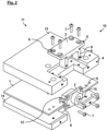
- Fig. 2
- shows an explosive perspective view of an electronic device with an RF connection system according to another embodiment of the present invention.
- The appended drawings are intended to provide further understanding of the embodiments of the invention. They illustrate embodiments and, in conjunction with the description, help to explain principles and concepts of the invention. Other embodiments and many of the advantages mentioned become apparent in view of the drawings. The elements in the drawings are not necessarily shown to scale.
- In the drawings, like, functionally equivalent and identically operating elements, features and components are provided with like reference signs in each case, unless stated otherwise.
-
Figures 1 and2 show explosive perspective views ofelectronic devices 11 being equipped withRF connection systems 10 according to embodiments of the present invention. - Radio frequency (RF) and/or coaxial connectors are a key component in RF and microwave applications where they are frequently used in test and measurement equipment to connect coaxial cables with the respective read-out or signal generating system components, e.g. in signal and spectrum analyzers and/or generators, test systems for antennas and other electromagnetic equipment, oscilloscopes etc. In most of these applications it is paramount to utilize connectors that allow accurate and repeatable measurements while being durable and highly performant at the same time.
- In light of the above, a suitable RF connection should not only be easy to assemble in order to safe costs and manufacturing time but should also provide a connection that is mechanically and electrically stable.
- On the other hand, outer portions of such measuring instruments (e.g. a cover, an enclosure, assembly portions, modules etc.) are often used as heat sinks for cooling the electronic circuits within the respective instrument. If an RF socket is connected directly to such a portion, high temperatures could occur at the RF socket that could adversely affect manual handling of these devices. Hence, also cooling issues should be taken into account when providing a suitable RF connector.
- With reference to the embodiments shown in
Figs. 1 and2 ,electronic devices 11, e.g. measuring instruments, are described in the following that offer improvements to the above mentioned issues. In both cases, the respectiveelectronic device 11 comprises aPCB 1 housed between anupper enclosure cover 13 and alower enclosure cover 14. All three of these components are recessed on one side (right-hand side inFig. 1 ) to accommodate theRF connection system 10. - In order to dissipate heat generated by the
PCB 1 during operation, theupper enclosure cover 13 is made from a material with suitable thermal conductivity, e.g. an aluminum alloy or similar, such that it functions as aheat sink 4 for thePCB 1. However, it is to be understood that in other embodiments also thelower enclosure cover 14 may additionally or alternatively be provided with these properties accordingly. - Specifically, the
RF connector 10 of the exemplary embodiments ofFigs. 1 and2 comprises anRF connector 2 mounted on top of thePCB 1 within a mounting portion of thePCB 1. TheRF connector 2 may be an integrated component that is soldered (or otherwise fastened) to thePCB 1 as one part. However, theRF connector 2 may also be assembled from several subcomponents on top of thePCB 1, e.g. by first soldering a basic RF socket to the PCB featuring a pre-installed coaxial terminal and subsequently attach an RF port to the RF socket that may adapt the coaxial terminal for larger connectors/cables, for example. - The
RF connector 10 provides a plug-inport 15 with a coaxial terminal inside (the latter is not visible in the figures). TheRF connector 10 in the shown embodiment features a small box-like or cuboid housing portion resting upon themounting portion 12 of thePCB 1 and a plate-shaped flange portion arranged on an outer side of theelectronic device 11 and having a cylindrical extension with a through-hole serving as plug-inport 15 for other RF connectors, via which coaxial cables and the like may contact thePCB 1. ThePCB 1 is configured with twoelongated holes 8 or slits running alongside the mountingportion 12 of thePCB 1, that is, adjacent to theRF connector 10 and parallel to a plug-in direction of the same. - The
electronic devices 11 ofFigs. 1 and2 each further comprise a mountingelement 3 mounted between theupper enclosure cover 13 serving asheat sink 4 and theRF connector 2 to thermally decouple theRF connector 2 from theheat sink 4. To this end, each mountingelement 3 is formed from a thermally insulating material, e.g. plastic. - The mounting
elements 3 of both embodiments are configured withalignment interfaces 5 for aligning theRF connector 2 with respect to theheat sink 4. More specifically, thealignment interfaces 5 compriseseveral fastening portions 6 configured as fastening holes for receivingfastening elements 7 in order to fasten theRF connector 2 to the mountingelement 3 and the mountingelement 3 to theheat sink 4, respectively. The alignment interfaces 5 thus serve as alignment and/or tolerance compensation means during installation of the assembly. - The purpose of the mounting
elements 3 is thus twofold. On the one hand, they are used to thermally decouple theRF connector 2 from theheat sink 4. On top of that, they are used as alignment means to compensate potential tolerances within the assembly. - As can be seen in the figures, the mounting
elements 3 are accommodated in a graded recess within theupper enclosure cover 13, which also features correspondingly formed fastening holes such that the mountingelements 3 may be fixed in the recess by means offastening elements 7. It is to be understood of course that the depicted configurations are mere examples. In a similar vein, the mountingelements 3 could also be mounted in/on thelower enclosure cover 14 or in other portions of a housing of theelectronic device 11. - As can be seen in
Figs. 1 and2 , the mountingelements 3 are provided with different shapes in both embodiments. In the embodiment ofFig. 1 , the mountingelement 3 has an elongated rectangular bar-like shape where thefastening portions 6 are arranged at both distal ends (two on top for fixing the mountingelement 3 to theupper enclosure cover 13 and two on a lateral side for attaching the RF connector 2). - In the embodiment of
Fig. 2 , the mountingelement 3 has a plate-shaped upper portion resting on the graded recess in theupper enclosure cover 13 and fastened there by means of four fastening holes at each corner. Twoteeth 9 protrude from a lower side of the plate-shaped portion, eachtooth 9 configured with two fastening holes for attachment of theRF connector 10. Theteeth 9 are adapted to engage theelongated holes 8 at each lateral side of the mountingportion 12. In this vein, mechanical stress may be deflected from the mountingportion 12. For example, mechanical loads induced in theRF connector 2 from the outside may be absorbed and/or compensated by theteeth 9 of the mountingelement 3 such that mechanical stress can be kept away from the mountingportion 12. - The mounting
element 3 in the embodiment ofFig. 2 thus further helps to compensate mechanical stress during assembly and operation to make sure that the soldered connection between thePCB 1 and theRF connector 2 does not suffer unnecessarily under mechanical loads. - Although specific embodiments have been illustrated and described herein, it will be appreciated by those of ordinary skill in the art that a variety of alternate and/or equivalent implementations exist. It should be appreciated that the exemplary embodiment or exemplary embodiments are only examples, and are not intended to limit the scope, applicability, or configuration in any way. Rather, the foregoing summary and detailed description will provide those skilled in the art with a convenient road map for implementing at least one exemplary embodiment, it being understood that various changes may be made in the function and arrangement of elements described in an exemplary embodiment without departing from the scope as set forth in the appended claims and their legal equivalents. Generally, this application is intended to cover any adaptations or variations of the specific embodiments discussed herein.
- In the foregoing detailed description, various features are grouped together in one or more examples or examples for the purpose of streamlining the disclosure. It is understood that the above description is intended to be illustrative, and not restrictive. It is intended to cover all alternatives, modifications and equivalents as may be included within the scope of the invention. Many other examples will be apparent to one skilled in the art upon reviewing the above specification.
- Specific nomenclature used in the foregoing specification is used to provide a thorough understanding of the invention. However, it will be apparent to one skilled in the art in light of the specification provided herein that the specific details are not required in order to practice the invention. Thus, the foregoing descriptions of specific embodiments of the present invention are presented for purposes of illustration and description. They are not intended to be exhaustive or to limit the invention to the precise forms disclosed; obviously many modifications and variations are possible in view of the above teachings. The embodiments were chosen and described in order to best explain the principles of the invention and its practical applications, to thereby enable others skilled in the art to best utilize the invention and various embodiments with various modifications as are suited to the particular use contemplated. Throughout the specification, the terms "including" and "in which" are used as the plain-English equivalents of the respective terms "comprising" and "wherein," respectively. Moreover, the terms "first," "second," and "third," etc., are used merely as labels, and are not intended to impose numerical requirements on or to establish a certain ranking of importance of their objects.
-
- 1
- printed circuit board (PCB)
- 2
- RF connector
- 3
- mounting element
- 4
- heat sink
- 5
- alignment interface
- 6
- fastening portion
- 7
- fastening element
- 8
- elongated hole
- 9
- tooth
- 10
- RF connection system
- 11
- electronic device
- 12
- mounting portion
- 13
- upper enclosure cover
- 14
- lower enclosure cover
- 15
- plug-in port
Claims (8)
- RF connection system (10) for contacting a printed circuit board, PCB, (1), the RF connection system (10) comprising:an RF connector (2) configured to be mounted to the PCB (1); anda mounting element (3) configured to be mounted between a heat sink (4) of the PCB (1) and the RF connector (2) to thermally decouple the RF connector (2) from the heat sink (4), wherein the mounting element (3) comprises at least one alignment interface (5) for aligning the RF connector (2) with respect to the heat sink (4).
- RF connection system according to claim 1, wherein the mounting element (3) comprises a thermally insulating material.
- RF connection system according to claim 1 or 2, wherein the at least one alignment interface (5) comprises several fastening portions (6) for fastening the RF connector (2) to the mounting element (3) and the mounting element (3) to the heat sink (4), respectively.
- RF connection system according to claim 3, wherein each fastening portion (6) is configured as a fastening hole for receiving a fastening element (7).
- Electronic device (11), comprising:a PCB (1);a heat sink (4) connected to the PCB (1) and configured to dissipate heat generated by the PCB (1); andan RF connection system (10) according to one of the claims 1 to 4 mounted between the heat sink (4) and the PCB (1).
- Electronic device according to claim 5, wherein the PCB (1) is configured with at least one groove or elongated hole (8) running alongside a mounting portion (12) of the PCB (1), on which the RF connector (2) is mounted to the PCB (1).
- Electronic device according to claim 5 or 6, wherein the mounting element (3) is configured with at least one tooth (9) configured to engage the at least one groove or elongated hole (8) to deflect mechanical stress from the mounting portion (12).
- Electronic device according to one of the claims 5 to 7, wherein the heat sink (4) is part of a thermally conductive enclosure (13, 14) of the PCB (1).
Priority Applications (1)
| Application Number | Priority Date | Filing Date | Title |
|---|---|---|---|
| EP21209001.3A EP4185080B1 (en) | 2021-11-18 | 2021-11-18 | Rf connection system, electronic device |
Applications Claiming Priority (1)
| Application Number | Priority Date | Filing Date | Title |
|---|---|---|---|
| EP21209001.3A EP4185080B1 (en) | 2021-11-18 | 2021-11-18 | Rf connection system, electronic device |
Publications (2)
| Publication Number | Publication Date |
|---|---|
| EP4185080A1 true EP4185080A1 (en) | 2023-05-24 |
| EP4185080B1 EP4185080B1 (en) | 2025-01-01 |
Family
ID=78819277
Family Applications (1)
| Application Number | Title | Priority Date | Filing Date |
|---|---|---|---|
| EP21209001.3A Active EP4185080B1 (en) | 2021-11-18 | 2021-11-18 | Rf connection system, electronic device |
Country Status (1)
| Country | Link |
|---|---|
| EP (1) | EP4185080B1 (en) |
Citations (3)
| Publication number | Priority date | Publication date | Assignee | Title |
|---|---|---|---|---|
| US20020171994A1 (en) * | 2001-05-15 | 2002-11-21 | Applied Materials, Inc. | Apparatus for regulating temperature of a process kit in a semiconductor wafer-processing chamber |
| US7018216B1 (en) | 2005-06-06 | 2006-03-28 | Harris Corporation | Coaxial connector for circuit boards |
| DE102008022100A1 (en) | 2008-04-15 | 2009-10-22 | Rohde & Schwarz Gmbh & Co. Kg | Coaxial connector with thermal decoupling |
-
2021
- 2021-11-18 EP EP21209001.3A patent/EP4185080B1/en active Active
Patent Citations (3)
| Publication number | Priority date | Publication date | Assignee | Title |
|---|---|---|---|---|
| US20020171994A1 (en) * | 2001-05-15 | 2002-11-21 | Applied Materials, Inc. | Apparatus for regulating temperature of a process kit in a semiconductor wafer-processing chamber |
| US7018216B1 (en) | 2005-06-06 | 2006-03-28 | Harris Corporation | Coaxial connector for circuit boards |
| DE102008022100A1 (en) | 2008-04-15 | 2009-10-22 | Rohde & Schwarz Gmbh & Co. Kg | Coaxial connector with thermal decoupling |
Also Published As
| Publication number | Publication date |
|---|---|
| EP4185080B1 (en) | 2025-01-01 |
Similar Documents
| Publication | Publication Date | Title |
|---|---|---|
| US7416332B2 (en) | Flexible circuit temperature sensor assembly for flanged mounted electronic devices | |
| US8238108B2 (en) | Power semiconductor module system | |
| EP1238574B1 (en) | Integrated convection and conduction heat sink for multiple mounting positions | |
| US7018216B1 (en) | Coaxial connector for circuit boards | |
| US20070249187A1 (en) | Power supply device | |
| US8116099B2 (en) | Circuit board device, electronic device provided with the same, and GND connecting method | |
| CN110417280B (en) | Electronic module of inverter and installation method thereof | |
| JP4697163B2 (en) | Electronic equipment | |
| US8157571B2 (en) | High-frequency module having a coaxial connector with its center conductor contacting a print wiring at only one point | |
| KR100959427B1 (en) | Electronic circuit apparatus for compressor | |
| WO2007125974A1 (en) | Conductive contact holder | |
| EP3327767B1 (en) | Mount structure, method of manufacturing mount structure, and wireless device | |
| CN106404268B (en) | Pressure sensor and method for producing such a pressure sensor | |
| JP2009524179A (en) | RF connector installation means | |
| US11081828B2 (en) | Power module housing | |
| CN106404235B (en) | Pressure sensor and method for producing such a pressure sensor | |
| US7795543B2 (en) | Electrical device | |
| JP2020145420A (en) | Mounting equipment for semiconductor packages | |
| WO2010050132A1 (en) | Testing device and circuit module | |
| EP4185080B1 (en) | Rf connection system, electronic device | |
| US7593235B2 (en) | Thermal conduit | |
| US6869293B2 (en) | Electronic device having integrated connector | |
| CN111416245A (en) | Plug-in connection unit with shield bracket | |
| EP4184728B1 (en) | Rf connector for contacting a printed circuit board | |
| CN222838698U (en) | Capacitor module and electrical equipment |
Legal Events
| Date | Code | Title | Description |
|---|---|---|---|
| PUAI | Public reference made under article 153(3) epc to a published international application that has entered the european phase |
Free format text: ORIGINAL CODE: 0009012 |
|
| STAA | Information on the status of an ep patent application or granted ep patent |
Free format text: STATUS: THE APPLICATION HAS BEEN PUBLISHED |
|
| AK | Designated contracting states |
Kind code of ref document: A1 Designated state(s): AL AT BE BG CH CY CZ DE DK EE ES FI FR GB GR HR HU IE IS IT LI LT LU LV MC MK MT NL NO PL PT RO RS SE SI SK SM TR |
|
| P01 | Opt-out of the competence of the unified patent court (upc) registered |
Effective date: 20230525 |
|
| STAA | Information on the status of an ep patent application or granted ep patent |
Free format text: STATUS: REQUEST FOR EXAMINATION WAS MADE |
|
| 17P | Request for examination filed |
Effective date: 20231020 |
|
| RBV | Designated contracting states (corrected) |
Designated state(s): AL AT BE BG CH CY CZ DE DK EE ES FI FR GB GR HR HU IE IS IT LI LT LU LV MC MK MT NL NO PL PT RO RS SE SI SK SM TR |
|
| GRAP | Despatch of communication of intention to grant a patent |
Free format text: ORIGINAL CODE: EPIDOSNIGR1 |
|
| STAA | Information on the status of an ep patent application or granted ep patent |
Free format text: STATUS: GRANT OF PATENT IS INTENDED |
|
| INTG | Intention to grant announced |
Effective date: 20240711 |
|
| GRAS | Grant fee paid |
Free format text: ORIGINAL CODE: EPIDOSNIGR3 |
|
| RBV | Designated contracting states (corrected) |
Designated state(s): AL AT BE BG CY CZ DE DK EE ES FI FR GB GR HR HU IS IT LT LU LV MC MK MT NL NO PL PT RO RS SE SI SK SM TR |
|
| GRAA | (expected) grant |
Free format text: ORIGINAL CODE: 0009210 |
|
| STAA | Information on the status of an ep patent application or granted ep patent |
Free format text: STATUS: THE PATENT HAS BEEN GRANTED |
|
| AK | Designated contracting states |
Kind code of ref document: B1 Designated state(s): AL AT BE BG CY CZ DE DK EE ES FI FR GB GR HR HU IS IT LT LU LV MC MK MT NL NO PL PT RO RS SE SI SK SM TR |
|
| REG | Reference to a national code |
Ref country code: GB Ref legal event code: FG4D |
|
| REG | Reference to a national code |
Ref country code: DE Ref legal event code: R096 Ref document number: 602021024186 Country of ref document: DE |
|
| REG | Reference to a national code |
Ref country code: LT Ref legal event code: MG9D |
|
| REG | Reference to a national code |
Ref country code: NL Ref legal event code: MP Effective date: 20250101 |
|
| REG | Reference to a national code |
Ref country code: AT Ref legal event code: MK05 Ref document number: 1757664 Country of ref document: AT Kind code of ref document: T Effective date: 20250101 |
|
| PG25 | Lapsed in a contracting state [announced via postgrant information from national office to epo] |
Ref country code: NL Free format text: LAPSE BECAUSE OF FAILURE TO SUBMIT A TRANSLATION OF THE DESCRIPTION OR TO PAY THE FEE WITHIN THE PRESCRIBED TIME-LIMIT Effective date: 20250101 |
|
| PG25 | Lapsed in a contracting state [announced via postgrant information from national office to epo] |
Ref country code: FI Free format text: LAPSE BECAUSE OF FAILURE TO SUBMIT A TRANSLATION OF THE DESCRIPTION OR TO PAY THE FEE WITHIN THE PRESCRIBED TIME-LIMIT Effective date: 20250101 |
|
| PG25 | Lapsed in a contracting state [announced via postgrant information from national office to epo] |
Ref country code: PL Free format text: LAPSE BECAUSE OF FAILURE TO SUBMIT A TRANSLATION OF THE DESCRIPTION OR TO PAY THE FEE WITHIN THE PRESCRIBED TIME-LIMIT Effective date: 20250101 |
|
| PG25 | Lapsed in a contracting state [announced via postgrant information from national office to epo] |
Ref country code: ES Free format text: LAPSE BECAUSE OF FAILURE TO SUBMIT A TRANSLATION OF THE DESCRIPTION OR TO PAY THE FEE WITHIN THE PRESCRIBED TIME-LIMIT Effective date: 20250101 |
|
| PG25 | Lapsed in a contracting state [announced via postgrant information from national office to epo] |
Ref country code: NO Free format text: LAPSE BECAUSE OF FAILURE TO SUBMIT A TRANSLATION OF THE DESCRIPTION OR TO PAY THE FEE WITHIN THE PRESCRIBED TIME-LIMIT Effective date: 20250401 Ref country code: IS Free format text: LAPSE BECAUSE OF FAILURE TO SUBMIT A TRANSLATION OF THE DESCRIPTION OR TO PAY THE FEE WITHIN THE PRESCRIBED TIME-LIMIT Effective date: 20250501 |
|
| PG25 | Lapsed in a contracting state [announced via postgrant information from national office to epo] |
Ref country code: HR Free format text: LAPSE BECAUSE OF FAILURE TO SUBMIT A TRANSLATION OF THE DESCRIPTION OR TO PAY THE FEE WITHIN THE PRESCRIBED TIME-LIMIT Effective date: 20250101 |
|
| PG25 | Lapsed in a contracting state [announced via postgrant information from national office to epo] |
Ref country code: PT Free format text: LAPSE BECAUSE OF FAILURE TO SUBMIT A TRANSLATION OF THE DESCRIPTION OR TO PAY THE FEE WITHIN THE PRESCRIBED TIME-LIMIT Effective date: 20250502 Ref country code: LV Free format text: LAPSE BECAUSE OF FAILURE TO SUBMIT A TRANSLATION OF THE DESCRIPTION OR TO PAY THE FEE WITHIN THE PRESCRIBED TIME-LIMIT Effective date: 20250101 |
|
| PG25 | Lapsed in a contracting state [announced via postgrant information from national office to epo] |
Ref country code: BG Free format text: LAPSE BECAUSE OF FAILURE TO SUBMIT A TRANSLATION OF THE DESCRIPTION OR TO PAY THE FEE WITHIN THE PRESCRIBED TIME-LIMIT Effective date: 20250101 Ref country code: GR Free format text: LAPSE BECAUSE OF FAILURE TO SUBMIT A TRANSLATION OF THE DESCRIPTION OR TO PAY THE FEE WITHIN THE PRESCRIBED TIME-LIMIT Effective date: 20250402 |
|
| PG25 | Lapsed in a contracting state [announced via postgrant information from national office to epo] |
Ref country code: AT Free format text: LAPSE BECAUSE OF FAILURE TO SUBMIT A TRANSLATION OF THE DESCRIPTION OR TO PAY THE FEE WITHIN THE PRESCRIBED TIME-LIMIT Effective date: 20250101 |
|
| PG25 | Lapsed in a contracting state [announced via postgrant information from national office to epo] |
Ref country code: CZ Free format text: LAPSE BECAUSE OF FAILURE TO SUBMIT A TRANSLATION OF THE DESCRIPTION OR TO PAY THE FEE WITHIN THE PRESCRIBED TIME-LIMIT Effective date: 20250101 |
|
| PG25 | Lapsed in a contracting state [announced via postgrant information from national office to epo] |
Ref country code: SE Free format text: LAPSE BECAUSE OF FAILURE TO SUBMIT A TRANSLATION OF THE DESCRIPTION OR TO PAY THE FEE WITHIN THE PRESCRIBED TIME-LIMIT Effective date: 20250101 |
|
| REG | Reference to a national code |
Ref country code: DE Ref legal event code: R097 Ref document number: 602021024186 Country of ref document: DE |
|
| PG25 | Lapsed in a contracting state [announced via postgrant information from national office to epo] |
Ref country code: SM Free format text: LAPSE BECAUSE OF FAILURE TO SUBMIT A TRANSLATION OF THE DESCRIPTION OR TO PAY THE FEE WITHIN THE PRESCRIBED TIME-LIMIT Effective date: 20250101 |
|
| PG25 | Lapsed in a contracting state [announced via postgrant information from national office to epo] |
Ref country code: DK Free format text: LAPSE BECAUSE OF FAILURE TO SUBMIT A TRANSLATION OF THE DESCRIPTION OR TO PAY THE FEE WITHIN THE PRESCRIBED TIME-LIMIT Effective date: 20250101 |
|
| PG25 | Lapsed in a contracting state [announced via postgrant information from national office to epo] |
Ref country code: IT Free format text: LAPSE BECAUSE OF FAILURE TO SUBMIT A TRANSLATION OF THE DESCRIPTION OR TO PAY THE FEE WITHIN THE PRESCRIBED TIME-LIMIT Effective date: 20250101 |
|
| PG25 | Lapsed in a contracting state [announced via postgrant information from national office to epo] |
Ref country code: EE Free format text: LAPSE BECAUSE OF FAILURE TO SUBMIT A TRANSLATION OF THE DESCRIPTION OR TO PAY THE FEE WITHIN THE PRESCRIBED TIME-LIMIT Effective date: 20250101 |
|
| PG25 | Lapsed in a contracting state [announced via postgrant information from national office to epo] |
Ref country code: RO Free format text: LAPSE BECAUSE OF FAILURE TO SUBMIT A TRANSLATION OF THE DESCRIPTION OR TO PAY THE FEE WITHIN THE PRESCRIBED TIME-LIMIT Effective date: 20250101 |
|
| PG25 | Lapsed in a contracting state [announced via postgrant information from national office to epo] |
Ref country code: SK Free format text: LAPSE BECAUSE OF FAILURE TO SUBMIT A TRANSLATION OF THE DESCRIPTION OR TO PAY THE FEE WITHIN THE PRESCRIBED TIME-LIMIT Effective date: 20250101 |
|
| PLBE | No opposition filed within time limit |
Free format text: ORIGINAL CODE: 0009261 |
|
| STAA | Information on the status of an ep patent application or granted ep patent |
Free format text: STATUS: NO OPPOSITION FILED WITHIN TIME LIMIT |
|
| 26N | No opposition filed |
Effective date: 20251002 |
|
| PGFP | Annual fee paid to national office [announced via postgrant information from national office to epo] |
Ref country code: DE Payment date: 20251118 Year of fee payment: 5 |
|
| PGFP | Annual fee paid to national office [announced via postgrant information from national office to epo] |
Ref country code: GB Payment date: 20251120 Year of fee payment: 5 |
|
| PGFP | Annual fee paid to national office [announced via postgrant information from national office to epo] |
Ref country code: FR Payment date: 20251125 Year of fee payment: 5 |
|
| PG25 | Lapsed in a contracting state [announced via postgrant information from national office to epo] |
Ref country code: LT Free format text: LAPSE BECAUSE OF FAILURE TO SUBMIT A TRANSLATION OF THE DESCRIPTION OR TO PAY THE FEE WITHIN THE PRESCRIBED TIME-LIMIT Effective date: 20250101 |
|
| PG25 | Lapsed in a contracting state [announced via postgrant information from national office to epo] |
Ref country code: MC Free format text: LAPSE BECAUSE OF FAILURE TO SUBMIT A TRANSLATION OF THE DESCRIPTION OR TO PAY THE FEE WITHIN THE PRESCRIBED TIME-LIMIT Effective date: 20250101 |
|
| PG25 | Lapsed in a contracting state [announced via postgrant information from national office to epo] |
Ref country code: RS Free format text: LAPSE BECAUSE OF FAILURE TO SUBMIT A TRANSLATION OF THE DESCRIPTION OR TO PAY THE FEE WITHIN THE PRESCRIBED TIME-LIMIT Effective date: 20250101 |
|
| PG25 | Lapsed in a contracting state [announced via postgrant information from national office to epo] |
Ref country code: LU Free format text: LAPSE BECAUSE OF NON-PAYMENT OF DUE FEES Effective date: 20251118 |