EP4184570A2 - Power electronic module with reduced mutual inductance between power and control loops - Google Patents
Power electronic module with reduced mutual inductance between power and control loops Download PDFInfo
- Publication number
- EP4184570A2 EP4184570A2 EP22193410.2A EP22193410A EP4184570A2 EP 4184570 A2 EP4184570 A2 EP 4184570A2 EP 22193410 A EP22193410 A EP 22193410A EP 4184570 A2 EP4184570 A2 EP 4184570A2
- Authority
- EP
- European Patent Office
- Prior art keywords
- power
- control
- switching element
- power part
- terminal
- Prior art date
- Legal status (The legal status is an assumption and is not a legal conclusion. Google has not performed a legal analysis and makes no representation as to the accuracy of the status listed.)
- Pending
Links
Images





Classifications
-
- H—ELECTRICITY
- H10—SEMICONDUCTOR DEVICES; ELECTRIC SOLID-STATE DEVICES NOT OTHERWISE PROVIDED FOR
- H10W—GENERIC PACKAGES, INTERCONNECTIONS, CONNECTORS OR OTHER CONSTRUCTIONAL DETAILS OF DEVICES COVERED BY CLASS H10
- H10W90/00—Package configurations
- H10W90/811—Multiple chips on leadframes
-
- H—ELECTRICITY
- H02—GENERATION; CONVERSION OR DISTRIBUTION OF ELECTRIC POWER
- H02M—APPARATUS FOR CONVERSION BETWEEN AC AND AC, BETWEEN AC AND DC, OR BETWEEN DC AND DC, AND FOR USE WITH MAINS OR SIMILAR POWER SUPPLY SYSTEMS; CONVERSION OF DC OR AC INPUT POWER INTO SURGE OUTPUT POWER; CONTROL OR REGULATION THEREOF
- H02M3/00—Conversion of DC power input into DC power output
- H02M3/02—Conversion of DC power input into DC power output without intermediate conversion into AC
- H02M3/04—Conversion of DC power input into DC power output without intermediate conversion into AC by static converters
- H02M3/10—Conversion of DC power input into DC power output without intermediate conversion into AC by static converters using discharge tubes with control electrode or semiconductor devices with control electrode
- H02M3/145—Conversion of DC power input into DC power output without intermediate conversion into AC by static converters using discharge tubes with control electrode or semiconductor devices with control electrode using devices of a triode or transistor type requiring continuous application of a control signal
- H02M3/155—Conversion of DC power input into DC power output without intermediate conversion into AC by static converters using discharge tubes with control electrode or semiconductor devices with control electrode using devices of a triode or transistor type requiring continuous application of a control signal using semiconductor devices only
- H02M3/156—Conversion of DC power input into DC power output without intermediate conversion into AC by static converters using discharge tubes with control electrode or semiconductor devices with control electrode using devices of a triode or transistor type requiring continuous application of a control signal using semiconductor devices only with automatic control of output voltage or current, e.g. switching regulators
- H02M3/158—Conversion of DC power input into DC power output without intermediate conversion into AC by static converters using discharge tubes with control electrode or semiconductor devices with control electrode using devices of a triode or transistor type requiring continuous application of a control signal using semiconductor devices only with automatic control of output voltage or current, e.g. switching regulators including plural semiconductor devices as final control devices for a single load
- H02M3/1584—Conversion of DC power input into DC power output without intermediate conversion into AC by static converters using discharge tubes with control electrode or semiconductor devices with control electrode using devices of a triode or transistor type requiring continuous application of a control signal using semiconductor devices only with automatic control of output voltage or current, e.g. switching regulators including plural semiconductor devices as final control devices for a single load with a plurality of power processing stages connected in parallel
-
- H—ELECTRICITY
- H02—GENERATION; CONVERSION OR DISTRIBUTION OF ELECTRIC POWER
- H02M—APPARATUS FOR CONVERSION BETWEEN AC AND AC, BETWEEN AC AND DC, OR BETWEEN DC AND DC, AND FOR USE WITH MAINS OR SIMILAR POWER SUPPLY SYSTEMS; CONVERSION OF DC OR AC INPUT POWER INTO SURGE OUTPUT POWER; CONTROL OR REGULATION THEREOF
- H02M1/00—Details of apparatus for conversion
- H02M1/0048—Circuits or arrangements for reducing losses
-
- H—ELECTRICITY
- H02—GENERATION; CONVERSION OR DISTRIBUTION OF ELECTRIC POWER
- H02M—APPARATUS FOR CONVERSION BETWEEN AC AND AC, BETWEEN AC AND DC, OR BETWEEN DC AND DC, AND FOR USE WITH MAINS OR SIMILAR POWER SUPPLY SYSTEMS; CONVERSION OF DC OR AC INPUT POWER INTO SURGE OUTPUT POWER; CONTROL OR REGULATION THEREOF
- H02M1/00—Details of apparatus for conversion
- H02M1/0064—Magnetic structures combining different functions, e.g. storage, filtering or transformation
-
- H—ELECTRICITY
- H02—GENERATION; CONVERSION OR DISTRIBUTION OF ELECTRIC POWER
- H02M—APPARATUS FOR CONVERSION BETWEEN AC AND AC, BETWEEN AC AND DC, OR BETWEEN DC AND DC, AND FOR USE WITH MAINS OR SIMILAR POWER SUPPLY SYSTEMS; CONVERSION OF DC OR AC INPUT POWER INTO SURGE OUTPUT POWER; CONTROL OR REGULATION THEREOF
- H02M1/00—Details of apparatus for conversion
- H02M1/44—Circuits or arrangements for compensating for electromagnetic interference in converters or inverters
-
- H—ELECTRICITY
- H02—GENERATION; CONVERSION OR DISTRIBUTION OF ELECTRIC POWER
- H02M—APPARATUS FOR CONVERSION BETWEEN AC AND AC, BETWEEN AC AND DC, OR BETWEEN DC AND DC, AND FOR USE WITH MAINS OR SIMILAR POWER SUPPLY SYSTEMS; CONVERSION OF DC OR AC INPUT POWER INTO SURGE OUTPUT POWER; CONTROL OR REGULATION THEREOF
- H02M3/00—Conversion of DC power input into DC power output
- H02M3/003—Constructional details, e.g. physical layout, assembly, wiring or busbar connections
-
- H—ELECTRICITY
- H10—SEMICONDUCTOR DEVICES; ELECTRIC SOLID-STATE DEVICES NOT OTHERWISE PROVIDED FOR
- H10W—GENERIC PACKAGES, INTERCONNECTIONS, CONNECTORS OR OTHER CONSTRUCTIONAL DETAILS OF DEVICES COVERED BY CLASS H10
- H10W44/00—Electrical arrangements for controlling or matching impedance
- H10W44/501—Inductive arrangements
-
- H—ELECTRICITY
- H10—SEMICONDUCTOR DEVICES; ELECTRIC SOLID-STATE DEVICES NOT OTHERWISE PROVIDED FOR
- H10W—GENERIC PACKAGES, INTERCONNECTIONS, CONNECTORS OR OTHER CONSTRUCTIONAL DETAILS OF DEVICES COVERED BY CLASS H10
- H10W70/00—Package substrates; Interposers; Redistribution layers [RDL]
- H10W70/40—Leadframes
- H10W70/481—Leadframes for devices being provided for in groups H10D8/00 - H10D48/00
-
- H—ELECTRICITY
- H10—SEMICONDUCTOR DEVICES; ELECTRIC SOLID-STATE DEVICES NOT OTHERWISE PROVIDED FOR
- H10W—GENERIC PACKAGES, INTERCONNECTIONS, CONNECTORS OR OTHER CONSTRUCTIONAL DETAILS OF DEVICES COVERED BY CLASS H10
- H10W90/00—Package configurations
-
- H—ELECTRICITY
- H10—SEMICONDUCTOR DEVICES; ELECTRIC SOLID-STATE DEVICES NOT OTHERWISE PROVIDED FOR
- H10W—GENERIC PACKAGES, INTERCONNECTIONS, CONNECTORS OR OTHER CONSTRUCTIONAL DETAILS OF DEVICES COVERED BY CLASS H10
- H10W72/00—Interconnections or connectors in packages
- H10W72/30—Die-attach connectors
-
- H—ELECTRICITY
- H10—SEMICONDUCTOR DEVICES; ELECTRIC SOLID-STATE DEVICES NOT OTHERWISE PROVIDED FOR
- H10W—GENERIC PACKAGES, INTERCONNECTIONS, CONNECTORS OR OTHER CONSTRUCTIONAL DETAILS OF DEVICES COVERED BY CLASS H10
- H10W72/00—Interconnections or connectors in packages
- H10W72/50—Bond wires
- H10W72/541—Dispositions of bond wires
- H10W72/5449—Dispositions of bond wires not being orthogonal to a side surface of the chip, e.g. fan-out arrangements
-
- H—ELECTRICITY
- H10—SEMICONDUCTOR DEVICES; ELECTRIC SOLID-STATE DEVICES NOT OTHERWISE PROVIDED FOR
- H10W—GENERIC PACKAGES, INTERCONNECTIONS, CONNECTORS OR OTHER CONSTRUCTIONAL DETAILS OF DEVICES COVERED BY CLASS H10
- H10W72/00—Interconnections or connectors in packages
- H10W72/50—Bond wires
- H10W72/541—Dispositions of bond wires
- H10W72/547—Dispositions of multiple bond wires
- H10W72/5473—Dispositions of multiple bond wires multiple bond wires connected to a common bond pad
-
- H—ELECTRICITY
- H10—SEMICONDUCTOR DEVICES; ELECTRIC SOLID-STATE DEVICES NOT OTHERWISE PROVIDED FOR
- H10W—GENERIC PACKAGES, INTERCONNECTIONS, CONNECTORS OR OTHER CONSTRUCTIONAL DETAILS OF DEVICES COVERED BY CLASS H10
- H10W72/00—Interconnections or connectors in packages
- H10W72/50—Bond wires
- H10W72/541—Dispositions of bond wires
- H10W72/547—Dispositions of multiple bond wires
- H10W72/5475—Dispositions of multiple bond wires multiple bond wires connected to common bond pads at both ends of the wires
-
- H—ELECTRICITY
- H10—SEMICONDUCTOR DEVICES; ELECTRIC SOLID-STATE DEVICES NOT OTHERWISE PROVIDED FOR
- H10W—GENERIC PACKAGES, INTERCONNECTIONS, CONNECTORS OR OTHER CONSTRUCTIONAL DETAILS OF DEVICES COVERED BY CLASS H10
- H10W72/00—Interconnections or connectors in packages
- H10W72/851—Dispositions of multiple connectors or interconnections
- H10W72/874—On different surfaces
- H10W72/884—Die-attach connectors and bond wires
-
- H—ELECTRICITY
- H10—SEMICONDUCTOR DEVICES; ELECTRIC SOLID-STATE DEVICES NOT OTHERWISE PROVIDED FOR
- H10W—GENERIC PACKAGES, INTERCONNECTIONS, CONNECTORS OR OTHER CONSTRUCTIONAL DETAILS OF DEVICES COVERED BY CLASS H10
- H10W72/00—Interconnections or connectors in packages
- H10W72/90—Bond pads, in general
- H10W72/921—Structures or relative sizes of bond pads
- H10W72/926—Multiple bond pads having different sizes
-
- H—ELECTRICITY
- H10—SEMICONDUCTOR DEVICES; ELECTRIC SOLID-STATE DEVICES NOT OTHERWISE PROVIDED FOR
- H10W—GENERIC PACKAGES, INTERCONNECTIONS, CONNECTORS OR OTHER CONSTRUCTIONAL DETAILS OF DEVICES COVERED BY CLASS H10
- H10W90/00—Package configurations
- H10W90/701—Package configurations characterised by the relative positions of pads or connectors relative to package parts
- H10W90/751—Package configurations characterised by the relative positions of pads or connectors relative to package parts of bond wires
- H10W90/753—Package configurations characterised by the relative positions of pads or connectors relative to package parts of bond wires between laterally-adjacent chips
-
- H—ELECTRICITY
- H10—SEMICONDUCTOR DEVICES; ELECTRIC SOLID-STATE DEVICES NOT OTHERWISE PROVIDED FOR
- H10W—GENERIC PACKAGES, INTERCONNECTIONS, CONNECTORS OR OTHER CONSTRUCTIONAL DETAILS OF DEVICES COVERED BY CLASS H10
- H10W90/00—Package configurations
- H10W90/701—Package configurations characterised by the relative positions of pads or connectors relative to package parts
- H10W90/751—Package configurations characterised by the relative positions of pads or connectors relative to package parts of bond wires
- H10W90/756—Package configurations characterised by the relative positions of pads or connectors relative to package parts of bond wires between a chip and a stacked lead frame, conducting package substrate or heat sink
-
- Y—GENERAL TAGGING OF NEW TECHNOLOGICAL DEVELOPMENTS; GENERAL TAGGING OF CROSS-SECTIONAL TECHNOLOGIES SPANNING OVER SEVERAL SECTIONS OF THE IPC; TECHNICAL SUBJECTS COVERED BY FORMER USPC CROSS-REFERENCE ART COLLECTIONS [XRACs] AND DIGESTS
- Y02—TECHNOLOGIES OR APPLICATIONS FOR MITIGATION OR ADAPTATION AGAINST CLIMATE CHANGE
- Y02B—CLIMATE CHANGE MITIGATION TECHNOLOGIES RELATED TO BUILDINGS, e.g. HOUSING, HOUSE APPLIANCES OR RELATED END-USER APPLICATIONS
- Y02B70/00—Technologies for an efficient end-user side electric power management and consumption
- Y02B70/10—Technologies improving the efficiency by using switched-mode power supplies [SMPS], i.e. efficient power electronics conversion e.g. power factor correction or reduction of losses in power supplies or efficient standby modes
Definitions
- the present disclosure relates to a switching module, and more particularly to a switching module for reducing the mutual inductance between a power loop and a control loop.
- a switching module of a power electronic system operates at a high frequency to achieve high power density.
- the high operating frequency may increase the switching loss, and thus reduce the efficiency of the switching module. Consequently, when the switching module operates at the high frequency, it is necessary to increase the switching speed of the switching module in order to reduce the switching loss.
- EMI electromagnetic interference
- the power loop is relatively close to the control loop.
- the induced magnetic field also changes around the power loop.
- the induced magnetic field passes through the control loop, a corresponding induced voltage is generated in the control loop. Consequently, the electromagnetic interference of the mutual inductance between the power loop and the control loop is formed, which affects the switching operation of the switching module.
- a plurality of power loops are located beside each other, and a plurality of control loops are located beside each other.
- no control loop is arranged between every two adjacent power loops, and no power loop is arranged between every two adjacent control loops. Consequently, the induced magnetic fields generated by the power loops pass through the control loops in the same direction.
- the electromagnetic interference of the mutual inductance between the power loops and the control loops is largely increased. If the electromagnetic interference of the mutual inductance is too large, the interference voltage at a control terminal of the switching module may exceed the safe range. Under this circumstance, the reliability of the switching module is reduced, and the switching module is even unable to work normally.
- the present disclosure provides a switching module for reducing the mutual inductance between a power loop and a control loop.
- a switching module includes at least one substrate, at least one switching element, at least one control loop, a first power part and a second power part.
- the at least one switching element is disposed on the at least one substrate.
- the at least one control loop is connected with the corresponding switching element.
- the first power part is connected with the corresponding switching element.
- the second power part is connected with the corresponding switching element.
- a direction of a first current flowing through the first power part and a direction of a second current flowing through the second power part are identical.
- a projection of the first power part on a reference plane and a projection of the second power part on the reference plane are located at two opposite sides of a projection of the control loop on the reference plane.
- FIG. 1 is a schematic view illustrating the structure of a switching module according to a first embodiment of the present disclosure.
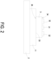
- FIG. 2 is a schematic side view illustrating a portion of the switching module as shown in FIG. 1 and taken along the section A-A'.
- FIG. 3 schematically illustrates the magnetic flux cancellation principle for the switching module as shown in FIG. 1 .
- the switching module 1 is disposed on a main circuit board (not shown) and electrically connected with the main circuit board.
- the switching module 1 includes a substrate 2, a switching element 3, a first control part 4, a second control part 5, a first power part 6 and a second power part 7.
- the switching element 3 is a vertical-type device.
- the switching element 3 is an insulated gate bipolar transistor (IGBT), a bipolar junction transistor (BJT), a metal-oxide-semiconductor field-effect transistor (MOSFET), a junction field effect transistor (JFET) or a gallium nitride high electron mobility transistor (GaN-HEMT).
- IGBT insulated gate bipolar transistor
- BJT bipolar junction transistor
- MOSFET metal-oxide-semiconductor field-effect transistor
- JFET junction field effect transistor
- GaN-HEMT gallium nitride high electron mobility transistor
- the switching element 3 is welded on the substrate 2 through a connecting material 11.
- the switching element 3 includes a first control terminal 31, a second control terminal, a first power terminal and a second power terminal 33.
- the first control terminal 31, the second control terminal and the first power terminal are disposed on a first surface 34 of the switching element 3. Since the second control terminal and the first power terminal are located at the same region of the switching element 3, the second control terminal and the first power terminal are also referred as a common conductive terminal 32.
- the second power terminal 33 is disposed on a second surface 35 of the switching element 3.
- the second power terminal 33 is connected with the substrate 2 through the connecting material 11.
- the switching element 3 is an insulated gate bipolar transistor (IGBT)
- the first control terminal 31 is served as a gate terminal of the switching element 3
- the common conductive terminal 32 i.e., the second control terminal and the first power terminal
- the second power terminal 33 is served as a collector of the switching element 3.
- the switching element 3 is a bipolar junction transistor (BJT)
- the first control terminal 31 is served as a base of the switching element 3
- the common conductive terminal 32 i.e., the second control terminal and the first power terminal
- the second power terminal 33 is served as a collector of the switching element 3.
- the switching element 3 is a metal-oxide-semiconductor field-effect transistor (MOSFET), a junction field effect transistor (JFET) or a gallium nitride high electron mobility transistor (GaN-HEMT)
- MOSFET metal-oxide-semiconductor field-effect transistor
- JFET junction field effect transistor
- GaN-HEMT gallium nitride high electron mobility transistor
- the first control part 4 is connected with the first control terminal 31 of the switching element 3.
- the first control part 4 includes a first control pin 41 and a first control conductor 42.
- the first control pin 41 is disposed on the main circuit board.
- the first control conductor 42 is connected between the first control pin 41 and the first control terminal 31 of the switching element 3.
- the second control part 5 is connected with the second control terminal (i.e., the common conductive terminal 32) of the switching element 3.
- the second control part 5 includes a second control pin 51 and a second control conductor 52.
- the second control pin 51 is disposed on the main circuit board.
- the second control conductor 52 is connected between the second control pin 51 and the second control terminal (i.e., the common conductive terminal 32) of the switching element 3.
- a control loop of the switching module 1 is defined by the second control terminal (i.e., the common conductive terminal 32), the second control conductor 52, the second control pin 51, the main circuit board, the first control pin 41, the first control conductor 42 and the first control terminal 31 collaboratively.
- the first power part 6 is connected with the first power terminal (i.e., the common conductive terminal 32) of the switching element 3.
- the first power part 6 includes a first power pin 61 and a first power conductor 62.
- the first power pin 61 is disposed on the main circuit board.
- the first power conductor 62 is connected between the first power pin 61 and the first power terminal (i.e., the common conductive terminal 32) of the switching element 3.
- a first current flows through the first power part 6.
- the second power part 7 is connected with the first power terminal (i.e., the common conductive terminal 32) of the switching element 3.
- the second power part 7 includes a second power pin 71 and a second power conductor 72.
- the second power pin 71 is disposed on the main circuit board.
- the second power conductor 72 is connected between the second power pin 71 and the first power terminal (i.e., the common conductive terminal 32) of the switching element 3.
- a second current flows through the second power part 7.
- the switching element 3 corresponding to the first power part 6 and the switching element 3 corresponding to the second power part 7 may be the identical or different switching elements 3.
- the first power part 6 and the second power part 7 may be connected with the same switching element 3 or respectively connected with two different switching elements 3.
- the direction of the first current flowing through the first power part 6 and the direction of the second current flowing through the second power part 7 are identical.
- the first current flows from the first power terminal (i.e., the common conductive terminal 32) to the first power pin 61 of the first power part 6 and the second current flows from the first power terminal (i.e., the common conductive terminal 32) to the second power pin 71 of the second power part 7, or the first current flows from the first power pin 61 of the first power part 6 to the first power terminal (i.e., the common conductive terminal 32) and the second current flows from the second power pin 71 of the second power part 7 to the first power terminal (i.e., the common conductive terminal 32). It is noted that numerous modifications and alterations may be made while retaining the teachings of the disclosure.
- the first power part 6 and the second power part 7 are connected with the second power terminal 33 of the corresponding switching element 3.
- the direction of the first current flowing through the first power part 6 and the direction of the second current flowing through the second power part 7 are identical.
- the first power part 6, the first control part 4, the second control part 5 and the second power part 7 are arranged sequentially.
- the projection of the first power part 6 on a reference plane and a projection of the second power part 7 on the same reference plane are located at two sides of a projection of the control loop of the switching module 1 (i.e., the control loop defined by the first control part 4 and the second control part 5) on the reference plane.
- the reference plane is coplanar with the substrate 2.
- the length of the first power part 6 is equal to the length of the second power part 7. Consequently, the current value of the first current flowing through the first power part 6 and the current value of the second current flowing through the second power part 7 are equal. Under this circumstance, the current value here refers to the amplitude of the corresponding current or the effective value of the corresponding current.
- FIG. 3 the projections of the first power part 6, the second power part 7 and the control loop on the reference plane are shown.
- the point A and the point B as shown in FIG. 3 denote two ends of the projection of the first control part 4 on the reference plane, respectively.
- the point C and the point D as shown in FIG. 3 denote two ends of the projection of the second control part 5 on the reference plane, respectively.
- the line P1 denotes the first current flowing through the first power part 6, and the line P2 denotes the second current flowing through the second power part 7.
- the point B and the point D are connected with each other through the main circuit board. Consequently, the rectangular region defined by the points A, B, C and D represents the projection of the control loop on the reference plane.
- the line O-O' represents the center line of the control loop on the reference plane. That is, the center line O-O' passes through the midpoint of a line segment connecting the point A and the point C, and the midpoint of a line segment connecting the point B and the point D.
- the projection of the first power part 6 on the reference plane and the projection of the second power part 7 on the reference plane are located at two sides of the projection of the control loop on the reference plane, respectively.
- the first current P1 flowing through the first power part 6 and the second current P2 flowing through the second power part 7 are symmetrical the two sides of the projection of the control loop on the reference plane.
- the distance between the projection of the first power part 6 on the reference plane and the center line O-O' is equal to the distance between the projection of the second power part 7 on the reference plane and the center line O-O'.
- the first current P1 flowing through the first power part 6 produces a total magnetic flux ⁇ 1 through the control loop.
- the second current P2 flowing through the second power part 7 produces a total magnetic flux ⁇ 2 through the control loop.
- the magnitude of the magnetic flux ⁇ 1 and the magnitude of the magnetic flux ⁇ 2 are equal, but the direction of the magnetic flux ⁇ 1 and the direction of the magnetic flux ⁇ 2 are opposite.
- the direction of the magnetic flux induced by the first current P1 through the control loop is perpendicular to the paper surface and inward
- the direction of the magnetic flux induced by the second current P2 through the control loop is perpendicular to the paper surface and outward.
- the magnetic flux ⁇ 1 and the magnetic flux ⁇ 2 are cancelled out. Consequently, the overall mutual inductance between the first power part 6, the second power part 7 and the control loop is largely reduced.
- the direction of the first current P1 flowing through the first power part 6 and the direction of the second current P2 flowing through the second power part 7 are identical.
- the projection of the first power part 6 on the reference plane and the projection of the second power part 7 on the same reference plane are located at two sides of the projection of the control loop of the switching module 1 on the reference plane.
- the mutual inductance between the power loop and the control loop in the switching module 1 of the present disclosure is reduced. Consequently, the safety performance of the switching module 1 is enhanced.
- the direction of the first current P1 and the direction of the second current P2 are identical. That is, the direction of the first current P1 and the direction of the second current P2 are in parallel with each other. It is noted that the direction of the first current P1 and the direction of the second current P2 are not restricted to be in parallel with each other. For example, in some embodiments, there is an angle between the direction of the first current P1 and the direction of the second current P2. The angle is smaller than 90 degrees. Particularly, after the first power part 6 and the second power part 7 are projected to a reference plane, the angle between first current P1 and the second current P2 is 0 degree or an acute angle.
- the reference plane is a plane coplanar with the substrate 2 or a plane that is perpendicular to the substrate 2 and passes through the center line O-O'.
- the direction of the first current P1 and the direction of the second current P2 are identical, but the first power part 6 and the second power part 7 are not completely symmetric with respect to the control loop or the magnitude of the first current P1 and the magnitude of the second current P2 are different. Since the direction of the magnetic flux ⁇ 1 corresponding to the first current P1 and the direction of the magnetic flux ⁇ 2 corresponding to the second current P2 are opposite, the magnetic flux ⁇ 1 and the magnetic flux ⁇ 2 are cancelled out. Consequently, the overall mutual inductance between the first power part 6, the second power part 7 and the control loop is largely reduced.
- the direction of the first current P1 flowing through the first power part 6 and the direction of the second current P2 flowing through the second power part 7 are in parallel with each other or tilted respective to each other. As long as the magnetic flux ⁇ 1 corresponding to the first current P1 and the magnetic flux ⁇ 2 corresponding to the second current P2 can be cancelled out and the mutual inductance is reduced, the installation positions of the first power part 6 and the second power part 7 are not restricted.
- FIG. 4 is a schematic view illustrating the structure of a switching module according to a second embodiment of the present disclosure.
- the switching module 1a of this embodiment further includes a fourth power part 9.
- the first power part 6 and the second power part 7 of the switching module 1a are connected with the second power terminal 33 of the corresponding switching element 3 through the substrate 2.
- the fourth power part 9 is connected with the common conductive terminal 32 of the corresponding switching element 3.
- the fourth power part 9 includes a fourth power pin 91 and the fourth power conductor 92.
- the fourth power pin 91 is disposed on the main circuit board.
- the fourth power conductor 92 is connected between the fourth power pin 91 and the common conductive terminal 32 of the corresponding switching element 3.
- the projection of the substrate 2 on the reference plane is a square with four sides.
- the projections of the first power part 6 and the second power part 7 are located at the same side with respect to the projection of the substrate 2.
- the projection of the fourth power part 9 and the projection of the first power part 6 (or the second power part 7) are located at different sides of the projection of the substrate 2.
- the projections of the first power part 6 and the second power part 7 are located at a first side of the projection of the substrate 2, and the projection of the fourth power part 9 is located at a second side of the projection of the substrate 2.
- the first side and the second side of the projection of the substrate 2 are opposite to each other.
- the first side and the second side of the projection of the substrate 2 are adjacent to each other.
- FIG. 5A is a schematic view illustrating the structure of a switching module according to a third embodiment of the present disclosure.
- FIG. 5B is a schematic circuit diagram of the switching module as shown in FIG. 5A .
- the structures and functions of the components of the switching module 1b which are identical to those of the first embodiment as shown in FIG. 1 are not redundantly described herein.
- the switching element 3 of the switching module 1 as shown in FIG. 1 has a vertical-type structure.
- the switching element 3 of the switching module 1b is a planar switching element. That is, the second power terminal 33, the first control terminal 31 and the common conductive terminal 32 are disposed on the first surface 34 of the switching element 3.
- the first power part 6 and the second power part 7 are connected with the common conductive terminal 32.
- the fourth power part 9 is connected with the second power terminal 33.
- FIG. 6 is a schematic view illustrating the structure of a switching module according to a fourth embodiment of the present disclosure.
- the switching module 1c includes two switching elements (i.e., a first switching element 3a and a second switching element 3b), two first control parts 4, two second control parts 5, a first power parts 6 and a second power part 7.
- the first switching element 3a and the second switching element 3b are connected with each other in parallel.
- One of the two first control parts 4 is connected with the first control terminal 31 of the first switching element 3a.
- the other of the two first control parts 4 is connected with the first control terminal 31 of the second switching element 3b.
- One of the two second control parts 5 is connected with the common conductive terminal 32 of the first switching element 3a.
- the other of the second control parts 5 is connected with the common conductive terminal 32 of the second switching element 3b.
- the first power part 6 is connected with the common conductive terminal 32 of the first switching element 3a.
- the second power part 7 is connected with the common conductive terminal 32 of the second switching element 3b.
- the first power part 6, the second control part 5 connected with the first switching element 3a, the first control part 4 connected with the first switching element 3a, the first control part 4 connected with the second switching element 3b, the second control part 5 connected with the second switching element 3b and the second power part 7 are arranged sequentially.
- a first control loop of the switching module 1c is defined by the common conductive terminal 32 of the first switching element 3a, the corresponding second control conductor 52, the second control pin 51, the main circuit board, the first control pin 41, the corresponding first control conductor 42 and the first control terminal 31 of the first switching element 3a collaboratively.
- a second control loop of the switching module 1c is defined by the common conductive terminal 32 of the second switching element 3b, the corresponding second control conductor 52, the corresponding second control pin 51, the main circuit board, the first control pin 41, the first control conductor 42 and the first control terminal 31 of the second switching element 3b collaboratively.
- the direction of the first current flowing through the first power part 6 and the direction of the second current flowing through the second power part 7 are identical. That is, the first current flows from the common conductive terminal 32 to the first power pin 61 of the first power part 6 and the second current flows from the common conductive terminal 32 to the second power pin 71 of the second power part 7, or the first current flows from the first power pin 61 of the first power part 6 to the common conductive terminal 32 and the second current flows from the second power pin 71 of the second power part 7 to the common conductive terminal 32.
- FIG. 7 is a schematic view illustrating the structure of a switching module according to a fifth embodiment of the present disclosure.
- the switching module Id includes three switching elements (i.e., a first switching element 3a, a second switching element 3b and a third switching element 3c), three first control parts 4, three second control parts 5, a first power parts 6 and a second power part 7.
- the third switching element 3c is arranged between the first switching element 3a and the second switching element 3b.
- the first switching element 3a, the second switching element 3b and the third switching element 3c are connected with each other in parallel.
- the additional first control part 4 is connected with the first control terminal 31 of the third switching element 3c.
- the additional second control part 5 is connected with the common conductive terminal 32 of the third switching element 3c.
- the switching module Id further includes a third power part 8.
- the third power part 8 is connected with the common conductive terminal 32 of the third switching element 3c.
- the third power part 8 includes a third power pin 81 and the third power conductor 82.
- the third power pin 81 is disposed on the main circuit board.
- the third power conductor 82 is connected between the third power pin 81 and the common conductive terminal 32 of the third switching element 3c.
- a third current flows through the third power part 8.
- the direction of the third current, the direction of the first current flowing through the first power part 6 and the direction of the second current flowing through the second power part 7 are identical.
- the first power part 6, the second control part 5 connected with the first switching element 3a, the first control part 4 connected with the first switching element 3a, the third power part 8, the second control part 5 connected with the third switching element 3c, the first control part 4 connected with the third switching element 3c, the first control part 4 connected with the second switching element 3b, the second control part 5 connected with the second switching element 3b and the second power part 7 are arranged sequentially. It is noted that the position of the third power part 8 is not restricted.
- the first power part 6, the second control part 5 connected with the first switching element 3a, the first control part 4 connected with the first switching element 3a, the second control part 5 connected with the third switching element 3c, the first control part 4 connected with the third switching element 3c, the third power part 8, the first control part 4 connected with the second switching element 3b, the second control part 5 connected with the second switching element 3b and the second power part 7 are arranged sequentially.
- the direction of the first current flowing through the first power part 6, the direction of the second current flowing through the second power part 7 and the direction of the third current flowing through the third power part 8 are identical. Consequently, the mutual inductance between the first power part 6, the second power part 7 and the control loops is largely reduced, and the mutual inductance between the second power part 7, the third power part 8 and the control loops is largely reduced. Since the interference of the high-frequency control signal is avoided, the reliability of the switching elements 1d is increased.
- FIG. 8 is a schematic view illustrating the structure of a switching module according to a sixth embodiment of the present disclosure.
- the structures and functions of the components of the switching module 1e which are identical to those of the fifth embodiment as shown in FIG. 7 are not redundantly described herein.
- the switching module 1e further includes a third connecting conductor 103.
- the third connecting conductor 103 is connected between the first control terminal 31 of the second switching element 3b and the first control terminal 31 of the third switching element 3c. Consequently, one first control part 4 is shared by the second switching element 3b and the third switching element 3c of the switching module 1e.
- the first control part 4 connected with the third switching element 3c is shared by the second switching element 3b and the third switching element 3c, the first control part 4 connected with the second switching element 3b as shown in FIG. 7 is omitted in the switching module 1e of this embodiment.
- one second control part 5 is shared by the second switching element 3b and the third switching element 3c of the switching module 1e.
- a connecting conductor is connected between the common conductive terminal 32 of the second switching element 3b and the common conductive terminal 32 of the third switching element 3c.
- the number of switching elements sharing the same control part is not restricted to two. That is, the number of switching elements sharing the same control part may be increased according to the practical requirements.
- FIG. 9 is a schematic view illustrating the structure of a switching module according to a seventh embodiment of the present disclosure.
- the switching module If further includes a diode 10, a first connecting conductor 101 and a second connecting conductor 102.
- the diode 10 is disposed on the substrate 2.
- the first connecting conductor 101 is connected between a terminal of the diode 10 and the common conductor terminal 32 of the switching element 3.
- the first connecting conductor 101 is connected with the first power conductor 62 of the first power part 6.
- the second connecting conductor 102 is connected between the same terminal of the diode 10 and the common conductor terminal 32 of the switching element 3.
- the second connecting conductor 102 is connected with the second power conductor 72 of the second power part 7.
- the projections of the first connecting conductor 101 and the second connecting conductor 102 on the reference plane are symmetrically located at two opposite sides of the projections of two control parts 4 and 5 on the reference plane. Consequently, the mutual inductance between the two connecting conductors 101, 102 and the control loop is as small as possible.
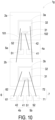
- FIG. 10 is a schematic view illustrating the structure of a switching module according to the eighth embodiment of the present disclosure.
- the switching module 1g includes two substrates, two switching elements, two first control parts 4a, 4b, two second control parts 5a, 5b, a first power part 6 and a second power part 7.
- the two substrates include a first substrate 2a and a second substrate 2b.
- the two switching elements include a first switching element 3a and a second switching element 3b.
- the first switching element 3a is disposed on the first substrate 2a.
- the second switching element 3b is disposed on the second substrate 2b.
- the first control part 4a is connected with the first control terminal 31 of the first switching element 3a.
- the first control part 4b is connected with the first control terminal 31 of the second switching element 3b.
- the second control part 5a is connected with the common conductive terminal 32 of the first switching element 3a.
- the second control part 5b is connected with the common conductive terminal 32 of the second switching element 3b.
- the first power part 6 is connected with the common conductive terminal 32 of the second switching element 3b.
- the second power part 7 is connected with the common conductive terminal 32 of the second switching element 3b.
- the first control part 4a and the second control part 5a are located at a first side of the second substrate 2b.
- the first control part 4a and the second control part 5a are arranged between the first substrate 2a and the second substrate 2b.
- the first power part 6, the first control part 4b, the second control part 5b and the second power part 7 are located at a second side of the second substrate 2b.
- the first side and the second side of the second substrate 2b are opposite to each other.
- the first power part 6, the first control part 4b, the second control part 5b and the second power part 7 are arranged sequentially.
- the switching module 1g further includes a first connecting conductor 101 and a second connecting conductor 102.
- the first connecting conductor 101 is connected between the common conductive terminal 32 of the first switching element 3a and the second substrate 2b.
- the second connecting conductor 102 is connected between the common conductive terminal 32 of the first switching element 3a and the second substrate 2b. Consequently, the first switching element 3a and the second switching element 3b are connected with each other in series.
- the first connecting conductor 101 and the second connecting conductor 102 are located at two opposite sides with respect to the first control part 4a and the second control part 5a. That is, the projections of the first connecting conductor 101 and the second connecting conductor 102 on the reference plane are located at the two opposite sides of the projections of the two control parts 4a and 5a on the reference plane, respectively. Consequently, the mutual inductance is reduced.
- the length of the first connecting conductor 101 and the length of the second connecting conductor 102 are equal. Consequently, the magnitude of the current flowing through the first connecting conductor 101 and the magnitude of the current flowing through the second connecting conductor 102 are equal. Since the first connecting conductor 101 and the second connecting conductor 102 are symmetric with respect to the control loop, the effect of cancelling out the magnetic fluxes is further improved. Consequently, the mutual inductance is further reduced.
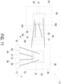
- FIG. 11 is a schematic view illustrating the structure of a switching module according to a ninth embodiment of the present disclosure.
- the structures and functions of the components of the switching module 1h which are identical to those of the eighth embodiment as shown in FIG. 10 are not redundantly described herein.
- the positions of the first switching element 3a, the first control part 4a and the second control part 5a of the switching module 1g are different.
- the first control part 4a and the second control part 5a are located at a third side of the second substrate 2b.
- the first control part 4a and the second control part 5a are arranged between the first substrate 2a and the second substrate 2b.
- the first power part 6, the first control part 4b, the second control part 5b and the second power part are located at the second side of the second substrate 2b.
- the first side and the second side of the second substrate 2b are opposite to each other.
- the third side of the second substrate 2b is arranged between the first side and the second side of the second substrate 2b.
- FIG. 12 schematically illustrates a first example of the relationship between the first control part, the second control part and the control loop of the switching module as shown in FIG. 1 .
- the center line O-O' of the control loop is defined by the first control part 4 and the second control part 5.
- the center line O-O' of the control loop passes through the center of the first control terminal 31 of the switching element 3 and a center of a line segment connecting the center of the first control pin 41 of the first control part 4 and the center of the second control pin 51 of the second control part 5.
- the smallest distance between the projection of the first power pin 61 of the first power part 6 on the reference plane and the center line O-O' of the control loop is defined as a first distance X1.
- the smallest distance between the projection of the second power pin 71 of the second power part 7 on the reference plane and the center line O-O' of the control loop is defined as a second distance X2.
- the minimum of the first distance X1 is 1mm
- the minimum of the second distance X2 is 1mm.
- the magnitude of the first current flowing through the first power part 6 and the magnitude of the second current flowing through the second power part 7 are equal, it is necessary to assure that the first power part 6 and the second power part 7 are symmetric with respect to the control loop of the first control part 4 and the second control part 5. If the first power part 6 and the second power part 7 are symmetric with respect to the control loop, the magnetic flux corresponding to the first current flowing through the first power part 6 and the magnetic flux corresponding to the second current flowing through the second power part 7 can be effectively cancelled out. Whether the first power part 6 and the second power part 7 are symmetric with respect to the control loop can be determined according to the asymmetry percentage of the first power part 6 and the second power part 7 with respect to the center line O-O' of the control loop.
- the asymmetry percentage of the first power part 6 and the second power part 7 with respect to the center line O-O' of the control loop is defined as the absolute value of the difference between the first distance X1 and the second distance X2 divided by the smaller one of the first distance X1 and the second distance X2. For example, if the first distance X1 is smaller than the second distance X2, the asymmetry percentage is expressed as (X2 - X1)/X1. Whereas, if the second distance X2 is smaller than the first distance X1, the asymmetry percentage is expressed as (X1-X2)/X2.
- a smaller asymmetry percentage indicates a better symmetry of the projection areas of the first power part 6 and the second power part 7 (on the reference plane) with respect to the center line O-O' of the control loop.
- a larger asymmetry percentage indicates a worse symmetry of the projections of the first power part 6 and the second power part 7 (on the reference plane) with respect to the center line O-O' of the control loop.
- the asymmetry percentage of the first power part 6 and the second power part 7 with respect to the center line O-O' of the control loop needs to be smaller than or equal to a predetermined asymmetry percentage (e.g., 60%, 40% or 20%). In case that the asymmetry percentage is 0%, the projections of the first power part 6 and the second power part 7 on the reference plane are completely symmetric with respect to the center line O-O' of the control loop.
- the asymmetry percentage is smaller than 40%, the mutual inductance between the first power part 6 (and the second power part 7) and the control loop is reduced and the switching speed of the switching module 1 is increased by 50%, basing on case of 100% asymmetry percentage. In case that the asymmetry percentage is further reduced, the switching speed of the switching module 1 is further increased.
- FIG. 13 schematically illustrates a second example of the relationship between the first control part, the second control part and the control loop of the switching module as shown in FIG. 1 .
- the magnitude of the first current P1 flowing through first power part 6 and the magnitude of the second current P2 flowing through the second power part 7 are different.
- the magnetic flux corresponding to the first current P1 flowing through the first power part 6 and the magnetic flux corresponding to the second current P2 flowing through the second power part 7 can be cancelled out.
- the first distance X1 is set to be greater than the second distance X2. Consequently, the magnetic flux corresponding to the first current P1 flowing through the first power part 6 and the magnetic flux corresponding to the second current P2 flowing through the second power part 7 can be cancelled out.
- the first distance X1 is set to be smaller than the second distance X2.
- the magnetic flux corresponding to the first current P1 flowing through the first power part 6 and the magnetic flux corresponding to the second current P2 flowing through the second power part 7 can also be cancelled out.
- the minimum of the first distance X1 is 1mm
- the minimum of the second distance X2 is 1mm.
- FIG. 14 is a schematic view illustrating the structure of a switching module according to a tenth embodiment of the present disclosure.
- the structures and functions of the components of the switching module 1i which are identical to those of the first embodiment as shown in FIG. 1 are not redundantly described herein.
- the switching module 1i of this embodiment further includes a third power part 8.
- the third power part 8, the first power part 6 and the second power part 7 are connected with the common conductive terminal 32 of the corresponding switching elements 3.
- the third power part 8 includes a third power pin 81 and a third power conductor 82.
- the third power pin 81 is disposed on the main circuit board.
- the third power conductor 82 is connected between the third power pin 81 and the common conductor terminal 32 of the corresponding switching element 3.
- a third current flows through the third power part 8.
- the direction of the first current, the direction of the second current and the direction of the third current are identical.
- the first current, the second current and the third current flow from the common conductive terminal 32 of the switching module 1i to the corresponding power pins.
- the second power part 7 and the third power part 8 are located at the same side with respect to the control loop, and the second power part 7 and the first power part 6 are located at opposite sides with respect to the control loop.
- the direction of the magnetic flux through the control loop corresponding to the second current flowing through the second power part 7 and the direction of the magnetic flux through the control loop corresponding to the third current flowing through the third power part 8 are identical, and the direction of the magnetic flux through the control loop corresponding to the second current flowing through the second power part 7 and the direction of the magnetic flux through the control loop corresponding to the first current flowing through the first power part 6 are opposite.
- the smallest distance between the projection of the first power pin 61 on the reference plane and the center line O-O' of the control loop is defined as a first distance X1.
- the smallest distance between the projection of the second power pin 71 on the reference plane and the center line O-O' of the control loop is defined as a second distance X2.
- the smallest distance between the projection of the third power pin 81 on the reference plane and the center line O-O' of the control loop is defined as a third distance.
- the first distance X1 is equal to the second distance X2. Since the third distance is much longer than the first distance X1 and the second distance X2, the magnetic flux corresponding to the third current flowing through the third power part 8 has small influence on the control loop. Consequently, the purpose of cancelling out the magnetic fluxes can be achieved.
- the switching module includes a plurality of third power parts 8.
- the plurality of third power parts 8 are located at the same side of the control loop.
- some of the third power parts 8 are located at a first side of the control loop, and the others of the third power parts 8 are located at a second side of the control loop.
- the number of the third power parts 8 at the first side of the control loop and the number of the third power parts 8 at a second side of the control loop should be specially designed.
- the sum of the numbers of the first power part 6 and the third power part 8 located at one side of the control loop is defined as the first number
- the sum of the numbers of the second power part 7 and the third power part 8 located at the other side of the control loop is defined as the second number.
- the absolute value of the difference between the first number and the second number is smaller than or equal to 3.
- the direction of the first current flowing through the first power part and the direction of the second current flowing through the second power part are identical.
- the projection of the first power part on the reference plane and the projection of the second power part on the reference plane are located at two sides of the control loop of the switching module. Consequently, the mutual inductance of the control loop is reduced, and the safety performance of the switching module is enhanced.
Landscapes
- Engineering & Computer Science (AREA)
- Power Engineering (AREA)
- Physics & Mathematics (AREA)
- Electromagnetism (AREA)
- Power Conversion In General (AREA)
- Direct Current Feeding And Distribution (AREA)
- Inverter Devices (AREA)
Abstract
Description
- The present disclosure relates to a switching module, and more particularly to a switching module for reducing the mutual inductance between a power loop and a control loop.
- Generally, a switching module of a power electronic system operates at a high frequency to achieve high power density. However, the high operating frequency may increase the switching loss, and thus reduce the efficiency of the switching module. Consequently, when the switching module operates at the high frequency, it is necessary to increase the switching speed of the switching module in order to reduce the switching loss. However, when the switching module operates at the higher switching speed, a serious electromagnetic interference (EMI) problem occurs.
- Especially, in case that the switching module has a high power density structure, the power loop is relatively close to the control loop. When the current in the power loop changes, the induced magnetic field also changes around the power loop. As the induced magnetic field passes through the control loop, a corresponding induced voltage is generated in the control loop. Consequently, the electromagnetic interference of the mutual inductance between the power loop and the control loop is formed, which affects the switching operation of the switching module.
- In the conventional switching module, a plurality of power loops are located beside each other, and a plurality of control loops are located beside each other. In other words, no control loop is arranged between every two adjacent power loops, and no power loop is arranged between every two adjacent control loops. Consequently, the induced magnetic fields generated by the power loops pass through the control loops in the same direction. Under this circumstance, the electromagnetic interference of the mutual inductance between the power loops and the control loops is largely increased. If the electromagnetic interference of the mutual inductance is too large, the interference voltage at a control terminal of the switching module may exceed the safe range. Under this circumstance, the reliability of the switching module is reduced, and the switching module is even unable to work normally.
- Therefore, there is a need of providing an improved switching module in order to overcome the drawbacks of the conventional technologies.
- The present disclosure provides a switching module for reducing the mutual inductance between a power loop and a control loop.
- In accordance with an aspect of the present disclosure, a switching module is provided. The switching module includes at least one substrate, at least one switching element, at least one control loop, a first power part and a second power part. The at least one switching element is disposed on the at least one substrate. The at least one control loop is connected with the corresponding switching element. The first power part is connected with the corresponding switching element. The second power part is connected with the corresponding switching element. A direction of a first current flowing through the first power part and a direction of a second current flowing through the second power part are identical. A projection of the first power part on a reference plane and a projection of the second power part on the reference plane are located at two opposite sides of a projection of the control loop on the reference plane.
- The above contents of the present disclosure will become more readily apparent to those ordinarily skilled in the art after reviewing the following detailed description and accompanying drawings, in which:
-
-
FIG. 1 is a schematic view illustrating the structure of a switching module according to a first embodiment of the present disclosure; -
FIG. 2 is a schematic side view illustrating a portion of the switching module as shown inFIG. 1 and taken along the section A-A'; -
FIG. 3 schematically illustrates the magnetic flux cancellation principle for the switching module as shown inFIG. 1 ; -
FIG. 4 is a schematic view illustrating the structure of a switching module according to a second embodiment of the present disclosure; -
FIG. 5A is a schematic view illustrating the structure of a switching module according to a third embodiment of the present disclosure; -
FIG. 5B is a schematic circuit diagram of the switching module as shown inFIG. 5A ; -
FIG. 6 is a schematic view illustrating the structure of a switching module according to a fourth embodiment of the present disclosure; -
FIG. 7 is a schematic view illustrating the structure of a switching module according to a fifth embodiment of the present disclosure; -
FIG. 8 is a schematic view illustrating the structure of a switching module according to a sixth embodiment of the present disclosure; -
FIG. 9 is a schematic view illustrating the structure of a switching module according to a seventh embodiment of the present disclosure; -
FIG. 10 is a schematic view illustrating the structure of a switching module according to the eighth embodiment of the present disclosure; -
FIG. 11 is a schematic view illustrating the structure of a switching module according to a ninth embodiment of the present disclosure; -
FIG. 12 schematically illustrates a first example of the relationship between the first control part, the second control part and the control loop of the switching module as shown inFIG. 1 ; -
FIG. 13 schematically illustrates a second example of the relationship between the first control part, the second control part and the control loop of the switching module as shown inFIG. 1 ; and -
FIG. 14 is a schematic view illustrating the structure of a switching module according to a tenth embodiment of the present disclosure. - The present disclosure will now be described more specifically with reference to the following embodiments. It is to be noted that the following descriptions of preferred embodiments of this disclosure are presented herein for purpose of illustration and description only. It is not intended to be exhaustive or to be limited to the precise form disclosed.
- Please refer to
FIGS. 1 ,2 and3 .FIG. 1 is a schematic view illustrating the structure of a switching module according to a first embodiment of the present disclosure.FIG. 2 is a schematic side view illustrating a portion of the switching module as shown inFIG. 1 and taken along the section A-A'.FIG. 3 schematically illustrates the magnetic flux cancellation principle for the switching module as shown inFIG. 1 . - In an embodiment, the
switching module 1 is disposed on a main circuit board (not shown) and electrically connected with the main circuit board. Theswitching module 1 includes asubstrate 2, aswitching element 3, afirst control part 4, asecond control part 5, afirst power part 6 and asecond power part 7. - In an embodiment, the
switching element 3 is a vertical-type device. Preferably but not exclusively, theswitching element 3 is an insulated gate bipolar transistor (IGBT), a bipolar junction transistor (BJT), a metal-oxide-semiconductor field-effect transistor (MOSFET), a junction field effect transistor (JFET) or a gallium nitride high electron mobility transistor (GaN-HEMT). - As shown in
FIG. 2 , theswitching element 3 is welded on thesubstrate 2 through a connectingmaterial 11. Theswitching element 3 includes afirst control terminal 31, a second control terminal, a first power terminal and asecond power terminal 33. Thefirst control terminal 31, the second control terminal and the first power terminal are disposed on afirst surface 34 of theswitching element 3. Since the second control terminal and the first power terminal are located at the same region of theswitching element 3, the second control terminal and the first power terminal are also referred as a commonconductive terminal 32. Thesecond power terminal 33 is disposed on asecond surface 35 of theswitching element 3. Thesecond power terminal 33 is connected with thesubstrate 2 through the connectingmaterial 11. - In some embodiments, in case that the switching
element 3 is an insulated gate bipolar transistor (IGBT), thefirst control terminal 31 is served as a gate terminal of theswitching element 3, the common conductive terminal 32 (i.e., the second control terminal and the first power terminal) is served as an emitter of theswitching element 3, and thesecond power terminal 33 is served as a collector of theswitching element 3. In some other embodiments, in case that the switchingelement 3 is a bipolar junction transistor (BJT), thefirst control terminal 31 is served as a base of theswitching element 3, the common conductive terminal 32 (i.e., the second control terminal and the first power terminal) is served as an emitter of theswitching element 3, and thesecond power terminal 33 is served as a collector of theswitching element 3. In some other embodiments, in case that the switchingelement 3 is a metal-oxide-semiconductor field-effect transistor (MOSFET), a junction field effect transistor (JFET) or a gallium nitride high electron mobility transistor (GaN-HEMT), thefirst control terminal 31 is served as a gate terminal of theswitching element 3, the common conductive terminal 32 (i.e., the second control terminal and the first power terminal) is served as a source terminal of theswitching element 3, and thesecond power terminal 33 is served as a drain terminal of theswitching element 3. - Please refer to
FIG. 1 again. Thefirst control part 4 is connected with thefirst control terminal 31 of theswitching element 3. Thefirst control part 4 includes afirst control pin 41 and afirst control conductor 42. Thefirst control pin 41 is disposed on the main circuit board. Thefirst control conductor 42 is connected between thefirst control pin 41 and thefirst control terminal 31 of theswitching element 3. Thesecond control part 5 is connected with the second control terminal (i.e., the common conductive terminal 32) of theswitching element 3. Thesecond control part 5 includes asecond control pin 51 and asecond control conductor 52. Thesecond control pin 51 is disposed on the main circuit board. Thesecond control conductor 52 is connected between thesecond control pin 51 and the second control terminal (i.e., the common conductive terminal 32) of theswitching element 3. Moreover, a control loop of theswitching module 1 is defined by the second control terminal (i.e., the common conductive terminal 32), thesecond control conductor 52, thesecond control pin 51, the main circuit board, thefirst control pin 41, thefirst control conductor 42 and thefirst control terminal 31 collaboratively. - The
first power part 6 is connected with the first power terminal (i.e., the common conductive terminal 32) of theswitching element 3. Thefirst power part 6 includes afirst power pin 61 and afirst power conductor 62. Thefirst power pin 61 is disposed on the main circuit board. Thefirst power conductor 62 is connected between thefirst power pin 61 and the first power terminal (i.e., the common conductive terminal 32) of theswitching element 3. A first current flows through thefirst power part 6. Thesecond power part 7 is connected with the first power terminal (i.e., the common conductive terminal 32) of theswitching element 3. Thesecond power part 7 includes asecond power pin 71 and asecond power conductor 72. Thesecond power pin 71 is disposed on the main circuit board. Thesecond power conductor 72 is connected between thesecond power pin 71 and the first power terminal (i.e., the common conductive terminal 32) of theswitching element 3. A second current flows through thesecond power part 7. - It is noted that the switching
element 3 corresponding to thefirst power part 6 and theswitching element 3 corresponding to thesecond power part 7 may be the identical ordifferent switching elements 3. In other words, thefirst power part 6 and thesecond power part 7 may be connected with thesame switching element 3 or respectively connected with twodifferent switching elements 3. In this embodiment, the direction of the first current flowing through thefirst power part 6 and the direction of the second current flowing through thesecond power part 7 are identical. That is, the first current flows from the first power terminal (i.e., the common conductive terminal 32) to thefirst power pin 61 of thefirst power part 6 and the second current flows from the first power terminal (i.e., the common conductive terminal 32) to thesecond power pin 71 of thesecond power part 7, or the first current flows from thefirst power pin 61 of thefirst power part 6 to the first power terminal (i.e., the common conductive terminal 32) and the second current flows from thesecond power pin 71 of thesecond power part 7 to the first power terminal (i.e., the common conductive terminal 32). It is noted that numerous modifications and alterations may be made while retaining the teachings of the disclosure. For example, in another embodiment, thefirst power part 6 and thesecond power part 7 are connected with thesecond power terminal 33 of thecorresponding switching element 3. However, the direction of the first current flowing through thefirst power part 6 and the direction of the second current flowing through thesecond power part 7 are identical. - In this embodiment, the
first power part 6, thefirst control part 4, thesecond control part 5 and thesecond power part 7 are arranged sequentially. The projection of thefirst power part 6 on a reference plane and a projection of thesecond power part 7 on the same reference plane are located at two sides of a projection of the control loop of the switching module 1 (i.e., the control loop defined by thefirst control part 4 and the second control part 5) on the reference plane. Preferably, the reference plane is coplanar with thesubstrate 2. In an embodiment, the length of thefirst power part 6 is equal to the length of thesecond power part 7. Consequently, the current value of the first current flowing through thefirst power part 6 and the current value of the second current flowing through thesecond power part 7 are equal. Under this circumstance, the current value here refers to the amplitude of the corresponding current or the effective value of the corresponding current. - In
FIG. 3 , the projections of thefirst power part 6, thesecond power part 7 and the control loop on the reference plane are shown. The point A and the point B as shown inFIG. 3 denote two ends of the projection of thefirst control part 4 on the reference plane, respectively. The point C and the point D as shown inFIG. 3 denote two ends of the projection of thesecond control part 5 on the reference plane, respectively. Moreover, the line P1 denotes the first current flowing through thefirst power part 6, and the line P2 denotes the second current flowing through thesecond power part 7. In the embodiment, the point B and the point D are connected with each other through the main circuit board. Consequently, the rectangular region defined by the points A, B, C and D represents the projection of the control loop on the reference plane. The line O-O' represents the center line of the control loop on the reference plane. That is, the center line O-O' passes through the midpoint of a line segment connecting the point A and the point C, and the midpoint of a line segment connecting the point B and the point D. The projection of thefirst power part 6 on the reference plane and the projection of thesecond power part 7 on the reference plane are located at two sides of the projection of the control loop on the reference plane, respectively. For example, the first current P1 flowing through thefirst power part 6 and the second current P2 flowing through thesecond power part 7 are symmetrical the two sides of the projection of the control loop on the reference plane. Preferably but not exclusively, the distance between the projection of thefirst power part 6 on the reference plane and the center line O-O' is equal to the distance between the projection of thesecond power part 7 on the reference plane and the center line O-O'. For example, it can be set that the smallest distance between the projection of thefirst power part 6 on the reference plane and the center line O-O' is 1mm, and the smallest distance between the projection of thesecond power part 7 on the reference plane and the center line O-O' is 1mm. The first current P1 flowing through thefirst power part 6 produces a total magnetic flux Φ1 through the control loop. The second current P2 flowing through thesecond power part 7 produces a total magnetic flux Φ2 through the control loop. Since the direction of the first current P1 and the direction of the second current P2 are identical, the magnitude of the magnetic flux Φ1 and the magnitude of the magnetic flux Φ2 are equal, but the direction of the magnetic flux Φ1 and the direction of the magnetic flux Φ2 are opposite. In other words, the direction of the magnetic flux induced by the first current P1 through the control loop is perpendicular to the paper surface and inward, and the direction of the magnetic flux induced by the second current P2 through the control loop is perpendicular to the paper surface and outward. The magnetic flux Φ1 and the magnetic flux Φ2 are cancelled out. Consequently, the overall mutual inductance between thefirst power part 6, thesecond power part 7 and the control loop is largely reduced. - As mentioned above, the direction of the first current P1 flowing through the
first power part 6 and the direction of the second current P2 flowing through thesecond power part 7 are identical. In addition, the projection of thefirst power part 6 on the reference plane and the projection of thesecond power part 7 on the same reference plane are located at two sides of the projection of the control loop of theswitching module 1 on the reference plane. In comparison with the conventional switching module, the mutual inductance between the power loop and the control loop in theswitching module 1 of the present disclosure is reduced. Consequently, the safety performance of theswitching module 1 is enhanced. - As mentioned above, the direction of the first current P1 and the direction of the second current P2 are identical. That is, the direction of the first current P1 and the direction of the second current P2 are in parallel with each other. It is noted that the direction of the first current P1 and the direction of the second current P2 are not restricted to be in parallel with each other. For example, in some embodiments, there is an angle between the direction of the first current P1 and the direction of the second current P2. The angle is smaller than 90 degrees. Particularly, after the
first power part 6 and thesecond power part 7 are projected to a reference plane, the angle between first current P1 and the second current P2 is 0 degree or an acute angle. The reference plane is a plane coplanar with thesubstrate 2 or a plane that is perpendicular to thesubstrate 2 and passes through the center line O-O'. - In some embodiments, the direction of the first current P1 and the direction of the second current P2 are identical, but the
first power part 6 and thesecond power part 7 are not completely symmetric with respect to the control loop or the magnitude of the first current P1 and the magnitude of the second current P2 are different. Since the direction of the magnetic flux Φ1 corresponding to the first current P1 and the direction of the magnetic flux Φ2 corresponding to the second current P2 are opposite, the magnetic flux Φ1 and the magnetic flux Φ2 are cancelled out. Consequently, the overall mutual inductance between thefirst power part 6, thesecond power part 7 and the control loop is largely reduced. - In some embodiments, the direction of the first current P1 flowing through the
first power part 6 and the direction of the second current P2 flowing through thesecond power part 7 are in parallel with each other or tilted respective to each other. As long as the magnetic flux Φ1 corresponding to the first current P1 and the magnetic flux Φ2 corresponding to the second current P2 can be cancelled out and the mutual inductance is reduced, the installation positions of thefirst power part 6 and thesecond power part 7 are not restricted. - Please refer to
FIG. 4. FIG. 4 is a schematic view illustrating the structure of a switching module according to a second embodiment of the present disclosure. The structures and functions of the components of theswitching module 1a which are identical to those of the first embodiment as shown inFIG. 1 are not redundantly described herein. In comparison with theswitching module 1, theswitching module 1a of this embodiment further includes afourth power part 9. Thefirst power part 6 and thesecond power part 7 of theswitching module 1a are connected with thesecond power terminal 33 of thecorresponding switching element 3 through thesubstrate 2. Thefourth power part 9 is connected with the commonconductive terminal 32 of thecorresponding switching element 3. Thefourth power part 9 includes afourth power pin 91 and thefourth power conductor 92. Thefourth power pin 91 is disposed on the main circuit board. Thefourth power conductor 92 is connected between thefourth power pin 91 and the commonconductive terminal 32 of thecorresponding switching element 3. - In this embodiment, the projection of the
substrate 2 on the reference plane is a square with four sides. The projections of thefirst power part 6 and thesecond power part 7 are located at the same side with respect to the projection of thesubstrate 2. The projection of thefourth power part 9 and the projection of the first power part 6 (or the second power part 7) are located at different sides of the projection of thesubstrate 2. For example, the projections of thefirst power part 6 and thesecond power part 7 are located at a first side of the projection of thesubstrate 2, and the projection of thefourth power part 9 is located at a second side of the projection of thesubstrate 2. In an embodiment, the first side and the second side of the projection of thesubstrate 2 are opposite to each other. In another embodiment, the first side and the second side of the projection of thesubstrate 2 are adjacent to each other. - Please refer to
FIGS. 5A and5B .FIG. 5A is a schematic view illustrating the structure of a switching module according to a third embodiment of the present disclosure.FIG. 5B is a schematic circuit diagram of the switching module as shown inFIG. 5A . The structures and functions of the components of theswitching module 1b which are identical to those of the first embodiment as shown inFIG. 1 are not redundantly described herein. The switchingelement 3 of theswitching module 1 as shown inFIG. 1 has a vertical-type structure. In this embodiment, the switchingelement 3 of theswitching module 1b is a planar switching element. That is, thesecond power terminal 33, thefirst control terminal 31 and the common conductive terminal 32 are disposed on thefirst surface 34 of theswitching element 3. Thefirst power part 6 and thesecond power part 7 are connected with the commonconductive terminal 32. Thefourth power part 9 is connected with thesecond power terminal 33. -
FIG. 6 is a schematic view illustrating the structure of a switching module according to a fourth embodiment of the present disclosure. The structures and functions of the components of theswitching module 1c which are identical to those of the first embodiment as shown inFIG. 1 are not redundantly described herein. In this embodiment, theswitching module 1c includes two switching elements (i.e., afirst switching element 3a and asecond switching element 3b), twofirst control parts 4, twosecond control parts 5, afirst power parts 6 and asecond power part 7. Thefirst switching element 3a and thesecond switching element 3b are connected with each other in parallel. One of the twofirst control parts 4 is connected with thefirst control terminal 31 of thefirst switching element 3a. The other of the twofirst control parts 4 is connected with thefirst control terminal 31 of thesecond switching element 3b. One of the twosecond control parts 5 is connected with the commonconductive terminal 32 of thefirst switching element 3a. The other of thesecond control parts 5 is connected with the commonconductive terminal 32 of thesecond switching element 3b. - The
first power part 6 is connected with the commonconductive terminal 32 of thefirst switching element 3a. Thesecond power part 7 is connected with the commonconductive terminal 32 of thesecond switching element 3b. In this embodiment, thefirst power part 6, thesecond control part 5 connected with thefirst switching element 3a, thefirst control part 4 connected with thefirst switching element 3a, thefirst control part 4 connected with thesecond switching element 3b, thesecond control part 5 connected with thesecond switching element 3b and thesecond power part 7 are arranged sequentially. - In this embodiment, a first control loop of the
switching module 1c is defined by the commonconductive terminal 32 of thefirst switching element 3a, the correspondingsecond control conductor 52, thesecond control pin 51, the main circuit board, thefirst control pin 41, the correspondingfirst control conductor 42 and thefirst control terminal 31 of thefirst switching element 3a collaboratively. In addition, a second control loop of theswitching module 1c is defined by the commonconductive terminal 32 of thesecond switching element 3b, the correspondingsecond control conductor 52, the correspondingsecond control pin 51, the main circuit board, thefirst control pin 41, thefirst control conductor 42 and thefirst control terminal 31 of thesecond switching element 3b collaboratively. In this embodiment, the direction of the first current flowing through thefirst power part 6 and the direction of the second current flowing through thesecond power part 7 are identical. That is, the first current flows from the common conductive terminal 32 to thefirst power pin 61 of thefirst power part 6 and the second current flows from the common conductive terminal 32 to thesecond power pin 71 of thesecond power part 7, or the first current flows from thefirst power pin 61 of thefirst power part 6 to the commonconductive terminal 32 and the second current flows from thesecond power pin 71 of thesecond power part 7 to the commonconductive terminal 32. The magnetic flux through the first control loop and the second control loop induced by the first current flowing through thefirst power part 6 and the magnetic flux through the first control loop and the second control loop induced by the second current flowing through thesecond power part 7 are cancelled out. Consequently, the overall mutual inductance between thefirst power part 6, thesecond power part 7 and the first control loop and/or the second control loop is largely reduced. In this way, the reliability of theswitching elements 1c is increased. -
FIG. 7 is a schematic view illustrating the structure of a switching module according to a fifth embodiment of the present disclosure. The structures and functions of the components of the switching module Id which are identical to those of the fourth embodiment as shown inFIG. 6 are not redundantly described herein. In comparison with theswitching module 1c ofFIG. 6 , the switching module Id includes three switching elements (i.e., afirst switching element 3a, asecond switching element 3b and athird switching element 3c), threefirst control parts 4, threesecond control parts 5, afirst power parts 6 and asecond power part 7. Thethird switching element 3c is arranged between thefirst switching element 3a and thesecond switching element 3b. Thefirst switching element 3a, thesecond switching element 3b and thethird switching element 3c are connected with each other in parallel. The additionalfirst control part 4 is connected with thefirst control terminal 31 of thethird switching element 3c. The additionalsecond control part 5 is connected with the commonconductive terminal 32 of thethird switching element 3c. - In this embodiment, the switching module Id further includes a
third power part 8. Thethird power part 8 is connected with the commonconductive terminal 32 of thethird switching element 3c. Thethird power part 8 includes athird power pin 81 and thethird power conductor 82. Thethird power pin 81 is disposed on the main circuit board. Thethird power conductor 82 is connected between thethird power pin 81 and the commonconductive terminal 32 of thethird switching element 3c. A third current flows through thethird power part 8. The direction of the third current, the direction of the first current flowing through thefirst power part 6 and the direction of the second current flowing through thesecond power part 7 are identical. In this embodiment, thefirst power part 6, thesecond control part 5 connected with thefirst switching element 3a, thefirst control part 4 connected with thefirst switching element 3a, thethird power part 8, thesecond control part 5 connected with thethird switching element 3c, thefirst control part 4 connected with thethird switching element 3c, thefirst control part 4 connected with thesecond switching element 3b, thesecond control part 5 connected with thesecond switching element 3b and thesecond power part 7 are arranged sequentially. It is noted that the position of thethird power part 8 is not restricted. For example, in another embodiment, thefirst power part 6, thesecond control part 5 connected with thefirst switching element 3a, thefirst control part 4 connected with thefirst switching element 3a, thesecond control part 5 connected with thethird switching element 3c, thefirst control part 4 connected with thethird switching element 3c, thethird power part 8, thefirst control part 4 connected with thesecond switching element 3b, thesecond control part 5 connected with thesecond switching element 3b and thesecond power part 7 are arranged sequentially. - In this embodiment, the direction of the first current flowing through the
first power part 6, the direction of the second current flowing through thesecond power part 7 and the direction of the third current flowing through thethird power part 8 are identical. Consequently, the mutual inductance between thefirst power part 6, thesecond power part 7 and the control loops is largely reduced, and the mutual inductance between thesecond power part 7, thethird power part 8 and the control loops is largely reduced. Since the interference of the high-frequency control signal is avoided, the reliability of theswitching elements 1d is increased. -
FIG. 8 is a schematic view illustrating the structure of a switching module according to a sixth embodiment of the present disclosure. The structures and functions of the components of theswitching module 1e which are identical to those of the fifth embodiment as shown inFIG. 7 are not redundantly described herein. In comparison with theswitching module 1d ofFIG. 7 , theswitching module 1e further includes a third connecting conductor 103. The third connecting conductor 103 is connected between thefirst control terminal 31 of thesecond switching element 3b and thefirst control terminal 31 of thethird switching element 3c. Consequently, onefirst control part 4 is shared by thesecond switching element 3b and thethird switching element 3c of theswitching module 1e. Since thefirst control part 4 connected with thethird switching element 3c is shared by thesecond switching element 3b and thethird switching element 3c, thefirst control part 4 connected with thesecond switching element 3b as shown inFIG. 7 is omitted in theswitching module 1e of this embodiment. It is noted that numerous modifications and alterations may be made while retaining the teachings of the disclosure. For example, in another embodiment, onesecond control part 5 is shared by thesecond switching element 3b and thethird switching element 3c of theswitching module 1e. In addition, a connecting conductor is connected between the commonconductive terminal 32 of thesecond switching element 3b and the commonconductive terminal 32 of thethird switching element 3c. In some other embodiments, the number of switching elements sharing the same control part is not restricted to two. That is, the number of switching elements sharing the same control part may be increased according to the practical requirements. -
FIG. 9 is a schematic view illustrating the structure of a switching module according to a seventh embodiment of the present disclosure. The structures and functions of the components of the switching module If which are identical to those of the first embodiment as shown inFIG. 1 are not redundantly described herein. In comparison with theswitching module 1 as shown inFIG. 1 , the switching module If further includes adiode 10, a first connectingconductor 101 and a second connectingconductor 102. Thediode 10 is disposed on thesubstrate 2. The first connectingconductor 101 is connected between a terminal of thediode 10 and thecommon conductor terminal 32 of theswitching element 3. In addition, the first connectingconductor 101 is connected with thefirst power conductor 62 of thefirst power part 6. The second connectingconductor 102 is connected between the same terminal of thediode 10 and thecommon conductor terminal 32 of theswitching element 3. In addition, the second connectingconductor 102 is connected with thesecond power conductor 72 of thesecond power part 7. Similarly, the projections of the first connectingconductor 101 and the second connectingconductor 102 on the reference plane are symmetrically located at two opposite sides of the projections of twocontrol parts conductors -
FIG. 10 is a schematic view illustrating the structure of a switching module according to the eighth embodiment of the present disclosure. The structures and functions of the components of theswitching module 1g which are identical to those of the first embodiment as shown inFIG. 1 are not redundantly described herein. In comparison with theswitching module 1 as shown inFIG. 1 , theswitching module 1g includes two substrates, two switching elements, twofirst control parts second control parts first power part 6 and asecond power part 7. The two substrates include afirst substrate 2a and asecond substrate 2b. The two switching elements include afirst switching element 3a and asecond switching element 3b. - The
first switching element 3a is disposed on thefirst substrate 2a. Thesecond switching element 3b is disposed on thesecond substrate 2b. Thefirst control part 4a is connected with thefirst control terminal 31 of thefirst switching element 3a. Thefirst control part 4b is connected with thefirst control terminal 31 of thesecond switching element 3b. Thesecond control part 5a is connected with the commonconductive terminal 32 of thefirst switching element 3a. Thesecond control part 5b is connected with the commonconductive terminal 32 of thesecond switching element 3b. - The
first power part 6 is connected with the commonconductive terminal 32 of thesecond switching element 3b. Thesecond power part 7 is connected with the commonconductive terminal 32 of thesecond switching element 3b. In this embodiment, thefirst control part 4a and thesecond control part 5a are located at a first side of thesecond substrate 2b. In addition, thefirst control part 4a and thesecond control part 5a are arranged between thefirst substrate 2a and thesecond substrate 2b. Thefirst power part 6, thefirst control part 4b, thesecond control part 5b and thesecond power part 7 are located at a second side of thesecond substrate 2b. The first side and the second side of thesecond substrate 2b are opposite to each other. In this embodiment, thefirst power part 6, thefirst control part 4b, thesecond control part 5b and thesecond power part 7 are arranged sequentially. - In this embodiment, the
switching module 1g further includes a first connectingconductor 101 and a second connectingconductor 102. The first connectingconductor 101 is connected between the commonconductive terminal 32 of thefirst switching element 3a and thesecond substrate 2b. The second connectingconductor 102 is connected between the commonconductive terminal 32 of thefirst switching element 3a and thesecond substrate 2b. Consequently, thefirst switching element 3a and thesecond switching element 3b are connected with each other in series. - Preferably, the first connecting
conductor 101 and the second connectingconductor 102 are located at two opposite sides with respect to thefirst control part 4a and thesecond control part 5a. That is, the projections of the first connectingconductor 101 and the second connectingconductor 102 on the reference plane are located at the two opposite sides of the projections of the twocontrol parts conductor 101 and the length of the second connectingconductor 102 are equal. Consequently, the magnitude of the current flowing through the first connectingconductor 101 and the magnitude of the current flowing through the second connectingconductor 102 are equal. Since the first connectingconductor 101 and the second connectingconductor 102 are symmetric with respect to the control loop, the effect of cancelling out the magnetic fluxes is further improved. Consequently, the mutual inductance is further reduced. -
FIG. 11 is a schematic view illustrating the structure of a switching module according to a ninth embodiment of the present disclosure. The structures and functions of the components of theswitching module 1h which are identical to those of the eighth embodiment as shown inFIG. 10 are not redundantly described herein. In comparison with theswitching module 1g as shown inFIG. 10 , the positions of thefirst switching element 3a, thefirst control part 4a and thesecond control part 5a of theswitching module 1g are different. Thefirst control part 4a and thesecond control part 5a are located at a third side of thesecond substrate 2b. In addition, thefirst control part 4a and thesecond control part 5a are arranged between thefirst substrate 2a and thesecond substrate 2b. Thefirst power part 6, thefirst control part 4b, thesecond control part 5b and the second power part are located at the second side of thesecond substrate 2b. The first side and the second side of thesecond substrate 2b are opposite to each other. In addition, the third side of thesecond substrate 2b is arranged between the first side and the second side of thesecond substrate 2b. -
FIG. 12 schematically illustrates a first example of the relationship between the first control part, the second control part and the control loop of the switching module as shown inFIG. 1 . As mentioned above, the center line O-O' of the control loop is defined by thefirst control part 4 and thesecond control part 5. As shown inFIG. 12 , the center line O-O' of the control loop passes through the center of thefirst control terminal 31 of theswitching element 3 and a center of a line segment connecting the center of thefirst control pin 41 of thefirst control part 4 and the center of thesecond control pin 51 of thesecond control part 5. The smallest distance between the projection of thefirst power pin 61 of thefirst power part 6 on the reference plane and the center line O-O' of the control loop is defined as a first distance X1. The smallest distance between the projection of thesecond power pin 71 of thesecond power part 7 on the reference plane and the center line O-O' of the control loop is defined as a second distance X2. In some embodiments, the minimum of the first distance X1 is 1mm, and the minimum of the second distance X2 is 1mm. - In case that the magnitude of the first current flowing through the
first power part 6 and the magnitude of the second current flowing through thesecond power part 7 are equal, it is necessary to assure that thefirst power part 6 and thesecond power part 7 are symmetric with respect to the control loop of thefirst control part 4 and thesecond control part 5. If thefirst power part 6 and thesecond power part 7 are symmetric with respect to the control loop, the magnetic flux corresponding to the first current flowing through thefirst power part 6 and the magnetic flux corresponding to the second current flowing through thesecond power part 7 can be effectively cancelled out. Whether thefirst power part 6 and thesecond power part 7 are symmetric with respect to the control loop can be determined according to the asymmetry percentage of thefirst power part 6 and thesecond power part 7 with respect to the center line O-O' of the control loop. - The asymmetry percentage of the
first power part 6 and thesecond power part 7 with respect to the center line O-O' of the control loop is defined as the absolute value of the difference between the first distance X1 and the second distance X2 divided by the smaller one of the first distance X1 and the second distance X2. For example, if the first distance X1 is smaller than the second distance X2, the asymmetry percentage is expressed as (X2 - X1)/X1. Whereas, if the second distance X2 is smaller than the first distance X1, the asymmetry percentage is expressed as (X1-X2)/X2. - A smaller asymmetry percentage indicates a better symmetry of the projection areas of the
first power part 6 and the second power part 7 (on the reference plane) with respect to the center line O-O' of the control loop. A larger asymmetry percentage indicates a worse symmetry of the projections of thefirst power part 6 and the second power part 7 (on the reference plane) with respect to the center line O-O' of the control loop. - As mentioned above, if the magnetic flux corresponding to the first current P1 flowing through the
first power part 6 and the magnetic flux corresponding to the second current P2 flowing through thesecond power part 7 are cancelled out, the mutual inductance between the first power part 6 (and the second power part 7) and the control loop is reduced. For achieving this purpose, the asymmetry percentage of thefirst power part 6 and thesecond power part 7 with respect to the center line O-O' of the control loop needs to be smaller than or equal to a predetermined asymmetry percentage (e.g., 60%, 40% or 20%). In case that the asymmetry percentage is 0%, the projections of thefirst power part 6 and thesecond power part 7 on the reference plane are completely symmetric with respect to the center line O-O' of the control loop. When the asymmetry percentage is smaller than 40%, the mutual inductance between the first power part 6 (and the second power part 7) and the control loop is reduced and the switching speed of theswitching module 1 is increased by 50%, basing on case of 100% asymmetry percentage. In case that the asymmetry percentage is further reduced, the switching speed of theswitching module 1 is further increased. - Please refer to
FIGS. 1 ,12 and13. FIG. 13 schematically illustrates a second example of the relationship between the first control part, the second control part and the control loop of the switching module as shown inFIG. 1 . In this embodiment, the magnitude of the first current P1 flowing throughfirst power part 6 and the magnitude of the second current P2 flowing through thesecond power part 7 are different. By adjusting the first distance X1 and the second distance X2, the magnetic flux corresponding to the first current P1 flowing through thefirst power part 6 and the magnetic flux corresponding to the second current P2 flowing through thesecond power part 7 can be cancelled out. In case that the magnitude of the first current P1 flowing throughfirst power part 6 is greater than the magnitude of the second current P2 flowing through thesecond power part 7, the first distance X1 is set to be greater than the second distance X2. Consequently, the magnetic flux corresponding to the first current P1 flowing through thefirst power part 6 and the magnetic flux corresponding to the second current P2 flowing through thesecond power part 7 can be cancelled out. Whereas, in case that the magnitude of the first current P1 flowing throughfirst power part 6 is lower than the magnitude of the second current P2 flowing through thesecond power part 7, the first distance X1 is set to be smaller than the second distance X2. Consequently, the magnetic flux corresponding to the first current P1 flowing through thefirst power part 6 and the magnetic flux corresponding to the second current P2 flowing through thesecond power part 7 can also be cancelled out. In an embodiment, the minimum of the first distance X1 is 1mm, and the minimum of the second distance X2 is 1mm. -
FIG. 14 is a schematic view illustrating the structure of a switching module according to a tenth embodiment of the present disclosure. The structures and functions of the components of theswitching module 1i which are identical to those of the first embodiment as shown inFIG. 1 are not redundantly described herein. In comparison with theswitching module 1, theswitching module 1i of this embodiment further includes athird power part 8. Thethird power part 8, thefirst power part 6 and thesecond power part 7 are connected with the commonconductive terminal 32 of thecorresponding switching elements 3. Thethird power part 8 includes athird power pin 81 and athird power conductor 82. Thethird power pin 81 is disposed on the main circuit board. Thethird power conductor 82 is connected between thethird power pin 81 and thecommon conductor terminal 32 of thecorresponding switching element 3. Moreover, a third current flows through thethird power part 8. The direction of the first current, the direction of the second current and the direction of the third current are identical. - In an embodiment, the first current, the second current and the third current flow from the common
conductive terminal 32 of theswitching module 1i to the corresponding power pins. In this embodiment, thesecond power part 7 and thethird power part 8 are located at the same side with respect to the control loop, and thesecond power part 7 and thefirst power part 6 are located at opposite sides with respect to the control loop. Consequently, the direction of the magnetic flux through the control loop corresponding to the second current flowing through thesecond power part 7 and the direction of the magnetic flux through the control loop corresponding to the third current flowing through thethird power part 8 are identical, and the direction of the magnetic flux through the control loop corresponding to the second current flowing through thesecond power part 7 and the direction of the magnetic flux through the control loop corresponding to the first current flowing through thefirst power part 6 are opposite. - Similarly, the smallest distance between the projection of the
first power pin 61 on the reference plane and the center line O-O' of the control loop is defined as a first distance X1. Similarly, the smallest distance between the projection of thesecond power pin 71 on the reference plane and the center line O-O' of the control loop is defined as a second distance X2. In addition, the smallest distance between the projection of thethird power pin 81 on the reference plane and the center line O-O' of the control loop is defined as a third distance. For balancing the magnetic fluxes at the two opposite sides of the control loop, it is preferred that the first distance X1 is equal to the second distance X2. Since the third distance is much longer than the first distance X1 and the second distance X2, the magnetic flux corresponding to the third current flowing through thethird power part 8 has small influence on the control loop. Consequently, the purpose of cancelling out the magnetic fluxes can be achieved. - It is noted that numerous modifications and alterations may be made while retaining the teachings of the disclosure. For example, in another embodiment, the switching module includes a plurality of
third power parts 8. The plurality ofthird power parts 8 are located at the same side of the control loop. Alternatively, some of thethird power parts 8 are located at a first side of the control loop, and the others of thethird power parts 8 are located at a second side of the control loop. For controlling the mutual inductance of the first and second power loops and the control loop and increasing the switching speed of the switching module by 50%, the number of thethird power parts 8 at the first side of the control loop and the number of thethird power parts 8 at a second side of the control loop should be specially designed. For example, the sum of the numbers of thefirst power part 6 and thethird power part 8 located at one side of the control loop is defined as the first number, and the sum of the numbers of thesecond power part 7 and thethird power part 8 located at the other side of the control loop is defined as the second number. The absolute value of the difference between the first number and the second number is smaller than or equal to 3. - From the above description, the direction of the first current flowing through the first power part and the direction of the second current flowing through the second power part are identical. In addition, the projection of the first power part on the reference plane and the projection of the second power part on the reference plane are located at two sides of the control loop of the switching module. Consequently, the mutual inductance of the control loop is reduced, and the safety performance of the switching module is enhanced.
Claims (16)
- A switching module (1, 1a, 1b, 1c, 1d, 1e, 1f, 1g, 1h, 1i), characterized by comprising:at least one substrate (2);at least one switching element (3) disposed on the at least one substrate (2);at least one control loop connected with the corresponding switching element (3);a first power part (6) connected with the corresponding switching element (3); anda second power part (7) connected with the corresponding switching element (3),wherein a direction of a first current (PI) flowing through the first power part (6) and a direction of a second current (P2) flowing through the second power part (7) are identical, and a projection of the first power part (6) on a reference plane and a projection of the second power part (7) on the reference plane are located at two opposite sides of a projection of the control loop on the reference plane.
- The switching module (1, 1a, 1b, 1c, 1d, 1e, 1f, 1g, 1h, 1i) according to claim 1, wherein the switching element (3) comprises a first control terminal (31), a second control terminal (32), a first power terminal (32) and a second power terminal (33), and the control loop comprises a first control part (4) and a second control part (5), wherein the first control part (4) is connected with the first control terminal (31) of the corresponding switching element (3), and the second control part (5) is connected with the second control terminal (32) of the corresponding switching element (3), wherein both of the first power part (6) and the second power part (7) are connected with the first power terminal (32) of the corresponding switching element (3), or both of the first power part (6) and the second power part (7) are connected with the second power terminal (33) of the corresponding switching element (3).
- The switching module (1, 1a, 1b, 1c, 1d, 1e, 1f, 1g, 1h, 1i) according to claim 2, wherein the projection of the first power part (6) on the reference plane and the projection of the second power part (7) on the reference plane are located at two opposite sides of projections of the first control part (4) and the second control part (5) on the reference plane, and an asymmetry percentage of the projections of the first power part (6) and the second power part (7) with respect to a center line (O-O') between the first control part (4) and the second control part (5) is smaller than or equal to 60%.
- The switching module (1, 1a, 1b, 1c, 1d, 1e, 1f, 1g, 1h, 1i) according to claim 3, wherein a distance between the projection of the first power part (6) on the reference plane and the center line (O-O') and a distance between the projection of the second power part (7) on the reference plane and the center line (O-O') are equal.
- The switching module (1, 1a, 1b, 1c, 1d, 1e, 1f, 1g, 1h, 1i) according to claim 4, wherein a magnitude of the first current (P1) and a magnitude of the second current (P2) are equal.
- The switching module (1, 1a, 1b, 1c, 1d, 1e, 1f, 1g, 1h, 1i) according to claim 3, wherein a minimum of a distance between the projection of the first power part (6) on the reference plane and the center line (O-O') is 1mm, and a minimum of a distance between the projection of the second power part (7) on the reference plane and the center line (O-O') is 1mm.
- The switching module (1, 1a, 1b, 1c, 1d, 1e, 1f, 1g, 1h, 1i) according to claim 3, wherein when a magnitude of the first current (P1) is greater than a magnitude of the second current (P2), a distance between the projection of the first power part (6) on the reference plane and the center line (O-O') is greater than a distance between the projection of the second power part (7) on the reference plane and the center line (O-O'), wherein when the magnitude of the first current (PI) is lower than the magnitude of the second current (P2), the distance between the projection of the first power part (6) on the reference plane and the center line (O-O') is smaller than the distance between the projection of the second power part (7) on the reference plane and the center line (O-O').
- The switching module (1, 1b, 1c, 1d, 1e, 1f, 1g, 1h, 1i) according to claim 2, wherein both of the first power part (6) and the second power part (7) are connected with the first power terminal (32) of the corresponding switching element (3), wherein the first power part (6) comprises a first power conductor (62) and a first power pin (61), the second power part (7) comprises a second power conductor (72) and a second power pin (71), the first control part (4) comprises a first control conductor (42) and a first control pin (41), and the second control part (5) comprises a second control conductor (52) and a second control pin (51), wherein the first power conductor (62) is connected between the first power terminal (32) of the corresponding switching element (3) and the first power pin (61), the second power conductor (72) is connected between the first power terminal (32) of the corresponding switching element (3) and the second power pin (71), the first control conductor (42) is connected between the first control terminal (31) of the corresponding switching element (3) and the first control pin (41), and the second control conductor (52) is connected between the second control terminal (32) of the corresponding switching element (3) and the second control pin (51), wherein a projection of the first power conductor (62) on the reference plane and a projection of the second power conductor (72) on the reference plane are located at two opposite sides of a projection of the first control conductor (42) on the reference plane and a projection of the second control conductor (52) on the reference plane.
- The switching module (1, 1b, 1c, 1d, 1e, 1f, 1g, 1h, 1i) according to claim 8, wherein a projection of the first power pin (61) on the reference plane and a projection of the second power pin (71) on the reference plane are located at two opposite sides of a projection of the first control pin (41) on the reference plane and a projection of the second control pin (51) on the reference plane.
- The switching module (1d, 1e, 1i) according to claim 8, wherein the switching module further comprises at least one third power part (8), and the at least one third power part (8) is connected with the first power terminal (32) of the corresponding switching element (3), wherein a direction of a third current flowing through the third power part (8) is identical to the direction of the first current (PI) and the direction of the second current (P2), wherein a projection of the at least one third power part (8) on the reference plane is located at one side or two sides of the projections of the first control part (4) and the second control part (5) on the reference plane.
- The switching module (1d, 1e, 1i) according to claim 10, wherein the sum of the numbers of the first power part (6) and the at least one third power part (8) at one of the two sides of the projections of the first control part (4) and the second control part (5) on the reference plane is defined as a first number, and the sum of the numbers of the second power part (7) and the at least one third power part (8) at the other of the two sides of the projections of the first control part (4) and the second control part (5) on the reference plane is defined as a second number, wherein an absolute value of a difference between the first number and the second number is smaller than or equal to 3.
- The switching module (1a, 1b) according to claim 8, wherein the switching module further comprises a fourth power part (9), and the fourth power part (9) is connected with the second power terminal (33) of the corresponding switching element (3).
- The switching module (1c, 1d, 1e, 1g, 1h) according to claim 1, wherein the at least one switching element (3) comprises a first switching element (3a) and a second switching element (3b), wherein the first switching element (3a) and the second switching element (3b) are disposed on the same substrate (2), each of the first switching element (3a) and the second switching element (3b) comprises a first control terminal (31), a second control terminal (32), a first power terminal (32) and a second power terminal (33), and the at least one control loop comprises a first control loop and a second control loop, wherein the first control loop is connected with the first control terminal (31) and the second control terminal (32) of the first switching element (3a), the second control loop is connected with the first control terminal (31) and the second control terminal (32) of the second switching element (3b), the first power part (6) is connected with the first power terminal (32) of the first switching element (3a), and the second power part (7) is connected with the first power terminal (32) of the second switching element (3b), wherein the projection of the first power part (6) on the reference plane and the projection of the second power part (7) on the reference plane are located at two opposite sides of a projection of the first control loop on the reference plane and/or a projection of the second control loop on the reference plane.
- The switching module (1c, 1d, 1e, 1g, 1h) according to claim 13, wherein each of the first control loop and the second control loop comprises a first control part (4) and a second control part (5), wherein the first control part (4) of the first control loop is connected with the first control terminal (31) of the first switching element (3a), the second control part (5) of the first control loop is connected with the second control terminal (32) of the first switching element (3a), the first control part (4) of the second control loop is connected with the first control terminal (31) of the second switching element (3b), and the second control part (5) of the second control loop is connected with the second control terminal (32) of the second switching element (3b),wherein a projection of the first power part (6) and a projection of the second power part (7) on the reference plane are located at two sides of the projections of the first control part (4) and the second control part (5) of the first control loop on the reference plane; ora projection of the first power part (6) and a projection of the second power part (7) on the reference plane are located at two sides of the projections of the first control part (4) and the second control part (5) of the first control loop and the projections of the first control part (4) and the second control part (5) of the second control loop on the reference plane.
- The switching module (1c, 1d, 1e, 1g, 1h) according to claim 14, wherein the first control part (4) of the first control loop and the first control part (4) of the second control loop are shared by each other, or the second control part (5) of the first control loop and the second control part (5) of the second control loop are shared by each other.
- The switching module (1g, 1h) according to claim 1, wherein the at least one substrate (2) comprises a first substrate (2a) and a second substrate (2b), and the at least one switching element (3) comprises a first switching element (3a) and a second switching element (3b), wherein the first switching element (3a) is disposed on the first substrate (2a), the second switching element (3b) is disposed on the second substrate (2b), each of the first switching element (3a) and the second switching element (3b) comprises a first control terminal (31), a second control terminal (32), a first power terminal (32) and a second power terminal (33), each control loop comprises a first control part (4) and a second control part (5), and the switching module further comprises a first connecting conductor (101) and a second connecting conductor (102), wherein two terminals of the first connecting conductor (101) are respectively connected with the first power terminal (32) of the first switching element (3a) and the second power terminal (33) of the second switching element (3b), and two terminals of the second connecting conductor (102) are respectively connected with the first power terminal (32) of the first switching element (3a) and the second power terminal (33) of the second switching element (3b),
wherein a projection of the first connecting conductor (101) and a projection of the second connecting conductor (102) on the reference plane are located at the two opposite sides of a projection of the first control part (4) and a projection of the second control part (5) on the reference plane corresponding to the first switching element (3a), respectively.
Applications Claiming Priority (1)
| Application Number | Priority Date | Filing Date | Title |
|---|---|---|---|
| CN202111370610.7A CN116137490A (en) | 2021-11-18 | 2021-11-18 | switch module |
Publications (2)
| Publication Number | Publication Date |
|---|---|
| EP4184570A2 true EP4184570A2 (en) | 2023-05-24 |
| EP4184570A3 EP4184570A3 (en) | 2023-08-30 |
Family
ID=83151430
Family Applications (1)
| Application Number | Title | Priority Date | Filing Date |
|---|---|---|---|
| EP22193410.2A Pending EP4184570A3 (en) | 2021-11-18 | 2022-09-01 | Power electronic module with reduced mutual inductance between power and control loops |
Country Status (4)
| Country | Link |
|---|---|
| US (2) | US12556097B2 (en) |
| EP (1) | EP4184570A3 (en) |
| JP (1) | JP7483814B2 (en) |
| CN (1) | CN116137490A (en) |
Family Cites Families (18)
| Publication number | Priority date | Publication date | Assignee | Title |
|---|---|---|---|---|
| US6016007A (en) * | 1998-10-16 | 2000-01-18 | Northrop Grumman Corp. | Power electronics cooling apparatus |
| US20080246470A1 (en) | 2005-10-12 | 2008-10-09 | Koninklijke Philips Electronics, N.V. | Magnetic Sensor Device With Field Compensation |
| US8975889B2 (en) * | 2011-01-24 | 2015-03-10 | Infineon Technologies Ag | Current difference sensors, systems and methods |
| JP5836495B2 (en) * | 2012-09-28 | 2015-12-24 | 株式会社日立製作所 | Power converter |
| JPWO2015019519A1 (en) * | 2013-08-07 | 2017-03-02 | パナソニックIpマネジメント株式会社 | DC-DC converter module |
| US9859810B2 (en) * | 2013-11-20 | 2018-01-02 | Nissan Motor Co., Ltd. | Power converter |
| CN104753338B (en) * | 2013-12-25 | 2018-03-23 | 台达电子企业管理(上海)有限公司 | Power Electronic Circuit and power model |
| JP6106127B2 (en) * | 2014-05-29 | 2017-03-29 | 株式会社ソニー・インタラクティブエンタテインメント | Switching converter and electronic device using the same |
| GB2547946B (en) * | 2016-03-04 | 2020-05-20 | Ge Aviat Systems Ltd | Method and apparatus for modular power distribution |
| JPWO2018043535A1 (en) * | 2016-09-02 | 2019-06-24 | ローム株式会社 | Power module, power module with drive circuit, and industrial equipment, electric car or hybrid car |
| DE102017203420A1 (en) * | 2017-03-02 | 2018-09-06 | Siemens Aktiengesellschaft | Half bridge for power electronic circuits |
| JPWO2019065173A1 (en) * | 2017-09-29 | 2020-11-05 | 日本電産株式会社 | Power module and DC-DC converter |
| JP2019068592A (en) * | 2017-09-29 | 2019-04-25 | トヨタ自動車株式会社 | Electric power conversion device |
| CN107910112A (en) | 2017-12-15 | 2018-04-13 | 乐庭电线工业(常州)有限公司 | A kind of impact-resistant electric power data line of resistance to compression |
| WO2019235146A1 (en) * | 2018-06-08 | 2019-12-12 | ローム株式会社 | Semiconductor module |
| KR102692322B1 (en) * | 2019-04-17 | 2024-08-07 | 현대자동차주식회사 | united converter apparatus |
| JP2021177519A (en) * | 2020-05-08 | 2021-11-11 | 株式会社東芝 | Semiconductor device |
| KR102442378B1 (en) * | 2021-05-10 | 2022-09-13 | 연세대학교 산학협력단 | Integrated power conversion device and method for electric vehicle |
-
2021
- 2021-11-18 CN CN202111370610.7A patent/CN116137490A/en active Pending
-
2022
- 2022-08-23 US US17/893,984 patent/US12556097B2/en active Active
- 2022-09-01 EP EP22193410.2A patent/EP4184570A3/en active Pending
- 2022-09-06 JP JP2022141786A patent/JP7483814B2/en active Active
-
2025
- 2025-12-18 US US19/425,235 patent/US20260112974A1/en active Pending
Also Published As
| Publication number | Publication date |
|---|---|
| JP7483814B2 (en) | 2024-05-15 |
| US20260112974A1 (en) | 2026-04-23 |
| US12556097B2 (en) | 2026-02-17 |
| US20230155509A1 (en) | 2023-05-18 |
| EP4184570A3 (en) | 2023-08-30 |
| CN116137490A (en) | 2023-05-19 |
| JP2023075025A (en) | 2023-05-30 |
Similar Documents
| Publication | Publication Date | Title |
|---|---|---|
| US12255373B2 (en) | Digital phase shifter | |
| US10103641B2 (en) | Power converter with parasitic inductance reduced by counter conductor | |
| US10163811B2 (en) | Semiconductor package structure based on cascade circuits | |
| US11721613B2 (en) | Power module | |
| EP2775527A2 (en) | Field effect transistor and semiconductor device using the same | |
| US9768100B1 (en) | Semiconductor device | |
| US11444078B2 (en) | ESD protection element | |
| US10536090B2 (en) | Bus bar structure and power conversion device using same | |
| US8143696B2 (en) | Integrated circuit inductors with reduced magnetic coupling | |
| US11600895B2 (en) | Directional coupler | |
| US20220109048A1 (en) | High Voltage Gallium Nitride Field Effect Transistor | |
| US11309617B2 (en) | Directional coupler | |
| US12556097B2 (en) | Switching module | |
| CN108736739B (en) | Power semiconductor device with stacked connection boards with improved geometry | |
| US12199467B2 (en) | Switching module | |
| US12469815B2 (en) | Semiconductor package | |
| JP7555882B2 (en) | Power semiconductor module and power conversion device using the same | |
| US20240312921A1 (en) | Semiconductor module | |
| US12308743B2 (en) | Single inductor converter with current loops in opposite directions | |
| WO2019202774A1 (en) | Esd protective element | |
| US20240313760A1 (en) | Switching assembly with a first transistor and a second transistor receiving a common gate signal | |
| US20240203932A1 (en) | Power module with improved electrical components | |
| US20220102291A1 (en) | Power module | |
| EP4550418A1 (en) | Power semiconductor device and method for producing a power semiconductor device | |
| KR102265958B1 (en) | Multi-layer Circuit assembly for reducing parasitic inductance |
Legal Events
| Date | Code | Title | Description |
|---|---|---|---|
| PUAI | Public reference made under article 153(3) epc to a published international application that has entered the european phase |
Free format text: ORIGINAL CODE: 0009012 |
|
| STAA | Information on the status of an ep patent application or granted ep patent |
Free format text: STATUS: THE APPLICATION HAS BEEN PUBLISHED |
|
| AK | Designated contracting states |
Kind code of ref document: A2 Designated state(s): AL AT BE BG CH CY CZ DE DK EE ES FI FR GB GR HR HU IE IS IT LI LT LU LV MC MK MT NL NO PL PT RO RS SE SI SK SM TR |
|
| RIC1 | Information provided on ipc code assigned before grant |
Ipc: H01L 25/07 20060101ALI20230424BHEP Ipc: H01L 23/64 20060101ALI20230424BHEP Ipc: H01L 23/495 20060101ALI20230424BHEP Ipc: H01L 23/49 20060101AFI20230424BHEP |
|
| PUAL | Search report despatched |
Free format text: ORIGINAL CODE: 0009013 |
|
| AK | Designated contracting states |
Kind code of ref document: A3 Designated state(s): AL AT BE BG CH CY CZ DE DK EE ES FI FR GB GR HR HU IE IS IT LI LT LU LV MC MK MT NL NO PL PT RO RS SE SI SK SM TR |
|
| RIC1 | Information provided on ipc code assigned before grant |
Ipc: H01L 25/07 20060101ALI20230727BHEP Ipc: H01L 23/64 20060101ALI20230727BHEP Ipc: H01L 23/495 20060101ALI20230727BHEP Ipc: H01L 23/49 20060101AFI20230727BHEP |
|
| STAA | Information on the status of an ep patent application or granted ep patent |
Free format text: STATUS: REQUEST FOR EXAMINATION WAS MADE |
|
| 17P | Request for examination filed |
Effective date: 20240220 |
|
| RBV | Designated contracting states (corrected) |
Designated state(s): AL AT BE BG CH CY CZ DE DK EE ES FI FR GB GR HR HU IE IS IT LI LT LU LV MC MK MT NL NO PL PT RO RS SE SI SK SM TR |
|
| STAA | Information on the status of an ep patent application or granted ep patent |
Free format text: STATUS: EXAMINATION IS IN PROGRESS |
|
| 17Q | First examination report despatched |
Effective date: 20241023 |