EP4184377A1 - Layout method and device for integrated circuit - Google Patents
Layout method and device for integrated circuit Download PDFInfo
- Publication number
- EP4184377A1 EP4184377A1 EP21888187.8A EP21888187A EP4184377A1 EP 4184377 A1 EP4184377 A1 EP 4184377A1 EP 21888187 A EP21888187 A EP 21888187A EP 4184377 A1 EP4184377 A1 EP 4184377A1
- Authority
- EP
- European Patent Office
- Prior art keywords
- pattern
- region
- element region
- width
- filling
- Prior art date
- Legal status (The legal status is an assumption and is not a legal conclusion. Google has not performed a legal analysis and makes no representation as to the accuracy of the status listed.)
- Pending
Links
Images



Classifications
-
- G—PHYSICS
- G06—COMPUTING OR CALCULATING; COUNTING
- G06F—ELECTRIC DIGITAL DATA PROCESSING
- G06F30/00—Computer-aided design [CAD]
- G06F30/30—Circuit design
- G06F30/39—Circuit design at the physical level
- G06F30/392—Floor-planning or layout, e.g. partitioning or placement
-
- G—PHYSICS
- G06—COMPUTING OR CALCULATING; COUNTING
- G06F—ELECTRIC DIGITAL DATA PROCESSING
- G06F30/00—Computer-aided design [CAD]
- G06F30/30—Circuit design
-
- G—PHYSICS
- G06—COMPUTING OR CALCULATING; COUNTING
- G06F—ELECTRIC DIGITAL DATA PROCESSING
- G06F30/00—Computer-aided design [CAD]
- G06F30/30—Circuit design
- G06F30/39—Circuit design at the physical level
- G06F30/398—Design verification or optimisation, e.g. using design rule check [DRC], layout versus schematics [LVS] or finite element methods [FEM]
-
- H—ELECTRICITY
- H10—SEMICONDUCTOR DEVICES; ELECTRIC SOLID-STATE DEVICES NOT OTHERWISE PROVIDED FOR
- H10B—ELECTRONIC MEMORY DEVICES
- H10B12/00—Dynamic random access memory [DRAM] devices
-
- H—ELECTRICITY
- H10—SEMICONDUCTOR DEVICES; ELECTRIC SOLID-STATE DEVICES NOT OTHERWISE PROVIDED FOR
- H10B—ELECTRONIC MEMORY DEVICES
- H10B12/00—Dynamic random access memory [DRAM] devices
- H10B12/01—Manufacture or treatment
- H10B12/02—Manufacture or treatment for one transistor one-capacitor [1T-1C] memory cells
-
- H—ELECTRICITY
- H10—SEMICONDUCTOR DEVICES; ELECTRIC SOLID-STATE DEVICES NOT OTHERWISE PROVIDED FOR
- H10D—INORGANIC ELECTRIC SEMICONDUCTOR DEVICES
- H10D89/00—Aspects of integrated devices not covered by groups H10D84/00 - H10D88/00
-
- H—ELECTRICITY
- H10—SEMICONDUCTOR DEVICES; ELECTRIC SOLID-STATE DEVICES NOT OTHERWISE PROVIDED FOR
- H10D—INORGANIC ELECTRIC SEMICONDUCTOR DEVICES
- H10D89/00—Aspects of integrated devices not covered by groups H10D84/00 - H10D88/00
- H10D89/10—Integrated device layouts
-
- G—PHYSICS
- G06—COMPUTING OR CALCULATING; COUNTING
- G06F—ELECTRIC DIGITAL DATA PROCESSING
- G06F2117/00—Details relating to the type or aim of the circuit design
- G06F2117/12—Sizing, e.g. of transistors or gates
-
- G—PHYSICS
- G06—COMPUTING OR CALCULATING; COUNTING
- G06F—ELECTRIC DIGITAL DATA PROCESSING
- G06F2119/00—Details relating to the type or aim of the analysis or the optimisation
- G06F2119/18—Manufacturability analysis or optimisation for manufacturability
Definitions
- the present application relates to the field of integrated circuit manufacturing, and in particular, to a layout method and a layout apparatus for an integrated circuit.
- a Dynamic Random Access Memory is a semiconductor device commonly used in electronic devices such as computers, and consists of a plurality of repeating memory cells.
- Each memory cell generally includes a transistor and a capacitor.
- the transistor has a gate electrically connected to a wordline, a source electrically connected to a bitline and a drain electrically connected to the capacitor.
- a wordline voltage on the wordline can control ON and OFF of the transistor so that through the bitline, data information stored in the capacitor can be read or data information is written to the capacitor.
- a process library has three small trench lengths (5X m, 6X nm, and 7X nm).
- the smaller size makes a single-node process of the DRAM more complex, and an etch error is very easy to occur in a manufacturing process.
- pseudo-gates with a corresponding length and spaced by a specific distance may generally be added to two sides of the transistor to facilitate the formation of diffraction during photolithography, so as to improve the etch accuracy of the trench length of the transistor in an edge region.
- Embodiments of the present application provide a layout method and a layout apparatus for an integrated circuit, which solves the problem of low efficiency of an existing integrated circuit layout to some extent, so as to improve the layout precision, improve the photolithography quality, shorten the development cycle of the integrated circuit, and improve the yield of semiconductor products.
- a layout method for an integrated circuit including the following steps:
- a layout apparatus for an integrated circuit including:
- a width of a spacing region between two adjacent element regions in a layout is automatically detected, and an element region and/or a spacing region not meeting a filling requirement of a dummy pattern are/is marked, so as to quickly and accurately position a poorly-placed element region in the layout, so that the layout can be adjusted in time, which saves human resources, improves the layout efficiency and layout precision of the integrated circuit, and lays a foundation for improving the photolithography quality, shortening the development cycle of the integrated circuit, and improving the yield of semiconductor products and the like.
- FIG. 1 is a flowchart of a layout method for an integrated circuit according to a specific implementation of the present application
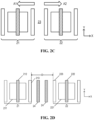
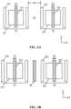
- FIG. 2A to FIG. 2D are schematic diagrams of detection of a layout according to a specific implementation of the present application.
- the layout method for an integrated circuit according to the specific implementation includes the following steps.
- step S 11 a layout is provided, the layout including a first element region 21 and a second element region 22, a spacing region 23 being provided between the first element region 21 and the second element region 22, as shown in FIG. 2A .
- the layout includes a plurality of element regions that may be arranged according to a layout requirement of the integrated circuit.
- Each element region includes a plurality of elements. Structures and arrangement manners of the elements in each element region may be the same or different, and a spacing region is provided between the adjacent element regions. The spacing region is configured to be filled with a dummy pattern to meet diffraction requirements during subsequent photolithography of the element region.
- the element may be, but is not limited to, a transistor.
- step S 12 it is detected whether a width D of the spacing region 23 is less than a preset width, and if yes, at least one of the first element region 21, the second element region 22 and the spacing region 23 is marked, and the preset width is a minimum width meeting a requirement, wherein the requirement is to fill the spacing region 23 with at least one dummy pattern 24, as shown in FIG. 2D .
- the dummy pattern refers to a pattern during photolithography that can not only compensate for the etch accuracy of the element within the element region, but also conform to DRC (Design Rule Verification).
- the preset width refers to a minimum width meeting the requirement of filling the spacing region with at least one dummy pattern, so that the etch accuracy of the element within the element region is improved.
- a space between the first element region 21 and the second element region 22 adjacent to each other is filled with the dummy pattern 24, which can help the elements within the first element region 21 and/or the second element region 22 better form diffraction in the photolithography, thereby improving the etch accuracy.
- the width D of the spacing region 23 between the first element region 21 and the second element region 22 adjacent to each other in the layout can be automatically detected and marks are made in the layout according to a detection result, so that a layout engineer can quickly and accurately position an unreasonably designed region in the layout, so as to adjust the layout in time and improve a development cycle of the layout.
- Those skilled in the art can set a specific marking manner according to an actual requirement.
- the first element region 21 and the second element region 22 that are unreasonably designed are simultaneously marked with a dashed box as shown in FIG. 2B .
- Those skilled in the art can also make marks with other patterns, colors or text.
- the first element region 21 includes a first active area 211, a first gate pattern 212 located in the first active area 211 and a first auxiliary pattern 213 located on one side of the first element region 21 toward the second element region 22, and the second element region 22 includes a second active area 221, a second gate pattern 222 located in the second active area 221 and a second auxiliary pattern 223 located on one side of the second element region 22 toward the first element region 21; and the step of detecting whether a width D of the spacing region 23 is less than a preset width specifically includes:
- the first element region 21 includes the first active area 211, and two outer sides of the first active area 211 along an X-axis direction are provided with one first auxiliary pattern 213 respectively.
- the first gate pattern 212 and the first auxiliary pattern 213 extend along a Y-axis direction perpendicular to the X-axis direction, and the first gate pattern 212 and the first auxiliary pattern 213 are arranged along the X-axis direction.
- the first gate pattern 212 may be in ashape (including a line width and a length along the Y-axis direction) the same as the first auxiliary pattern 213.
- the first auxiliary pattern 213 is configured to help better diffraction formation during the photolithography of the first gate pattern, so as to effectively control a line width of the first gate pattern to be formed (i.e., a width of the first gate pattern along the X-axis direction).
- the second element region 22 includes a second active area 221, and two outer sides of the second active area 221 along the X-axis direction are provided with one second auxiliary pattern 223 respectively.
- the second gate pattern 222 and the second auxiliary pattern 223 extend along the Y-axis direction perpendicular to the X-axis direction, and the second gate pattern 222 and the second auxiliary pattern 223 are arranged along the X-axis direction.
- the second gate pattern 222 may be in a shape (including a line width along the X-axis direction and a length along the Y-axis direction) the same as the second auxiliary pattern 223.
- the second auxiliary pattern 223 is configured to help better diffraction formation during the photolithography of the second gate pattern, so as to effectively control a line width of the second gate pattern to be formed (i.e., a width of the second gate pattern along the X-axis direction).
- the first auxiliary pattern 213 and the first gate pattern 212 are simultaneously designed and a distance between the first auxiliary pattern 213 and the first gate pattern 212 is determinate. Therefore, in this specific implementation, the distance between the first auxiliary pattern 213 and the second auxiliary pattern 223 may be directly measured; or the distance between the first active area 211 and the second active area 221 may be measured, and the distance between the first auxiliary pattern 213 and the second auxiliary pattern 223 is indirectly calculated.
- the preset width includes a first subpreset width and a second subpreset width
- the first subpreset width is a minimum width simultaneously meeting etch accuracy requirements of the first auxiliary pattern 213 and the dummy pattern 24, and the second subpreset width is a minimum width simultaneously meeting etch accuracy requirements of the second auxiliary pattern 223 and the dummy pattern.
- Specific values of the first subpreset width and the second subpreset width may be determined according to the etch accuracy that can be achieved by an etchtool actually used. Ranges of the first subpreset width and the second subpreset width are limited, so as to ensure that the dummy pattern 24 for filling can simultaneously meet etch requirements of the first element region 21 and the second element region 22.
- the method further includes the following step: adjusting a position of the first element region 21 and/or the second element region 22 to increase the width D of the spacing region 23 to the preset width.
- the width of the spacing region 23 may be adjusted in any one of the following three manners: translating the first element region 21 in a direction along the X-axis and away from the second element region 22; or translating the second element region 22 in a direction along the X-axis and away from the first element region 21; or simultaneously moving the first element region 21 and the second element region 22 in a direction along the X-axis and facing away from each other (as shown in FIG. 2C ), so that the spacing region 23 can be filled with at least one dummy pattern 24.
- the layout method for an integrated circuit further includes the following step: determining whether the width D of the spacing region 23 is less than the preset width, and if no, filling the spacing region 23 with at least one dummy pattern 24.
- the spacing region 23 is filled with at least one dummy pattern 24.
- An example in which the spacing region 23 can be filled with two dummy patterns 24 after the width D of the spacing region 23 is increased to the preset width is described in FIG. 2D .
- a specific number and shape of the dummy pattern 24 for filling, a distance between the dummy pattern 24 for filling and the first element region 21 as well as a distance between the dummy pattern 24 for filling and the second element region 22, and distances between adjacent dummy patterns 24 during filling of a plurality of dummy patterns 24 may be set by those skilled in the art according to an actual requirement, for example, according to a line width of the first gate pattern 212, a line width of the second gate pattern 222, and the like.
- the step of filling the spacing region 23 with at least one dummy pattern 24 specifically includes: determining whether a line width W1 of the first gate pattern 212 is equal to a line width W2 of the second gate pattern 222, and if yes, filling the spacing region 23 with the at least one dummy pattern 24, a line width of the dummy pattern 24 being equal to the line width of the first gate pattern 212 or the line width of the second gate pattern 222.
- the line width W1 of the first gate pattern 212 and the line width W2 of the second gate pattern 222 are equal (i.e., the first auxiliary pattern 213 and the second auxiliary pattern 223 are in a same shape) and are both less than a preset size.
- the width D of the spacing region 23 is greater than or equal to the preset width, the spacing region 23 may be filled with one or more dummy patterns 24.
- An example of filling of one dummy pattern 24 is described in FIG. 3B . In this case, the shape and size of the dummy pattern 24 for filling are the same as those of the first gate pattern 212 or the second gate pattern 222.
- a distance between the dummy pattern 24 for filling and the first auxiliary pattern 213 and a distance between the dummy pattern 24 for filling and the second auxiliary pattern 223 are equal.
- the preset size is 10 nm.
- the line width W1 of the first gate pattern 212 and the line width W2 of the second gate pattern 222 may be 5 nm, 6 nm or 7 nm.
- the step of filling the spacing region 23 with the at least one dummy pattern 24 specifically includes: determining whether a line width of the first gate pattern 212 is equal to that of the second gate pattern 222, if no, determining whether the width of the spacing region 23 meets a requirement of simultaneous filling of a first dummy pattern 241 and a second dummy pattern 242, and if yes, simultaneously filling the spacing region 23 with the first dummy pattern 241 and the second dummy pattern 242, the first dummy pattern 241 being a pattern with a line width the same as the first gate pattern 212, and the second dummy pattern 242 being a pattern with a line width the same as the second gate pattern 222.
- Whether the width of the spacing region 23 meets a requirement of simultaneous filling of a first dummy pattern 241 and a second dummy pattern 242 specifically includes: a distance between the first dummy pattern 241 filling the spacing region 23 and the first auxiliary pattern 213 being greater than or equal to the first subpreset width, and a distance between the second dummy pattern 242 filling the spacing region 23 and the second auxiliary pattern 223 being greater than or equal to the second subpreset width.
- the line width W1 of the first gate pattern 212 and the line width W2 of the second gate pattern 222 are less than the preset size
- the line width W1 of the first gate pattern 212 is less than the line width W2 of the second gate pattern 222 (i.e., the line width of the first auxiliary pattern 213 is less than that of the second auxiliary pattern 223)
- the width of the spacing region 23 meets the requirement of simultaneous filling of the first dummy pattern 241 and the second dummy pattern 242; then, the spacing region 23 may be simultaneously filled with two first dummy patterns 241 and two second dummy patterns 242, as shown in FIG. 3D .
- the first dummy pattern 241 is located on one side of the spacing region 23 close to the first auxiliary pattern 213, and a line width of the first dummy pattern 241 is equal to that of the first gate pattern 212; the second dummy pattern 242 is located on one side of the spacing region 23 close to the second auxiliary pattern 223, and a line width of the second dummy pattern 242 is equal to that of the second gate pattern 222.
- the reason why the spacing region 23 is filled with the two first dummy patterns 241 is that at least three patterns in a same shape (the first auxiliary pattern 213 and the first dummy pattern 241) are arranged on one side of the first gate pattern 212 to better improve a diffraction effect of the first gate pattern 212 during photolithography.
- the reason why the spacing region 23 is filled with the two second dummy patterns 242 is that at least three patterns in a same shape (the second auxiliary pattern 223 and the second dummy pattern 242) are arranged on one side of the second gate pattern 222 to better improve a diffraction effect of the second gate pattern 222 during photolithography.
- a length of the first dummy pattern 241 for filling (a length along the Y-axis direction in FIG. 3C ) is equal to a length of the first auxiliary pattern 213 (a length along the Y-axis direction in FIG. 3C ); and a length of the second dummy pattern 242 for filling (a length along the Y-axis direction in FIG. 3C ) is equal to a length of the second auxiliary pattern 223 (a length along the Y-axis direction in FIG. 3C ).
- a distance between the first dummy pattern 241 and the second dummy pattern 242 adjacent to each other and filling the spacing region 23 is greater than or equal to a first threshold.
- a specific value of the first threshold may be set according to process capability and an actual manufacturing condition, such as a photolithography accuracy requirement.
- the method further includes the following step: determining whether a distance between the first dummy pattern 241 and the second dummy pattern 242 after filling is less than a first threshold, and if yes, enabling the first dummy pattern 241 for fillingto be connected to the second dummy pattern 242for filling.
- the step of filling the spacing region 23 with at least one dummy pattern 24 specifically includes: determining whether a line width of the first gate pattern 212 is equal to that of the second gate pattern 222, if no, determining whether the width of the spacing region 23 meets a requirement of simultaneous filling of a first dummy pattern 241 and a second dummy pattern 242, if no, re-determining whether the line width of the first gate pattern 212 is less than that of the second gate pattern 222, if yes, filling the spacing region 23 with only the first dummy pattern 241, and if no, filling the spacing region 23 with only the second dummy pattern 242, the first dummy pattern 241 being a pattern with a line width the same as the first gate pattern 212, and the second dummy pattern 242 being a pattern with a line width the same as the second gate pattern 222.
- a length of the first dummy pattern 241 is equal to that of the first auxiliary pattern 213, and a length of the second dummy pattern 242 is equal to that of the second auxiliary pattern 223.
- the layout method for an integrated circuit further includes the following step: determining whether a distance between the first dummy pattern 241 after filling and the second auxiliary pattern 223 is less than a first threshold, and if yes, enabling the first dummy pattern 241 for filling to be connected to the second auxiliary pattern 223.
- the line width W1 of the first gate pattern 212 is less than the preset size, and the line width W2 of the second gate pattern 222 is greater than the preset size; that is, the line width W1 of the first gate pattern 212 is not equal to the line width W2 of the second gate pattern 222.
- the spacing region may be filled with only one first dummy pattern 241 having a line width the same as the first gate pattern 212 or the first auxiliary pattern 213, as shown in FIG. 3F .
- the spacing region 23 may be filled with only the second dummy pattern 242.
- a specific value of the first threshold may be set according to process capability and an actual manufacturing condition, such as a photolithography accuracy requirement.
- the first dummy pattern 241 for filling is enabled to be directly connected to the second auxiliary pattern 223.
- the first dummy pattern 241 for filling is enabled to be isolated from the second auxiliary pattern 223.
- the layout method for an integrated circuit further includes the following step: determining whether a conductive plug 25 adjacent to the first element region exists on a periphery of the first element region 21, and if yes, filling a space between the first element region 21 and the conductive plug 25 with a plug dummy pattern 244, a line width of the plug dummy pattern 244 being equal to that of the first gate pattern 212.
- the space between the first element region 21 and the conductive plug 25 may also be filled with at least two plug dummy patterns 244, as shown in FIG. 3H , so that one side of the first gate pattern toward the conductive plug 25 meets the requirement of having at least three patterns in a same shape (including the first auxiliary pattern and the dummy pattern for filling), so as to improve a photolithography effect.
- the line width of the plug dummy pattern 244 is equal to that of the first gate pattern 212, and the length of the dummy pattern 24 is equal to that of the first auxiliary pattern 213.
- the layout further includes a conductive plug 25 and a third element region 26 adjacent to the first element region 21; the third element region 26 includes a third active area, a third gate pattern 261 located in the third active area and a third auxiliary pattern 262 located on an outer side of the third active area; and the layout method for an integrated circuit further includes the following step: determining whether the first element region 21, the third element region 26 and the conductive plug 25 jointly define a blank region 28, and if yes, filling the blank region 28 with a third dummy pattern 243 matching both the first element region 21 and the third element region 26, the blank region 28 being a region provided with no gate pattern.
- the blank region 28 in this specific implementation is the region provided with no gate pattern.
- the third dummy pattern 243 matching both the first element region 21 and the third element region 26 means that a shape of the third dummy pattern 243 matches one or more of extension directions, extension lengths and line widths of elements in the first element region 21 and the third element region 26 and a spacing distance between adjacent elements, so as to improve the photolithography quality of the patterns in the first element region 21 and the third element region 26.
- the first gate pattern 212 and the third gate pattern 261 extend along a first direction, the first gate pattern 212 and the third gate pattern 261 are spaced along a second direction, the first direction is perpendicular to the second direction, and a length or position of the first gate pattern 212 in the first direction is beyond that of the third gate pattern 261; and the step of filling the blank region 28 with the third dummy pattern 243 matching both the first element region 21 and the third element region 26 specifically includes: filling the blank region 28 with the third dummy pattern 243 extending along the first direction, a position of the third dummy pattern 243 being aligned with that of the third gate pattern 261 or the third auxiliary pattern 262 in the first direction and aligned with that of the first gate pattern 212 or the first auxiliary pattern 213 in the second direction.
- the first direction is a Y-axis direction
- the second direction is an X-axis direction.
- the blank region 28 is filled with a plurality of third dummy patterns 243 extending along the Y-axis direction and arranged along the X-axis direction. A boundary of each of the dummy patterns close to one side of the conductive plug 25 is flush with the first gate pattern 212.
- the plurality of third dummy patterns 243 are aligned with a plurality of third gate patterns 261 in the third element region 26 and the third auxiliary pattern 262 located outside the third active area.
- the blank region 28 is filled with the plurality of third dummy patterns 243; and in the second direction, a distance between adjacent third dummy patterns 243 is equal to that between the third gate pattern 261 and the third auxiliary pattern 262.
- the blank region 28 may be filled with a plurality of third dummy patterns 243 completely.
- a number of the third dummy pattern 243 filling the blank region 28 is equal to a sum of numbers of the third gate pattern 261 and the third auxiliary pattern 262 in the third element region 26, and the distance between adjacent third dummy patterns 243 is equal to that between the third gate pattern 261 and the third auxiliary pattern 262.
- the layout method for an integrated circuit further includes the following step: determining whether another element pattern exists in the blank region 28, and if yes, controlling a minimum distance between the third dummy pattern 243 and the another element pattern to be greater than or equal to a second threshold.
- the third dummy pattern 243 is set to avoid the metal connection structure 263, as shown in FIG. 3J .
- the layout further includes a fourth element region 27 and the first element region 21, the third element region 26, the fourth element region 27 and the conductive plug 25 jointly define a blank region, the third dummy pattern for filling should be further aligned with a fourth gate pattern and a fourth auxiliary pattern in the fourth element region.
- a specific value of the second threshold may be set according to process capability and an actual manufacturing condition, such as a photolithography accuracy requirement.
- the first threshold may be equal or not equal to the second threshold, which may be set by those skilled in the art according to an actual manufacturing requirement.
- the method further includes the following step: determining whether the width of the spacing region 23 is less than the first subpreset width, and if no, filling the spacing region 23 with the first dummy pattern 241, a line width of the first dummy pattern 241 being equal to that of the first gate pattern 212.
- the method further includes the following step: determining whether a distance between the first dummy pattern 241 filling the spacing region 23 and the second auxiliary pattern 213 is less than a first threshold, and if yes, enabling the first dummy pattern 241 for filling to be connected to the second auxiliary pattern 223.
- the method may further include the following step: determining whether the width of the spacing region 23 is less than the first subpreset width, and if no, filling the spacing region 23 with the first dummy pattern 241, the first dummy pattern 241 being a pattern with a line width the same as that of the first gate pattern 212.
- the method may further include the following step: determining whether the width of the spacing region 23 is less than the second subpreset width, and if no, filling the spacing region 23 with the second dummy pattern 242, the second dummy pattern 242 being a pattern with a line width the same as that of the second gate pattern 222. That is, a corresponding determination manner can be selected according to relative sizes of the first subpreset width and the second subpreset width.
- the width of the spacing region 23 is determined to be less than the preset width and greater than the first subpreset width, it is determined whether a distance between the first dummy pattern 241 filling the spacing region 23 and the second auxiliary pattern 213 is less than the first threshold, and if yes, the first dummy pattern 241 for filling is enabled to be connected to the second auxiliary pattern 223.
- FIG. 4 is a structural block diagram of a layout apparatus for an integrated circuit according to a specific implementation of the present application.
- the layout apparatus for an integrated circuit according to this specific implementation may lay out a layout by using the layout method for an integrated circuit shown in FIG. 1 , FIG. 2A to FIG. 2D and FIG. 3A to FIG. 3J .
- the layout apparatus for an integrated circuit according to the specific implementation includes:
- a memory module 40 configured to store a layout, the layout including a first element region 21 and a second element region 22, a spacing region 23 being provided between the first element region 21 and the second element region 22, wherein the memory module 40 may include any combination of different types of non-volatile memory apparatuses and/or volatile memory apparatuses, and the volatile memory apparatus (such as a memory apparatus) may be (but not limited to) a random access memory (RAM), such as a dynamic random access memory (DRAM) or a synchronous dynamic random access memory (SDRAM); and a detection module 41 connected to the memory module 40 and configured to detect whether a width of the spacing region 23 is less than a preset width, and if yes, mark at least one of the first element region 21, the second element region 22 and the spacing region 23, the preset width being a minimum width meeting a requirement, wherein the requirement is to fill the spacing region 23with at least one dummy pattern 24.
- RAM random access memory
- DRAM dynamic random access memory
- SDRAM synchronous dynamic random access memory
- the detection module 41 may be a microcontroller, a dedicated logic circuit system (for example, a field-programmable gate array (FPGA), a dedicated integrated circuit (ASIC), or the like), or other suitable processors.
- a microcontroller data in the memory module 40 may be read, it is detected whether a width of the spacing region 23 is less than a preset width, and if yes, at least one of the first element region 21, the second element region 22 and the spacing region 23 is marked.
- the first element region 21 includes a first active area 211, a first gate pattern 212 located in the first active area 211 and a first auxiliary pattern 213 located on one side of the first element region 211 toward the second element region 22, and the second element region 22 includes a second active area 221, a second gate pattern 222 located in the second active area 221 and a second auxiliary pattern 223 located on one side of the second active area 221 toward the first element region 21; and
- the layout apparatus for an integrated circuit further includes: a filling module 42 connected to the detection module 41 and configured to fill the spacing region 23 with at least one dummy pattern 24 when the detection module 41 detects that the width of the spacing region 23 is greater than the preset width.
- the filling module 42 may be implemented in at least one hardware form of Digital Signal Processing (DSP), a Field-Programmable Gate Array (FPGA) and a Programmable Logic Array (PLA).
- DSP Digital Signal Processing
- FPGA Field-Programmable Gate Array
- PDA Programmable Logic Array
- the field-programmable gate array may be arranged as a graphics processing unit (GPU) configured to execute a special-purpose instruction, such as a graph fill instruction.
- the graphics processing unit (GPU) instructs the filling module 42 to fill the spacing region 23 with the at least one dummy pattern 24.
- the filling module 42 is further configured to determine whether a line width W1 of the first gate pattern 212 is equal to a line width W2 of the second gate pattern 222, and if yes, fill the spacing region 23 with the at least one dummy pattern 24, a line width of the dummy pattern 24 being equal to the line width of the first gate pattern 212 or the line width of the second gate pattern 222.
- the filling module 42 is further configured to determine whether a line width of the first gate pattern 212 is equal to that of the second gate pattern 222, if no, determine whether the width of the spacing region 23 meets a requirement of simultaneous filling of a first dummy pattern 241 and a second dummy pattern 242, and if yes, simultaneously fill the spacing region 23 with the first dummy pattern 241 and the second dummy pattern 242, the first dummy pattern 241 being a pattern with a line width the same as the first gate pattern 212, and the second dummy pattern 242 being a pattern with a line width the same as the second gate pattern 222.
- the filling module 42 is further configured to determine whether a line width of the first gate pattern 212 is equal to that of the second gate pattern 222, if no, determine whether the width of the spacing region 23 meets a requirement of simultaneous filling of a first dummy pattern 241 and a second dummy pattern 242, if no, re-determine whether the line width of the first gate pattern 212 is less than that of the second gate pattern 222, if yes, fill the spacing region 23 with only the first dummy pattern 241, and if no, fill the spacing region 23 with only the second dummy pattern 242, the first dummy pattern 241 being a pattern with a line width the same as the first gate pattern 212, and the second dummy pattern 242 being a pattern with a line width the same as the second gate pattern 222.
- the filling module 42 is further configured to determine whether a conductive plug 25 adjacent to the first element region exists on a periphery of the first element region 21, and if yes, fill a space between the first element region 21 and the conductive plug 25 with a plug dummy pattern 244, a line width of the plug dummy pattern 244 being equal to that of the first gate pattern 212.
- the layout further includes a conductive plug 25 and a third element region 26 adjacent to the first element region 21;
- the third element region includes a third active area, a third gate pattern 261 located in the third active area and a third auxiliary pattern 262 located on an outer side of the third active area;
- the filling module 42 is further configured to determine whether the first element region 21, the third element region 26 and the conductive plug 25 jointly define a blank region 28, and if yes, fill the blank region 28 with the third dummy pattern 243 matching both the first element region 21 and the third element region 26, the blank region 28 being a region provided with no gate pattern.
- the detection module 41 is further configured to, after at least one of the first element region 21, the second element region 22 and the spacing region 23 is marked, adjust positions of the first element region 21 and/or the second element region 22 to increase the width of the spacing region 23 to the preset width.
- a width of a spacing region between two adjacent element regions in a layout is automatically detected, and an element region and/or a spacing region not meeting a filling requirement of a dummy pattern are/is marked, so as to quickly and accurately position a poorly-placed element region in the layout, so that the layout can be adjusted in time, which saves human resources, improves the layout efficiency and layout precision of the integrated circuit, and lays a foundation for improving photolithography quality, shortening a development cycle of the integrated circuit, improving a yield of semiconductor products and the like.
Landscapes
- Engineering & Computer Science (AREA)
- Computer Hardware Design (AREA)
- Physics & Mathematics (AREA)
- Theoretical Computer Science (AREA)
- General Engineering & Computer Science (AREA)
- Evolutionary Computation (AREA)
- Geometry (AREA)
- General Physics & Mathematics (AREA)
- Architecture (AREA)
- Manufacturing & Machinery (AREA)
- Design And Manufacture Of Integrated Circuits (AREA)
- Semiconductor Integrated Circuits (AREA)
Abstract
Description
- This application claims priority to
Chinese Patent Application No. 202011237506.6 filed on November 9, 2020 - The present application relates to the field of integrated circuit manufacturing, and in particular, to a layout method and a layout apparatus for an integrated circuit.
- A Dynamic Random Access Memory (DRAM) is a semiconductor device commonly used in electronic devices such as computers, and consists of a plurality of repeating memory cells. Each memory cell generally includes a transistor and a capacitor. The transistor has a gate electrically connected to a wordline, a source electrically connected to a bitline and a drain electrically connected to the capacitor. A wordline voltage on the wordline can control ON and OFF of the transistor so that through the bitline, data information stored in the capacitor can be read or data information is written to the capacitor.
- With the continuous reduction of DRAM process nodes, requirements for uniformity of a layout are becoming ever higher. In a latest LP (Low Power) process, a process library has three small trench lengths (5X m, 6X nm, and 7X nm). The smaller size makes a single-node process of the DRAM more complex, and an etch error is very easy to occur in a manufacturing process. In order to compensate for this error, pseudo-gates with a corresponding length and spaced by a specific distance may generally be added to two sides of the transistor to facilitate the formation of diffraction during photolithography, so as to improve the etch accuracy of the trench length of the transistor in an edge region. However, since a number of transistors on the layout is tens of millions and the placement of transistors with small trench lengths is extremely complex, a tight development cycle makes engineers unable to manually add the pseudo-gates in a short time, which limits the improvement of subsequent chip photolithography quality.
- Therefore, how to improve the layout efficiency and layout precision of an integrated circuit, improve photolithography quality, shorten a development cycle of the integrated circuit, and improve a yield of semiconductor products are an urgent technical problem to be solved currently.
- Embodiments of the present application provide a layout method and a layout apparatus for an integrated circuit, which solves the problem of low efficiency of an existing integrated circuit layout to some extent, so as to improve the layout precision, improve the photolithography quality, shorten the development cycle of the integrated circuit, and improve the yield of semiconductor products.
- According to one aspect of the embodiments of the present application, a layout method for an integrated circuit is provided, including the following steps:
- providing a layout, the layout including a first element region and a second element region, a spacing region being provided between the first element region and the second element region; and
- detecting whether a width of the spacing region is less than a preset width, and if yes, marking at least one of the first element region, the second element region and the spacing region, the preset width being a minimum width meeting a requirement, wherein the requirement is to fill the spacing region with at least one dummy pattern.
- According to another aspect of the embodiments of the present application, a layout apparatus for an integrated circuit is provided, including:
- a memory module configured to store a layout, the layout including a first element region and a second element region, a spacing region being provided between the first element region and the second element region; and
- a detection module connected to the memory module and configured to detect whether a width of the spacing region is less than a preset width, and if yes, mark at least one of the first element region, the second element region and the spacing region, the preset width being a minimum width meeting a requirement, wherein the requirement is to fill the spacing region with at least one dummy pattern.
- Through the layout method and the layout apparatus for an integrated circuit according to the embodiments of the present application, a width of a spacing region between two adjacent element regions in a layout is automatically detected, and an element region and/or a spacing region not meeting a filling requirement of a dummy pattern are/is marked, so as to quickly and accurately position a poorly-placed element region in the layout, so that the layout can be adjusted in time, which saves human resources, improves the layout efficiency and layout precision of the integrated circuit, and lays a foundation for improving the photolithography quality, shortening the development cycle of the integrated circuit, and improving the yield of semiconductor products and the like.
- The above and other objectives, features and advantages of the present application will become more apparent from following descriptions of the embodiments of the present application with reference to accompanying drawings, in which:
-
FIG. 1 is a flowchart of a layout method for an integrated circuit according to a specific implementation of the present application; -
FIG. 2A to FIG. 2D are schematic diagrams of detection of a layout according to a specific implementation of the present application; -
FIG. 3A to FIG. 3J are schematic diagrams of filling of layouts under different scenarios with dummy patterns according to a specific implementation of the present application; and -
FIG. 4 is a structural block diagram of a layout apparatus for an integrated circuit according to a specific implementation of the present application. - In order to make the objectives, technical solutions and advantages of the present application clearer, the present application is described in further detail below through embodiments in conjunction with the accompanying drawings. However, it is to be understood that these descriptions are illustrative only and not intended to limit the scope of the present application. Further, in the following, descriptions of known structures and technologies are omitted to avoid unnecessary confusion between concepts of the present application.
- In the drawings, various structural diagrams and cross-sectional views of a semiconductor device according to the present application are shown. The drawings are not drawn to scale, and some details may be enlarged while some details may be omitted for sake of clarity. Shapes, relative sizes and position relationships of regions and layers shown in the drawings are only illustrative, and deviations therefrom may occur due to manufacture tolerances and technique limitations in practice. Those skilled in the art can also design regions/layers of other different shapes, sizes, and relative positions according to an actual requirement.
- This specific implementation provides a layout method for an integrated circuit.
FIG. 1 is a flowchart of a layout method for an integrated circuit according to a specific implementation of the present application, andFIG. 2A to FIG. 2D are schematic diagrams of detection of a layout according to a specific implementation of the present application. As shown inFIG. 1 and FIG. 2A toFIG. 2D , the layout method for an integrated circuit according to the specific implementation includes the following steps. - In step S 11, a layout is provided, the layout including a
first element region 21 and asecond element region 22, aspacing region 23 being provided between thefirst element region 21 and thesecond element region 22, as shown inFIG. 2A . - Specifically, the layout includes a plurality of element regions that may be arranged according to a layout requirement of the integrated circuit. Each element region includes a plurality of elements. Structures and arrangement manners of the elements in each element region may be the same or different, and a spacing region is provided between the adjacent element regions. The spacing region is configured to be filled with a dummy pattern to meet diffraction requirements during subsequent photolithography of the element region. The element may be, but is not limited to, a transistor.
- In
step S 12, it is detected whether a width D of thespacing region 23 is less than a preset width, and if yes, at least one of thefirst element region 21, thesecond element region 22 and thespacing region 23 is marked, and the preset width is a minimum width meeting a requirement, wherein the requirement is to fill thespacing region 23 with at least onedummy pattern 24, as shown inFIG. 2D . - Specifically, the dummy pattern refers to a pattern during photolithography that can not only compensate for the etch accuracy of the element within the element region, but also conform to DRC (Design Rule Verification). The preset width refers to a minimum width meeting the requirement of filling the spacing region with at least one dummy pattern, so that the etch accuracy of the element within the element region is improved. During the photolithography, a space between the
first element region 21 and thesecond element region 22 adjacent to each other is filled with thedummy pattern 24, which can help the elements within thefirst element region 21 and/or thesecond element region 22 better form diffraction in the photolithography, thereby improving the etch accuracy. However, if the width D of thespacing region 23 is over narrow, the filling of thedummy pattern 24 is impossible due to the limitation of photolithography diffraction, thereby affecting the implementation of subsequent photolithography. In this specific implementation, the width D of thespacing region 23 between thefirst element region 21 and thesecond element region 22 adjacent to each other in the layout can be automatically detected and marks are made in the layout according to a detection result, so that a layout engineer can quickly and accurately position an unreasonably designed region in the layout, so as to adjust the layout in time and improve a development cycle of the layout. Those skilled in the art can set a specific marking manner according to an actual requirement. In this specific implementation, thefirst element region 21 and thesecond element region 22 that are unreasonably designed are simultaneously marked with a dashed box as shown inFIG. 2B . Those skilled in the art can also make marks with other patterns, colors or text. - Optionally, the
first element region 21 includes a firstactive area 211, afirst gate pattern 212 located in the firstactive area 211 and a firstauxiliary pattern 213 located on one side of thefirst element region 21 toward thesecond element region 22, and thesecond element region 22 includes a secondactive area 221, asecond gate pattern 222 located in the secondactive area 221 and a secondauxiliary pattern 223 located on one side of thesecond element region 22 toward thefirst element region 21; and the step of detecting whether a width D of thespacing region 23 is less than a preset width specifically includes: - measuring a distance between the first
auxiliary pattern 213 and the secondauxiliary pattern 223; or - measuring a distance between the first
active area 211 and the secondactive area 221, and calculating a distance between the firstauxiliary pattern 213 and the secondauxiliary pattern 223. - Specifically, the
first element region 21 includes the firstactive area 211, and two outer sides of the firstactive area 211 along an X-axis direction are provided with one firstauxiliary pattern 213 respectively. Thefirst gate pattern 212 and the firstauxiliary pattern 213 extend along a Y-axis direction perpendicular to the X-axis direction, and thefirst gate pattern 212 and the firstauxiliary pattern 213 are arranged along the X-axis direction. Thefirst gate pattern 212 may be in ashape (including a line width and a length along the Y-axis direction) the same as the firstauxiliary pattern 213. The firstauxiliary pattern 213 is configured to help better diffraction formation during the photolithography of the first gate pattern, so as to effectively control a line width of the first gate pattern to be formed (i.e., a width of the first gate pattern along the X-axis direction). Thesecond element region 22 includes a secondactive area 221, and two outer sides of the secondactive area 221 along the X-axis direction are provided with one secondauxiliary pattern 223 respectively. Thesecond gate pattern 222 and the secondauxiliary pattern 223 extend along the Y-axis direction perpendicular to the X-axis direction, and thesecond gate pattern 222 and the secondauxiliary pattern 223 are arranged along the X-axis direction. Thesecond gate pattern 222 may be in a shape (including a line width along the X-axis direction and a length along the Y-axis direction) the same as the secondauxiliary pattern 223. The secondauxiliary pattern 223 is configured to help better diffraction formation during the photolithography of the second gate pattern, so as to effectively control a line width of the second gate pattern to be formed (i.e., a width of the second gate pattern along the X-axis direction). - During the layout design, generally, the first
auxiliary pattern 213 and thefirst gate pattern 212 are simultaneously designed and a distance between the firstauxiliary pattern 213 and thefirst gate pattern 212 is determinate. Therefore, in this specific implementation, the distance between the firstauxiliary pattern 213 and the secondauxiliary pattern 223 may be directly measured; or the distance between the firstactive area 211 and the secondactive area 221 may be measured, and the distance between the firstauxiliary pattern 213 and the secondauxiliary pattern 223 is indirectly calculated. - Optionally, the preset width includes a first subpreset width and a second subpreset width;
- the first subpreset width is a minimum width meeting the requirement and existing between the
dummy pattern 24 for filling and the firstauxiliary pattern 213, and the second subpreset width is a minimum width meeting the requirement and existing between thedummy pattern 24 for filling and the secondauxiliary pattern 223; and - the minimum width meeting the requirement and existing between the
dummy pattern 24 for filling and the firstauxiliary pattern 213 is equal to a distance between the firstauxiliary pattern 213 and thefirst gate pattern 212, and the minimum width meeting the requirement and existing between thedummy pattern 24 for filling and the secondauxiliary pattern 223 is equal to a distance between the secondauxiliary pattern 223 and thesecond gate pattern 222. - Specifically, the first subpreset width is a minimum width simultaneously meeting etch accuracy requirements of the first
auxiliary pattern 213 and thedummy pattern 24, and the second subpreset width is a minimum width simultaneously meeting etch accuracy requirements of the secondauxiliary pattern 223 and the dummy pattern. Specific values of the first subpreset width and the second subpreset width may be determined according to the etch accuracy that can be achieved by an etchtool actually used. Ranges of the first subpreset width and the second subpreset width are limited, so as to ensure that thedummy pattern 24 for filling can simultaneously meet etch requirements of thefirst element region 21 and thesecond element region 22. - Optionally, after the step of marking at least one of the
first element region 21, thesecond element region 22 and thespacing region 23, the method further includes the following step:
adjusting a position of thefirst element region 21 and/or thesecond element region 22 to increase the width D of thespacing region 23 to the preset width. - Specifically, after an unreasonably designed position in the layout is positioned, the width of the
spacing region 23 may be adjusted in any one of the following three manners: translating thefirst element region 21 in a direction along the X-axis and away from thesecond element region 22; or translating thesecond element region 22 in a direction along the X-axis and away from thefirst element region 21; or simultaneously moving thefirst element region 21 and thesecond element region 22 in a direction along the X-axis and facing away from each other (as shown inFIG. 2C ), so that thespacing region 23 can be filled with at least onedummy pattern 24. - Optionally, the layout method for an integrated circuit further includes the following step:
determining whether the width D of thespacing region 23 is less than the preset width, and if no, filling thespacing region 23 with at least onedummy pattern 24. - Specifically, when it is detected that the width of the
spacing region 23 is greater than the preset width, thespacing region 23 is filled with at least onedummy pattern 24. An example in which thespacing region 23 can be filled with twodummy patterns 24 after the width D of thespacing region 23 is increased to the preset width is described inFIG. 2D . A specific number and shape of thedummy pattern 24 for filling, a distance between thedummy pattern 24 for filling and thefirst element region 21 as well as a distance between thedummy pattern 24 for filling and thesecond element region 22, and distances betweenadjacent dummy patterns 24 during filling of a plurality ofdummy patterns 24 may be set by those skilled in the art according to an actual requirement, for example, according to a line width of thefirst gate pattern 212, a line width of thesecond gate pattern 222, and the like. - Optionally, the step of filling the
spacing region 23 with at least onedummy pattern 24 specifically includes:
determining whether a line width W1 of thefirst gate pattern 212 is equal to a line width W2 of thesecond gate pattern 222, and if yes, filling thespacing region 23 with the at least onedummy pattern 24, a line width of thedummy pattern 24 being equal to the line width of thefirst gate pattern 212 or the line width of thesecond gate pattern 222. - For example, as shown in
FIG. 3A , the line width W1 of thefirst gate pattern 212 and the line width W2 of thesecond gate pattern 222 are equal (i.e., the firstauxiliary pattern 213 and the secondauxiliary pattern 223 are in a same shape) and are both less than a preset size. When the width D of thespacing region 23 is greater than or equal to the preset width, thespacing region 23 may be filled with one ormore dummy patterns 24. An example of filling of onedummy pattern 24 is described inFIG. 3B . In this case, the shape and size of thedummy pattern 24 for filling are the same as those of thefirst gate pattern 212 or thesecond gate pattern 222. A distance between thedummy pattern 24 for filling and the firstauxiliary pattern 213 and a distance between thedummy pattern 24 for filling and the secondauxiliary pattern 223 are equal. In this specific implementation, the preset size is 10 nm. For example, the line width W1 of thefirst gate pattern 212 and the line width W2 of thesecond gate pattern 222 may be 5 nm, 6 nm or 7 nm. - Optionally, the step of filling the
spacing region 23 with the at least onedummy pattern 24 specifically includes:
determining whether a line width of thefirst gate pattern 212 is equal to that of thesecond gate pattern 222, if no, determining whether the width of thespacing region 23 meets a requirement of simultaneous filling of afirst dummy pattern 241 and asecond dummy pattern 242, and if yes, simultaneously filling thespacing region 23 with thefirst dummy pattern 241 and thesecond dummy pattern 242, thefirst dummy pattern 241 being a pattern with a line width the same as thefirst gate pattern 212, and thesecond dummy pattern 242 being a pattern with a line width the same as thesecond gate pattern 222. - Whether the width of the
spacing region 23 meets a requirement of simultaneous filling of afirst dummy pattern 241 and asecond dummy pattern 242 specifically includes: a distance between thefirst dummy pattern 241 filling thespacing region 23 and the firstauxiliary pattern 213 being greater than or equal to the first subpreset width, and a distance between thesecond dummy pattern 242 filling thespacing region 23 and the secondauxiliary pattern 223 being greater than or equal to the second subpreset width. - For example, as shown in
FIG. 3C , the line width W1 of thefirst gate pattern 212 and the line width W2 of thesecond gate pattern 222 are less than the preset size, the line width W1 of thefirst gate pattern 212 is less than the line width W2 of the second gate pattern 222 (i.e., the line width of the firstauxiliary pattern 213 is less than that of the second auxiliary pattern 223), and the width of thespacing region 23 meets the requirement of simultaneous filling of thefirst dummy pattern 241 and thesecond dummy pattern 242; then, thespacing region 23 may be simultaneously filled with twofirst dummy patterns 241 and twosecond dummy patterns 242, as shown inFIG. 3D . Thefirst dummy pattern 241 is located on one side of thespacing region 23 close to the firstauxiliary pattern 213, and a line width of thefirst dummy pattern 241 is equal to that of thefirst gate pattern 212; thesecond dummy pattern 242 is located on one side of thespacing region 23 close to the secondauxiliary pattern 223, and a line width of thesecond dummy pattern 242 is equal to that of thesecond gate pattern 222. In this specific implementation, the reason why thespacing region 23 is filled with the twofirst dummy patterns 241 is that at least three patterns in a same shape (the firstauxiliary pattern 213 and the first dummy pattern 241) are arranged on one side of thefirst gate pattern 212 to better improve a diffraction effect of thefirst gate pattern 212 during photolithography. The reason why thespacing region 23 is filled with the twosecond dummy patterns 242 is that at least three patterns in a same shape (the secondauxiliary pattern 223 and the second dummy pattern 242) are arranged on one side of thesecond gate pattern 222 to better improve a diffraction effect of thesecond gate pattern 222 during photolithography. - In order to further improve the etch diffraction effect, a length of the
first dummy pattern 241 for filling (a length along the Y-axis direction inFIG. 3C ) is equal to a length of the first auxiliary pattern 213 (a length along the Y-axis direction inFIG. 3C ); and a length of thesecond dummy pattern 242 for filling (a length along the Y-axis direction inFIG. 3C ) is equal to a length of the second auxiliary pattern 223 (a length along the Y-axis direction inFIG. 3C ). - In this specific implementation, optionally, a distance between the
first dummy pattern 241 and thesecond dummy pattern 242 adjacent to each other and filling thespacing region 23 is greater than or equal to a first threshold. A specific value of the first threshold may be set according to process capability and an actual manufacturing condition, such as a photolithography accuracy requirement. In other specific implementations, the method further includes the following step:
determining whether a distance between thefirst dummy pattern 241 and thesecond dummy pattern 242 after filling is less than a first threshold, and if yes, enabling thefirst dummy pattern 241 for fillingto be connected to the second dummy pattern 242for filling. - Optionally, the step of filling the
spacing region 23 with at least onedummy pattern 24 specifically includes:
determining whether a line width of thefirst gate pattern 212 is equal to that of thesecond gate pattern 222, if no, determining whether the width of thespacing region 23 meets a requirement of simultaneous filling of afirst dummy pattern 241 and asecond dummy pattern 242, if no, re-determining whether the line width of thefirst gate pattern 212 is less than that of thesecond gate pattern 222, if yes, filling thespacing region 23 with only thefirst dummy pattern 241, and if no, filling thespacing region 23 with only thesecond dummy pattern 242, thefirst dummy pattern 241 being a pattern with a line width the same as thefirst gate pattern 212, and thesecond dummy pattern 242 being a pattern with a line width the same as thesecond gate pattern 222. - Optionally, a length of the
first dummy pattern 241 is equal to that of the firstauxiliary pattern 213, and a length of thesecond dummy pattern 242 is equal to that of the secondauxiliary pattern 223. - Optionally, the layout method for an integrated circuit further includes the following step:
determining whether a distance between thefirst dummy pattern 241 after filling and the secondauxiliary pattern 223 is less than a first threshold, and if yes, enabling thefirst dummy pattern 241 for filling to be connected to the secondauxiliary pattern 223. - For example, as shown in
FIG. 3E , the line width W1 of thefirst gate pattern 212 is less than the preset size, and the line width W2 of thesecond gate pattern 222 is greater than the preset size; that is, the line width W1 of thefirst gate pattern 212 is not equal to the line width W2 of thesecond gate pattern 222. If the width D of thespacing region 23 is insufficient for the filling of two dummy patterns and the line width W1 of thefirst gate pattern 212 is less than the line width W2 of thesecond gate pattern 222, the spacing region may be filled with only onefirst dummy pattern 241 having a line width the same as thefirst gate pattern 212 or the firstauxiliary pattern 213, as shown inFIG. 3F . This is because the larger the line width, the less affected by the diffraction effect during the photolithography. Due to the smaller line width of thefirst dummy pattern 241, the photolithography of thesecond gate pattern 222 is less affected. Conversely, if the line width W1 of thefirst gate pattern 212 is greater than the line width W2 of thesecond gate pattern 222, thespacing region 23 may be filled with only thesecond dummy pattern 242. - A specific value of the first threshold may be set according to process capability and an actual manufacturing condition, such as a photolithography accuracy requirement. When a distance between the
first dummy pattern 241 after filling and the secondauxiliary pattern 223 is less than the first threshold, thefirst dummy pattern 241 for filling is enabled to be directly connected to the secondauxiliary pattern 223. When the distance between thefirst dummy pattern 241 after filling and the secondauxiliary pattern 223 is greater than the first threshold, thefirst dummy pattern 241 for filling is enabled to be isolated from the secondauxiliary pattern 223. - Optionally, the layout method for an integrated circuit further includes the following step:
determining whether aconductive plug 25 adjacent to the first element region exists on a periphery of thefirst element region 21, and if yes, filling a space between thefirst element region 21 and theconductive plug 25 with aplug dummy pattern 244, a line width of theplug dummy pattern 244 being equal to that of thefirst gate pattern 212. - For example, as shown in
FIG. 3G , when it is detected that theconductive plug 25 adjacent to the first element region exists on the periphery of thefirst element region 21, the space between thefirst element region 21 and theconductive plug 25 may also be filled with at least twoplug dummy patterns 244, as shown inFIG. 3H , so that one side of the first gate pattern toward theconductive plug 25 meets the requirement of having at least three patterns in a same shape (including the first auxiliary pattern and the dummy pattern for filling), so as to improve a photolithography effect. The line width of theplug dummy pattern 244 is equal to that of thefirst gate pattern 212, and the length of thedummy pattern 24 is equal to that of the firstauxiliary pattern 213. - Optionally, the layout further includes a
conductive plug 25 and athird element region 26 adjacent to thefirst element region 21; thethird element region 26 includes a third active area, athird gate pattern 261 located in the third active area and a thirdauxiliary pattern 262 located on an outer side of the third active area; and the layout method for an integrated circuit further includes the following step:
determining whether thefirst element region 21, thethird element region 26 and theconductive plug 25 jointly define ablank region 28, and if yes, filling theblank region 28 with athird dummy pattern 243 matching both thefirst element region 21 and thethird element region 26, theblank region 28 being a region provided with no gate pattern. - The
blank region 28 in this specific implementation is the region provided with no gate pattern. Thethird dummy pattern 243 matching both thefirst element region 21 and thethird element region 26 means that a shape of thethird dummy pattern 243 matches one or more of extension directions, extension lengths and line widths of elements in thefirst element region 21 and thethird element region 26 and a spacing distance between adjacent elements, so as to improve the photolithography quality of the patterns in thefirst element region 21 and thethird element region 26. - Optionally, the
first gate pattern 212 and thethird gate pattern 261 extend along a first direction, thefirst gate pattern 212 and thethird gate pattern 261 are spaced along a second direction, the first direction is perpendicular to the second direction, and a length or position of thefirst gate pattern 212 in the first direction is beyond that of thethird gate pattern 261; and the step of filling theblank region 28 with thethird dummy pattern 243 matching both thefirst element region 21 and thethird element region 26 specifically includes:
filling theblank region 28 with thethird dummy pattern 243 extending along the first direction, a position of thethird dummy pattern 243 being aligned with that of thethird gate pattern 261 or the thirdauxiliary pattern 262 in the first direction and aligned with that of thefirst gate pattern 212 or the firstauxiliary pattern 213 in the second direction. - For example, the first direction is a Y-axis direction, and the second direction is an X-axis direction. As shown in FIG. 31, when it is detected that the
first element region 21, thethird element region 26 and theconductive plug 25 jointly define oneblank region 28, theblank region 28 is filled with a plurality ofthird dummy patterns 243 extending along the Y-axis direction and arranged along the X-axis direction. A boundary of each of the dummy patterns close to one side of theconductive plug 25 is flush with thefirst gate pattern 212. In the Y-axis direction, the plurality ofthird dummy patterns 243 are aligned with a plurality ofthird gate patterns 261 in thethird element region 26 and the thirdauxiliary pattern 262 located outside the third active area. - Optionally, the
blank region 28 is filled with the plurality ofthird dummy patterns 243; and
in the second direction, a distance between adjacentthird dummy patterns 243 is equal to that between thethird gate pattern 261 and the thirdauxiliary pattern 262. - Specifically, in order to further improve a subsequent etcheffect on the
first element region 21 and thethird element region 26, theblank region 28 may be filled with a plurality ofthird dummy patterns 243 completely. For example, when theblank region 28 is surrounded by only thethird element region 26, thefirst element region 21 and theconductive plug 25, a number of thethird dummy pattern 243 filling theblank region 28 is equal to a sum of numbers of thethird gate pattern 261 and the thirdauxiliary pattern 262 in thethird element region 26, and the distance between adjacentthird dummy patterns 243 is equal to that between thethird gate pattern 261 and the thirdauxiliary pattern 262. - Optionally, the layout method for an integrated circuit further includes the following step:
determining whether another element pattern exists in theblank region 28, and if yes, controlling a minimum distance between thethird dummy pattern 243 and the another element pattern to be greater than or equal to a second threshold. - For example, when the
third element region 26 includes ametal connection structure 263 and themetal connection structure 263 extends to theblank region 28, thethird dummy pattern 243 is set to avoid themetal connection structure 263, as shown inFIG. 3J . When the layout further includes afourth element region 27 and thefirst element region 21, thethird element region 26, thefourth element region 27 and theconductive plug 25 jointly define a blank region, the third dummy pattern for filling should be further aligned with a fourth gate pattern and a fourth auxiliary pattern in the fourth element region. A specific value of the second threshold may be set according to process capability and an actual manufacturing condition, such as a photolithography accuracy requirement. The first threshold may be equal or not equal to the second threshold, which may be set by those skilled in the art according to an actual manufacturing requirement. - An example in which a width value of the spacing region is increased to the preset width when the width of the spacing region is less than the preset width is described in this specific implementation. In other specific implementations, after the step of marking at least one of the
first element region 21, thesecond element region 22 and thespacing region 23, the method further includes the following step:
determining whether the width of thespacing region 23 is less than the first subpreset width, and if no, filling thespacing region 23 with thefirst dummy pattern 241, a line width of thefirst dummy pattern 241 being equal to that of thefirst gate pattern 212. - In other specific implementations, after at least one of the
first element region 21, thesecond element region 22 and thespacing region 23 is marked and the width of the spacing region is determined to be greater than the first subpreset width, the method further includes the following step:
determining whether a distance between thefirst dummy pattern 241 filling thespacing region 23 and the secondauxiliary pattern 213 is less than a first threshold, and if yes, enabling thefirst dummy pattern 241 for filling to be connected to the secondauxiliary pattern 223. - Specifically, in other specific implementations, after the width of the
spacing region 23 is determined to be less than the preset width, the method may further include the following step: determining whether the width of thespacing region 23 is less than the first subpreset width, and if no, filling thespacing region 23 with thefirst dummy pattern 241, thefirst dummy pattern 241 being a pattern with a line width the same as that of thefirst gate pattern 212. Alternatively, after the width of thespacing region 23 is determined to be less than the preset width, the method may further include the following step: determining whether the width of thespacing region 23 is less than the second subpreset width, and if no, filling thespacing region 23 with thesecond dummy pattern 242, thesecond dummy pattern 242 being a pattern with a line width the same as that of thesecond gate pattern 222. That is, a corresponding determination manner can be selected according to relative sizes of the first subpreset width and the second subpreset width. - For example, after the width of the
spacing region 23 is determined to be less than the preset width and greater than the first subpreset width, it is determined whether a distance between thefirst dummy pattern 241 filling thespacing region 23 and the secondauxiliary pattern 213 is less than the first threshold, and if yes, thefirst dummy pattern 241 for filling is enabled to be connected to the secondauxiliary pattern 223. - In addition, this specific implementation further provides a layout apparatus for an integrated circuit.
FIG. 4 is a structural block diagram of a layout apparatus for an integrated circuit according to a specific implementation of the present application. The layout apparatus for an integrated circuit according to this specific implementation may lay out a layout by using the layout method for an integrated circuit shown inFIG. 1 ,FIG. 2A to FIG. 2D andFIG. 3A to FIG. 3J . As shown inFIG. 1 ,FIG. 2A to FIG. 2D ,FIG. 3A to FIG. 3J andFIG. 4 , the layout apparatus for an integrated circuit according to the specific implementation includes: - a
memory module 40 configured to store a layout, the layout including afirst element region 21 and asecond element region 22, aspacing region 23 being provided between thefirst element region 21 and thesecond element region 22, wherein thememory module 40 may include any combination of different types of non-volatile memory apparatuses and/or volatile memory apparatuses, and the volatile memory apparatus (such as a memory apparatus) may be (but not limited to) a random access memory (RAM), such as a dynamic random access memory (DRAM) or a synchronous dynamic random access memory (SDRAM); and
adetection module 41 connected to thememory module 40 and configured to detect whether a width of thespacing region 23 is less than a preset width, and if yes, mark at least one of thefirst element region 21, thesecond element region 22 and thespacing region 23, the preset width being a minimum width meeting a requirement, wherein the requirement is to fill the spacing region 23with at least onedummy pattern 24. Thedetection module 41 may be a microcontroller, a dedicated logic circuit system (for example, a field-programmable gate array (FPGA), a dedicated integrated circuit (ASIC), or the like), or other suitable processors. When thedetection module 41 is a microcontroller, data in thememory module 40 may be read, it is detected whether a width of thespacing region 23 is less than a preset width, and if yes, at least one of thefirst element region 21, thesecond element region 22 and thespacing region 23 is marked. - Optionally, the
first element region 21 includes a firstactive area 211, afirst gate pattern 212 located in the firstactive area 211 and a firstauxiliary pattern 213 located on one side of thefirst element region 211 toward thesecond element region 22, and thesecond element region 22 includes a secondactive area 221, asecond gate pattern 222 located in the secondactive area 221 and a secondauxiliary pattern 223 located on one side of the secondactive area 221 toward thefirst element region 21; and - the
detection module 41 is configured to measure a distance between the firstauxiliary pattern 213 and the secondauxiliary pattern 223; or - the
detection module 41 is configured to measure a distance between the firstactive area 211 and the secondactive area 221, and calculate a distance between the firstauxiliary pattern 213 and the secondauxiliary pattern 223. - Optionally, the layout apparatus for an integrated circuit further includes:
a fillingmodule 42 connected to thedetection module 41 and configured to fill thespacing region 23 with at least onedummy pattern 24 when thedetection module 41 detects that the width of thespacing region 23 is greater than the preset width. The fillingmodule 42 may be implemented in at least one hardware form of Digital Signal Processing (DSP), a Field-Programmable Gate Array (FPGA) and a Programmable Logic Array (PLA). When the fillingmodule 42 is implemented in the form of the field-programmable gate array, the field-programmable gate array may be arranged as a graphics processing unit (GPU) configured to execute a special-purpose instruction, such as a graph fill instruction. When thedetection module 41 detects that the width of thespacing region 23 is greater than the preset width, the graphics processing unit (GPU) instructs the fillingmodule 42 to fill thespacing region 23 with the at least onedummy pattern 24. - Optionally, the filling
module 42 is further configured to determine whether a line width W1 of thefirst gate pattern 212 is equal to a line width W2 of thesecond gate pattern 222, and if yes, fill thespacing region 23 with the at least onedummy pattern 24, a line width of thedummy pattern 24 being equal to the line width of thefirst gate pattern 212 or the line width of thesecond gate pattern 222. - Optionally, the filling
module 42 is further configured to determine whether a line width of thefirst gate pattern 212 is equal to that of thesecond gate pattern 222, if no, determine whether the width of thespacing region 23 meets a requirement of simultaneous filling of afirst dummy pattern 241 and asecond dummy pattern 242, and if yes, simultaneously fill thespacing region 23 with thefirst dummy pattern 241 and thesecond dummy pattern 242, thefirst dummy pattern 241 being a pattern with a line width the same as thefirst gate pattern 212, and thesecond dummy pattern 242 being a pattern with a line width the same as thesecond gate pattern 222. - Optionally, the filling
module 42 is further configured to determine whether a line width of thefirst gate pattern 212 is equal to that of thesecond gate pattern 222, if no, determine whether the width of thespacing region 23 meets a requirement of simultaneous filling of afirst dummy pattern 241 and asecond dummy pattern 242, if no, re-determine whether the line width of thefirst gate pattern 212 is less than that of thesecond gate pattern 222, if yes, fill thespacing region 23 with only thefirst dummy pattern 241, and if no, fill thespacing region 23 with only thesecond dummy pattern 242, thefirst dummy pattern 241 being a pattern with a line width the same as thefirst gate pattern 212, and thesecond dummy pattern 242 being a pattern with a line width the same as thesecond gate pattern 222. - Optionally, the filling
module 42 is further configured to determine whether aconductive plug 25 adjacent to the first element region exists on a periphery of thefirst element region 21, and if yes, fill a space between thefirst element region 21 and theconductive plug 25 with aplug dummy pattern 244, a line width of theplug dummy pattern 244 being equal to that of thefirst gate pattern 212. - Optionally, the layout further includes a
conductive plug 25 and athird element region 26 adjacent to thefirst element region 21; the third element region includes a third active area, athird gate pattern 261 located in the third active area and a thirdauxiliary pattern 262 located on an outer side of the third active area; and
the fillingmodule 42 is further configured to determine whether thefirst element region 21, thethird element region 26 and theconductive plug 25 jointly define ablank region 28, and if yes, fill theblank region 28 with thethird dummy pattern 243 matching both thefirst element region 21 and thethird element region 26, theblank region 28 being a region provided with no gate pattern. - Optionally, the
detection module 41 is further configured to, after at least one of thefirst element region 21, thesecond element region 22 and thespacing region 23 is marked, adjust positions of thefirst element region 21 and/or thesecond element region 22 to increase the width of thespacing region 23 to the preset width. - Through the layout method and the layout apparatus for an integrated circuit according to the specific implementations, a width of a spacing region between two adjacent element regions in a layout is automatically detected, and an element region and/or a spacing region not meeting a filling requirement of a dummy pattern are/is marked, so as to quickly and accurately position a poorly-placed element region in the layout, so that the layout can be adjusted in time, which saves human resources, improves the layout efficiency and layout precision of the integrated circuit, and lays a foundation for improving photolithography quality, shortening a development cycle of the integrated circuit, improving a yield of semiconductor products and the like.
- In the above descriptions, technical details of patterning and etching of the layers are not described. However, it is to be understood by those skilled in the art that various measures in the prior art may be utilized to form the layers and regions in desired shapes. Further, to form a same structure, those skilled in the art can design methods not entirely the same as those described above. Although the embodiments are described separately above, it does not mean that the beneficial features in these embodiments cannot be used in combination.
- It should be understood that the above specific implementations of the present application are intended only to illustrate or explain the principles of the present application, and are not intended to limit the present application. Therefore, any modifications, equivalent replacements, improvements and the like made without departing from the spirit and the scope of the present application are intended to be included within the protection scope of the present application. Furthermore, the appended claims of the present application are intended to cover all changes and modified examples that fall within the scope and bounds or equivalents of such scope and bounds of the appended claims.
Claims (20)
- A layout method for an integrated circuit, comprising the following steps:providing a layout, the layout comprising a first element region and a second element region, a spacing region being provided between the first element region and the second element region; anddetecting whether a width of the spacing region is less than a preset width, and if yes, marking at least one of the first element region, the second element region and the spacing region, the preset width being a minimum width meeting a requirement, wherein the requirement is to fill the spacing region with at least one dummy pattern.
- The layout method for an integrated circuit according to claim 1, wherein the first element region comprises a first active area, a first gate pattern located in the first active area and a first auxiliary pattern located on one side of the first element region toward the second element region, and the second element region comprises a second active area, a second gate pattern located in the second active area and a second auxiliary pattern located on one side of the second element region toward the first element region; and the step of detecting whether a width of the spacing region is less than a preset width specifically comprises:measuring a distance between the first auxiliary pattern and the second auxiliary pattern; ormeasuring a distance between the first active area and the second active area, and calculating a distance between the first auxiliary pattern and the second auxiliary pattern.
- The layout method for an integrated circuit according to claim 2, wherein the preset width comprises a first subpreset width and a second subpreset width;the first subpreset width is a minimum width meeting the requirement and existing between the dummy pattern for filling and the first auxiliary pattern, and the second subpreset width is a minimum width meeting the requirement and existing between the dummy pattern for filling and the second auxiliary pattern; andthe minimum width meeting the requirement and existing between the dummy pattern for filling and the first auxiliary pattern is equal to a distance between the first auxiliary pattern and the first gate pattern, and the minimum width meeting the requirement and existing between the dummy pattern for filling and the second auxiliary pattern is equal to a distance between the second auxiliary pattern and the second gate pattern.
- The layout method for an integrated circuit according to claim 2, further comprising the following step:
determining whether the width of the spacing region is less than the preset width, and if no, filling the spacing region with at least one dummy pattern. - The layout method for an integrated circuit according to claim 4, wherein the step of filling the spacing region with at least one dummy pattern specifically comprises:
determining whether a line width of the first gate pattern is equal to that of the second gate pattern, and if yes, filling the spacing region with the at least one dummy pattern, a line width of the dummy pattern being equal to that of the first gate pattern or the second gate pattern. - The layout method for an integrated circuit according to claim 4, wherein the step of filling the spacing region with at least one dummy pattern specifically comprises:
determining whether a line width of the first gate pattern is equal to that of the second gate pattern, if no, determining whether the width of the spacing region meets a requirement of simultaneous filling of a first dummy pattern and a second dummy pattern, and if yes, simultaneously filling the spacing region with the first dummy pattern and the second dummy pattern, the first dummy pattern being a pattern with a line width the same as the first gate pattern, and the second dummy pattern being a pattern with a line width the same as the second gate pattern. - The layout method for an integrated circuit according to claim 4, wherein the step of filling the spacing region with at least one dummy pattern specifically comprises:
determining whether a line width of the first gate pattern is equal to that of the second gate pattern, if no, determining whether the width of the spacing region meets a requirement of simultaneous filling of a first dummy pattern and a second dummy pattern, if no, re-determining whether the line width of the first gate pattern is less than that of the second gate pattern, if yes, filling the spacing region with only the first dummy pattern, and if no, filling the spacing region with only the second dummy pattern, the first dummy pattern being a pattern with a line width the same as the first gate pattern, and the second dummy pattern being a pattern with a line width the same as the second gate pattern. - The layout method for an integrated circuit according to claim 6 or 7, wherein a length of the first dummy pattern is equal to that of the first gate pattern or the first auxiliary pattern, and a length of the second dummy pattern is equal to that of the second gate pattern or the second auxiliary pattern.
- The layout method for an integrated circuit according to claim 6, further comprising the following step:
determining whether a distance between the first dummy pattern and the second dummy pattern after filling is less than a first threshold, and if yes, enabling the first dummy pattern for filling to be connected to the second dummy pattern for filling. - The layout method for an integrated circuit according to claim 2, further comprising the following step:
determining whether a conductive plug adjacent to the first element region exists on a periphery of the first element region, and if yes, filling a space between the first element region and the conductive plug with a plug dummy pattern, a line width of the plug dummy pattern being equal to that of the first gate pattern. - The layout method for an integrated circuit according to claim 2, wherein the layout further comprises a conductive plug and a third element region adjacent to the first element region; the third element region comprises a third active area, a third gate pattern located in the third active area and a third auxiliary pattern located on an outer side of the third active area; and the layout method for an integrated circuit further comprises the following step:
determining whether the first element region, the third element region and the conductive plug jointly define a blank region, and if yes, filling the blank region with a third dummy pattern matching both the first element region and the third element region, the blank region being a region provided with no gate pattern. - The layout method for an integrated circuit according to claim 11, wherein the first gate pattern and the third gate pattern extend along a first direction, the first gate pattern and the third gate pattern are spaced along a second direction, the first direction is perpendicular to the second direction, and a length or position of the first gate pattern in the first direction is beyond that of the third gate pattern; and the step of filling the blank region with the third dummy pattern matching both the first element region and the third element region specifically comprises:
filling the blank region with the third dummy pattern extending along the first direction, a position of the third dummy pattern being aligned with that of the third gate pattern or the third auxiliary pattern in the first direction and aligned with that of the first gate pattern or the first auxiliary pattern in the second direction. - The layout method for an integrated circuit according to claim 12, wherein the blank region is filled with a plurality of third dummy patterns; and
in the second direction, a distance between adjacent third dummy patterns is equal to that between the third gate pattern and the third auxiliary pattern. - The layout method for an integrated circuit according to claim 12, further comprising the following step:
determining whether another element pattern exists in the blank region, and if yes, controlling a minimum distance between the third dummy pattern and the another element pattern is greater than or equal to a second threshold. - The layout method for an integrated circuit according to claim 1, after the step of marking at least one of the first element region, the second element region and the spacing region, further comprising the following step:
adjusting a position of the first element region and/or the second element region to increase the width of the spacing region to the preset width. - The layout method for an integrated circuit according to claim 3, after the step of marking at least one of the first element region, the second element region and the spacing region, further comprising the following step:
determining whether the width of the spacing region is less than the first subpreset width, and if no, filling the spacing region with the dummy pattern, a line width of the dummy pattern being equal to that of the first gate pattern. - The layout method for an integrated circuit according to claim 16, after the width of the spacing region is determined to be greater than the first subpreset width, further comprising the following step:
determining whether a distance between the dummy pattern filling the spacing region and the second auxiliary pattern is less than a first threshold, and if yes, enabling the dummy pattern for filling to be connected to the second auxiliary pattern. - A layout apparatus for an integrated circuit, comprising:a memory module configured to store a layout, the layout comprising a first element region and a second element region, a spacing region being provided between the first element region and the second element region; anda detection module connected to the memory module and configured to detect whether a width of the spacing region is less than a preset width, and if yes, mark at least one of the first element region, the second element region and the spacing region, the preset width being a minimum width meeting a requirement, wherein the requirement is to fill the spacing region with at least one dummy pattern.
- The layout apparatus for an integrated circuit according to claim 18, wherein the first element region comprises a first active area, a first gate pattern located in the first active area and a first auxiliary pattern located on one side of the first element region toward the second element region, and the second element region comprises a second active area, a second gate pattern located in the second active area and a second auxiliary pattern located on one side of the second element region toward the first element region; andthe detection module is configured to measure a distance between the first auxiliary pattern and the second auxiliary pattern; orthe detection module is configured to measure a distance between the first active area and the second active area, and calculate a distance between the first auxiliary pattern and the second auxiliary pattern.
- The layout apparatus for an integrated circuit according to claim 19, further comprising:
a filling module connected to the detection module and configured to fill the spacing region with at least one dummy pattern when the detection module detects that the width of the spacing region is greater than the preset width.
Applications Claiming Priority (2)
| Application Number | Priority Date | Filing Date | Title |
|---|---|---|---|
| CN202011237506.6A CN114464613B (en) | 2020-11-09 | 2020-11-09 | Integrated circuit layout method and layout device |
| PCT/CN2021/104007 WO2022095485A1 (en) | 2020-11-09 | 2021-07-01 | Layout method and device for integrated circuit |
Publications (2)
| Publication Number | Publication Date |
|---|---|
| EP4184377A1 true EP4184377A1 (en) | 2023-05-24 |
| EP4184377A4 EP4184377A4 (en) | 2024-01-17 |
Family
ID=81404228
Family Applications (1)
| Application Number | Title | Priority Date | Filing Date |
|---|---|---|---|
| EP21888187.8A Pending EP4184377A4 (en) | 2020-11-09 | 2021-07-01 | Layout method and device for integrated circuit |
Country Status (6)
| Country | Link |
|---|---|
| US (1) | US12164852B2 (en) |
| EP (1) | EP4184377A4 (en) |
| JP (1) | JP7450109B2 (en) |
| KR (1) | KR102934464B1 (en) |
| CN (1) | CN114464613B (en) |
| WO (1) | WO2022095485A1 (en) |
Families Citing this family (6)
| Publication number | Priority date | Publication date | Assignee | Title |
|---|---|---|---|---|
| CN117172195A (en) | 2022-05-25 | 2023-12-05 | 长鑫存储技术有限公司 | Signal line inspection methods and equipment |
| CN115273926B (en) * | 2022-08-09 | 2024-05-17 | 长鑫存储技术有限公司 | Clock input circuit and memory |
| CN116681906B (en) * | 2023-05-08 | 2024-02-23 | 珠海妙存科技有限公司 | Resistor matching accuracy detection method, controller and storage medium |
| CN118039638B (en) * | 2024-04-11 | 2024-07-05 | 合肥晶合集成电路股份有限公司 | Semiconductor device layout structure |
| CN119556521B (en) * | 2025-02-05 | 2025-04-25 | 合肥晶合集成电路股份有限公司 | An optical proximity correction method |
| CN120911394B (en) * | 2025-10-11 | 2026-02-27 | 合肥晶合集成电路股份有限公司 | Filling method of virtual graph in circuit layout and circuit layout |
Family Cites Families (20)
| Publication number | Priority date | Publication date | Assignee | Title |
|---|---|---|---|---|
| JP2002203905A (en) * | 2000-12-28 | 2002-07-19 | Mitsubishi Electric Corp | Layout design apparatus, layout design method, and semiconductor device |
| JP2003017390A (en) * | 2001-06-29 | 2003-01-17 | Toshiba Corp | Pattern forming method and mask used for pattern forming |
| JP4488727B2 (en) * | 2003-12-17 | 2010-06-23 | 株式会社東芝 | Design layout creation method, design layout creation system, mask manufacturing method, semiconductor device manufacturing method, and design layout creation program |
| US7640522B2 (en) * | 2006-01-14 | 2009-12-29 | Tela Innovations, Inc. | Method and system for placing layout objects in a standard-cell layout |
| KR100789614B1 (en) | 2006-08-11 | 2007-12-27 | 동부일렉트로닉스 주식회사 | Dummy pattern and its formation method |
| JP4956365B2 (en) * | 2006-10-20 | 2012-06-20 | 株式会社東芝 | Design layout creation method, semiconductor device manufacturing method, and computer-readable medium |
| KR100847844B1 (en) * | 2007-08-10 | 2008-07-23 | 주식회사 동부하이텍 | Dummy pattern design method of semiconductor device |
| JP5262065B2 (en) * | 2007-10-31 | 2013-08-14 | 富士通株式会社 | Layout design program, recording medium storing the program, layout design apparatus, and layout design method |
| US7919792B2 (en) | 2008-12-18 | 2011-04-05 | Taiwan Semiconductor Manufacturing Company, Ltd. | Standard cell architecture and methods with variable design rules |
| US8321828B2 (en) * | 2009-02-27 | 2012-11-27 | Taiwan Semiconductor Manufacturing Company, Ltd. | Dummy fill to reduce shallow trench isolation (STI) stress variation on transistor performance |
| KR20110012295A (en) * | 2009-07-30 | 2011-02-09 | 삼성전자주식회사 | Layout generation method of semiconductor device |
| US8455180B2 (en) * | 2010-10-29 | 2013-06-04 | Texas Instruments Incorporated | Gate CD control using local design on both sides of neighboring dummy gate level features |
| CN103049588B (en) * | 2011-10-14 | 2016-04-13 | 上海华虹宏力半导体制造有限公司 | The fill method of redundant pattern |
| US8645893B1 (en) | 2012-10-23 | 2014-02-04 | Arm Limited | Method of generating a layout of an integrated circuit comprising both standard cells and at least one memory instance |
| US9496142B2 (en) * | 2013-12-29 | 2016-11-15 | Texas Instruments Incorporated | Dummy gate placement methodology to enhance integrated circuit performance |
| TWI695283B (en) * | 2015-08-05 | 2020-06-01 | 聯華電子股份有限公司 | Semiconductor layout structure and designing method thereof |
| US20170365675A1 (en) * | 2016-06-16 | 2017-12-21 | United Microelectronics Corp. | Dummy pattern arrangement and method of arranging dummy patterns |
| CN108959666B (en) * | 2017-05-17 | 2021-10-22 | 中国科学院微电子研究所 | Integrated circuit design method and device, chip layout decomposition and coloring method and device |
| CN109411465B (en) * | 2017-08-17 | 2022-04-15 | 联华电子股份有限公司 | Semiconductor structure and design method of virtual pattern layout |
| US10970438B2 (en) | 2018-07-31 | 2021-04-06 | Taiwan Semiconductor Manufacturing Company Ltd. | Integrated circuit design method and system |
-
2020
- 2020-11-09 CN CN202011237506.6A patent/CN114464613B/en active Active
-
2021
- 2021-07-01 EP EP21888187.8A patent/EP4184377A4/en active Pending
- 2021-07-01 WO PCT/CN2021/104007 patent/WO2022095485A1/en not_active Ceased
- 2021-07-01 JP JP2023501319A patent/JP7450109B2/en active Active
- 2021-07-01 KR KR1020237003859A patent/KR102934464B1/en active Active
- 2021-10-19 US US17/504,734 patent/US12164852B2/en active Active
Also Published As
| Publication number | Publication date |
|---|---|
| US12164852B2 (en) | 2024-12-10 |
| WO2022095485A1 (en) | 2022-05-12 |
| KR102934464B1 (en) | 2026-03-06 |
| CN114464613A (en) | 2022-05-10 |
| KR20230034364A (en) | 2023-03-09 |
| JP7450109B2 (en) | 2024-03-14 |
| US20220147686A1 (en) | 2022-05-12 |
| CN114464613B (en) | 2024-12-06 |
| EP4184377A4 (en) | 2024-01-17 |
| JP2023533740A (en) | 2023-08-04 |
Similar Documents
| Publication | Publication Date | Title |
|---|---|---|
| US12164852B2 (en) | Layout method and layout apparatus for integrated circuit | |
| JP5841009B2 (en) | Manufacturing method of semiconductor device | |
| US8952716B2 (en) | Method of detecting defects in a semiconductor device and semiconductor device using the same | |
| US20080309374A1 (en) | Semiconductor integrated circuit, layout design method of semiconductor integrated circuit, and layout program product for same | |
| CN105807556B (en) | Layout correction method | |
| JPH1032253A (en) | Semiconductor device and its manufacturing method, basic cell library and its forming method, mask | |
| KR20110094467A (en) | Retarget process modeling method and mask manufacturing method using the process modeling method | |
| CN116819881A (en) | Modeling method of OPC model, OPC correction method and system thereof | |
| US7741221B2 (en) | Method of forming a semiconductor device having dummy features | |
| CN115993753B (en) | Optical proximity correction method and system, mask, device and storage medium | |
| WO2023284065A1 (en) | Semiconductor integrated circuit design method and apparatus | |
| US20170365675A1 (en) | Dummy pattern arrangement and method of arranging dummy patterns | |
| KR102029645B1 (en) | Fabricating method for customized mask and fabricating method for semiconductor device using customized mask | |
| KR101185992B1 (en) | Overlay monitoring pattern and the method measurement a alignment by using the same | |
| US20040191648A1 (en) | Method of testing mask pattern and program for doing the same | |
| CN105895586A (en) | Method for adding shared contact hole process window | |
| US12242791B2 (en) | Semiconductor integrated circuit design method and apparatus | |
| WO2022267835A1 (en) | Opc detection method, computer device and computer-readable storage medium | |
| CN119493330B (en) | Methods and systems for calibrating the dimensions of printed graphics, photomasks, equipment and storage media | |
| US20080261375A1 (en) | Method of Forming a Semiconductor Device Having a Dummy Feature | |
| CN113724178B (en) | Single-side etching deviation measuring method and equipment | |
| CN101123218A (en) | Manufacturing design method for integrated circuit | |
| CN118534721A (en) | Mask layout and semiconductor structure | |
| CN116402014B (en) | Method for checking layout design rule of semiconductor device | |
| CN121766247A (en) | Advanced process standard unit row grid layout planning method |
Legal Events
| Date | Code | Title | Description |
|---|---|---|---|
| STAA | Information on the status of an ep patent application or granted ep patent |
Free format text: STATUS: THE INTERNATIONAL PUBLICATION HAS BEEN MADE |
|
| PUAI | Public reference made under article 153(3) epc to a published international application that has entered the european phase |
Free format text: ORIGINAL CODE: 0009012 |
|
| STAA | Information on the status of an ep patent application or granted ep patent |
Free format text: STATUS: REQUEST FOR EXAMINATION WAS MADE |
|
| 17P | Request for examination filed |
Effective date: 20230215 |
|
| AK | Designated contracting states |
Kind code of ref document: A1 Designated state(s): AL AT BE BG CH CY CZ DE DK EE ES FI FR GB GR HR HU IE IS IT LI LT LU LV MC MK MT NL NO PL PT RO RS SE SI SK SM TR |
|
| REG | Reference to a national code |
Ref country code: DE Ref legal event code: R079 Free format text: PREVIOUS MAIN CLASS: G06F0030300000 Ipc: G06F0030392000 |
|
| A4 | Supplementary search report drawn up and despatched |
Effective date: 20231219 |
|
| RIC1 | Information provided on ipc code assigned before grant |
Ipc: G06F 119/18 20200101ALN20231213BHEP Ipc: H10B 12/00 20230101ALI20231213BHEP Ipc: G06F 30/398 20200101ALI20231213BHEP Ipc: G03F 1/36 20120101ALI20231213BHEP Ipc: H01L 27/02 20060101ALI20231213BHEP Ipc: G06F 30/392 20200101AFI20231213BHEP |
|
| DAV | Request for validation of the european patent (deleted) | ||
| DAX | Request for extension of the european patent (deleted) |