EP4181367A1 - Auxiliary power circuit, balance circuit, and power supply system - Google Patents
Auxiliary power circuit, balance circuit, and power supply system Download PDFInfo
- Publication number
- EP4181367A1 EP4181367A1 EP22170771.4A EP22170771A EP4181367A1 EP 4181367 A1 EP4181367 A1 EP 4181367A1 EP 22170771 A EP22170771 A EP 22170771A EP 4181367 A1 EP4181367 A1 EP 4181367A1
- Authority
- EP
- European Patent Office
- Prior art keywords
- circuit
- coupled
- unit
- primary
- switch unit
- Prior art date
- Legal status (The legal status is an assumption and is not a legal conclusion. Google has not performed a legal analysis and makes no representation as to the accuracy of the status listed.)
- Pending
Links
- 238000004146 energy storage Methods 0.000 claims abstract description 61
- 238000006243 chemical reaction Methods 0.000 claims abstract description 49
- 238000004804 winding Methods 0.000 claims description 51
- 230000006698 induction Effects 0.000 claims description 39
- 239000003990 capacitor Substances 0.000 claims description 16
- 238000005265 energy consumption Methods 0.000 claims description 9
- 230000000295 complement effect Effects 0.000 claims description 2
- 238000010586 diagram Methods 0.000 description 16
- 101100112673 Rattus norvegicus Ccnd2 gene Proteins 0.000 description 4
- 230000008878 coupling Effects 0.000 description 4
- 238000010168 coupling process Methods 0.000 description 4
- 238000005859 coupling reaction Methods 0.000 description 4
- XEEYBQQBJWHFJM-UHFFFAOYSA-N Iron Chemical group [Fe] XEEYBQQBJWHFJM-UHFFFAOYSA-N 0.000 description 3
- 238000002955 isolation Methods 0.000 description 3
- 238000009413 insulation Methods 0.000 description 2
- 230000000712 assembly Effects 0.000 description 1
- 238000000429 assembly Methods 0.000 description 1
- 230000005540 biological transmission Effects 0.000 description 1
- 230000000694 effects Effects 0.000 description 1
- 230000017525 heat dissipation Effects 0.000 description 1
- 238000000034 method Methods 0.000 description 1
- 230000007935 neutral effect Effects 0.000 description 1
- 239000007787 solid Substances 0.000 description 1
Images





Classifications
-
- H—ELECTRICITY
- H02—GENERATION; CONVERSION OR DISTRIBUTION OF ELECTRIC POWER
- H02M—APPARATUS FOR CONVERSION BETWEEN AC AND AC, BETWEEN AC AND DC, OR BETWEEN DC AND DC, AND FOR USE WITH MAINS OR SIMILAR POWER SUPPLY SYSTEMS; CONVERSION OF DC OR AC INPUT POWER INTO SURGE OUTPUT POWER; CONTROL OR REGULATION THEREOF
- H02M1/00—Details of apparatus for conversion
- H02M1/0003—Details of control, feedback or regulation circuits
- H02M1/0006—Arrangements for supplying an adequate voltage to the control circuit of converters
-
- H—ELECTRICITY
- H02—GENERATION; CONVERSION OR DISTRIBUTION OF ELECTRIC POWER
- H02M—APPARATUS FOR CONVERSION BETWEEN AC AND AC, BETWEEN AC AND DC, OR BETWEEN DC AND DC, AND FOR USE WITH MAINS OR SIMILAR POWER SUPPLY SYSTEMS; CONVERSION OF DC OR AC INPUT POWER INTO SURGE OUTPUT POWER; CONTROL OR REGULATION THEREOF
- H02M3/00—Conversion of DC power input into DC power output
- H02M3/22—Conversion of DC power input into DC power output with intermediate conversion into AC
- H02M3/24—Conversion of DC power input into DC power output with intermediate conversion into AC by static converters
- H02M3/28—Conversion of DC power input into DC power output with intermediate conversion into AC by static converters using discharge tubes with control electrode or semiconductor devices with control electrode to produce the intermediate AC
- H02M3/325—Conversion of DC power input into DC power output with intermediate conversion into AC by static converters using discharge tubes with control electrode or semiconductor devices with control electrode to produce the intermediate AC using devices of a triode or a transistor type requiring continuous application of a control signal
- H02M3/335—Conversion of DC power input into DC power output with intermediate conversion into AC by static converters using discharge tubes with control electrode or semiconductor devices with control electrode to produce the intermediate AC using devices of a triode or a transistor type requiring continuous application of a control signal using semiconductor devices only
- H02M3/3353—Conversion of DC power input into DC power output with intermediate conversion into AC by static converters using discharge tubes with control electrode or semiconductor devices with control electrode to produce the intermediate AC using devices of a triode or a transistor type requiring continuous application of a control signal using semiconductor devices only having at least two simultaneously operating switches on the input side, e.g. "double forward" or "double (switched) flyback" converter
-
- H—ELECTRICITY
- H02—GENERATION; CONVERSION OR DISTRIBUTION OF ELECTRIC POWER
- H02M—APPARATUS FOR CONVERSION BETWEEN AC AND AC, BETWEEN AC AND DC, OR BETWEEN DC AND DC, AND FOR USE WITH MAINS OR SIMILAR POWER SUPPLY SYSTEMS; CONVERSION OF DC OR AC INPUT POWER INTO SURGE OUTPUT POWER; CONTROL OR REGULATION THEREOF
- H02M1/00—Details of apparatus for conversion
- H02M1/0048—Circuits or arrangements for reducing losses
- H02M1/0054—Transistor switching losses
- H02M1/0058—Transistor switching losses by employing soft switching techniques, i.e. commutation of transistors when applied voltage is zero or when current flow is zero
-
- H—ELECTRICITY
- H02—GENERATION; CONVERSION OR DISTRIBUTION OF ELECTRIC POWER
- H02M—APPARATUS FOR CONVERSION BETWEEN AC AND AC, BETWEEN AC AND DC, OR BETWEEN DC AND DC, AND FOR USE WITH MAINS OR SIMILAR POWER SUPPLY SYSTEMS; CONVERSION OF DC OR AC INPUT POWER INTO SURGE OUTPUT POWER; CONTROL OR REGULATION THEREOF
- H02M1/00—Details of apparatus for conversion
- H02M1/0067—Converter structures employing plural converter units, other than for parallel operation of the units on a single load
- H02M1/0074—Plural converter units whose inputs are connected in series
-
- H—ELECTRICITY
- H02—GENERATION; CONVERSION OR DISTRIBUTION OF ELECTRIC POWER
- H02M—APPARATUS FOR CONVERSION BETWEEN AC AND AC, BETWEEN AC AND DC, OR BETWEEN DC AND DC, AND FOR USE WITH MAINS OR SIMILAR POWER SUPPLY SYSTEMS; CONVERSION OF DC OR AC INPUT POWER INTO SURGE OUTPUT POWER; CONTROL OR REGULATION THEREOF
- H02M1/00—Details of apparatus for conversion
- H02M1/32—Means for protecting converters other than automatic disconnection
-
- H—ELECTRICITY
- H02—GENERATION; CONVERSION OR DISTRIBUTION OF ELECTRIC POWER
- H02M—APPARATUS FOR CONVERSION BETWEEN AC AND AC, BETWEEN AC AND DC, OR BETWEEN DC AND DC, AND FOR USE WITH MAINS OR SIMILAR POWER SUPPLY SYSTEMS; CONVERSION OF DC OR AC INPUT POWER INTO SURGE OUTPUT POWER; CONTROL OR REGULATION THEREOF
- H02M3/00—Conversion of DC power input into DC power output
- H02M3/01—Resonant DC/DC converters
-
- H—ELECTRICITY
- H02—GENERATION; CONVERSION OR DISTRIBUTION OF ELECTRIC POWER
- H02M—APPARATUS FOR CONVERSION BETWEEN AC AND AC, BETWEEN AC AND DC, OR BETWEEN DC AND DC, AND FOR USE WITH MAINS OR SIMILAR POWER SUPPLY SYSTEMS; CONVERSION OF DC OR AC INPUT POWER INTO SURGE OUTPUT POWER; CONTROL OR REGULATION THEREOF
- H02M3/00—Conversion of DC power input into DC power output
- H02M3/22—Conversion of DC power input into DC power output with intermediate conversion into AC
- H02M3/24—Conversion of DC power input into DC power output with intermediate conversion into AC by static converters
- H02M3/28—Conversion of DC power input into DC power output with intermediate conversion into AC by static converters using discharge tubes with control electrode or semiconductor devices with control electrode to produce the intermediate AC
- H02M3/325—Conversion of DC power input into DC power output with intermediate conversion into AC by static converters using discharge tubes with control electrode or semiconductor devices with control electrode to produce the intermediate AC using devices of a triode or a transistor type requiring continuous application of a control signal
- H02M3/335—Conversion of DC power input into DC power output with intermediate conversion into AC by static converters using discharge tubes with control electrode or semiconductor devices with control electrode to produce the intermediate AC using devices of a triode or a transistor type requiring continuous application of a control signal using semiconductor devices only
- H02M3/33569—Conversion of DC power input into DC power output with intermediate conversion into AC by static converters using discharge tubes with control electrode or semiconductor devices with control electrode to produce the intermediate AC using devices of a triode or a transistor type requiring continuous application of a control signal using semiconductor devices only having several active switching elements
-
- H—ELECTRICITY
- H02—GENERATION; CONVERSION OR DISTRIBUTION OF ELECTRIC POWER
- H02M—APPARATUS FOR CONVERSION BETWEEN AC AND AC, BETWEEN AC AND DC, OR BETWEEN DC AND DC, AND FOR USE WITH MAINS OR SIMILAR POWER SUPPLY SYSTEMS; CONVERSION OF DC OR AC INPUT POWER INTO SURGE OUTPUT POWER; CONTROL OR REGULATION THEREOF
- H02M3/00—Conversion of DC power input into DC power output
- H02M3/22—Conversion of DC power input into DC power output with intermediate conversion into AC
- H02M3/24—Conversion of DC power input into DC power output with intermediate conversion into AC by static converters
- H02M3/28—Conversion of DC power input into DC power output with intermediate conversion into AC by static converters using discharge tubes with control electrode or semiconductor devices with control electrode to produce the intermediate AC
- H02M3/325—Conversion of DC power input into DC power output with intermediate conversion into AC by static converters using discharge tubes with control electrode or semiconductor devices with control electrode to produce the intermediate AC using devices of a triode or a transistor type requiring continuous application of a control signal
- H02M3/335—Conversion of DC power input into DC power output with intermediate conversion into AC by static converters using discharge tubes with control electrode or semiconductor devices with control electrode to produce the intermediate AC using devices of a triode or a transistor type requiring continuous application of a control signal using semiconductor devices only
- H02M3/33569—Conversion of DC power input into DC power output with intermediate conversion into AC by static converters using discharge tubes with control electrode or semiconductor devices with control electrode to produce the intermediate AC using devices of a triode or a transistor type requiring continuous application of a control signal using semiconductor devices only having several active switching elements
- H02M3/33576—Conversion of DC power input into DC power output with intermediate conversion into AC by static converters using discharge tubes with control electrode or semiconductor devices with control electrode to produce the intermediate AC using devices of a triode or a transistor type requiring continuous application of a control signal using semiconductor devices only having several active switching elements having at least one active switching element at the secondary side of an isolation transformer
- H02M3/33584—Bidirectional converters
-
- H—ELECTRICITY
- H02—GENERATION; CONVERSION OR DISTRIBUTION OF ELECTRIC POWER
- H02M—APPARATUS FOR CONVERSION BETWEEN AC AND AC, BETWEEN AC AND DC, OR BETWEEN DC AND DC, AND FOR USE WITH MAINS OR SIMILAR POWER SUPPLY SYSTEMS; CONVERSION OF DC OR AC INPUT POWER INTO SURGE OUTPUT POWER; CONTROL OR REGULATION THEREOF
- H02M3/00—Conversion of DC power input into DC power output
- H02M3/22—Conversion of DC power input into DC power output with intermediate conversion into AC
- H02M3/24—Conversion of DC power input into DC power output with intermediate conversion into AC by static converters
- H02M3/28—Conversion of DC power input into DC power output with intermediate conversion into AC by static converters using discharge tubes with control electrode or semiconductor devices with control electrode to produce the intermediate AC
- H02M3/325—Conversion of DC power input into DC power output with intermediate conversion into AC by static converters using discharge tubes with control electrode or semiconductor devices with control electrode to produce the intermediate AC using devices of a triode or a transistor type requiring continuous application of a control signal
- H02M3/335—Conversion of DC power input into DC power output with intermediate conversion into AC by static converters using discharge tubes with control electrode or semiconductor devices with control electrode to produce the intermediate AC using devices of a triode or a transistor type requiring continuous application of a control signal using semiconductor devices only
- H02M3/33569—Conversion of DC power input into DC power output with intermediate conversion into AC by static converters using discharge tubes with control electrode or semiconductor devices with control electrode to produce the intermediate AC using devices of a triode or a transistor type requiring continuous application of a control signal using semiconductor devices only having several active switching elements
- H02M3/33576—Conversion of DC power input into DC power output with intermediate conversion into AC by static converters using discharge tubes with control electrode or semiconductor devices with control electrode to produce the intermediate AC using devices of a triode or a transistor type requiring continuous application of a control signal using semiconductor devices only having several active switching elements having at least one active switching element at the secondary side of an isolation transformer
- H02M3/33592—Conversion of DC power input into DC power output with intermediate conversion into AC by static converters using discharge tubes with control electrode or semiconductor devices with control electrode to produce the intermediate AC using devices of a triode or a transistor type requiring continuous application of a control signal using semiconductor devices only having several active switching elements having at least one active switching element at the secondary side of an isolation transformer having a synchronous rectifier circuit or a synchronous freewheeling circuit at the secondary side of an isolation transformer
-
- H—ELECTRICITY
- H02—GENERATION; CONVERSION OR DISTRIBUTION OF ELECTRIC POWER
- H02M—APPARATUS FOR CONVERSION BETWEEN AC AND AC, BETWEEN AC AND DC, OR BETWEEN DC AND DC, AND FOR USE WITH MAINS OR SIMILAR POWER SUPPLY SYSTEMS; CONVERSION OF DC OR AC INPUT POWER INTO SURGE OUTPUT POWER; CONTROL OR REGULATION THEREOF
- H02M7/00—Conversion of AC power input into DC power output; Conversion of DC power input into AC power output
- H02M7/42—Conversion of DC power input into AC power output without possibility of reversal
- H02M7/44—Conversion of DC power input into AC power output without possibility of reversal by static converters
- H02M7/48—Conversion of DC power input into AC power output without possibility of reversal by static converters using discharge tubes with control electrode or semiconductor devices with control electrode
- H02M7/483—Converters with outputs that each can have more than two voltages levels
- H02M7/4833—Capacitor voltage balancing
-
- Y—GENERAL TAGGING OF NEW TECHNOLOGICAL DEVELOPMENTS; GENERAL TAGGING OF CROSS-SECTIONAL TECHNOLOGIES SPANNING OVER SEVERAL SECTIONS OF THE IPC; TECHNICAL SUBJECTS COVERED BY FORMER USPC CROSS-REFERENCE ART COLLECTIONS [XRACs] AND DIGESTS
- Y02—TECHNOLOGIES OR APPLICATIONS FOR MITIGATION OR ADAPTATION AGAINST CLIMATE CHANGE
- Y02B—CLIMATE CHANGE MITIGATION TECHNOLOGIES RELATED TO BUILDINGS, e.g. HOUSING, HOUSE APPLIANCES OR RELATED END-USER APPLICATIONS
- Y02B70/00—Technologies for an efficient end-user side electric power management and consumption
- Y02B70/10—Technologies improving the efficiency by using switched-mode power supplies [SMPS], i.e. efficient power electronics conversion e.g. power factor correction or reduction of losses in power supplies or efficient standby modes
Definitions
- the present disclosure relates to an auxiliary power circuit, a balance circuit, and a power supply system, and more particularly to an auxiliary power circuit of a conversion module with a voltage balance function, a balance circuit of the conversion module, and a power supply system having the conversion module.
- FIG. 1 shows a block diagram of a conventional power supply system.
- the currently used medium-voltage DC (MVDC) power supply system 100 includes a plurality of conversion modules 1-1 to 1-n with input terminals coupled in series.
- the auxiliary power supply (APS) that supplies power to the internal controller of the power supply system 100 are mostly powered externally (indicated by the arrow pointing to the APS), rather than self-powered.
- the reason is that the medium-voltage DC (MVDC) is usually greater than 1500 volts, even as high as tens of kilovolts, and therefore the power supply system can usually receive the kilovolt-level medium-voltage DC.
- the auxiliary power supply APS must have the insulation capability of medium voltage isolation to convert power up to several tens of kilovolts to a power supply controller below 50 volts. Otherwise, external power supply must be required. However, these two situations are nothing more than the need to use a larger and more expensive isolation transformer, or the need for an additional power supply for powering, both increase the circuit volume and cost.
- the auxiliary power supply APS in the form of self-powered, usually the conversion modules 1-1 to 1-n are respectively coupled to the capacitors C at the input terminal thereof to use the power stored in the capacitors C. Therefore, in addition to the insulation capability of medium voltage isolation, the auxiliary power supply APS using the self-powered auxiliary power circuit 100 must also maintain a voltage balance of the power at the input terminals of the conversion modules 1-1 to 1-n so as to avoid the rear-stage controller (or other circuits, etc.) of each conversion module 1-1 to 1-n from entering the protection state due to overvoltage condition. Therefore, an additional voltage balance circuit must be added (which leads to an increase in circuit volume and cost) and the present voltage balance circuit is also unable to perform rapid voltage balance control on the capacitors C.
- the present disclosure is to provide an auxiliary power circuit, a balance circuit, and a power supply system to make the energy storage voltages of the energy storage units naturally transfer energy to each other according to the voltage level, and the excessively high energy can be recycled and used in a coupling manner.
- the present disclosure provides an auxiliary power circuit of a conversion module for supplying power to a control unit.
- An input end of the conversion module includes an even number of energy storage units coupled in series, and each energy storage unit includes a first end and a second end.
- the auxiliary power circuit includes an even number of primary-side circuits and a secondary-side circuit.
- Each primary-side circuit includes a first switch unit, a second switch unit, and a resonance tank.
- the first switch unit includes a first end and a second end, and the first end of the first switch unit is correspondingly coupled to the first end of one of the energy storage units.
- the second switch unit includes a first end and a second end, and the first end of the second switch unit is coupled to the second end of the first switch unit, and the second end of the second switch unit is correspondingly coupled to the second end of one of the energy storage units.
- the resonance tank is coupled in parallel to the second switch unit.
- the secondary-side circuit includes at least one induction unit and a rectification circuit.
- the at least one induction unit is coupled to the two resonance tanks of the two primary-side circuits.
- the rectification circuit is coupled to the at least one induction unit and the control unit, and rectifies a power provided by the at least one induction unit into a DC power and supply the DC power to the control unit.
- the present disclosure provides a balance circuit of a conversion module.
- An input end of the conversion module includes an even number of energy storage units coupled in series, and each energy storage unit includes a first end and a second end.
- the balance circuit includes an even number of primary-side circuits and a secondary-side circuit.
- Each primary-side circuit includes a first switch unit, a second switch unit, and a resonance tank.
- the first switch unit includes a first end and a second end, and the first end of the first switch unit is correspondingly coupled to the first end of one of the energy storage units.
- the second switch unit includes a first end and a second end, and the first end of the second switch unit is coupled to the second end of the first switch unit, and the second end of the second switch unit is correspondingly coupled to the second end of one of the energy storage units.
- the resonance tank is coupled in parallel to the second switch unit.
- the secondary-side circuit includes a plurality of induction units coupled in parallel to each other, and respectively coupled to the two resonance tanks of the two primary-side circuits. The number of the primary-side circuits is at least four.
- the present disclosure provides a power supply system.
- the power supply system includes a plurality of conversion modules, and each conversion module includes an input end, and the input ends of the plurality of conversion modules are coupled in series.
- the input end includes an even number of energy storage units coupled in series, and each energy storage unit includes a first end and a second end.
- Each conversion module includes an auxiliary power circuit, a power stage circuit, and a control unit.
- the auxiliary power circuit includes an even number of primary-side circuits and a secondary-side circuit.
- Each primary-side circuit includes a first switch unit, a second switch unit, and a resonance tank.
- the first switch unit includes a first end and a second end, and the first end of the first switch unit is correspondingly coupled to the first end of one of the energy storage units.
- the second switch unit includes a first end and a second end, and the first end of the second switch unit is coupled to the second end of the first switch unit, and the second end of the second switch unit is correspondingly coupled to the second end of one of the energy storage units.
- the resonance tank is coupled in parallel to the second switch unit.
- the secondary-side circuit includes at least one induction unit and a rectification circuit. The at least one induction unit is coupled to the two resonance tanks of the two primary-side circuits.
- the rectification circuit is coupled to the at least one induction unit, and rectifies a power provided by the at least one induction unit into a DC power.
- the power stage circuit is coupled to the input end.
- the control unit is coupled to the rectification circuit and the power stage circuit, and receives the DC power to operate and to control the power stage circuit.
- the main purpose and effect of the present disclosure is that the resonance tanks used by the two primary-side circuits of the primary-side module have a symmetrical circuit structure and the same parameters, and therefore the energy storage voltages of the energy storage units naturally transfer energy to each other according to the voltage level, and the excessively high energy can be recycled and used in a coupling manner and the response speed is also faster since the power consumption is not performed by resistors.
- FIG. 2 shows a block diagram of a power supply system with a voltage balance function according to the present disclosure.
- the power supply system 100 is mainly applied to a solid state transformer (SST), also known as a power electronic transformer.
- SST solid state transformer
- the power supply system 100 receives a medium-voltage DC MVDC.
- an input end of the power supply system 100 includes a plurality of capacitors C coupled in series to stabilize (regulate) the voltage value of the medium-voltage DC MVDC, and a plurality of conversion modules 1-1 to 1-n are used to equally distribute (share) the medium-voltage DC MVDC.
- the power supply system 100 includes a plurality of conversion modules 1-1 to 1-n, and a plurality of input ends of the plurality of conversion modules 1-1 to 1-n are coupled in series to equally distribute the medium-voltage DC MVDC. That is, the voltage value of the medium-voltage DC MVDC (namely a voltage across a plurality of capacitors C coupled in series) is the sum of a plurality of input voltages Vin1-VinN of the plurality of conversion modules 1-1 to 1-n.
- the output ends (not shown) of the conversion modules 1-1 to 1-n may be coupled in series, coupled in parallel, or independently output, which is not limited here.
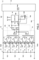
- FIG. 3 shows a block circuit diagram of a conversion module with the voltage balance function according to a first embodiment of the present disclosure, and also refer to FIG. 2 .
- the conversion module 1-1 includes an input end 12, an auxiliary power circuit 14, a power stage circuit 16, and a control unit 18.
- the input end 12 receives the input voltage Vin1, and incudes a plurality (even number) of energy storage units 122 coupled in series, such as four energy storage units 122 shown in FIG. 3 , but the present disclosure is not limited by this.
- the energy storage unit 122 may be a single capacitor or a plurality of capacitor assemblies coupled in series.
- Each energy storage unit 122 includes a first end A and a second end B, and the plurality of energy storage units 122 are coupled in series with the first end A as the head (front) and the second end B as the tail (rear).
- the sum of a plurality of energy storage voltages Vb1-Vb4 of the energy storage units 122 is the input voltage Vin1.
- the auxiliary power circuit 14 is coupled to the input end 12 and the control unit 18, and is used to convert the input voltage Vin1 to supply power to the control unit 18.
- the power stage circuit 16 may generally be a switching power conversion circuit, and the interior thereof is usually composed of components such as, but not limited to, switches, capacitors, and inductors.
- the power stage circuit 16 may be a neutral point clamped (NPC) (for example, three-level, five-level) conversion circuit, which is commonly used in high-power applications, especially applications with a power of several million watts.
- NPC neutral point clamped
- the power stage circuit 16 is coupled to the input end 12, and the control unit 18 is coupled to the switch/switches inside the power stage circuit 16.
- the control unit 18 provides a first control signal assembly Sg1 to control the switching of the switch/switches so as to control the power stage circuit 16 to convert the input voltage Vin1 into the voltage required by other rear-stage circuits.
- the power stage circuit 16 includes a first bus terminal 162, a second bus terminal 164, and a potential terminal 166.
- the first bus terminal 162 is coupled to the first end A of the first series-connected energy storage unit 122, and the second bus terminal 164 is coupled to the second end B of the last series-connected energy storage unit 122.
- the power stage circuit 16 is a five-level conversion circuit, the power stage circuit 16 includes one first bus terminal 162, one second bus terminal 164, and three potential terminals 166-1 to 166-3.
- the auxiliary power circuit 14 includes a plurality (even number) of primary-side circuits 142 and a secondary-side circuit 144, for example, four primary-side circuits 142 and one secondary-side circuit 144 as shown in FIG. 3 , but the present disclosure is not limited by this.
- the primary-side circuits 142 are coupled to the input end 12, and each primary-side circuit 142 includes a first switch unit Q1, a second switch unit Q2, and a resonance tank Rt.
- the secondary-side circuit 144 is coupled to the control unit 18, and the secondary-side circuit 144 includes a plurality of induction units Us1-Us2 and a rectification circuit Br.
- the first switch unit Q1 includes a first end and a second end, and the first end is correspondingly coupled to the first end A of one of the energy storage units 122.
- the second switch unit Q2 includes a first end and a second end, and the first end is coupled to the second end of the first switch unit Q1, and the second end is correspondingly coupled to the second end of the same energy storage unit 122.
- the resonance tank Rt is connected in parallel to the second switch unit Q2, and two primary-side circuits 142 are formed/integrated into one primary-side module 142G.
- the potential terminal 166 is coupled to a node P between two primary-side modules 142G.
- the resonance tanks Rt of the same primary-side modules 142G have corresponding circuit structures and the same parameters.
- FIG. 4 shows a circuit diagram of a primary-side module according to the present disclosure.
- the resonance tank Rt includes a capacitor Cr, an inductor Lr, and a first winding Np1/Np2.
- a first end of the capacitor Cr is coupled to the second end of the first switch unit Q1, and a first end of the inductor Lr is coupled to a second end of the capacitor Cr.
- a first end of the first winding Np1(Np2) is coupled to a second end of the inductor Lr, and a second end of the first winding Np1(Np2) is coupled to a second end of the second switch unit Q2.
- the first windings Np1,Np2 of the two resonance tanks Rt have a common-core circuit structure so that the two resonance tanks Rt can be coupled and transfer (deliver) energy to each other.
- the resonance tanks Rt used by the two primary-side circuits 142 of the primary-side module 142G have a symmetrical circuit structure and the same parameters, and therefore the first switch unit Q1 and the second switch unit Q2 can be complementarily switched by the constant frequency and the constant duty cycle so that the energy storage voltages Vb1,Vb2 naturally transfer energy to each other according to the voltage level.
- the duty cycle is preferably 50%, and the frequency may be determined according to actual circuit requirements (for example, but not limited to 50 kHz).
- the first winding Np2 may directly couple energy to the first winding Np1 through the common (iron) core so that the energy storage unit 122 corresponding to the energy storage voltage Vb1 is quickly stored energy and charged (and vice versa).
- the parameters of the resonance tank Rt includes a capacitance of the capacitor Cr, an inductance of the inductor Lr, and turns of the first windings Np1,Np2.
- the types of parameters included will vary according to the structure of the resonance tank Rt.
- the parameters of the resonant tank Rt and the control logic of the first switch unit Q1 and the second switch unit Q2 of the two primary-side circuits 142 in the same primary-side module 142G should be the same.
- the signals of controlling the first switch unit Q1 and the second switch unit Q2 may be provided by an external circuit/device outside the power supply system 100, an additional controller (not shown) inside the power supply system 100, or the control unit 18 of controlling the power stage circuit 16.
- the control unit 18 further provides a second control signal assembly Sg2 for controlling the first switch unit Q1 and the second switch unit Q2.
- the second control signal assembly Sg2 includes a first control signal Sc1 and a second control signal Sc2, and the first control signal Sc1 is used to control the first switch unit Q1 and the second control signal Sc2 is used to control the second switch unit Q2.
- the first control signal Sc1 and the second control signal Sc2 are complementary, and a frequency and a duty cycle are constant.
- the induction units Us1,Us2 are coupled in parallel, and respectively coupled to the resonance tanks Rt of the two primary-side circuits 142 in the primary-side module 142G so as to form a balance circuit 15 having the induction units Us1,Us2 and two or more primary-side modules 142G.
- the induction unit Us1 and the first windings Np1,Np2 are common-core
- the induction unit Us2 and the first windings Np3,Np4 are common-core.
- the energy of the energy storage voltages Vb1-Vb4 can be directly coupled to the lower energy party through the induction unit Us1,Us2 in parallel (under the premise of not being limited to a common core for all windings) so that the energy storage unit 122 with lower energy can be quickly stored and charged. Accordingly, the advantage of the circuit structure and control method of the auxiliary power circuit 14 in FIG. 3 is that the excessively high energy can be recycled and used in a coupling manner, instead of being consumed by a resistor (causing additional power loss, heat dissipation, component cost, etc.) and the response speed is faster.
- the energy of the energy storage voltage Vb1 is lower than the energy storage voltages Vb2-Vb4, the energy of the energy storage voltages Vb3,Vb4 is directly coupled to the induction unit Us1 through the parallel-connected induction unit Us2 with the induction unit Us1, and is coupled to the first winding Np1 through the induction unit Us1 and the first winding Np1 with the common-core circuit structure.
- the energy of the energy storage voltage Vb2 is coupled to the first winding Np1 through the first winding Np2 and the first winding Np1 with the common-core circuit structure.
- the energy storage unit 122 corresponding to the energy storage voltage Vb1 can be quickly stored energy and charged according to the characteristics of the energy storage voltages Vb1-Vb4 that the energy is naturally transferred (delivered) to each other.
- the balance circuit 15 needs to transfer energy between two or more primary-side modules 142G, the number of primary-side circuits 142 is at least four, and the number of the induction units Us1,Us2 corresponding to the primary-side modules 142G is plural.
- the rectification circuit Br is coupled to the induction units Us1-Us2 and the control unit 18, and is used to rectify the power provided by the induction units Us1-Us2 into a DC power Vdc and provide the DC power Vdc to supply power to the control unit 18.
- the rectification circuit Br and the control unit 18 are coupled to the potential terminal 166 or the second bus terminal 164 to use the potential of the potential terminal 166 or the potential of the second bus terminal 164 as a reference potential. In particular, if the second bus terminal 164 is coupled, the reference potential is the ground potential.
- the power stage circuit 16 is a five-level conversion circuit and has three potential terminals 166-1 to 166-3, the rectification circuit Br and the control unit 18 may be selectively coupled to one of the potential terminals 166-1 to 166-3.
- the auxiliary power circuit 14 further includes a module balance circuit 146.
- the module balance circuit 146 is coupled in parallel to the rectification circuit Br, and the module balance circuit 146 includes a switch SW and an energy consumption unit R.
- a first end of the switch SW is coupled to a first end of the rectification circuit Br, a second end of the switch SW is coupled to a first end of the energy consumption unit R, and a second end of the energy consumption unit R is coupled to a second end of the rectification circuit Br.
- the switch SW is turned on when the DC power Vdc is greater than a threshold value so that the energy consumption unit R consumes the DC power Vdc.
- the energy consumption unit R is, for example, but not limited to, a component or a circuit that can consume electrical energy such as a resistor or an impedance circuit.
- the plurality of conversion modules 1-1 to 1-n of the power supply system are used to equally distribute the medium-voltage DC MVDC (refer to FIG. 2 )
- the problem that the input voltage Vin1-VinN is too high can be solved by naturally transferring energy to each other through the circuit structure shown in FIG. 3 and FIG. 4 .
- the DC power Vdc provided to the control unit 18 must generally be maintained within a specific range to make the control unit 18 normally operate, the excessive high DC power Vdc may trigger the protection mechanism of the control unit 18, thereby causing the power supply system 100 to fail. Therefore, the DC power Vdc may be maintained within a specific voltage range through the operation of the module balance circuit 146. Specifically, when the DC power Vdc supplied to the control unit 18 through the secondary-side circuit 144 is too high (that is, above the threshold), the energy consumption unit R is used to consume the DC power Vdc by turning on the switch SW so that the DC power Vdc maintains in a specific voltage range. Therefore, the excessive energy of the DC power Vdc may be consumed by the energy consumption unit R to achieve the voltage balance function of the DC power Vdc in each conversion module 1-1 to 1-n.
- the signal of controlling the switch SW may be provided by an external circuit/device outside the power supply system 100, an additional controller (not shown) inside the power supply system 100, or the control unit 18 of controlling the power stage circuit 16. If the signal of controlling the switch SW is provided by the control unit 18 of controlling the power stage circuit 16, the control unit 18 sets a threshold value and detects the DC power Vdc to control the switch SW to be turned on or turned off according to whether the DC power Vdc is higher than the threshold value.
- FIG. 5A shows a block circuit diagram of the conversion module with the voltage balance function according to a second embodiment of the present disclosure
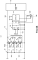
- FIG. 5B shows a block circuit diagram of the conversion module with the voltage balance function according to a third embodiment of the present disclosure, and also refer to FIG. 2 to FIG. 4 .
- the embodiment of FIG. 5A shows that the power stage circuit 16 is a five-level conversion circuit, and therefore the power stage circuit 16 includes a first bus terminal 162, a second bus terminal 164, and three potential terminals 166-1 to 166-3.
- the secondary-side circuit 144 includes a plurality of induction units Us1-Us4 and a rectification circuit Br.
- the symmetrical resonance tank circuits allow energy to naturally transfer (deliver) to each other so that the energy storage voltages Vb1-Vb8 corresponding to the energy storage units 122 may be maintained in balance.
- the embodiment of FIG. 5B shows that the power stage circuit 16 is a single-level conversion circuit, and therefore the power stage circuit 16 includes a first bus terminal 162 and a second bus terminal 164.
- One primary-side module 142G is coupled between the first bus terminal 162 and the second bus terminal 164, and the secondary-side circuit 144 includes one induction unit Us1 and a rectification circuit Br.
- the symmetrical resonance tank circuits allow energy to naturally transfer (deliver) to each other so that the energy storage voltages Vb1-Vb2 corresponding to the energy storage units 122 may be maintained in balance.
- FIG. 6A shows a circuit diagram of a balance circuit according to a first embodiment of the present disclosure
- FIG. 6B shows a circuit diagram of the balance circuit according to a second embodiment of the present disclosure, and also refer to FIG. 1 to FIG. 5B .
- FIG. 6A and FIG. 6B mainly show the implementation of the induction units Us1-Us2 cooperated with the first windings Np1-Np4 in a common-core manner.
- FIG. 6A and FIG. 6B mainly show the implementation of the induction units Us1-Us2 cooperated with the first windings Np1-Np4 in a common-core manner.
- each induction unit Us1,Us2 includes one second winding Ns1,Ns2, and the second winding Ns1 and the first windings Np1,Np2 of the two primary-side circuits 142 in one primary-side module 142G form a first transformer T1 with a common core, and the second winding Ns2 and the first windings Np3,Np4 of the two primary-side circuits 142 in one primary-side module 142G form a first transformer T1 with a common core.
- each induction unit Us1,Us2 includes one second winding Ns1,Ns2 and a third winding Ns3,Ns4.
- the second windings Ns1,Ns2 and the first windings Np1,Np3 of one primary-side circuit 142 form a first transformer Tlwith a common core.
- the third windings Ns3,Ns4 and the first windings Np2,Np4 of the other primary-side circuit 142 form a second transformer T2 with a common core. Since FIG. 6A integrates windings into two first transformers T1, compared to FIG. 6B , the total volume (size) of the transformer can be reduced as the number of the iron cores is reduced from four to two.
- the energy of the first windings Np1-Np2, Np3-Np4 with the common (iron) core can be directly transferred through the coupling of the primary side, without transmission through the secondary side. Therefore, the embodiment in FIG. 6A is a preferred embodiment.
Landscapes
- Engineering & Computer Science (AREA)
- Power Engineering (AREA)
- Dc-Dc Converters (AREA)
Abstract
Description
- The present disclosure relates to an auxiliary power circuit, a balance circuit, and a power supply system, and more particularly to an auxiliary power circuit of a conversion module with a voltage balance function, a balance circuit of the conversion module, and a power supply system having the conversion module.
- The statements in this section merely provide background information related to the present disclosure and do not necessarily constitute prior art.
- Please refer to
FIG. 1 , which shows a block diagram of a conventional power supply system. The currently used medium-voltage DC (MVDC)power supply system 100 includes a plurality of conversion modules 1-1 to 1-n with input terminals coupled in series. The auxiliary power supply (APS) that supplies power to the internal controller of thepower supply system 100 are mostly powered externally (indicated by the arrow pointing to the APS), rather than self-powered. The reason is that the medium-voltage DC (MVDC) is usually greater than 1500 volts, even as high as tens of kilovolts, and therefore the power supply system can usually receive the kilovolt-level medium-voltage DC. If in the form of self-powered, the auxiliary power supply APS must have the insulation capability of medium voltage isolation to convert power up to several tens of kilovolts to a power supply controller below 50 volts. Otherwise, external power supply must be required. However, these two situations are nothing more than the need to use a larger and more expensive isolation transformer, or the need for an additional power supply for powering, both increase the circuit volume and cost. - Using the auxiliary power supply APS in the form of self-powered, usually the conversion modules 1-1 to 1-n are respectively coupled to the capacitors C at the input terminal thereof to use the power stored in the capacitors C. Therefore, in addition to the insulation capability of medium voltage isolation, the auxiliary power supply APS using the self-powered
auxiliary power circuit 100 must also maintain a voltage balance of the power at the input terminals of the conversion modules 1-1 to 1-n so as to avoid the rear-stage controller (or other circuits, etc.) of each conversion module 1-1 to 1-n from entering the protection state due to overvoltage condition. Therefore, an additional voltage balance circuit must be added (which leads to an increase in circuit volume and cost) and the present voltage balance circuit is also unable to perform rapid voltage balance control on the capacitors C. - Accordingly, the present disclosure is to provide an auxiliary power circuit, a balance circuit, and a power supply system to make the energy storage voltages of the energy storage units naturally transfer energy to each other according to the voltage level, and the excessively high energy can be recycled and used in a coupling manner.
- In order to solve the above-mentioned problems, the present disclosure provides an auxiliary power circuit of a conversion module for supplying power to a control unit. An input end of the conversion module includes an even number of energy storage units coupled in series, and each energy storage unit includes a first end and a second end. The auxiliary power circuit includes an even number of primary-side circuits and a secondary-side circuit. Each primary-side circuit includes a first switch unit, a second switch unit, and a resonance tank. The first switch unit includes a first end and a second end, and the first end of the first switch unit is correspondingly coupled to the first end of one of the energy storage units. The second switch unit includes a first end and a second end, and the first end of the second switch unit is coupled to the second end of the first switch unit, and the second end of the second switch unit is correspondingly coupled to the second end of one of the energy storage units. The resonance tank is coupled in parallel to the second switch unit. The secondary-side circuit includes at least one induction unit and a rectification circuit. The at least one induction unit is coupled to the two resonance tanks of the two primary-side circuits. The rectification circuit is coupled to the at least one induction unit and the control unit, and rectifies a power provided by the at least one induction unit into a DC power and supply the DC power to the control unit.
- In order to solve the above-mentioned problems, the present disclosure provides a balance circuit of a conversion module. An input end of the conversion module includes an even number of energy storage units coupled in series, and each energy storage unit includes a first end and a second end. The balance circuit includes an even number of primary-side circuits and a secondary-side circuit. Each primary-side circuit includes a first switch unit, a second switch unit, and a resonance tank. The first switch unit includes a first end and a second end, and the first end of the first switch unit is correspondingly coupled to the first end of one of the energy storage units. The second switch unit includes a first end and a second end, and the first end of the second switch unit is coupled to the second end of the first switch unit, and the second end of the second switch unit is correspondingly coupled to the second end of one of the energy storage units. The resonance tank is coupled in parallel to the second switch unit. The secondary-side circuit includes a plurality of induction units coupled in parallel to each other, and respectively coupled to the two resonance tanks of the two primary-side circuits. The number of the primary-side circuits is at least four.
- In order to solve the above-mentioned problems, the present disclosure provides a power supply system. The power supply system includes a plurality of conversion modules, and each conversion module includes an input end, and the input ends of the plurality of conversion modules are coupled in series. The input end includes an even number of energy storage units coupled in series, and each energy storage unit includes a first end and a second end. Each conversion module includes an auxiliary power circuit, a power stage circuit, and a control unit. The auxiliary power circuit includes an even number of primary-side circuits and a secondary-side circuit. Each primary-side circuit includes a first switch unit, a second switch unit, and a resonance tank. The first switch unit includes a first end and a second end, and the first end of the first switch unit is correspondingly coupled to the first end of one of the energy storage units. The second switch unit includes a first end and a second end, and the first end of the second switch unit is coupled to the second end of the first switch unit, and the second end of the second switch unit is correspondingly coupled to the second end of one of the energy storage units. The resonance tank is coupled in parallel to the second switch unit. The secondary-side circuit includes at least one induction unit and a rectification circuit. The at least one induction unit is coupled to the two resonance tanks of the two primary-side circuits. The rectification circuit is coupled to the at least one induction unit, and rectifies a power provided by the at least one induction unit into a DC power. The power stage circuit is coupled to the input end. The control unit is coupled to the rectification circuit and the power stage circuit, and receives the DC power to operate and to control the power stage circuit.
- The main purpose and effect of the present disclosure is that the resonance tanks used by the two primary-side circuits of the primary-side module have a symmetrical circuit structure and the same parameters, and therefore the energy storage voltages of the energy storage units naturally transfer energy to each other according to the voltage level, and the excessively high energy can be recycled and used in a coupling manner and the response speed is also faster since the power consumption is not performed by resistors.
- It is to be understood that both the foregoing general description and the following detailed description are exemplary, and are intended to provide further explanation of the present disclosure as claimed. Other advantages and features of the present disclosure will be apparent from the following description, drawings and claims.
- The present disclosure can be more fully understood by reading the following detailed description of the embodiment, with reference made to the accompanying drawing as follows:
-
FIG. 1 is a block diagram of a conventional power supply system. -
FIG. 2 is a block diagram of a power supply system with a voltage balance function according to the present disclosure. -
FIG. 3 is a block circuit diagram of a conversion module with the voltage balance function according to a first embodiment of the present disclosure. -
FIG. 4 is a circuit diagram of a primary-side module according to the present disclosure. -
FIG. 5A is a block circuit diagram of the conversion module with the voltage balance function according to a second embodiment of the present disclosure. -
FIG. 5B is a block circuit diagram of the conversion module with the voltage balance function according to a third embodiment of the present disclosure. -
FIG. 6A is a circuit diagram of a balance circuit according to a first embodiment of the present disclosure. -
FIG. 6B is a circuit diagram of the balance circuit according to a second embodiment of the present disclosure. - Reference will now be made to the drawing figures to describe the present disclosure in detail. It will be understood that the drawing figures and exemplified embodiments of present disclosure are not limited to the details thereof.
- Please refer to
FIG. 2 , which shows a block diagram of a power supply system with a voltage balance function according to the present disclosure. Thepower supply system 100 is mainly applied to a solid state transformer (SST), also known as a power electronic transformer. Thepower supply system 100 receives a medium-voltage DC MVDC. In such a high voltage application, an input end of thepower supply system 100 includes a plurality of capacitors C coupled in series to stabilize (regulate) the voltage value of the medium-voltage DC MVDC, and a plurality of conversion modules 1-1 to 1-n are used to equally distribute (share) the medium-voltage DC MVDC. Specifically, thepower supply system 100 includes a plurality of conversion modules 1-1 to 1-n, and a plurality of input ends of the plurality of conversion modules 1-1 to 1-n are coupled in series to equally distribute the medium-voltage DC MVDC. That is, the voltage value of the medium-voltage DC MVDC (namely a voltage across a plurality of capacitors C coupled in series) is the sum of a plurality of input voltages Vin1-VinN of the plurality of conversion modules 1-1 to 1-n. The output ends (not shown) of the conversion modules 1-1 to 1-n may be coupled in series, coupled in parallel, or independently output, which is not limited here. - Please refer to
FIG. 3 , which shows a block circuit diagram of a conversion module with the voltage balance function according to a first embodiment of the present disclosure, and also refer toFIG. 2 . Take the conversion module 1-1 as an example, the conversion module 1-1 includes aninput end 12, anauxiliary power circuit 14, apower stage circuit 16, and acontrol unit 18. Theinput end 12 receives the input voltage Vin1, and incudes a plurality (even number) ofenergy storage units 122 coupled in series, such as fourenergy storage units 122 shown inFIG. 3 , but the present disclosure is not limited by this. In particular, theenergy storage unit 122 may be a single capacitor or a plurality of capacitor assemblies coupled in series. Eachenergy storage unit 122 includes a first end A and a second end B, and the plurality ofenergy storage units 122 are coupled in series with the first end A as the head (front) and the second end B as the tail (rear). The sum of a plurality of energy storage voltages Vb1-Vb4 of theenergy storage units 122 is the input voltage Vin1. Theauxiliary power circuit 14 is coupled to theinput end 12 and thecontrol unit 18, and is used to convert the input voltage Vin1 to supply power to thecontrol unit 18. Thepower stage circuit 16 may generally be a switching power conversion circuit, and the interior thereof is usually composed of components such as, but not limited to, switches, capacitors, and inductors. For example, but not limited to, thepower stage circuit 16 may be a neutral point clamped (NPC) (for example, three-level, five-level) conversion circuit, which is commonly used in high-power applications, especially applications with a power of several million watts. - The
power stage circuit 16 is coupled to theinput end 12, and thecontrol unit 18 is coupled to the switch/switches inside thepower stage circuit 16. Thecontrol unit 18 provides a first control signal assembly Sg1 to control the switching of the switch/switches so as to control thepower stage circuit 16 to convert the input voltage Vin1 into the voltage required by other rear-stage circuits. Take a three-level conversion circuit as an example, thepower stage circuit 16 includes afirst bus terminal 162, asecond bus terminal 164, and apotential terminal 166. Thefirst bus terminal 162 is coupled to the first end A of the first series-connectedenergy storage unit 122, and thesecond bus terminal 164 is coupled to the second end B of the last series-connectedenergy storage unit 122. If thepower stage circuit 16 is a five-level conversion circuit, thepower stage circuit 16 includes onefirst bus terminal 162, onesecond bus terminal 164, and three potential terminals 166-1 to 166-3. - The
auxiliary power circuit 14 includes a plurality (even number) of primary-side circuits 142 and a secondary-side circuit 144, for example, four primary-side circuits 142 and one secondary-side circuit 144 as shown inFIG. 3 , but the present disclosure is not limited by this. The primary-side circuits 142 are coupled to theinput end 12, and each primary-side circuit 142 includes a first switch unit Q1, a second switch unit Q2, and a resonance tank Rt. The secondary-side circuit 144 is coupled to thecontrol unit 18, and the secondary-side circuit 144 includes a plurality of induction units Us1-Us2 and a rectification circuit Br. The first switch unit Q1 includes a first end and a second end, and the first end is correspondingly coupled to the first end A of one of theenergy storage units 122. The second switch unit Q2 includes a first end and a second end, and the first end is coupled to the second end of the first switch unit Q1, and the second end is correspondingly coupled to the second end of the sameenergy storage unit 122. The resonance tank Rt is connected in parallel to the second switch unit Q2, and two primary-side circuits 142 are formed/integrated into one primary-side module 142G. Thepotential terminal 166 is coupled to a node P between two primary-side modules 142G. The resonance tanks Rt of the same primary-side modules 142G have corresponding circuit structures and the same parameters. - Please refer to
FIG. 4 , which shows a circuit diagram of a primary-side module according to the present disclosure. Take a single primary-side module 142G inFIG. 3 as an example. The resonance tank Rt includes a capacitor Cr, an inductor Lr, and a first winding Np1/Np2. A first end of the capacitor Cr is coupled to the second end of the first switch unit Q1, and a first end of the inductor Lr is coupled to a second end of the capacitor Cr. A first end of the first winding Np1(Np2) is coupled to a second end of the inductor Lr, and a second end of the first winding Np1(Np2) is coupled to a second end of the second switch unit Q2. In the primary-side module 142G, the first windings Np1,Np2 of the two resonance tanks Rt have a common-core circuit structure so that the two resonance tanks Rt can be coupled and transfer (deliver) energy to each other. Specifically, take the primary-side circuits 142 corresponding to the energystorage voltages Vb 1,Vb2 having the common-core circuit structure as an example. The resonance tanks Rt used by the two primary-side circuits 142 of the primary-side module 142G have a symmetrical circuit structure and the same parameters, and therefore the first switch unit Q1 and the second switch unit Q2 can be complementarily switched by the constant frequency and the constant duty cycle so that the energy storage voltages Vb1,Vb2 naturally transfer energy to each other according to the voltage level. In one embodiment, the duty cycle is preferably 50%, and the frequency may be determined according to actual circuit requirements (for example, but not limited to 50 kHz). - When the energy storage voltage Vb1 is lower, the first winding Np2 may directly couple energy to the first winding Np1 through the common (iron) core so that the
energy storage unit 122 corresponding to the energy storage voltage Vb1 is quickly stored energy and charged (and vice versa). TakeFIG. 4 as an example, the parameters of the resonance tank Rt includes a capacitance of the capacitor Cr, an inductance of the inductor Lr, and turns of the first windings Np1,Np2. However, the types of parameters included will vary according to the structure of the resonance tank Rt. Mainly, the parameters of the resonant tank Rt and the control logic of the first switch unit Q1 and the second switch unit Q2 of the two primary-side circuits 142 in the same primary-side module 142G should be the same. In one embodiment, the signals of controlling the first switch unit Q1 and the second switch unit Q2 may be provided by an external circuit/device outside thepower supply system 100, an additional controller (not shown) inside thepower supply system 100, or thecontrol unit 18 of controlling thepower stage circuit 16. - If the signals of controlling the first switch unit Q1 and the second switch unit Q2 are provided by the
control unit 18 of controlling thepower stage circuit 16, besides the first control signal assembly Sg1 of controlling thepower stage circuit 16, thecontrol unit 18 further provides a second control signal assembly Sg2 for controlling the first switch unit Q1 and the second switch unit Q2. The second control signal assembly Sg2 includes a first control signal Sc1 and a second control signal Sc2, and the first control signal Sc1 is used to control the first switch unit Q1 and the second control signal Sc2 is used to control the second switch unit Q2. In particular, the first control signal Sc1 and the second control signal Sc2 are complementary, and a frequency and a duty cycle are constant. - Please refer to
FIG. 3 andFIG. 4 again, the induction units Us1,Us2 are coupled in parallel, and respectively coupled to the resonance tanks Rt of the two primary-side circuits 142 in the primary-side module 142G so as to form abalance circuit 15 having the induction units Us1,Us2 and two or more primary-side modules 142G. Specifically, the induction unit Us1 and the first windings Np1,Np2 are common-core, and the induction unit Us2 and the first windings Np3,Np4 are common-core. Since the induction units Us1,Us2 are coupled in parallel, the energy of the energy storage voltages Vb1-Vb4 can be directly coupled to the lower energy party through the induction unit Us1,Us2 in parallel (under the premise of not being limited to a common core for all windings) so that theenergy storage unit 122 with lower energy can be quickly stored and charged. Accordingly, the advantage of the circuit structure and control method of theauxiliary power circuit 14 inFIG. 3 is that the excessively high energy can be recycled and used in a coupling manner, instead of being consumed by a resistor (causing additional power loss, heat dissipation, component cost, etc.) and the response speed is faster. - If the energy of the energy storage voltage Vb1 is lower than the energy storage voltages Vb2-Vb4, the energy of the energy storage voltages Vb3,Vb4 is directly coupled to the induction unit Us1 through the parallel-connected induction unit Us2 with the induction unit Us1, and is coupled to the first winding Np1 through the induction unit Us1 and the first winding Np1 with the common-core circuit structure. Similarly, the energy of the energy storage voltage Vb2 is coupled to the first winding Np1 through the first winding Np2 and the first winding Np1 with the common-core circuit structure. Therefore, the
energy storage unit 122 corresponding to the energy storage voltage Vb1 can be quickly stored energy and charged according to the characteristics of the energy storage voltages Vb1-Vb4 that the energy is naturally transferred (delivered) to each other. In one embodiment, since thebalance circuit 15 needs to transfer energy between two or more primary-side modules 142G, the number of primary-side circuits 142 is at least four, and the number of the induction units Us1,Us2 corresponding to the primary-side modules 142G is plural. - The rectification circuit Br is coupled to the induction units Us1-Us2 and the
control unit 18, and is used to rectify the power provided by the induction units Us1-Us2 into a DC power Vdc and provide the DC power Vdc to supply power to thecontrol unit 18. The rectification circuit Br and thecontrol unit 18 are coupled to thepotential terminal 166 or thesecond bus terminal 164 to use the potential of thepotential terminal 166 or the potential of thesecond bus terminal 164 as a reference potential. In particular, if thesecond bus terminal 164 is coupled, the reference potential is the ground potential. On the other hand, if thepower stage circuit 16 is a five-level conversion circuit and has three potential terminals 166-1 to 166-3, the rectification circuit Br and thecontrol unit 18 may be selectively coupled to one of the potential terminals 166-1 to 166-3. - Please refer to
FIG. 3 again, theauxiliary power circuit 14 further includes amodule balance circuit 146. Themodule balance circuit 146 is coupled in parallel to the rectification circuit Br, and themodule balance circuit 146 includes a switch SW and an energy consumption unit R. A first end of the switch SW is coupled to a first end of the rectification circuit Br, a second end of the switch SW is coupled to a first end of the energy consumption unit R, and a second end of the energy consumption unit R is coupled to a second end of the rectification circuit Br. The switch SW is turned on when the DC power Vdc is greater than a threshold value so that the energy consumption unit R consumes the DC power Vdc. In particular, the energy consumption unit R is, for example, but not limited to, a component or a circuit that can consume electrical energy such as a resistor or an impedance circuit. Specifically, since the plurality of conversion modules 1-1 to 1-n of the power supply system are used to equally distribute the medium-voltage DC MVDC (refer toFIG. 2 ), there is a problem of voltage balance of the input voltages Vin1-VinN of the corresponding conversion modules 1-1 to 1-n. That is, the input voltage Vin1-VinN of a certain conversion module 1-1 to 1-n is too high. In particular, the problem that the input voltage Vin1-VinN is too high can be solved by naturally transferring energy to each other through the circuit structure shown inFIG. 3 andFIG. 4 . - However, since the DC power Vdc provided to the
control unit 18 must generally be maintained within a specific range to make thecontrol unit 18 normally operate, the excessive high DC power Vdc may trigger the protection mechanism of thecontrol unit 18, thereby causing thepower supply system 100 to fail. Therefore, the DC power Vdc may be maintained within a specific voltage range through the operation of themodule balance circuit 146. Specifically, when the DC power Vdc supplied to thecontrol unit 18 through the secondary-side circuit 144 is too high (that is, above the threshold), the energy consumption unit R is used to consume the DC power Vdc by turning on the switch SW so that the DC power Vdc maintains in a specific voltage range. Therefore, the excessive energy of the DC power Vdc may be consumed by the energy consumption unit R to achieve the voltage balance function of the DC power Vdc in each conversion module 1-1 to 1-n. - In one embodiment, the signal of controlling the switch SW may be provided by an external circuit/device outside the
power supply system 100, an additional controller (not shown) inside thepower supply system 100, or thecontrol unit 18 of controlling thepower stage circuit 16. If the signal of controlling the switch SW is provided by thecontrol unit 18 of controlling thepower stage circuit 16, thecontrol unit 18 sets a threshold value and detects the DC power Vdc to control the switch SW to be turned on or turned off according to whether the DC power Vdc is higher than the threshold value. - Please refer to
FIG. 5A , which shows a block circuit diagram of the conversion module with the voltage balance function according to a second embodiment of the present disclosure; please refer toFIG. 5B , which shows a block circuit diagram of the conversion module with the voltage balance function according to a third embodiment of the present disclosure, and also refer toFIG. 2 to FIG. 4 . Compared withFIG. 3 , the embodiment ofFIG. 5A shows that thepower stage circuit 16 is a five-level conversion circuit, and therefore thepower stage circuit 16 includes afirst bus terminal 162, asecond bus terminal 164, and three potential terminals 166-1 to 166-3. There is one primary-side module 142G is disposed (coupled) between the two potentials, and the secondary-side circuit 144 includes a plurality of induction units Us1-Us4 and a rectification circuit Br. In this embodiment, the symmetrical resonance tank circuits allow energy to naturally transfer (deliver) to each other so that the energy storage voltages Vb1-Vb8 corresponding to theenergy storage units 122 may be maintained in balance. - Compared with
FIG. 3 , the embodiment ofFIG. 5B shows that thepower stage circuit 16 is a single-level conversion circuit, and therefore thepower stage circuit 16 includes afirst bus terminal 162 and asecond bus terminal 164. One primary-side module 142G is coupled between thefirst bus terminal 162 and thesecond bus terminal 164, and the secondary-side circuit 144 includes one induction unit Us1 and a rectification circuit Br. In this embodiment, the symmetrical resonance tank circuits allow energy to naturally transfer (deliver) to each other so that the energy storage voltages Vb1-Vb2 corresponding to theenergy storage units 122 may be maintained in balance. - Please refer to
FIG. 6A , which shows a circuit diagram of a balance circuit according to a first embodiment of the present disclosure; please refer toFIG. 6B , which shows a circuit diagram of the balance circuit according to a second embodiment of the present disclosure, and also refer toFIG. 1 to FIG. 5B .FIG. 6A andFIG. 6B mainly show the implementation of the induction units Us1-Us2 cooperated with the first windings Np1-Np4 in a common-core manner. InFIG. 6A , each induction unit Us1,Us2 includes one second winding Ns1,Ns2, and the second winding Ns1 and the first windings Np1,Np2 of the two primary-side circuits 142 in one primary-side module 142G form a first transformer T1 with a common core, and the second winding Ns2 and the first windings Np3,Np4 of the two primary-side circuits 142 in one primary-side module 142G form a first transformer T1 with a common core. As shown inFIG. 6B , each induction unit Us1,Us2 includes one second winding Ns1,Ns2 and a third winding Ns3,Ns4. The second windings Ns1,Ns2 and the first windings Np1,Np3 of one primary-side circuit 142 form a first transformer Tlwith a common core. The third windings Ns3,Ns4 and the first windings Np2,Np4 of the other primary-side circuit 142 form a second transformer T2 with a common core. SinceFIG. 6A integrates windings into two first transformers T1, compared toFIG. 6B , the total volume (size) of the transformer can be reduced as the number of the iron cores is reduced from four to two. Also, the energy of the first windings Np1-Np2, Np3-Np4 with the common (iron) core can be directly transferred through the coupling of the primary side, without transmission through the secondary side. Therefore, the embodiment inFIG. 6A is a preferred embodiment.
Claims (15)
- An auxiliary power circuit (14) of a conversion module (1-1 to 1-n) configured for supplying power to a control unit (18), an input end of the conversion module (1-1 to 1-n) comprising an even number of energy storage units (122) coupled in series, and each energy storage unit (122) comprising a first end (A) and a second end (B), characterized in that the auxiliary power circuit (14) comprising:an even number of primary-side circuits (142), and each primary-side circuit (142) comprising:a first switch unit (Q1) comprising a first end and a second end, and the first end of the first switch unit (Q1) correspondingly coupled to the first end (A) of one of the energy storage units (122),a second switch unit (Q2) comprising a first end and a second end, and the first end of the second switch unit (Q2) coupled to the second end of the first switch unit (Q1), and the second end of the second switch unit (Q2) correspondingly coupled to the second end (B) of one of the energy storage units (122), anda resonance tank (Rt) coupled in parallel to the second switch unit (Q2), anda secondary-side circuit (144) comprising:at least one induction unit (Us1-Us2) coupled to the two resonance tanks (Rt) of the two primary-side circuits (142), anda rectification circuit (Br) coupled to the at least one induction unit (Us1-Us2) and the control unit (18), and configured to rectify a power provided by the at least one induction unit (Us1-Us2) into a DC power (Vdc) and supply the DC power (Vdc) to the control unit (18).
- The auxiliary power circuit (14) as claimed in claim 1, further comprising:
a module balance circuit (146) coupled in parallel to the rectification circuit (Br), and the module balance circuit (146) comprising:a switch (SW) coupled to the rectification circuit (Br), and configured to be turned on according to the DC power (Vdc) being higher than a threshold value, andan energy consumption unit (R) coupled in series to the switch (SW), and configured to consume the DC power (Vdc) when the switch (SW) is turned on. - The auxiliary power circuit (14) as claimed in claim 1, wherein the resonance tank (Rt) comprises a capacitor (Cr), an inductor (Lr), and a first winding (Np1-Np4) coupled in series, andwherein the resonance tank (Rt) of each primary-side circuit (142) comprises a parameter, and the parameters of the two resonance tanks (Rt) of the two primary-side circuits (142) are the same,wherein the parameter comprises a capacitance of the capacitor (Cr), an inductance of the inductor (Lr), and a turn of the first winding (Np1-Np4).
- The auxiliary power circuit (14) as claimed in claim 3, wherein the at least one induction unit (Us1-Us2) comprises a second winding (Ns1-Ns2),
wherein the second winding (Ns1-Ns2) and the two first windings (Np1-Np4) of the two primary-side circuits (142) form a first transformer (T1) with a common core. - The auxiliary power circuit (14) as claimed in claim 3, wherein the at least one induction unit (Us1-Us2) comprises a second winding (Ns1-Ns2) and a third winding (Ns3-Ns4),
wherein the second winding (Ns1-Ns2) and the first winding (Np1-Np4) of one of the two primary-side circuits (142) form a first transformer (T1) with a common core, and the third winding (Ns3-Ns4) and the first winding (Np1-Np4) of the other of the two primary-side circuits (142) form a second transformer (T2) with a common core. - The auxiliary power circuit (14) as claimed in claim 1, wherein the first switch unit (Q1) and the second switch unit (Q2) are complementarily switched at a frequency and a duty cycle, and the frequency and the duty cycle are constant.
- A balance circuit (15) of a conversion module (1-1 to 1-n), an input end of the conversion module (1-1 to 1-n) comprising an even number of energy storage units (122) coupled in series, and each energy storage unit (122) comprising a first end (A) and a second end (B), characterized in that the balance circuit (15) comprising:an even number of primary-side circuits (142), and each primary-side circuit (142) comprising:a first switch unit (Q1) comprising a first end and a second end, and the first end of the first switch unit (Q1) correspondingly coupled to the first end (A) of one of the energy storage units (122),a second switch unit (Q2) comprising a first end and a second end, and the first end of the second switch unit (Q2) coupled to the second end of the first switch unit (Q1), and the second end of the second switch unit (Q2) correspondingly coupled to the second end (B) of one of the energy storage units (122), anda resonance tank (Rt) coupled in parallel to the second switch unit (Q2), anda secondary-side circuit (144) comprising:a plurality of induction units (Us1-Us2) coupled in parallel to each other, and respectively coupled to the two resonance tanks (Rt) of the two primary-side circuits (142),wherein the number of the primary-side circuits (142) is at least four.
- The balance circuit (15) as claimed in claim 7, wherein the resonance tank (Rt) comprises: a capacitor (Cr), an inductor (Lr), and a first winding (Np1-Np4) coupled in series, andwherein the resonance tank (Rt) of each primary-side circuit (142) comprises a parameter, and the parameters of the two resonance tanks (Rt) of the two primary-side circuits (142) are the same,wherein the parameter comprises a capacitance of the capacitor (Cr), an inductance of the inductor (Lr), and a turn of the first winding (Np1-Np4).
- The balance circuit (15) as claimed in claim 8, wherein each induction unit (Us1-Us2) comprises a second winding (Ns1-Ns2),
wherein the second winding (Ns1-Ns2) and the two first windings (Np1-Np4) of the two primary-side circuits (142) form a first transformer (T1) with a common core. - The balance circuit (15) as claimed in claim 8, wherein each induction unit (Us1-Us2) comprises a second winding (Ns1-Ns2) and a third winding (Ns3-Ns4),
wherein the second winding (Ns1-Ns2) and the first winding (Np1-Np4) of one of the two primary-side circuits (142) form a first transformer (T1) with a common core, and the third winding (Ns3-Ns4) and the first winding (Np1-Np4) of the other of the two primary-side circuits (142) form a second transformer (T2) with a common core. - The balance circuit (15) as claimed in claim 7, wherein the first switch unit (Q1) and the second switch unit (Q2) are complementarily switched at a frequency and a duty cycle, and the frequency and the duty cycle are constant.
- A power supply system (100), characterized in that the power supply system (100) comprising:
a plurality of conversion modules (1-1 to 1-n), each conversion module (1-1 to 1-n) comprising an input end (12), and the input ends (12) of the plurality of conversion modules (1-1 to 1-n) coupled in series, the input end (12) comprising an even number of energy storage units (122) coupled in series, and each energy storage unit (122) comprising a first end (A) and a second end (B), each conversion module (1-1 to 1-n) comprising:an auxiliary power circuit (14) comprising:an even number of primary-side circuits (142), and each primary-side circuit (142) comprising:a first switch unit (Q1) comprising a first end and a second end, and the first end of the first switch unit (Q1) correspondingly coupled to the first end of one of the energy storage units (122),a second switch unit (Q2) comprising a first end and a second end, and the first end of the second switch unit (Q2) coupled to the second end of the first switch unit (Q1), and the second end of the second switch unit (Q2) correspondingly coupled to the second end of one of the energy storage units (122), anda resonance tank (Rt) coupled in parallel to the second switch unit (Q2), anda secondary-side circuit (144) comprising:at least one induction unit (Us1-Us2) coupled to the two resonance tanks (Rt) of the two primary-side circuits (142), anda rectification circuit (Br) coupled to the at least one induction unit (Us1-Us2), and configured to rectify a power provided by the at least one induction unit (Us1-Us2) into a DC power (Vdc),a power stage circuit (16) coupled to the input end, anda control unit (18) coupled to the rectification circuit (Br) and the power stage circuit (16), and configured to receive the DC power (Vdc) to operate and to control the power stage circuit (16). - The power supply system (100) as claimed in claim 12, wherein the even number of primary-side circuits (142) form a primary-side module (142G) in pairs, and the power stage circuit (16) comprises:a first bus terminal (162) coupled to the first end (A) of the first series-connected energy storage unit (122),a second bus terminal (164) coupled to the second end (B) of the last series-connected energy storage unit (122), anda potential terminal (166,166-1 to 166-3) coupled to a node (P) between two primary-side modules (142G),wherein the secondary-side circuit (144) and the control unit (18) are coupled to the potential terminal (166,166-1 to 166-3) or the second bus terminal (164) to use a potential of the potential terminal (166,166-1 to 166-3) or a potential of the second bus terminal (164) as a reference potential.
- The power supply system (100) as claimed in claim 13, wherein the auxiliary power circuit (14) further comprises:a module balance circuit (146) coupled in parallel to the rectification circuit (Br), and the module balance circuit (146) comprises:a switch (SW) coupled to the rectification circuit (Br), andan energy consumption unit (R) coupled in series to the switch (SW), and configured to consume the DC power (Vdc) when the switch (SW) is turned on,wherein the control unit (18) is configured to detect the DC power (Vdc), and control the switch (SW) to be turned on when the DC power (Vdc) is higher than a threshold value.
- The power supply system (100) as claimed in claim 12, wherein the control unit (18) is configured to provide a first control signal assembly (Sg1) to control the power stage circuit (16), and provide a second control signal assembly (Sg2) to control the first switch unit (Q1) and the second switch unit (Q2),
wherein the second control signal assembly (Sg2) comprises a first control signal (Sc1) of controlling the first switch unit (Q1) and a second control signal (Sc2) of controlling the second switch unit (Q2); the first control signal (Sc1) and the second control signal (Sc2) are complementary, and a frequency and a duty cycle of the first control signal (Sc1) and the second control signal (Sc2) are constant.
Applications Claiming Priority (1)
| Application Number | Priority Date | Filing Date | Title |
|---|---|---|---|
| CN202111326734.5A CN116111847B (en) | 2021-11-10 | 2021-11-10 | Auxiliary power supply circuit, balance circuit and power supply system of conversion module |
Publications (1)
| Publication Number | Publication Date |
|---|---|
| EP4181367A1 true EP4181367A1 (en) | 2023-05-17 |
Family
ID=81448365
Family Applications (1)
| Application Number | Title | Priority Date | Filing Date |
|---|---|---|---|
| EP22170771.4A Pending EP4181367A1 (en) | 2021-11-10 | 2022-04-29 | Auxiliary power circuit, balance circuit, and power supply system |
Country Status (3)
| Country | Link |
|---|---|
| US (2) | US12062988B2 (en) |
| EP (1) | EP4181367A1 (en) |
| CN (1) | CN116111847B (en) |
Families Citing this family (3)
| Publication number | Priority date | Publication date | Assignee | Title |
|---|---|---|---|---|
| US20230048191A1 (en) * | 2021-08-13 | 2023-02-16 | Delta Electronics, Inc. | Battery cell balance circuit and method of operating the same |
| CN116937975A (en) * | 2022-03-30 | 2023-10-24 | 英飞凌科技奥地利有限公司 | Circuit for bi-directional converter, bi-directional converter and method of operating the same |
| WO2025218913A1 (en) * | 2024-04-19 | 2025-10-23 | Huawei Digital Power Technologies Co., Ltd. | Converter and method for controlling a converter |
Citations (7)
| Publication number | Priority date | Publication date | Assignee | Title |
|---|---|---|---|---|
| DE10157003A1 (en) * | 2000-11-21 | 2002-05-23 | Fuji Jukogyo Kk Tokio | Voltage compensation device for battery units |
| US8269455B2 (en) * | 2010-09-29 | 2012-09-18 | Sendyne Corporation | Charge balancing system |
| US9231420B2 (en) * | 2011-04-19 | 2016-01-05 | Shindengen Electric Manufacturing Co., Ltd. | Cell balance circuit and cell balance device |
| WO2018061077A1 (en) * | 2016-09-27 | 2018-04-05 | 株式会社日立製作所 | Power conversion device |
| US20190149063A1 (en) * | 2016-06-15 | 2019-05-16 | Mitsubishi Electric Corporation | Electric motor drive device |
| EP2945257B1 (en) * | 2014-05-13 | 2019-11-13 | Siemens Aktiengesellschaft | Balancing electric voltages of electric capacitors connected in series |
| US11056878B2 (en) * | 2019-03-05 | 2021-07-06 | Nxp Usa, Inc. | Overvoltage protection circuit for wireless power receiver |
Family Cites Families (10)
| Publication number | Priority date | Publication date | Assignee | Title |
|---|---|---|---|---|
| US6373223B1 (en) * | 2000-11-21 | 2002-04-16 | Nagano Japan Radio Co., Ltd. | Voltage equalizing apparatus and voltage equalizing method for battery devices |
| JP2007236010A (en) * | 2006-02-02 | 2007-09-13 | Sony Corp | Switching power supply circuit |
| US7859864B2 (en) * | 2007-11-28 | 2010-12-28 | Fuji Electric Systems Co., Ltd. | Switching power supply device |
| EP2760115A1 (en) * | 2013-01-24 | 2014-07-30 | Siemens Aktiengesellschaft | Method for balancing of capacitor voltages in a link circuit |
| CN103795260B (en) * | 2014-01-21 | 2016-01-20 | 广州金升阳科技有限公司 | A kind of incomplementarity flyback active clamp converter |
| TWI569565B (en) * | 2016-03-01 | 2017-02-01 | 崑山科技大學 | Staggered high boost DC converter |
| CN206773051U (en) * | 2017-06-09 | 2017-12-19 | 黑龙江大学 | Input current sampling device, the switch controlling device of tandem type multi output accessory power supply |
| TWI634729B (en) * | 2017-10-11 | 2018-09-01 | 群光電能科技股份有限公司 | Resonant converter |
| CN109687717B (en) * | 2019-01-23 | 2021-06-22 | 东南大学 | A power adjustable LC input series output parallel DC transformer and control method |
| CN212660109U (en) * | 2020-07-21 | 2021-03-05 | 广州金升阳科技有限公司 | LCC resonant converter |
-
2021
- 2021-11-10 CN CN202111326734.5A patent/CN116111847B/en active Active
-
2022
- 2022-04-29 EP EP22170771.4A patent/EP4181367A1/en active Pending
- 2022-05-03 US US17/735,772 patent/US12062988B2/en active Active
-
2024
- 2024-07-08 US US18/765,818 patent/US20240364224A1/en active Pending
Patent Citations (7)
| Publication number | Priority date | Publication date | Assignee | Title |
|---|---|---|---|---|
| DE10157003A1 (en) * | 2000-11-21 | 2002-05-23 | Fuji Jukogyo Kk Tokio | Voltage compensation device for battery units |
| US8269455B2 (en) * | 2010-09-29 | 2012-09-18 | Sendyne Corporation | Charge balancing system |
| US9231420B2 (en) * | 2011-04-19 | 2016-01-05 | Shindengen Electric Manufacturing Co., Ltd. | Cell balance circuit and cell balance device |
| EP2945257B1 (en) * | 2014-05-13 | 2019-11-13 | Siemens Aktiengesellschaft | Balancing electric voltages of electric capacitors connected in series |
| US20190149063A1 (en) * | 2016-06-15 | 2019-05-16 | Mitsubishi Electric Corporation | Electric motor drive device |
| WO2018061077A1 (en) * | 2016-09-27 | 2018-04-05 | 株式会社日立製作所 | Power conversion device |
| US11056878B2 (en) * | 2019-03-05 | 2021-07-06 | Nxp Usa, Inc. | Overvoltage protection circuit for wireless power receiver |
Also Published As
| Publication number | Publication date |
|---|---|
| US20230145504A1 (en) | 2023-05-11 |
| CN116111847A (en) | 2023-05-12 |
| CN116111847B (en) | 2025-07-08 |
| US20240364224A1 (en) | 2024-10-31 |
| US12062988B2 (en) | 2024-08-13 |
Similar Documents
| Publication | Publication Date | Title |
|---|---|---|
| US20240364224A1 (en) | Auxiliary power circuit, balance circuit, and power supply system | |
| US20200212817A1 (en) | On-board charging/discharging system | |
| US10340808B2 (en) | Redundant power supply apparatus | |
| US8374000B2 (en) | Interleaved flyback converter device with leakage energy recycling | |
| CN101369779B (en) | Switching mode power supply apparatus having passive clamp circuit | |
| US5883793A (en) | Clamp circuit for a power converter and method of operation thereof | |
| US20230155510A1 (en) | Switching power supply circuit | |
| CN103378739A (en) | Switching power supply apparatus | |
| CN112332670B (en) | Multi-group multi-voltage output flyback converter control circuit | |
| US6400582B1 (en) | Dual forward power converter utilizing coupling capacitors for improved efficiency | |
| US20220115956A1 (en) | Flyback converter and electronic device | |
| US10014765B2 (en) | Single stage power factor correction converter | |
| TWI774608B (en) | Auxiliary power circuit, balance circuit of conversion module, and power system | |
| US6442052B1 (en) | High efficiency power converter with fast transient response | |
| US11088629B2 (en) | Isolated converter with high boost ratio | |
| CN219893178U (en) | Power supply circuit and electric equipment | |
| KR102768324B1 (en) | A method for converting charge/discharge bidirectional power of a battery for an electric vehicle and a circuit accordingly | |
| US12308759B2 (en) | Power converter | |
| CN119093740A (en) | DC-DC converter, power supply, and DC-DC converter assembly method | |
| US20230017075A1 (en) | Power supply unit and loop power supply system | |
| US20220416683A1 (en) | Single-phase and three-phase compatible ac-dc conversion circuit and method of controlling charge and discharge thereof | |
| CN113424426B (en) | Bidirectional resonant circuit and automotive | |
| US10917088B1 (en) | Power conversion device | |
| US7187531B1 (en) | Transient suppressor and power converter employing the same | |
| CN209526519U (en) | Support the power supply device of Power over Ethernet |
Legal Events
| Date | Code | Title | Description |
|---|---|---|---|
| PUAI | Public reference made under article 153(3) epc to a published international application that has entered the european phase |
Free format text: ORIGINAL CODE: 0009012 |
|
| STAA | Information on the status of an ep patent application or granted ep patent |
Free format text: STATUS: THE APPLICATION HAS BEEN PUBLISHED |
|
| AK | Designated contracting states |
Kind code of ref document: A1 Designated state(s): AL AT BE BG CH CY CZ DE DK EE ES FI FR GB GR HR HU IE IS IT LI LT LU LV MC MK MT NL NO PL PT RO RS SE SI SK SM TR |
|
| STAA | Information on the status of an ep patent application or granted ep patent |
Free format text: STATUS: REQUEST FOR EXAMINATION WAS MADE |
|
| 17P | Request for examination filed |
Effective date: 20231027 |
|
| RBV | Designated contracting states (corrected) |
Designated state(s): AL AT BE BG CH CY CZ DE DK EE ES FI FR GB GR HR HU IE IS IT LI LT LU LV MC MK MT NL NO PL PT RO RS SE SI SK SM TR |
|
| STAA | Information on the status of an ep patent application or granted ep patent |
Free format text: STATUS: EXAMINATION IS IN PROGRESS |
|
| 17Q | First examination report despatched |
Effective date: 20240215 |