EP4181188A1 - Semiconductor device - Google Patents
Semiconductor device Download PDFInfo
- Publication number
- EP4181188A1 EP4181188A1 EP22206668.0A EP22206668A EP4181188A1 EP 4181188 A1 EP4181188 A1 EP 4181188A1 EP 22206668 A EP22206668 A EP 22206668A EP 4181188 A1 EP4181188 A1 EP 4181188A1
- Authority
- EP
- European Patent Office
- Prior art keywords
- face
- wiring
- insulating base
- semiconductor element
- base member
- Prior art date
- Legal status (The legal status is an assumption and is not a legal conclusion. Google has not performed a legal analysis and makes no representation as to the accuracy of the status listed.)
- Pending
Links
Images



Classifications
-
- H—ELECTRICITY
- H10—SEMICONDUCTOR DEVICES; ELECTRIC SOLID-STATE DEVICES NOT OTHERWISE PROVIDED FOR
- H10W—GENERIC PACKAGES, INTERCONNECTIONS, CONNECTORS OR OTHER CONSTRUCTIONAL DETAILS OF DEVICES COVERED BY CLASS H10
- H10W70/00—Package substrates; Interposers; Redistribution layers [RDL]
- H10W70/60—Insulating or insulated package substrates; Interposers; Redistribution layers
- H10W70/62—Insulating or insulated package substrates; Interposers; Redistribution layers characterised by their interconnections
- H10W70/63—Vias, e.g. via plugs
- H10W70/635—Through-vias
-
- H—ELECTRICITY
- H10—SEMICONDUCTOR DEVICES; ELECTRIC SOLID-STATE DEVICES NOT OTHERWISE PROVIDED FOR
- H10W—GENERIC PACKAGES, INTERCONNECTIONS, CONNECTORS OR OTHER CONSTRUCTIONAL DETAILS OF DEVICES COVERED BY CLASS H10
- H10W70/00—Package substrates; Interposers; Redistribution layers [RDL]
- H10W70/01—Manufacture or treatment
- H10W70/05—Manufacture or treatment of insulating or insulated package substrates, or of interposers, or of redistribution layers
- H10W70/08—Manufacture or treatment of insulating or insulated package substrates, or of interposers, or of redistribution layers by depositing layers on the chip or wafer, e.g. "chip-first" RDLs
- H10W70/09—Manufacture or treatment of insulating or insulated package substrates, or of interposers, or of redistribution layers by depositing layers on the chip or wafer, e.g. "chip-first" RDLs extending onto an encapsulation that laterally surrounds the chip or wafer, e.g. fan-out wafer level package [FOWLP] RDLs
-
- H—ELECTRICITY
- H10—SEMICONDUCTOR DEVICES; ELECTRIC SOLID-STATE DEVICES NOT OTHERWISE PROVIDED FOR
- H10W—GENERIC PACKAGES, INTERCONNECTIONS, CONNECTORS OR OTHER CONSTRUCTIONAL DETAILS OF DEVICES COVERED BY CLASS H10
- H10W20/00—Interconnections in chips, wafers or substrates
- H10W20/40—Interconnections external to wafers or substrates, e.g. back-end-of-line [BEOL] metallisations or vias connecting to gate electrodes
- H10W20/482—Interconnections external to wafers or substrates, e.g. back-end-of-line [BEOL] metallisations or vias connecting to gate electrodes for individual devices provided for in groups H10D8/00 - H10D48/00, e.g. for power transistors
- H10W20/484—Interconnections having extended contours, e.g. pads having mesh shape or interconnections comprising connected parallel stripes
-
- H—ELECTRICITY
- H10—SEMICONDUCTOR DEVICES; ELECTRIC SOLID-STATE DEVICES NOT OTHERWISE PROVIDED FOR
- H10W—GENERIC PACKAGES, INTERCONNECTIONS, CONNECTORS OR OTHER CONSTRUCTIONAL DETAILS OF DEVICES COVERED BY CLASS H10
- H10W20/00—Interconnections in chips, wafers or substrates
- H10W20/40—Interconnections external to wafers or substrates, e.g. back-end-of-line [BEOL] metallisations or vias connecting to gate electrodes
-
- H—ELECTRICITY
- H10—SEMICONDUCTOR DEVICES; ELECTRIC SOLID-STATE DEVICES NOT OTHERWISE PROVIDED FOR
- H10W—GENERIC PACKAGES, INTERCONNECTIONS, CONNECTORS OR OTHER CONSTRUCTIONAL DETAILS OF DEVICES COVERED BY CLASS H10
- H10W44/00—Electrical arrangements for controlling or matching impedance
- H10W44/501—Inductive arrangements
-
- H—ELECTRICITY
- H10—SEMICONDUCTOR DEVICES; ELECTRIC SOLID-STATE DEVICES NOT OTHERWISE PROVIDED FOR
- H10W—GENERIC PACKAGES, INTERCONNECTIONS, CONNECTORS OR OTHER CONSTRUCTIONAL DETAILS OF DEVICES COVERED BY CLASS H10
- H10W70/00—Package substrates; Interposers; Redistribution layers [RDL]
- H10W70/01—Manufacture or treatment
- H10W70/05—Manufacture or treatment of insulating or insulated package substrates, or of interposers, or of redistribution layers
- H10W70/093—Connecting or disconnecting other interconnections thereto or therefrom, e.g. connecting bond wires or bumps
-
- H—ELECTRICITY
- H10—SEMICONDUCTOR DEVICES; ELECTRIC SOLID-STATE DEVICES NOT OTHERWISE PROVIDED FOR
- H10W—GENERIC PACKAGES, INTERCONNECTIONS, CONNECTORS OR OTHER CONSTRUCTIONAL DETAILS OF DEVICES COVERED BY CLASS H10
- H10W70/00—Package substrates; Interposers; Redistribution layers [RDL]
- H10W70/20—Conductive package substrates serving as an interconnection, e.g. metal plates
-
- H—ELECTRICITY
- H10—SEMICONDUCTOR DEVICES; ELECTRIC SOLID-STATE DEVICES NOT OTHERWISE PROVIDED FOR
- H10W—GENERIC PACKAGES, INTERCONNECTIONS, CONNECTORS OR OTHER CONSTRUCTIONAL DETAILS OF DEVICES COVERED BY CLASS H10
- H10W70/00—Package substrates; Interposers; Redistribution layers [RDL]
- H10W70/40—Leadframes
- H10W70/464—Additional interconnections in combination with leadframes
-
- H—ELECTRICITY
- H10—SEMICONDUCTOR DEVICES; ELECTRIC SOLID-STATE DEVICES NOT OTHERWISE PROVIDED FOR
- H10W—GENERIC PACKAGES, INTERCONNECTIONS, CONNECTORS OR OTHER CONSTRUCTIONAL DETAILS OF DEVICES COVERED BY CLASS H10
- H10W70/00—Package substrates; Interposers; Redistribution layers [RDL]
- H10W70/60—Insulating or insulated package substrates; Interposers; Redistribution layers
- H10W70/611—Insulating or insulated package substrates; Interposers; Redistribution layers for connecting multiple chips together
-
- H—ELECTRICITY
- H10—SEMICONDUCTOR DEVICES; ELECTRIC SOLID-STATE DEVICES NOT OTHERWISE PROVIDED FOR
- H10W—GENERIC PACKAGES, INTERCONNECTIONS, CONNECTORS OR OTHER CONSTRUCTIONAL DETAILS OF DEVICES COVERED BY CLASS H10
- H10W72/00—Interconnections or connectors in packages
- H10W72/50—Bond wires
-
- H—ELECTRICITY
- H10—SEMICONDUCTOR DEVICES; ELECTRIC SOLID-STATE DEVICES NOT OTHERWISE PROVIDED FOR
- H10W—GENERIC PACKAGES, INTERCONNECTIONS, CONNECTORS OR OTHER CONSTRUCTIONAL DETAILS OF DEVICES COVERED BY CLASS H10
- H10W90/00—Package configurations
-
- H—ELECTRICITY
- H10—SEMICONDUCTOR DEVICES; ELECTRIC SOLID-STATE DEVICES NOT OTHERWISE PROVIDED FOR
- H10W—GENERIC PACKAGES, INTERCONNECTIONS, CONNECTORS OR OTHER CONSTRUCTIONAL DETAILS OF DEVICES COVERED BY CLASS H10
- H10W90/00—Package configurations
- H10W90/401—Package configurations characterised by multiple insulating or insulated package substrates, interposers or RDLs
-
- H—ELECTRICITY
- H10—SEMICONDUCTOR DEVICES; ELECTRIC SOLID-STATE DEVICES NOT OTHERWISE PROVIDED FOR
- H10W—GENERIC PACKAGES, INTERCONNECTIONS, CONNECTORS OR OTHER CONSTRUCTIONAL DETAILS OF DEVICES COVERED BY CLASS H10
- H10W90/00—Package configurations
- H10W90/701—Package configurations characterised by the relative positions of pads or connectors relative to package parts
-
- H—ELECTRICITY
- H10—SEMICONDUCTOR DEVICES; ELECTRIC SOLID-STATE DEVICES NOT OTHERWISE PROVIDED FOR
- H10W—GENERIC PACKAGES, INTERCONNECTIONS, CONNECTORS OR OTHER CONSTRUCTIONAL DETAILS OF DEVICES COVERED BY CLASS H10
- H10W70/00—Package substrates; Interposers; Redistribution layers [RDL]
- H10W70/60—Insulating or insulated package substrates; Interposers; Redistribution layers
-
- H—ELECTRICITY
- H10—SEMICONDUCTOR DEVICES; ELECTRIC SOLID-STATE DEVICES NOT OTHERWISE PROVIDED FOR
- H10W—GENERIC PACKAGES, INTERCONNECTIONS, CONNECTORS OR OTHER CONSTRUCTIONAL DETAILS OF DEVICES COVERED BY CLASS H10
- H10W70/00—Package substrates; Interposers; Redistribution layers [RDL]
- H10W70/60—Insulating or insulated package substrates; Interposers; Redistribution layers
- H10W70/62—Insulating or insulated package substrates; Interposers; Redistribution layers characterised by their interconnections
- H10W70/65—Shapes or dispositions of interconnections
- H10W70/652—Cross-sectional shapes
-
- H—ELECTRICITY
- H10—SEMICONDUCTOR DEVICES; ELECTRIC SOLID-STATE DEVICES NOT OTHERWISE PROVIDED FOR
- H10W—GENERIC PACKAGES, INTERCONNECTIONS, CONNECTORS OR OTHER CONSTRUCTIONAL DETAILS OF DEVICES COVERED BY CLASS H10
- H10W70/00—Package substrates; Interposers; Redistribution layers [RDL]
- H10W70/60—Insulating or insulated package substrates; Interposers; Redistribution layers
- H10W70/67—Insulating or insulated package substrates; Interposers; Redistribution layers characterised by their insulating layers or insulating parts
- H10W70/688—Flexible insulating substrates
-
- H—ELECTRICITY
- H10—SEMICONDUCTOR DEVICES; ELECTRIC SOLID-STATE DEVICES NOT OTHERWISE PROVIDED FOR
- H10W—GENERIC PACKAGES, INTERCONNECTIONS, CONNECTORS OR OTHER CONSTRUCTIONAL DETAILS OF DEVICES COVERED BY CLASS H10
- H10W72/00—Interconnections or connectors in packages
- H10W72/071—Connecting or disconnecting
- H10W72/073—Connecting or disconnecting of die-attach connectors
-
- H—ELECTRICITY
- H10—SEMICONDUCTOR DEVICES; ELECTRIC SOLID-STATE DEVICES NOT OTHERWISE PROVIDED FOR
- H10W—GENERIC PACKAGES, INTERCONNECTIONS, CONNECTORS OR OTHER CONSTRUCTIONAL DETAILS OF DEVICES COVERED BY CLASS H10
- H10W72/00—Interconnections or connectors in packages
- H10W72/851—Dispositions of multiple connectors or interconnections
- H10W72/874—On different surfaces
-
- H—ELECTRICITY
- H10—SEMICONDUCTOR DEVICES; ELECTRIC SOLID-STATE DEVICES NOT OTHERWISE PROVIDED FOR
- H10W—GENERIC PACKAGES, INTERCONNECTIONS, CONNECTORS OR OTHER CONSTRUCTIONAL DETAILS OF DEVICES COVERED BY CLASS H10
- H10W72/00—Interconnections or connectors in packages
- H10W72/90—Bond pads, in general
- H10W72/921—Structures or relative sizes of bond pads
- H10W72/926—Multiple bond pads having different sizes
-
- H—ELECTRICITY
- H10—SEMICONDUCTOR DEVICES; ELECTRIC SOLID-STATE DEVICES NOT OTHERWISE PROVIDED FOR
- H10W—GENERIC PACKAGES, INTERCONNECTIONS, CONNECTORS OR OTHER CONSTRUCTIONAL DETAILS OF DEVICES COVERED BY CLASS H10
- H10W72/00—Interconnections or connectors in packages
- H10W72/90—Bond pads, in general
- H10W72/941—Dispositions of bond pads
- H10W72/9413—Dispositions of bond pads on encapsulations
-
- H—ELECTRICITY
- H10—SEMICONDUCTOR DEVICES; ELECTRIC SOLID-STATE DEVICES NOT OTHERWISE PROVIDED FOR
- H10W—GENERIC PACKAGES, INTERCONNECTIONS, CONNECTORS OR OTHER CONSTRUCTIONAL DETAILS OF DEVICES COVERED BY CLASS H10
- H10W72/00—Interconnections or connectors in packages
- H10W72/90—Bond pads, in general
- H10W72/941—Dispositions of bond pads
- H10W72/944—Dispositions of multiple bond pads
-
- H—ELECTRICITY
- H10—SEMICONDUCTOR DEVICES; ELECTRIC SOLID-STATE DEVICES NOT OTHERWISE PROVIDED FOR
- H10W—GENERIC PACKAGES, INTERCONNECTIONS, CONNECTORS OR OTHER CONSTRUCTIONAL DETAILS OF DEVICES COVERED BY CLASS H10
- H10W90/00—Package configurations
- H10W90/701—Package configurations characterised by the relative positions of pads or connectors relative to package parts
- H10W90/731—Package configurations characterised by the relative positions of pads or connectors relative to package parts of die-attach connectors
- H10W90/734—Package configurations characterised by the relative positions of pads or connectors relative to package parts of die-attach connectors between a chip and a stacked insulating package substrate, interposer or RDL
-
- H—ELECTRICITY
- H10—SEMICONDUCTOR DEVICES; ELECTRIC SOLID-STATE DEVICES NOT OTHERWISE PROVIDED FOR
- H10W—GENERIC PACKAGES, INTERCONNECTIONS, CONNECTORS OR OTHER CONSTRUCTIONAL DETAILS OF DEVICES COVERED BY CLASS H10
- H10W90/00—Package configurations
- H10W90/701—Package configurations characterised by the relative positions of pads or connectors relative to package parts
- H10W90/731—Package configurations characterised by the relative positions of pads or connectors relative to package parts of die-attach connectors
- H10W90/736—Package configurations characterised by the relative positions of pads or connectors relative to package parts of die-attach connectors between a chip and a stacked lead frame, conducting package substrate or heat sink
Definitions
- the present disclosure relates to a semiconductor device.
- the present disclosure aims to provide a semiconductor device capable of reducing inductance.
- a certain embodiment provides a semiconductor device.
- the semiconductor device includes: a first semiconductor element including a first face and a second face opposite to the first face, wherein a first electrode is provided in the first face and a second electrode is provided in the second face; a second semiconductor element including a third face and a fourth face opposite to the third face, wherein a third electrode is provided in the third face and a fourth electrode is provided in the fourth face; a first insulating base member including a fifth face to which the first face of the first semiconductor element is adhesively bonded, and a sixth face opposite to the fifth face; a second insulating base member including a seventh face to which the third face of the second semiconductor element is adhesively bonded, and an eighth face opposite to the seventh face; a first wiring that penetrates through the first insulating base member to be electrically connected to the first electrode, and that is disposed on the sixth face of the first insulating base member; a second wiring that penetrates through the second insulating base member to be electrically connected to the third electrode, and
- the first wiring member is provided on the seventh face of the second insulating base member.
- the first wiring member and the second wiring member face each other and are electrically connected to each other.
- a current flows in a first direction in the first wiring member, and flows in a second direction opposite to the first direction in the second wiring member.
- a certain embodiment provides a semiconductor device.
- the semiconductor device includes: a first semiconductor element including a first face and a second face opposite to the first face, wherein a first electrode is provided in the first face and a second electrode is provided in the second face; a second semiconductor element including a third face and a fourth face opposite to the third face, wherein a third electrode is provided in the third face and a fourth electrode is provided in the fourth face; a first insulating base member including a fifth face to which the first face of the first semiconductor element is adhesively bonded, and a sixth face opposite side to the fifth face; a second insulating base member including a seventh face to which the third face of the second semiconductor element is adhesively bonded, and an eighth face opposite to the seventh face; a first wiring that penetrates through the first insulating base member to be electrically connected to the first electrode, and that is disposed on the sixth face of the first insulating base member; a second wiring that penetrates through the second insulating base member to be electrically connected to the third electrode,
- the first wiring member is provided on the seventh face of the second insulating base member.
- the first wiring member and the second wiring face each other, and are electrically connected to each other.
- a current flows in a first direction in the first wiring member, and flows in a second direction opposite to the first direction in the second wiring.
- an X1-X2 direction, a Y1-Y2 direction and a Z1-Z2 direction are set as directions mutually orthogonal to one another.
- a plane including the X1-X2 direction and the Y1-Y2 direction will be described as XY plane
- a plane including the Y1-Y2 direction and the Z1-Z2 direction will be described as YZ plane
- a plane including the Z1-Z2 direction and the X1-X2 direction will be described as ZX plane.
- the Z1-Z2 direction will be set as an up-down direction, with the Z1 side being an upper side and the Z2 side being a lower side.
- the term "plan view” will mean a view of an object from the Z1 side
- the term "planar shape” will mean the shape of the object viewed from the Z1 side.
- a semiconductor device can be used in a vertically inverted state, or can be disposed at any angle.
- the first embodiment relates to a semiconductor device.
- FIG. 1 is a sectional view showing the semiconductor device according to the first embodiment.
- the semiconductor device 1 has a semiconductor element 10, a semiconductor element 20, a flexible wiring substrate 40, and a flexible wiring substrate 80.
- a device using silicon (Si) or silicon carbide (SiC) can be used as each of the semiconductor elements 10 and 20.
- a device using gallium nitride (GaN), gallium arsenide (GaAs) etc. also can be used as the semiconductor element 10, 20.
- a semiconductor element acting as an active element e.g. a silicon chip such as a CPU), an insulated gate bipolar transistor (IGBT), a metal-oxidesemiconductor field-effect transistor (MOSFET), a diode, etc.
- the semiconductor element 10, 20 can be used as the semiconductor element 10, 20.
- the semiconductor element 10, 20 according to the present embodiment is a semiconductor element which includes electrodes provided in its front and back faces.
- the semiconductor element 10, 20 can be set to have any shape and any size in terms of the planar shape.
- the semiconductor element 10, 20 is, for example, formed into a rectangular shape in terms of the planar shape. Thickness of the semiconductor element 10, 20 can be, for example, set in a range of about 50 ⁇ m to 500 ⁇ m.
- the semiconductor element 10 has one face 10A, and the other face 10B located on an opposite side to the face 10A.
- the semiconductor element 10 has a body portion 15, electrodes 11, an electrode 12, and an electrode 13.
- the electrodes 11 and the electrode 13 are provided in the face 10A, and the electrode 12 is provided in the other face 10B.
- the electrodes 11, the electrode 12, and the electrode 13 can be set as source electrodes, a drain electrode, and a gate electrode, respectively.
- the semiconductor element 20 has one face 20A, and the other face 20B located on an opposite side to the face 20A.
- the semiconductor element 20 has a body portion 25, electrodes 21, an electrode 22, and an electrode 23.
- the electrodes 21 and the electrode 23 are provided in the face 20A, and the electrode 22 is provided in the other face 20B.
- the electrodes 21, the electrode 22, and the electrode 23 can be set as source electrodes, a drain electrode, and a gate electrode, respectively.
- any of metals such as aluminum (Al) and copper (Cu), or an alloy containing at least one metal selected from these metals can be used as the material of the electrodes 11, the electrode 12, the electrode 13, the electrodes 21, the electrode 22, and the electrode 23 (which may be hereinafter generically referred to as "electrodes").
- electrodes any of metals such as aluminum (Al) and copper (Cu), or an alloy containing at least one metal selected from these metals can be used as the material of the electrodes 11, the electrode 12, the electrode 13, the electrodes 21, the electrode 22, and the electrode 23 (which may be hereinafter generically referred to as "electrodes").
- a surface treatment layer may be formed on each of surfaces of the electrodes.
- the surface treatment layer examples include a gold (Au) layer, a nickel (Ni) layer/Au layer (a metal layer in which the Ni layer and the Au layer are deposited in the named order), an Ni layer/palladium (Pd) layer/Au layer (a metal layer in which the Ni layer, the Pd layer, and the Au layer are deposited in the named order), etc.
- a metal layer formed by an electroless plating method can be used as each of the Au layer, the Ni layer, and the Pd layer.
- the Au layer is a metal layer made of Au or an Au alloy
- the Ni layer is a metal layer made of Ni or an Ni alloy
- the Pd layer is a metal layer made of Pd or a Pd alloy.
- the flexible wiring substrate 40 has an insulating base member 41, an insulating adhesive layer 42, and a wiring layer 45.
- the insulating base member 41 has one face 41A, and the other face 41B located on an opposite side to the face 41A.
- the adhesive layer 42 is provided under the face 41A, and the wiring layer 45 is provided on the other face 41B.
- the wiring layer 45 is deposited on the other face 41B.
- the wiring layer 45 has a seed layer 43 and a metal layer 44.
- the flexible wiring substrate 80 has an insulating base member 81, an insulating adhesive layer 82, and a wiring layer 85.
- the insulating base member 81 has one face 81A, and the other face 81B located on an opposite side to the face 81A.
- the adhesive layer 82 is provided on the face 81A, and the wiring layer 85 is provided under the other face 81B.
- the wiring layer 85 is deposited on the other face 81B.
- the wiring layer 85 has a seed layer 83 and a metal layer 84.
- a resin film etc. can be used as each of the insulating base members 41 and 81.
- An insulating resin such as a polyimide-based resin, a polyethylene-based resin or an epoxy-based resin can be used as the material of the resin film.
- the insulating base member 41, 81 has, for example, flexibility.
- the term "flexibility" means a property of being able to be bent or flexed.
- the insulating base member 41, 81 can be set to have any shape and any size in terms of the planar shape.
- the insulating base member 41, 81 is, for example, formed into a rectangular shape in terms of the planar shape. Thickness of the insulating base member 41, 81 can be, for example, set in a range of about 50 ⁇ m to 100 ⁇ m.
- the semiconductor device 1 further has a lead terminal 110, a lead terminal 120, and a lead terminal 130.
- Each of the lead terminals 110, 120, and 130 is, for example, formed from a lead frame.
- the lead terminal 110, 120, 130 is an example of a wiring member.
- the semiconductor element 10 and the lead terminal 130 are adhesively bonded to the face 41A of the insulating base member 41 by the adhesive layer 42.
- the face 10A of the semiconductor element 10 faces the face 41A of the insulating base member 41.
- one face (Z1 side) of the lead terminal 130 faces the face 41A of the insulating base member 41.
- Through holes 51 where the electrodes 11 are exposed, through holes 53 where the lead terminal 130 is exposed, and a through hole 54 where the electrode 13 is exposed are formed in the insulating base member 41 and the adhesive layer 42.
- an adhesive agent such as an epoxy-based adhesive agent, a polyimide-based adhesive agent, or a silicone-based adhesive agent can be used. Thickness of the adhesive layer 42 can be, for example, set in a range of about 20 ⁇ m to 40 ⁇ m.
- the electrodes 11 and the through holes 51 are located on an X2 side of the electrode 13 and the through hole 54, and the electrodes 21 and through holes 52 are located on an X1 side of the electrode 23 and a through hole 55. Pairs of the electrodes 11 and the through holes 51 may be provided, and pairs of the electrodes 21 and the through holes 52 may be provided.
- the wiring layer 45 has a wiring 61 connected to the electrodes 11 through the through holes 51, and a wiring 63 connected to the electrode 13 through the through hole 54.
- the wiring 61 is also connected to the lead terminal 130 through the through holes 53.
- the wiring 61 includes via wirings filled in the through holes 51, via wirings filled in the through holes 53, and a wiring pattern formed on the other face 41B of the insulating base member 41.
- the wiring 63 includes a via wiring filled in the through hole 54, and a wiring pattern formed on the other face 41B of the insulating base member 41.
- the seed layer 43 covers the other face 41B of the insulating base member 41 and inner faces of the through holes 51, 53 and 54.
- the seed layer 43 is formed to continuously cover the other face 41B of the insulating base member 41, the inner faces of the through holes 51, 53 and 54, and faces of the electrodes 11, 12, and 13 and a face of the lead terminal 130 exposed at the bottoms of the through holes 51, 53, and 54.
- a metal film (sputtered film) formed by a sputtering method can be used as the seed layer 43.
- a metal film with a two-layer structure in which a titanium (Ti) layer made of Ti and a copper (Cu) layer made of Cu are sequentially deposited on the other face 41B of the insulating base member 41 and the inner faces of the through holes 51, 53, and 54 can be used as the seed layer 43 formed by the sputtering method.
- thickness of the Ti layer can be, for example, set in a range of about 10 nm to 300 nm
- thickness of the Cu layer can be, for example, set in a range of about 100 nm to 1000 nm.
- the Ti layer functions as a close contact layer that improves close contactability of the seed layer 43 with the insulating base member 41 and the electrodes etc.
- the Ti layer also functions as a metal barrier layer that restrains copper from diffusing from the Cu layer etc. into the insulating base member 41 etc.
- titanium nitride (TiN), tantalum nitride (TaN), tantalum (Ta), chrome (Cr), etc. can be used as the material of such a metal film functioning as the close contact layer and the metal barrier layer.
- the semiconductor element 20 and the lead terminal 110 are adhesively bonded to the face 81A of the insulating base member 81 by the adhesive layer 82.
- the face 20A of the semiconductor element 20 faces the face 81A of the insulating base member 81.
- the through holes 52 where the electrodes 21 are exposed and the through hole 55 where the electrode 23 is exposed are formed in the insulating base member 81 and the adhesive layer 82.
- an adhesive agent such as an epoxy-based adhesive agent, a polyimide-based adhesive agent, or a silicone-based adhesive agent can be used as the material of the adhesive layer 82.
- Thickness of the adhesive layer 82 can be, for example, set in a range of about 20 ⁇ m to 40 ⁇ m.
- the wiring layer 85 has a wiring 62 connected to the electrodes 21 through the through holes 52, and a wiring 64 connected to the electrode 23 through the through hole 55.
- the wiring 62 includes via wirings filled in the through holes 52, and a wiring pattern formed on the other face 81B of the insulating base member 81.
- the wiring 64 includes a via wiring filled in the through hole 55, and a wiring pattern formed on the other face 81B of the insulating base member 81.
- the seed layer 83 covers the other face 81B of the insulating base member 81 and inner faces of the through holes 52 and 55.
- the seed layer 83 is formed to continuously cover the other face 81B of the insulating base member 81, the inner faces of the through holes 52 and 55, and faces of the electrodes exposed at the bottoms of the through holes 52 and 55.
- a metal film (sputtered film) formed by a sputtering method can be used as the seed layer 83.
- a metal film with a two-layer structure in which a titanium (Ti) layer made of Ti and a copper (Cu) layer made of Cu are sequentially deposited on the other face 81B of the insulating base member 81 and the inner faces of the through holes 52 and 55 can be used as the seed layer 83 formed by the sputtering method.
- thickness of the Ti layer can be, for example, set in a range of about 10 nm to 300 nm
- thickness of the Cu layer can be, for example, set in a range of about 100 nm to 1000 nm.
- the Ti layer functions as a close contact layer that improves close contactability of the seed layer 83 with the insulating base member 81 and the electrodes etc.
- the Ti layer also functions as a metal barrier layer that restrains copper from diffusing from the Cu layer etc. into the insulating base member 81 etc.
- titanium nitride (TiN), tantalum nitride (TaN), tantalum (Ta), chrome (Cr), etc. can be used as the material of such a metal film functioning as the close contact layer and the metal barrier layer.
- copper or a copper alloy can be used as the material of the metal layers 44 and 84.
- a metal layer formed by an electrolytic plating method can be used as each of the metal layers 44 and 84.
- One face (Z1 side) of the lead terminal 110 is bonded to the electrode 12 of the semiconductor element 10 by an electrically conductive adhesive layer 71. Moreover, the other face (Z2 side) of the lead terminal 110 is adhesively bonded to the adhesive layer 82.
- One face (Z1 side) of the lead terminal 120 is bonded to the wiring 62 of the wiring layer 45 by an electrically conductive adhesive layer 72.
- One face (Z2 side) of the lead terminal 130 is bonded to the electrode 22 of the semiconductor element 20 by an electrically conductive adhesive layer 73.
- the other side (Z1 side) of the lead terminal 130 is adhesively bonded to the adhesive layer 42 to be electrically connected to the wiring 61.
- Each of the electrically conductive adhesive layers 71 to 73 is, for example, a solder layer or a sintered metal layer.
- the electrically conductive adhesive layer 71, 72, 73 may be made of an electrically conductive paste.
- the semiconductor element 10 and the semiconductor element 20 are arranged side by side in a horizontal direction, e.g., in the X1-X2 direction.
- the semiconductor element 20 is positioned on an X2 side of the semiconductor element 10.
- the lead terminals 110 and 120 extend in parallel with each other toward the X1 side, as viewed from the semiconductor element 10. Accordingly, the semiconductor element 20 is disposed on an opposite side of the semiconductor element 10 to the direction in which the lead terminals 110 and 120 extend, as viewed from the semiconductor element 10. A distance between the lead terminals 110 and 120 is nearly comparable to thickness of the flexible wiring substrate 80. The distance between the lead terminals 110 and 120 is, for example, 1 mm or less (preferable in a range of 50 ⁇ m to 100 ⁇ m). Moreover, the lead terminal 130 extends toward the X2 side, as viewed from the semiconductor element 10. The lead terminals 110 and 120 face each other in the Z1-Z2 direction, and are electrically connected to each other.
- thickness T1 of the semiconductor element 10 and thickness T2 of the semiconductor element 20 are equal to each other.
- thickness T3 of the lead terminal 110 and thickness T4 of the lead terminal 130 are equal to each other. Therefore, thickness T5 of a laminate structure body of the lead terminal 110 and the semiconductor element 10 and thickness T6 of a laminate structure body of the semiconductor element 20 and the lead terminal 130 are equal to each other.
- the term "equal" in the present disclosure does not mean that the both are mathematically perfectly consistent with each other, but rather means that the both are in such a relationship that the both can be said to be “equal” to each other under socially accepted conventions. For example, one of the both is in a range of about 90% to 110% of the other.
- the electrode 12 of the semiconductor element 10 is electrically connected to the lead terminal 110.
- the electrodes 21 of the semiconductor element 20 are electrically connected to the lead terminal 120 through the wiring 62.
- the electrodes 11 of the semiconductor element 10 and the electrode 22 of the semiconductor element 20 are electrically connected to the lead terminal 130 through the wiring 61.
- a lead terminal (not shown) is also connected to the wiring 63 of the wiring layer 45, and this lead terminal is electrically connected to the electrode 13 of the semiconductor element 10.
- a lead terminal (not shown) is also connected to the wiring 64 of the wiring layer 85, and this lead terminal is electrically connected to the electrode 23 of the semiconductor element 20.
- FIG. 2 is a circuit diagram showing the semiconductor device according to the first embodiment.
- the electrode 12 of the semiconductor element 10 is electrically connected to a P terminal through the lead terminal 110.
- the electrodes 21 of the semiconductor element 20 are electrically connected to an N terminal through the lead terminal 120.
- the electrodes 11 of the semiconductor element 10 and the electrode 22 of the semiconductor element 20 are electrically connected to an O terminal through the lead terminal 130.
- the P terminal is a positive input terminal
- the N terminal is a negative input terminal
- the O terminal is an output terminal. Accordingly, a current flows in the lead terminal 110 in a reverse direction to a direction in which the current flows in the lead terminal 120.
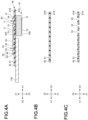
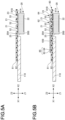
- FIGS. 3A to 3C , FIGS. 4A to 4C , FIGS. 5A and 5B , and FIGS. 6A and 6B are sectional views showing the method for manufacturing the semiconductor devices according to the first embodiment.
- a so-called multiplepiece manufacturing method will be described. That is, a part corresponding to a large number of semiconductor devices 1 is produced by batch and then divided into individual pieces to manufacture the semiconductor devices 1. Incidentally, for convenience of explanation, portions that will finally become constituent elements of each of the semiconductor devices 1 will be designated by the same reference signs as those for the final constituent elements.
- a large-sized insulating base member 41 having one face 41A and the other face 41B is prepared.
- the large-sized insulating base member 41 for example, a plurality of individual regions in each of which a semiconductor device 1 should be formed are consecutively provided in a matrix form.
- the individual regions are regions each of which will be finally cut into an individual piece along predetermined cutting lines to form the individual semiconductor device 1.
- the number of the individual regions contained in the large-sized insulating base member 41 is not limited particularly.
- An insulating adhesive layer 42 that covers the entire face 41A of the insulating base member 41 is provided on the face 41A.
- through holes 51, 53, and 54 are formed at required places in the insulating base member 41 and the adhesive layer 42 to penetrate through the insulating base member 41 and the adhesive layer 42 in a thickness direction.
- the through holes 51, 53 and 54 can be formed, for example, by a laser machining method using a CO 2 laser, a UV-YAG laser, etc. or by a punching method.
- the through holes 51 are formed on an X2 side of the through hole 54
- the through holes 53 are formed on an X2 side of the through holes 51.
- a semiconductor element 10 and a lead terminal 130 are adhesively bonded to the insulating base member 41 by the adhesive layer 42.
- alignment is performed to make one face 10A of the semiconductor element 10 face the face 41A of the insulating base member 41, so that electrodes 11 overlap with the through holes 51 and an electrode 13 overlaps with the through hole 54 in plan view.
- alignment is performed to make the lead terminal 130 overlap with the through holes 53 in plan view.
- a wiring layer 45 including a seed layer 43 and a metal layer 44 is formed on the other face 41B of the insulating base member 41.
- the wiring layer 45 can be formed, for example, by a semi-additive method.
- the seed layer 43 is formed to cover the entire other face 41B of the insulating base member 41 and entire inner faces of the through holes 51, 53 and 54.
- the seed layer 43 can be formed, for example, by a sputtering method or an electroless plating method.
- the seed layer 43 is formed by the sputtering method, first, titanium is deposited by sputtering to form a Ti layer to thereby cover the other face 41B of the insulating base member 41 and the inner faces of the through holes 51, 53, and 54. Then, copper is deposited on the Ti layer by sputtering to form a Cu layer.
- the seed layer 43 having a two-layer structure (the Ti layer/the Cu layer) can be formed.
- the seed layer 43 consisting of a Cu layer (one-layer structure) can be formed by an electroless copper plating method.
- a plating resist layer (not shown) is formed on the seed layer 43.
- the plating resist layer has opening portions provided in a portion where the wiring layer 45 should be formed, i.e. the portion where a wiring 61 and a wiring 63 should be formed.
- a metal layer 44 made of copper or the like is formed in the opening portions of the plating resist layer by an electrolytic plating method using the seed layer 43 as a plating power feed path. Then, the plating resist layer is removed.
- the seed layer 43 is removed by wet etching. In this manner, the wiring layer 45 including the seed layer 43 and the metal layer 44 can be formed.
- the wiring layer 45 has the wirings 61 and 63.
- a flexible wiring substrate 40 is constituted by the insulating base member 41, the adhesive layer 42, and the wiring layer 45.
- a large-sized insulating base member 81 having one face 81A and the other face 81B is prepared.
- the large-sized insulating base member 81 for example, a plurality of individual regions in each of which the semiconductor device 1 should be formed are consecutively provided in a matrix form.
- the individual regions are regions each of which will be finally cut into an individual piece along predetermined cutting lines to form the individual semiconductor device 1.
- the number of the individual regions contained in the large-sized insulating base member 81 is not limited particularly.
- An insulating adhesive layer 82 that covers the entire face 81A of the insulating base member 81 is provided on the face 81A.
- FIGS. 4B to 5B illustrate a state in which the large-sized insulating base member 81 is rotated 180° around the Y1-Y2 direction with respect to FIG. 1 .
- through holes 52 and 55 are formed at required places in the insulating base member 81 and the adhesive layer 82 to penetrate through the insulating base member 81 and the adhesive layer 82 in the thickness direction.
- the through holes 51 and 54 can be formed, for example, by a method the same as or similar to the through holes 52 and 55.
- the through holes 52 are formed on an X1 side of the through hole 55.
- a semiconductor element 20 and a lead terminal 110 are adhesively bonded to the insulating base member 81 by the adhesive layer 82.
- alignment is performed to make one face 20A of the semiconductor element 20 face the face 81A of the insulating base member 81, so that electrodes 21 overlap with the through holes 52 and an electrode 23 overlaps with the through hole 55 in the plan view.
- the lead terminal 110 is positioned on an X1 side of the semiconductor element 20.
- a wiring layer 85 including a seed layer 83 and a metal layer 84 is formed on the other face 81B of the insulating base member 81.
- the wiring layer 85 can be formed, for example, by a method the same as or similar to the wiring layer 45.
- the wiring layer 85 has wirings 62 and 64.
- a flexible wiring substrate 80 is constituted by the insulating base member 81, the adhesive layer 82 and the wiring layer 85.
- the flexible wiring substrate 80 is inverted vertically. Then, an electrically conductive adhesive layer 71 is provided on the lead terminal 110, an electrically conductive adhesive layer 72 is provided on a Z2-side face of the wiring 62 of the wiring layer 85, and an electrically conductive adhesive layer 73 is provided on a face 20B of the semiconductor element 20.
- the electrically conductive adhesive layers 71 to 73 are in an uncured state.
- an electrode 12 is bonded to the lead terminal 110 by the electrically conductive adhesive layer 71, and the lead terminal 130 is bonded to an electrode 22 by the electrically conductive adhesive layer 73. Moreover, a lead terminal 120 is bonded to the wiring 62 by the electrically conductive adhesive layer 72. During the bonding, the electrically conductive adhesive layers 71 to 73 are cured.
- the semiconductor device 1 according to the first embodiment can be manufactured.
- the semiconductor device 1 In the semiconductor device 1 according to the first embodiment, current flows from the P terminal toward the N terminal. Therefore, in the lead terminal 110, the current flows from the X1 side toward the X2 side, and in the lead terminal 120, the current flows from the X2 side toward the X1 side. Thus, inductance is generated between the lead terminal 110 and the lead terminal 120. Moreover, in the present embodiment, the distance between the lead terminal 110 and the lead terminal 120 is nearly comparable to the thickness of the flexible wiring substrate 80. Therefore, the distance between the lead terminal 110 and the lead terminal 120 becomes sufficiently small due to the thickness of the flexible wiring substrate 80. Accordingly, the inductance between the lead terminal 110 and the lead terminal 120 which are parallel reciprocating conducting lines can be reduced. Thus, it is possible to provide the semiconductor device 1 that can achieve high-speed switching operation.
- the wiring layer 45 can be formed on the other face 41B of the insulating base member 41 finely and with high accuracy by the semi-additive method, and the wiring layer 85 can be formed on the other face 81B of the insulating base member 81 finely and with high accuracy by the semi-additive method.
- the wiring layer 45 may be alternatively formed on the other face 41B of the insulating base member 41 by a subtractive method, and the wiring layer 85 may be alternatively formed on the other face 81B of the insulating base member 81 by a subtractive method.
- the semiconductor element 10 is adhesively bonded to the face 41A of the insulating base member 41 by the adhesive layer 42 so that the position of the semiconductor element 10 can be fixed to the insulating base member 41 and the wiring layer 45
- the semiconductor element 20 is adhesively bonded to the face 81A of the insulating base member 81 by the adhesive layer 82 so that the position of the semiconductor element 20 can be fixed to the insulating base member 81 and the wiring layer 85. Therefore, according to the present embodiment, it is possible to obtain excellent positional accuracy and connection reliability. Particularly, the semiconductor elements 10 and 20 can be aligned with high accuracy. Further, it is possible to secure high connection reliability between the semiconductor element 10 and the insulating base member 41, and it is possible to secure high connection reliability between the semiconductor element 20 and the insulating base member 81.
- a semiconductor device in which each of semiconductor elements is fixed to a metal foil (such as a copper foil) provided on the surface of an insulating substrate (such as a ceramic substrate) is manufactured as a reference example.
- solder reflow is performed to fix the semiconductor element, so that the semiconductor element may be considerably misaligned during this reflow process. Therefore, a relatively large margin is required for the placement of the semiconductor element in a design phase.
- the semiconductor element 10 is adhesively bonded to the insulating base member 41 in which the through holes 51 and 54 have been formed, and the wiring layer 45 is formed by the semi-additive method.
- the semiconductor element 20 is adhesively bonded to the insulating base member 81 in which the through holes 52 and 55 have been formed, and the wiring layer 85 is formed by the semi-additive method. Therefore, excellent positional accuracy and connection reliability can be obtained so that large margins as in the reference example are not required.
- the thickness T5 of the laminate structure body of the lead terminal 110 and the semiconductor element 10 and the thickness T6 of the laminate structure body of the semiconductor element 20 and the lead terminal 130 are equal to each other. Therefore, it is easy to perform alignment to bond the electrode 12 to the lead terminal 110 by the electrically conductive adhesive layer 71 and bond the lead terminal 130 to the electrode 22 by the electrically conductive adhesive layer 73.
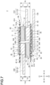
- FIG. 7 is a sectional view showing a semiconductor device according to the second embodiment.
- the semiconductor device 2 has a lead terminal 210 in place of the lead terminal 110, and has a lead terminal 230 in place of the lead terminal 130.
- Each of the lead terminals 210 and 230 is formed, for example, from a stepped lead frame.
- the lead terminal 210, 230 is an example of a wiring member.
- the lead terminal 210 has a junction portion 211 and an extension portion 212.
- the junction portion 211 is thicker than the extension portion 212.
- thickness of the extension portion 212 is equal to the thickness T3 of the lead terminal 110 in the first embodiment, and thickness T7 of the junction portion 211 is larger than the thickness T3.
- the junction portion 211 is bonded to an electrode 12 of a semiconductor element 10 by an electrically conductive adhesive layer 71, and adhesively bonded to one face 81A of an insulating base member 81 by an adhesive layer 82.
- the extension portion 212 extends from the junction portion 211 toward an X1 side.
- a Z1-side face of the junction portion 211 and a Z1-side face of the extension portion 212 are flush with each other.
- the junction portion 211 is an example of a first junction portion
- the extension portion 212 is an example of a first extension portion.
- the lead terminal 230 has a junction portion 231 and an extension portion 232.
- the junction portion 231 is thicker than the extension portion 232.
- thickness of the extension portion 232 is equal to the thickness T4 of the lead terminal 130 in the first embodiment, and thickness T8 of the junction portion 231 is larger than the thickness T4.
- the junction portion 231 is bonded to an electrode 22 of a semiconductor element 20 by an electrically conductive adhesive layer 73, and adhesively bonded to one face 41A of an insulating base member 41 by an adhesive layer 42.
- the extension portion 232 extends from the junction portion 231 toward an X2 side. For example, a Z2-side face of the junction portion 231 and a Z2-side face of the extension portion 232 are flush with each other.
- the junction portion 231 is an example of a second junction portion
- the extension portion 232 is an example of a second extension portion.
- the lead terminal 210 and a lead terminal 120 face each other in an X1-X2 direction, and are electrically connected to each other.
- the thickness T7 of the junction portion 211 and the thickness T8 of the junction portion 231 are equal to each other. Therefore, thickness T9 of a laminate structure body of the junction portion 211 and the semiconductor element 10 and thickness T10 of a laminate structure body of the semiconductor element 20 and the junction portion 231 are equal to each other.
- the remaining configuration is the same as or similar to that in the first embodiment.
- the lead terminals 210 and 230 are prepared in advance. Then, the lead terminal 210 is bonded to the semiconductor element 10 and the insulating base member 81 in place of the lead terminal 110, and the lead terminal 230 is bonded to the semiconductor element 20 and the insulating base member 41 in place of the lead terminal 130. In this manner, the semiconductor device 2 can be manufactured.
- a distance between the lead terminal 210 and the lead terminal 120 is defined by the sum of a difference in thickness between the junction portion 211 and the extension portion 212 and thickness of a flexible wiring substrate 80. Accordingly, the distance between the lead terminal 210 and the lead terminal 120 becomes sufficiently small. Thus, the inductance between the lead terminal 210 and the lead terminal 120 which are parallel reciprocating conducting lines can be reduced.
- the semiconductor device 2 that can achieve high-speed switching operation and it is possible to sufficiently dissipate heat generated from the semiconductor element 10 by the junction portion 211.
- the semiconductor device 2 having excellent positional accuracy and connection reliability can be provided in a manner the same as or similar to that in the first embodiment.
- the thickness T9 of the laminate structure body of the junction portion 211 and the semiconductor element 10 and the thickness T10 of the laminate structure body of the semiconductor element 20 and the junction portion 231 are equal to each other. Therefore, it is easy to perform alignment to bond the electrode 12 to the lead terminal 210 by the electrically conductive adhesive layer 71, and bond the junction portion 231 to the electrode 22 by the electrically conductive adhesive layer 73.
- junction portion 211 is thicker than the extension portion 212. Therefore, the lead terminal 210 is separated from the lead terminal 120 so as to make it easy to prevent a short circuit between the lead terminals 210 and 120.
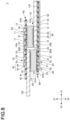
- FIG. 8 is a sectional view showing a semiconductor device according to the third embodiment.
- a flexible wiring substrate 80 extends along a Z2-side face of a lead terminal 110 toward an X1 side.
- a lead terminal 120 is absent.
- the lead terminal 110 and a wiring 62 face each other in an X1-X2 direction, and are electrically connected to each other.
- the remaining configuration are the same as or similar to that in the first embodiment.
- alignment has to be performed to make the lead terminal 110 and the wiring 62 extend in a common direction (toward the X1 side) as viewed from a semiconductor element 10.
- the wiring 62 of a wiring layer 85 exerts a function the same as or similar to the lead terminal 120.
- inductance is generated between the lead terminal 110 and the wiring 62.
- a distance between the lead terminal 110 and the wiring 62 becomes sufficiently small due to thickness of the flexible wiring substrate 80.
- the inductance between the lead terminal 110 and the wiring 62, which are parallel reciprocating conducting lines, can be reduced more than that in the first embodiment.
- the semiconductor device 3 having excellent positional accuracy and connection reliability can be provided in a manner the same as or similar to that in the first embodiment.
- a step required for bonding the lead terminal 120 can be omitted.
Landscapes
- Internal Circuitry In Semiconductor Integrated Circuit Devices (AREA)
- Semiconductor Integrated Circuits (AREA)
- Bipolar Integrated Circuits (AREA)
Abstract
Description
- The present disclosure relates to a semiconductor device.
- There has been known a semiconductor device in which each of semiconductor elements is attached to a film of a resin such as polyimide through an adhesive layer and a wiring layer is formed on a face of the resin film on an opposite side to the adhesive layer (e.g. see
JP-A-2016-046523 - On the other hand, further reduction of inductance generated in the semiconductor device is demanded to achieve high-speed switching operation of the semiconductor device.
- The present disclosure aims to provide a semiconductor device capable of reducing inductance.
- A certain embodiment provides a semiconductor device. The semiconductor device includes: a first semiconductor element including a first face and a second face opposite to the first face, wherein a first electrode is provided in the first face and a second electrode is provided in the second face; a second semiconductor element including a third face and a fourth face opposite to the third face, wherein a third electrode is provided in the third face and a fourth electrode is provided in the fourth face; a first insulating base member including a fifth face to which the first face of the first semiconductor element is adhesively bonded, and a sixth face opposite to the fifth face; a second insulating base member including a seventh face to which the third face of the second semiconductor element is adhesively bonded, and an eighth face opposite to the seventh face; a first wiring that penetrates through the first insulating base member to be electrically connected to the first electrode, and that is disposed on the sixth face of the first insulating base member; a second wiring that penetrates through the second insulating base member to be electrically connected to the third electrode, and that is disposed on the eighth face of the second insulating base member; a first wiring member that faces the second face of the first semiconductor element, and that is electrically connected to the second electrode; and a second wiring member that is provided on the second wiring to be electrically connected to the second wiring. The first wiring member is provided on the seventh face of the second insulating base member. The first wiring member and the second wiring member face each other and are electrically connected to each other. A current flows in a first direction in the first wiring member, and flows in a second direction opposite to the first direction in the second wiring member.
- A certain embodiment provides a semiconductor device. The semiconductor device includes: a first semiconductor element including a first face and a second face opposite to the first face, wherein a first electrode is provided in the first face and a second electrode is provided in the second face; a second semiconductor element including a third face and a fourth face opposite to the third face, wherein a third electrode is provided in the third face and a fourth electrode is provided in the fourth face; a first insulating base member including a fifth face to which the first face of the first semiconductor element is adhesively bonded, and a sixth face opposite side to the fifth face; a second insulating base member including a seventh face to which the third face of the second semiconductor element is adhesively bonded, and an eighth face opposite to the seventh face; a first wiring that penetrates through the first insulating base member to be electrically connected to the first electrode, and that is disposed on the sixth face of the first insulating base member; a second wiring that penetrates through the second insulating base member to be electrically connected to the third electrode, and that is disposed on the eighth face of the second insulating base member; and a first wiring member that faces the second face of the first semiconductor element, and that is electrically connected to the second electrode. The first wiring member is provided on the seventh face of the second insulating base member. The first wiring member and the second wiring face each other, and are electrically connected to each other. A current flows in a first direction in the first wiring member, and flows in a second direction opposite to the first direction in the second wiring.
-
-
FIG. 1 is a sectional view showing a semiconductor device according to a first embodiment; -
FIG. 2 is a circuit diagram showing the semiconductor device according to the first embodiment; -
FIGS. 3A to 3C are sectional views showing a method for manufacturing each semiconductor device according to the first embodiment (Part 1); -
FIGS. 4A to 4C are sectional views showing the method for manufacturing the semiconductor device according to the first embodiment (Part 2); -
FIGS. 5A and 5B are sectional views showing the method for manufacturing the semiconductor device according to the first embodiment (Part 3); -
FIGS. 6A and 6B are sectional views showing the method for manufacturing the semiconductor device according to the first embodiment (Part 4); -
FIG. 7 is a sectional view showing a semiconductor device according to a second embodiment; and -
FIG. 8 is a sectional view showing a semiconductor device according to a third embodiment. - Embodiments of the present disclosure will be described below specifically with reference to the accompanying drawings. Incidentally, in the description of the present disclosure and the drawings, constituent elements that have substantially the same functional configurations will be designated by the same reference signs correspondingly and respectively, and duplicated explanation about these constituent elements may be therefore omitted. In addition, in the present disclosure, an X1-X2 direction, a Y1-Y2 direction and a Z1-Z2 direction are set as directions mutually orthogonal to one another. A plane including the X1-X2 direction and the Y1-Y2 direction will be described as XY plane, a plane including the Y1-Y2 direction and the Z1-Z2 direction will be described as YZ plane, and a plane including the Z1-Z2 direction and the X1-X2 direction will be described as ZX plane. Incidentally, for convenience, the Z1-Z2 direction will be set as an up-down direction, with the Z1 side being an upper side and the Z2 side being a lower side. In addition, the term "plan view" will mean a view of an object from the Z1 side, and the term "planar shape" will mean the shape of the object viewed from the Z1 side. However, a semiconductor device can be used in a vertically inverted state, or can be disposed at any angle.
- First, a first embodiment will be described. The first embodiment relates to a semiconductor device.
- First, a sectional configuration of the semiconductor device according to the first embodiment will be described.
FIG. 1 is a sectional view showing the semiconductor device according to the first embodiment. - As shown in
FIG. 1 , thesemiconductor device 1 according to the first embodiment has asemiconductor element 10, asemiconductor element 20, aflexible wiring substrate 40, and aflexible wiring substrate 80. For example, a device using silicon (Si) or silicon carbide (SiC) can be used as each of thesemiconductor elements semiconductor element semiconductor element semiconductor element semiconductor element semiconductor element semiconductor element - The
semiconductor element 10 has oneface 10A, and theother face 10B located on an opposite side to theface 10A. In addition, thesemiconductor element 10 has abody portion 15,electrodes 11, anelectrode 12, and anelectrode 13. Theelectrodes 11 and theelectrode 13 are provided in theface 10A, and theelectrode 12 is provided in theother face 10B. For example, theelectrodes 11, theelectrode 12, and theelectrode 13 can be set as source electrodes, a drain electrode, and a gate electrode, respectively. - The
semiconductor element 20 has oneface 20A, and theother face 20B located on an opposite side to theface 20A. In addition, thesemiconductor element 20 has abody portion 25,electrodes 21, anelectrode 22, and anelectrode 23. Theelectrodes 21 and theelectrode 23 are provided in theface 20A, and theelectrode 22 is provided in theother face 20B. For example, theelectrodes 21, theelectrode 22, and theelectrode 23 can be set as source electrodes, a drain electrode, and a gate electrode, respectively. - For example, any of metals such as aluminum (Al) and copper (Cu), or an alloy containing at least one metal selected from these metals can be used as the material of the
electrodes 11, theelectrode 12, theelectrode 13, theelectrodes 21, theelectrode 22, and the electrode 23 (which may be hereinafter generically referred to as "electrodes"). Incidentally, if occasions demand, a surface treatment layer may be formed on each of surfaces of the electrodes. Examples of the surface treatment layer include a gold (Au) layer, a nickel (Ni) layer/Au layer (a metal layer in which the Ni layer and the Au layer are deposited in the named order), an Ni layer/palladium (Pd) layer/Au layer (a metal layer in which the Ni layer, the Pd layer, and the Au layer are deposited in the named order), etc. For example, a metal layer formed by an electroless plating method (an electroless plated metal layer) can be used as each of the Au layer, the Ni layer, and the Pd layer. In addition, the Au layer is a metal layer made of Au or an Au alloy, and the Ni layer is a metal layer made of Ni or an Ni alloy, and the Pd layer is a metal layer made of Pd or a Pd alloy. - The
flexible wiring substrate 40 has an insulatingbase member 41, an insulatingadhesive layer 42, and awiring layer 45. The insulatingbase member 41 has oneface 41A, and theother face 41B located on an opposite side to theface 41A. Theadhesive layer 42 is provided under theface 41A, and thewiring layer 45 is provided on theother face 41B. Thewiring layer 45 is deposited on theother face 41B. Thewiring layer 45 has aseed layer 43 and ametal layer 44. - The
flexible wiring substrate 80 has an insulatingbase member 81, an insulatingadhesive layer 82, and awiring layer 85. The insulatingbase member 81 has oneface 81A, and theother face 81B located on an opposite side to theface 81A. Theadhesive layer 82 is provided on theface 81A, and thewiring layer 85 is provided under theother face 81B. Thewiring layer 85 is deposited on theother face 81B. Thewiring layer 85 has aseed layer 83 and ametal layer 84. - For example, a resin film etc. can be used as each of the insulating
base members base member base member base member base member - The
semiconductor device 1 further has alead terminal 110, alead terminal 120, and alead terminal 130. Each of thelead terminals lead terminal - The
semiconductor element 10 and thelead terminal 130 are adhesively bonded to theface 41A of the insulatingbase member 41 by theadhesive layer 42. Theface 10A of thesemiconductor element 10 faces theface 41A of the insulatingbase member 41. Moreover, one face (Z1 side) of thelead terminal 130 faces theface 41A of the insulatingbase member 41. Throughholes 51 where theelectrodes 11 are exposed, throughholes 53 where thelead terminal 130 is exposed, and a throughhole 54 where theelectrode 13 is exposed are formed in the insulatingbase member 41 and theadhesive layer 42. - As the material of the
adhesive layer 42, for example, an adhesive agent such as an epoxy-based adhesive agent, a polyimide-based adhesive agent, or a silicone-based adhesive agent can be used. Thickness of theadhesive layer 42 can be, for example, set in a range of about 20 µm to 40 µm. - For example, the
electrodes 11 and the throughholes 51 are located on an X2 side of theelectrode 13 and the throughhole 54, and theelectrodes 21 and throughholes 52 are located on an X1 side of theelectrode 23 and a throughhole 55. Pairs of theelectrodes 11 and the throughholes 51 may be provided, and pairs of theelectrodes 21 and the throughholes 52 may be provided. - The
wiring layer 45 has awiring 61 connected to theelectrodes 11 through the throughholes 51, and awiring 63 connected to theelectrode 13 through the throughhole 54. Thewiring 61 is also connected to thelead terminal 130 through the through holes 53. - The
wiring 61 includes via wirings filled in the throughholes 51, via wirings filled in the throughholes 53, and a wiring pattern formed on theother face 41B of the insulatingbase member 41. Thewiring 63 includes a via wiring filled in the throughhole 54, and a wiring pattern formed on theother face 41B of the insulatingbase member 41. - The
seed layer 43 covers theother face 41B of the insulatingbase member 41 and inner faces of the throughholes seed layer 43 is formed to continuously cover theother face 41B of the insulatingbase member 41, the inner faces of the throughholes electrodes lead terminal 130 exposed at the bottoms of the throughholes seed layer 43. For example, a metal film with a two-layer structure in which a titanium (Ti) layer made of Ti and a copper (Cu) layer made of Cu are sequentially deposited on theother face 41B of the insulatingbase member 41 and the inner faces of the throughholes seed layer 43 formed by the sputtering method. In this case, thickness of the Ti layer can be, for example, set in a range of about 10 nm to 300 nm, and thickness of the Cu layer can be, for example, set in a range of about 100 nm to 1000 nm. Incidentally, the Ti layer functions as a close contact layer that improves close contactability of theseed layer 43 with the insulatingbase member 41 and the electrodes etc. In addition, the Ti layer also functions as a metal barrier layer that restrains copper from diffusing from the Cu layer etc. into the insulatingbase member 41 etc. In addition to the Ti, titanium nitride (TiN), tantalum nitride (TaN), tantalum (Ta), chrome (Cr), etc. can be used as the material of such a metal film functioning as the close contact layer and the metal barrier layer. - The
semiconductor element 20 and thelead terminal 110 are adhesively bonded to theface 81A of the insulatingbase member 81 by theadhesive layer 82. Theface 20A of thesemiconductor element 20 faces theface 81A of the insulatingbase member 81. The through holes 52 where theelectrodes 21 are exposed and the throughhole 55 where theelectrode 23 is exposed are formed in the insulatingbase member 81 and theadhesive layer 82. - For example, an adhesive agent such as an epoxy-based adhesive agent, a polyimide-based adhesive agent, or a silicone-based adhesive agent can be used as the material of the
adhesive layer 82. Thickness of theadhesive layer 82 can be, for example, set in a range of about 20 µm to 40 µm. - The
wiring layer 85 has awiring 62 connected to theelectrodes 21 through the throughholes 52, and awiring 64 connected to theelectrode 23 through the throughhole 55. - The
wiring 62 includes via wirings filled in the throughholes 52, and a wiring pattern formed on theother face 81B of the insulatingbase member 81. Thewiring 64 includes a via wiring filled in the throughhole 55, and a wiring pattern formed on theother face 81B of the insulatingbase member 81. - The
seed layer 83 covers theother face 81B of the insulatingbase member 81 and inner faces of the throughholes seed layer 83 is formed to continuously cover theother face 81B of the insulatingbase member 81, the inner faces of the throughholes holes seed layer 83. For example, a metal film with a two-layer structure in which a titanium (Ti) layer made of Ti and a copper (Cu) layer made of Cu are sequentially deposited on theother face 81B of the insulatingbase member 81 and the inner faces of the throughholes seed layer 83 formed by the sputtering method. In this case, thickness of the Ti layer can be, for example, set in a range of about 10 nm to 300 nm, and thickness of the Cu layer can be, for example, set in a range of about 100 nm to 1000 nm. Incidentally, the Ti layer functions as a close contact layer that improves close contactability of theseed layer 83 with the insulatingbase member 81 and the electrodes etc. In addition, the Ti layer also functions as a metal barrier layer that restrains copper from diffusing from the Cu layer etc. into the insulatingbase member 81 etc. In addition to the Ti, titanium nitride (TiN), tantalum nitride (TaN), tantalum (Ta), chrome (Cr), etc. can be used as the material of such a metal film functioning as the close contact layer and the metal barrier layer. - For example, copper or a copper alloy can be used as the material of the metal layers 44 and 84. For example, a metal layer formed by an electrolytic plating method (an electrolytic plated metal layer) can be used as each of the metal layers 44 and 84.
- One face (Z1 side) of the
lead terminal 110 is bonded to theelectrode 12 of thesemiconductor element 10 by an electrically conductiveadhesive layer 71. Moreover, the other face (Z2 side) of thelead terminal 110 is adhesively bonded to theadhesive layer 82. One face (Z1 side) of thelead terminal 120 is bonded to thewiring 62 of thewiring layer 45 by an electrically conductiveadhesive layer 72. One face (Z2 side) of thelead terminal 130 is bonded to theelectrode 22 of thesemiconductor element 20 by an electrically conductiveadhesive layer 73. Moreover, the other side (Z1 side) of thelead terminal 130 is adhesively bonded to theadhesive layer 42 to be electrically connected to thewiring 61. Each of the electrically conductiveadhesive layers 71 to 73 is, for example, a solder layer or a sintered metal layer. The electrically conductiveadhesive layer - The
semiconductor element 10 and thesemiconductor element 20 are arranged side by side in a horizontal direction, e.g., in the X1-X2 direction. Thesemiconductor element 20 is positioned on an X2 side of thesemiconductor element 10. - The
lead terminals semiconductor element 10. Accordingly, thesemiconductor element 20 is disposed on an opposite side of thesemiconductor element 10 to the direction in which thelead terminals semiconductor element 10. A distance between thelead terminals flexible wiring substrate 80. The distance between thelead terminals lead terminal 130 extends toward the X2 side, as viewed from thesemiconductor element 10. Thelead terminals - For example, thickness T1 of the
semiconductor element 10 and thickness T2 of thesemiconductor element 20 are equal to each other. Moreover, thickness T3 of thelead terminal 110 and thickness T4 of thelead terminal 130 are equal to each other. Therefore, thickness T5 of a laminate structure body of thelead terminal 110 and thesemiconductor element 10 and thickness T6 of a laminate structure body of thesemiconductor element 20 and thelead terminal 130 are equal to each other. Incidentally, the term "equal" in the present disclosure does not mean that the both are mathematically perfectly consistent with each other, but rather means that the both are in such a relationship that the both can be said to be "equal" to each other under socially accepted conventions. For example, one of the both is in a range of about 90% to 110% of the other. - The
electrode 12 of thesemiconductor element 10 is electrically connected to thelead terminal 110. Theelectrodes 21 of thesemiconductor element 20 are electrically connected to thelead terminal 120 through thewiring 62. Theelectrodes 11 of thesemiconductor element 10 and theelectrode 22 of thesemiconductor element 20 are electrically connected to thelead terminal 130 through thewiring 61. Moreover, a lead terminal (not shown) is also connected to thewiring 63 of thewiring layer 45, and this lead terminal is electrically connected to theelectrode 13 of thesemiconductor element 10. In the same manner or a similar manner, a lead terminal (not shown) is also connected to thewiring 64 of thewiring layer 85, and this lead terminal is electrically connected to theelectrode 23 of thesemiconductor element 20. - Here, a circuit configuration of the
semiconductor device 1 according to the first embodiment will be described.FIG. 2 is a circuit diagram showing the semiconductor device according to the first embodiment. - As shown in
FIG. 2 , theelectrode 12 of thesemiconductor element 10 is electrically connected to a P terminal through thelead terminal 110. Theelectrodes 21 of thesemiconductor element 20 are electrically connected to an N terminal through thelead terminal 120. Moreover, theelectrodes 11 of thesemiconductor element 10 and theelectrode 22 of thesemiconductor element 20 are electrically connected to an O terminal through thelead terminal 130. The P terminal is a positive input terminal, the N terminal is a negative input terminal, and the O terminal is an output terminal. Accordingly, a current flows in thelead terminal 110 in a reverse direction to a direction in which the current flows in thelead terminal 120. - Next, a method for manufacturing the semiconductor devices according to the first embodiment will be described.
FIGS. 3A to 3C ,FIGS. 4A to 4C ,FIGS. 5A and 5B , andFIGS. 6A and 6B are sectional views showing the method for manufacturing the semiconductor devices according to the first embodiment. In the following description, a so-called multiplepiece manufacturing method will be described. That is, a part corresponding to a large number ofsemiconductor devices 1 is produced by batch and then divided into individual pieces to manufacture thesemiconductor devices 1. Incidentally, for convenience of explanation, portions that will finally become constituent elements of each of thesemiconductor devices 1 will be designated by the same reference signs as those for the final constituent elements. - First, as shown in
FIG. 3A , a large-sizedinsulating base member 41 having oneface 41A and theother face 41B is prepared. In the large-sizedinsulating base member 41, for example, a plurality of individual regions in each of which asemiconductor device 1 should be formed are consecutively provided in a matrix form. Here, the individual regions are regions each of which will be finally cut into an individual piece along predetermined cutting lines to form theindividual semiconductor device 1. Incidentally, the number of the individual regions contained in the large-sizedinsulating base member 41 is not limited particularly. An insulatingadhesive layer 42 that covers theentire face 41A of the insulatingbase member 41 is provided on theface 41A. - Next, as shown in
FIG. 3B , throughholes base member 41 and theadhesive layer 42 to penetrate through the insulatingbase member 41 and theadhesive layer 42 in a thickness direction. The through holes 51, 53 and 54 can be formed, for example, by a laser machining method using a CO2 laser, a UV-YAG laser, etc. or by a punching method. For example, the throughholes 51 are formed on an X2 side of the throughhole 54, and the throughholes 53 are formed on an X2 side of the through holes 51. - Next, as shown in
FIG. 3C , asemiconductor element 10 and alead terminal 130 are adhesively bonded to the insulatingbase member 41 by theadhesive layer 42. On this occasion, alignment is performed to make oneface 10A of thesemiconductor element 10 face theface 41A of the insulatingbase member 41, so thatelectrodes 11 overlap with the throughholes 51 and anelectrode 13 overlaps with the throughhole 54 in plan view. In addition, alignment is performed to make thelead terminal 130 overlap with the throughholes 53 in plan view. - Next, as shown in
FIG. 4A , awiring layer 45 including aseed layer 43 and ametal layer 44 is formed on theother face 41B of the insulatingbase member 41. Thewiring layer 45 can be formed, for example, by a semi-additive method. - Specifically, the
seed layer 43 is formed to cover the entireother face 41B of the insulatingbase member 41 and entire inner faces of the throughholes seed layer 43 can be formed, for example, by a sputtering method or an electroless plating method. In the case where, for example, theseed layer 43 is formed by the sputtering method, first, titanium is deposited by sputtering to form a Ti layer to thereby cover theother face 41B of the insulatingbase member 41 and the inner faces of the throughholes seed layer 43 having a two-layer structure (the Ti layer/the Cu layer) can be formed. Moreover, in the case where theseed layer 43 is formed by the electroless plating method, for example, theseed layer 43 consisting of a Cu layer (one-layer structure) can be formed by an electroless copper plating method. - Next, a plating resist layer (not shown) is formed on the
seed layer 43. The plating resist layer has opening portions provided in a portion where thewiring layer 45 should be formed, i.e. the portion where awiring 61 and awiring 63 should be formed. Successively, ametal layer 44 made of copper or the like is formed in the opening portions of the plating resist layer by an electrolytic plating method using theseed layer 43 as a plating power feed path. Then, the plating resist layer is removed. Next, with themetal layer 44 used as a mask, theseed layer 43 is removed by wet etching. In this manner, thewiring layer 45 including theseed layer 43 and themetal layer 44 can be formed. Thewiring layer 45 has thewirings flexible wiring substrate 40 is constituted by the insulatingbase member 41, theadhesive layer 42, and thewiring layer 45. - Moreover, as shown in
FIG. 4B , a large-sizedinsulating base member 81 having oneface 81A and theother face 81B is prepared. In the large-sizedinsulating base member 81, for example, a plurality of individual regions in each of which thesemiconductor device 1 should be formed are consecutively provided in a matrix form. Here, the individual regions are regions each of which will be finally cut into an individual piece along predetermined cutting lines to form theindividual semiconductor device 1. Incidentally, the number of the individual regions contained in the large-sizedinsulating base member 81 is not limited particularly. An insulatingadhesive layer 82 that covers theentire face 81A of the insulatingbase member 81 is provided on theface 81A. Incidentally,FIGS. 4B to 5B illustrate a state in which the large-sizedinsulating base member 81 is rotated 180° around the Y1-Y2 direction with respect toFIG. 1 . - Next, as shown in
FIG. 4C , throughholes base member 81 and theadhesive layer 82 to penetrate through the insulatingbase member 81 and theadhesive layer 82 in the thickness direction. The through holes 51 and 54 can be formed, for example, by a method the same as or similar to the throughholes holes 52 are formed on an X1 side of the throughhole 55. - Next, as shown in
FIG. 5A , asemiconductor element 20 and alead terminal 110 are adhesively bonded to the insulatingbase member 81 by theadhesive layer 82. On this occasion, alignment is performed to make oneface 20A of thesemiconductor element 20 face theface 81A of the insulatingbase member 81, so thatelectrodes 21 overlap with the throughholes 52 and anelectrode 23 overlaps with the throughhole 55 in the plan view. In addition, thelead terminal 110 is positioned on an X1 side of thesemiconductor element 20. - Next, as shown in
FIG. 5B , awiring layer 85 including aseed layer 83 and ametal layer 84 is formed on theother face 81B of the insulatingbase member 81. Thewiring layer 85 can be formed, for example, by a method the same as or similar to thewiring layer 45. Thewiring layer 85 has wirings 62 and 64. Aflexible wiring substrate 80 is constituted by the insulatingbase member 81, theadhesive layer 82 and thewiring layer 85. - Next, as shown in
FIG. 6A , theflexible wiring substrate 80 is inverted vertically. Then, an electrically conductiveadhesive layer 71 is provided on thelead terminal 110, an electrically conductiveadhesive layer 72 is provided on a Z2-side face of thewiring 62 of thewiring layer 85, and an electrically conductiveadhesive layer 73 is provided on aface 20B of thesemiconductor element 20. The electrically conductiveadhesive layers 71 to 73 are in an uncured state. - Next, as shown in
FIG. 6B , anelectrode 12 is bonded to thelead terminal 110 by the electrically conductiveadhesive layer 71, and thelead terminal 130 is bonded to anelectrode 22 by the electrically conductiveadhesive layer 73. Moreover, alead terminal 120 is bonded to thewiring 62 by the electrically conductiveadhesive layer 72. During the bonding, the electrically conductiveadhesive layers 71 to 73 are cured. - In this manner, the
semiconductor device 1 according to the first embodiment can be manufactured. - In the
semiconductor device 1 according to the first embodiment, current flows from the P terminal toward the N terminal. Therefore, in thelead terminal 110, the current flows from the X1 side toward the X2 side, and in thelead terminal 120, the current flows from the X2 side toward the X1 side. Thus, inductance is generated between thelead terminal 110 and thelead terminal 120. Moreover, in the present embodiment, the distance between thelead terminal 110 and thelead terminal 120 is nearly comparable to the thickness of theflexible wiring substrate 80. Therefore, the distance between thelead terminal 110 and thelead terminal 120 becomes sufficiently small due to the thickness of theflexible wiring substrate 80. Accordingly, the inductance between thelead terminal 110 and thelead terminal 120 which are parallel reciprocating conducting lines can be reduced. Thus, it is possible to provide thesemiconductor device 1 that can achieve high-speed switching operation. - Moreover, the
wiring layer 45 can be formed on theother face 41B of the insulatingbase member 41 finely and with high accuracy by the semi-additive method, and thewiring layer 85 can be formed on theother face 81B of the insulatingbase member 81 finely and with high accuracy by the semi-additive method. Thewiring layer 45 may be alternatively formed on theother face 41B of the insulatingbase member 41 by a subtractive method, and thewiring layer 85 may be alternatively formed on theother face 81B of the insulatingbase member 81 by a subtractive method. Furthermore, thesemiconductor element 10 is adhesively bonded to theface 41A of the insulatingbase member 41 by theadhesive layer 42 so that the position of thesemiconductor element 10 can be fixed to the insulatingbase member 41 and thewiring layer 45, and thesemiconductor element 20 is adhesively bonded to theface 81A of the insulatingbase member 81 by theadhesive layer 82 so that the position of thesemiconductor element 20 can be fixed to the insulatingbase member 81 and thewiring layer 85. Therefore, according to the present embodiment, it is possible to obtain excellent positional accuracy and connection reliability. Particularly, thesemiconductor elements semiconductor element 10 and the insulatingbase member 41, and it is possible to secure high connection reliability between thesemiconductor element 20 and the insulatingbase member 81. - Assume that a semiconductor device (power module) in which each of semiconductor elements is fixed to a metal foil (such as a copper foil) provided on the surface of an insulating substrate (such as a ceramic substrate) is manufactured as a reference example. In manufacturing such a semiconductor device, solder reflow is performed to fix the semiconductor element, so that the semiconductor element may be considerably misaligned during this reflow process. Therefore, a relatively large margin is required for the placement of the semiconductor element in a design phase.
- On the other hand, in the present embodiment, the
semiconductor element 10 is adhesively bonded to the insulatingbase member 41 in which the throughholes wiring layer 45 is formed by the semi-additive method. In addition, thesemiconductor element 20 is adhesively bonded to the insulatingbase member 81 in which the throughholes wiring layer 85 is formed by the semi-additive method. Therefore, excellent positional accuracy and connection reliability can be obtained so that large margins as in the reference example are not required. - Furthermore, the thickness T5 of the laminate structure body of the
lead terminal 110 and thesemiconductor element 10 and the thickness T6 of the laminate structure body of thesemiconductor element 20 and thelead terminal 130 are equal to each other. Therefore, it is easy to perform alignment to bond theelectrode 12 to thelead terminal 110 by the electrically conductiveadhesive layer 71 and bond thelead terminal 130 to theelectrode 22 by the electrically conductiveadhesive layer 73. - Next, a second embodiment will be described.
FIG. 7 is a sectional view showing a semiconductor device according to the second embodiment. - As shown in
FIG. 7 , thesemiconductor device 2 according to the second embodiment has alead terminal 210 in place of thelead terminal 110, and has alead terminal 230 in place of thelead terminal 130. Each of thelead terminals lead terminal - The
lead terminal 210 has ajunction portion 211 and anextension portion 212. Thejunction portion 211 is thicker than theextension portion 212. For example, thickness of theextension portion 212 is equal to the thickness T3 of thelead terminal 110 in the first embodiment, and thickness T7 of thejunction portion 211 is larger than the thickness T3. Thejunction portion 211 is bonded to anelectrode 12 of asemiconductor element 10 by an electrically conductiveadhesive layer 71, and adhesively bonded to oneface 81A of an insulatingbase member 81 by anadhesive layer 82. Theextension portion 212 extends from thejunction portion 211 toward an X1 side. For example, a Z1-side face of thejunction portion 211 and a Z1-side face of theextension portion 212 are flush with each other. Thejunction portion 211 is an example of a first junction portion, and theextension portion 212 is an example of a first extension portion. - The
lead terminal 230 has ajunction portion 231 and anextension portion 232. Thejunction portion 231 is thicker than theextension portion 232. For example, thickness of theextension portion 232 is equal to the thickness T4 of thelead terminal 130 in the first embodiment, and thickness T8 of thejunction portion 231 is larger than the thickness T4. Thejunction portion 231 is bonded to anelectrode 22 of asemiconductor element 20 by an electrically conductiveadhesive layer 73, and adhesively bonded to oneface 41A of an insulatingbase member 41 by anadhesive layer 42. Theextension portion 232 extends from thejunction portion 231 toward an X2 side. For example, a Z2-side face of thejunction portion 231 and a Z2-side face of theextension portion 232 are flush with each other. Thejunction portion 231 is an example of a second junction portion, and theextension portion 232 is an example of a second extension portion. Thelead terminal 210 and alead terminal 120 face each other in an X1-X2 direction, and are electrically connected to each other. - For example, the thickness T7 of the
junction portion 211 and the thickness T8 of thejunction portion 231 are equal to each other. Therefore, thickness T9 of a laminate structure body of thejunction portion 211 and thesemiconductor element 10 and thickness T10 of a laminate structure body of thesemiconductor element 20 and thejunction portion 231 are equal to each other. - The remaining configuration is the same as or similar to that in the first embodiment.
- In order to manufacture the
semiconductor device 2 according to the second embodiment, thelead terminals lead terminal 210 is bonded to thesemiconductor element 10 and the insulatingbase member 81 in place of thelead terminal 110, and thelead terminal 230 is bonded to thesemiconductor element 20 and the insulatingbase member 41 in place of thelead terminal 130. In this manner, thesemiconductor device 2 can be manufactured. - In the
semiconductor device 2 according to the second embodiment, current also flows from a P terminal toward an N terminal. Therefore, in thelead terminal 210, the current flows from the X1 side toward the X2 side, and in thelead terminal 120, the current flows from the X2 side toward the X1 side. Thus, inductance is generated between thelead terminal 210 and thelead terminal 120. On the other hand, a distance between thelead terminal 210 and thelead terminal 120 is defined by the sum of a difference in thickness between thejunction portion 211 and theextension portion 212 and thickness of aflexible wiring substrate 80. Accordingly, the distance between thelead terminal 210 and thelead terminal 120 becomes sufficiently small. Thus, the inductance between thelead terminal 210 and thelead terminal 120 which are parallel reciprocating conducting lines can be reduced. Accordingly, it is possible to provide thesemiconductor device 2 that can achieve high-speed switching operation and it is possible to sufficiently dissipate heat generated from thesemiconductor element 10 by thejunction portion 211. Moreover, thesemiconductor device 2 having excellent positional accuracy and connection reliability can be provided in a manner the same as or similar to that in the first embodiment. - Furthermore, the thickness T9 of the laminate structure body of the
junction portion 211 and thesemiconductor element 10 and the thickness T10 of the laminate structure body of thesemiconductor element 20 and thejunction portion 231 are equal to each other. Therefore, it is easy to perform alignment to bond theelectrode 12 to thelead terminal 210 by the electrically conductiveadhesive layer 71, and bond thejunction portion 231 to theelectrode 22 by the electrically conductiveadhesive layer 73. - In addition, the
junction portion 211 is thicker than theextension portion 212. Therefore, thelead terminal 210 is separated from thelead terminal 120 so as to make it easy to prevent a short circuit between thelead terminals - Next, a third embodiment will be described.
FIG. 8 is a sectional view showing a semiconductor device according to the third embodiment. - As shown in
FIG. 8 , in the semiconductor device 3 according to the third embodiment, aflexible wiring substrate 80 extends along a Z2-side face of alead terminal 110 toward an X1 side. In addition, alead terminal 120 is absent. Thelead terminal 110 and awiring 62 face each other in an X1-X2 direction, and are electrically connected to each other. - The remaining configuration are the same as or similar to that in the first embodiment.
- For example, to adhesively bond the
lead terminal 110 to oneface 81A of an insulatingbase member 81 in order to manufacture the semiconductor device 3 according to the third embodiment, alignment has to be performed to make thelead terminal 110 and thewiring 62 extend in a common direction (toward the X1 side) as viewed from asemiconductor element 10. - In the semiconductor device 3 according to the third embodiment, the
wiring 62 of awiring layer 85 exerts a function the same as or similar to thelead terminal 120. Thus, inductance is generated between thelead terminal 110 and thewiring 62. On the other hand, a distance between thelead terminal 110 and thewiring 62 becomes sufficiently small due to thickness of theflexible wiring substrate 80. Thus, the inductance between thelead terminal 110 and thewiring 62, which are parallel reciprocating conducting lines, can be reduced more than that in the first embodiment. In addition, the semiconductor device 3 having excellent positional accuracy and connection reliability can be provided in a manner the same as or similar to that in the first embodiment. Furthermore, a step required for bonding thelead terminal 120 can be omitted. - Although the preferred embodiments etc. have been described above in detail, the present disclosure is not limited to the aforementioned embodiments etc., but various modifications and substitutions can be made on the aforementioned embodiments etc. without departing from the scope described in Claims.
Claims (15)
- A semiconductor device (1, 2) comprising:a first semiconductor element (10) comprising a first face (10A) and a second face (10B) opposite to the first face (10A), wherein a first electrode (11) is provided in the first face (10A) and a second electrode (12) is provided in the second face (10B);a second semiconductor element (20) comprising a third face (20A) and a fourth face (20B) opposite to the third face (20A), wherein a third electrode (21) is provided in the third face (20A) and a fourth electrode (22) is provided in the fourth face (20B);a first insulating base member (41) comprising a fifth face (41A) to which the first face (10A) of the first semiconductor element (10) is adhesively bonded, and a sixth face (41B) opposite to the fifth face (41A);a second insulating base member (81) comprising a seventh face (81A) to which the third face (20A) of the second semiconductor element (20) is adhesively bonded, and an eighth face (81B) opposite to the seventh face (81A);a first wiring (61) that penetrates through the first insulating base member (41) to be electrically connected to the first electrode (11), and that is disposed on the sixth face (41B) of the first insulating base member (41);a second wiring (62) that penetrates through the second insulating base member (81) to be electrically connected to the third electrode (21), and that is disposed on the eighth face (81B) of the second insulating base member (81);a first wiring member (110, 210) that faces the second face (10B) of the first semiconductor element (10), and that is electrically connected to the second electrode (12); anda second wiring member (120) that is provided on the second wiring (62) to be electrically connected to the second wiring (62),wherein:the first wiring member (110, 210) is provided on the seventh face (81A) of the second insulating base member (81);the first wiring member (110, 210) and the second wiring member (120) face each other and are electrically connected to each other; andthe semiconductor device is configured so that a current can flow in a first direction in the first wiring member (110, 210), and can flow in a second direction opposite to the first direction in the second wiring member (120).
- The semiconductor device according to Claim 1, wherein:
the first wiring member (110, 210) is electrically connected to the second wiring member (120) through the first semiconductor element (10), the first wiring (61), the second semiconductor element (20) and the second wiring (62). - The semiconductor device according to Claim 1 or 2, wherein
a distance between the first wiring member (110, 210) and the second wiring member (120) is defined by the sum of a thickness of the second insulating base member (81) and a thickness of the second wiring (62) disposed on the second insulating base member (81). - The semiconductor device according to any one of Claims 1 through 3, further comprising:a first electrically conductive adhesive layer (71) that bonds the first wiring member (110, 210) and the second electrode (12) to each other; anda second electrically conductive adhesive layer (72) that bonds the second wiring member (120) and the second wiring (62) to each other.
- The semiconductor device according to any one of Claims 1 through 4, wherein:the first wiring member (110, 210) comprises a first lead terminal; andthe second wiring member (120) comprises a second lead terminal.
- A semiconductor device (3) comprising:a first semiconductor element (10) comprising a first face (10A) and a second face (10B) opposite to the first face (10A), wherein a first electrode (11) is provided in the first face (10A) and a second electrode (12) is provided in the second face (10A);a second semiconductor element (20) comprising a third face (20A) and a fourth face (20B) opposite to the third face (20A), wherein a third electrode (21) is provided in the third face and a fourth electrode (22) is provided in the fourth face (20B);a first insulating base member (41) comprising a fifth face (41A) to which the first face (10A) of the first semiconductor element (10) is adhesively bonded, and a sixth face (41B) opposite side to the fifth face (41A);a second insulating base member (81) comprising a seventh face (81A) to which the third face (20A) of the second semiconductor element (20) is adhesively bonded, and an eighth face (81B) opposite to the seventh face (81A);a first wiring (61) that penetrates through the first insulating base member (41) to be electrically connected to the first electrode (11), and that is disposed on the sixth face (41B) of the first insulating base member (41);a second wiring (62) that penetrates through the second insulating base member (81) to be electrically connected to the third electrode (21), and that is disposed on the eighth face (81B) of the second insulating base member (81); anda first wiring member (110, 210) that faces the second face (10B) of the first semiconductor element (10), and that is electrically connected to the second electrode (12),wherein:the first wiring member (110, 210) is provided on the seventh face (81A) of the second insulating base member (81);the first wiring member (110, 210) and the second wiring (62) face each other, and are electrically connected to each other; andthe semiconductor device is configured so that a current can flow in a first direction in the first wiring member (110, 210), and can flow in a second direction opposite to the first direction in the second wiring (62).
- The semiconductor device according to Claim 6, wherein
the first wiring member (110, 210) is electrically connected to the second wiring (62) through the first semiconductor element (10), the first wiring (61) and the second semiconductor element (20). - The semiconductor device according to Claim 6 or 7, wherein
a distance between the first wiring member (110, 210) and the second wiring (62) is defined by a thickness of the second insulating base member (81). - The semiconductor device according to any one of Claims 1 through 8, further comprising:a third wiring member (130, 230) that is provided between the fourth face (20B) of the second semiconductor element (20) and the fifth face (41A) of the first insulating base member (41) to be electrically connected to the fourth electrode (22),wherein the first wiring (61) is electrically connected to the third wiring member (130, 230).
- The semiconductor device according to Claim 9, further comprising:
a third electrically conductive adhesive layer (73) that bonds the third wiring member (130, 230) and the fourth electrode (22) to each other. - The semiconductor device according to Claim 9 or 10, wherein
the third wiring member (130, 230) comprises a third lead terminal. - The semiconductor device according to any one of Claims 9 through 11, wherein:the second semiconductor element (20) and the first wiring member (110, 210) are disposed on the seventh face (81A) of the second insulating base member (81);the first semiconductor element (10) is disposed on the first wiring member (110, 210); andthe third wiring member (130, 230) is disposed on the second semiconductor element (20).
- The semiconductor device according to Claim 12, wherein
the sum of a thickness (T3) of the first wiring member (110) and a thickness (T1) of the first semiconductor element (10) is substantially equal to the sum of a thickness (T2) of the second semiconductor element (20) and a thickness (T4) of the third wiring member (130). - The semiconductor device according to any one of Claims 9 through 12, wherein;a thickness (T1) of the first semiconductor element (10) and a thickness (T2) of the second semiconductor element (20) are equal to each other;the first wiring member (210) comprises:a first junction portion (211) that is bonded to the first semiconductor element (10) and the second insulating base member (81) and that has a first thickness (T7); anda first extension portion (212) that extends from the first junction portion (211) and that has a second thickness smaller than the first thickness;the third wiring member (230) comprises:a second junction portion (231) that is bonded to the first insulating base member (41) and the second semiconductor element (20) and that has a third thickness (T8); anda second extension portion (232) that extends from the second junction portion (231) and that has a fourth thickness smaller than the third thickness; andthe first thickness is equal to the third thickness.
- The semiconductor device according to any one of Claims 1 through 14, wherein:the first semiconductor element (10) further comprises a fifth electrode (13) that is provided in the first face (10A);the second semiconductor element (20) further comprises a sixth electrode (23) that is provided in the third face (20A); andthe semiconductor device further comprises:a third wiring (63) that penetrates through the first insulating base member (41) to be electrically connected to the fifth electrode (13), and that is disposed on the sixth face (41B) of the first insulating base member; anda fourth wiring (64) that penetrates through the second insulating base member (81) to be electrically connected to the sixth electrode (23), and that is disposed on the eighth face (81B) of the second insulating base member.
Applications Claiming Priority (1)
| Application Number | Priority Date | Filing Date | Title |
|---|---|---|---|
| JP2021183971A JP7666780B2 (en) | 2021-11-11 | 2021-11-11 | Semiconductor Device |
Publications (1)
| Publication Number | Publication Date |
|---|---|
| EP4181188A1 true EP4181188A1 (en) | 2023-05-17 |
Family
ID=84370057
Family Applications (1)
| Application Number | Title | Priority Date | Filing Date |
|---|---|---|---|
| EP22206668.0A Pending EP4181188A1 (en) | 2021-11-11 | 2022-11-10 | Semiconductor device |
Country Status (4)
| Country | Link |
|---|---|
| US (1) | US20230145328A1 (en) |
| EP (1) | EP4181188A1 (en) |
| JP (1) | JP7666780B2 (en) |
| CN (1) | CN116110871A (en) |
Families Citing this family (1)
| Publication number | Priority date | Publication date | Assignee | Title |
|---|---|---|---|---|
| US20250140747A1 (en) * | 2023-10-31 | 2025-05-01 | Nanya Technology Corporation | Semiconductor package structure and method of manufacturing the same |
Citations (5)
| Publication number | Priority date | Publication date | Assignee | Title |
|---|---|---|---|---|
| US20090072384A1 (en) * | 2007-09-14 | 2009-03-19 | Phoenix Precision Technology Corporation | Packaging substrate having heat-dissipating structure |
| US20100221872A1 (en) * | 2003-08-26 | 2010-09-02 | Shafidul Islam | Reversible leadless package and methods of making and using same |
| US20140070396A1 (en) * | 2012-09-12 | 2014-03-13 | Shinko Electric Industries Co., Ltd. | Semiconductor package and manufacturing method |
| JP2016046523A (en) | 2014-08-21 | 2016-04-04 | ゼネラル・エレクトリック・カンパニイ | Electrical interconnect structure for embedded semiconductor device package and method of manufacturing the same |
| US20170207160A1 (en) * | 2016-01-19 | 2017-07-20 | General Electronic Company | Power electronics package and method of manufacturing thereof |
Family Cites Families (6)
| Publication number | Priority date | Publication date | Assignee | Title |
|---|---|---|---|---|
| US7829386B2 (en) | 2005-08-17 | 2010-11-09 | General Electric Company | Power semiconductor packaging method and structure |
| JP4564937B2 (en) | 2006-04-27 | 2010-10-20 | 日立オートモティブシステムズ株式会社 | Electric circuit device, electric circuit module, and power conversion device |
| JP2014050118A (en) | 2012-08-29 | 2014-03-17 | Hitachi Ltd | Electric circuit device and method for manufacturing electric circuit device |
| JP7088094B2 (en) | 2019-03-19 | 2022-06-21 | 株式会社デンソー | Semiconductor equipment |
| JP2021052055A (en) | 2019-09-24 | 2021-04-01 | 太陽誘電株式会社 | Component module and manufacturing method thereof |
| US20220384297A1 (en) | 2020-01-21 | 2022-12-01 | Rohm Co., Ltd. | Semiconductor device |
-
2021
- 2021-11-11 JP JP2021183971A patent/JP7666780B2/en active Active
-
2022
- 2022-11-10 EP EP22206668.0A patent/EP4181188A1/en active Pending
- 2022-11-10 US US17/984,496 patent/US20230145328A1/en active Pending
- 2022-11-11 CN CN202211411337.2A patent/CN116110871A/en active Pending
Patent Citations (5)
| Publication number | Priority date | Publication date | Assignee | Title |
|---|---|---|---|---|
| US20100221872A1 (en) * | 2003-08-26 | 2010-09-02 | Shafidul Islam | Reversible leadless package and methods of making and using same |
| US20090072384A1 (en) * | 2007-09-14 | 2009-03-19 | Phoenix Precision Technology Corporation | Packaging substrate having heat-dissipating structure |
| US20140070396A1 (en) * | 2012-09-12 | 2014-03-13 | Shinko Electric Industries Co., Ltd. | Semiconductor package and manufacturing method |
| JP2016046523A (en) | 2014-08-21 | 2016-04-04 | ゼネラル・エレクトリック・カンパニイ | Electrical interconnect structure for embedded semiconductor device package and method of manufacturing the same |
| US20170207160A1 (en) * | 2016-01-19 | 2017-07-20 | General Electronic Company | Power electronics package and method of manufacturing thereof |
Also Published As
| Publication number | Publication date |
|---|---|
| JP7666780B2 (en) | 2025-04-22 |
| US20230145328A1 (en) | 2023-05-11 |
| JP2023071300A (en) | 2023-05-23 |
| CN116110871A (en) | 2023-05-12 |
Similar Documents
| Publication | Publication Date | Title |
|---|---|---|
| KR100419352B1 (en) | Chip scale surface mount package for semiconductor device and process of fabricating the same | |
| US8030131B2 (en) | Semiconductor module | |
| US7816784B2 (en) | Power quad flat no-lead semiconductor die packages with isolated heat sink for high-voltage, high-power applications, systems using the same, and methods of making the same | |
| US8823175B2 (en) | Reliable area joints for power semiconductors | |
| US10192849B2 (en) | Semiconductor modules with semiconductor dies bonded to a metal foil | |
| KR20110084444A (en) | Flexible and stackable semiconductor die packages, systems using the same, and methods of manufacturing the same | |
| EP2402992B1 (en) | Method of fabricating an embedded chip package | |
| JP7416638B2 (en) | Semiconductor device and semiconductor device manufacturing method | |
| US11869863B2 (en) | Semiconductor device | |
| EP4181188A1 (en) | Semiconductor device | |
| US12506063B2 (en) | Semiconductor device including semiconductor elements, insulating base members, wirings, and wiring members | |
| EP4181192A1 (en) | Semiconductor device | |
| US12581962B2 (en) | Semiconductor device | |
| CN111613586A (en) | Electronic device and manufacturing method of electronic device | |
| EP1336993B1 (en) | Assembly structure for electronic power integrated circuit formed on a semiconductor die and corresponding manufacturing process | |
| US11869844B2 (en) | Semiconductor device | |
| JP7823307B2 (en) | Semiconductor Devices | |
| JP2020107685A (en) | Semiconductor module | |
| US20230092639A1 (en) | Semiconductor device and method of manufacturing semiconductor device | |
| WO2023058487A1 (en) | Electronic device | |
| JP2024042182A (en) | Semiconductor device and method for manufacturing semiconductor device | |
| CN118737847A (en) | Method for manufacturing semiconductor device, corresponding semiconductor device and mounting assembly | |
| JPH0336755A (en) | Lead frame for semiconductor devices |
Legal Events
| Date | Code | Title | Description |
|---|---|---|---|
| PUAI | Public reference made under article 153(3) epc to a published international application that has entered the european phase |
Free format text: ORIGINAL CODE: 0009012 |
|
| STAA | Information on the status of an ep patent application or granted ep patent |
Free format text: STATUS: THE APPLICATION HAS BEEN PUBLISHED |
|
| AK | Designated contracting states |
Kind code of ref document: A1 Designated state(s): AL AT BE BG CH CY CZ DE DK EE ES FI FR GB GR HR HU IE IS IT LI LT LU LV MC ME MK MT NL NO PL PT RO RS SE SI SK SM TR |
|
| STAA | Information on the status of an ep patent application or granted ep patent |
Free format text: STATUS: REQUEST FOR EXAMINATION WAS MADE |
|
| 17P | Request for examination filed |
Effective date: 20231108 |
|
| RBV | Designated contracting states (corrected) |
Designated state(s): AL AT BE BG CH CY CZ DE DK EE ES FI FR GB GR HR HU IE IS IT LI LT LU LV MC ME MK MT NL NO PL PT RO RS SE SI SK SM TR |