EP4178044A1 - Connector - Google Patents
Connector Download PDFInfo
- Publication number
- EP4178044A1 EP4178044A1 EP21832088.5A EP21832088A EP4178044A1 EP 4178044 A1 EP4178044 A1 EP 4178044A1 EP 21832088 A EP21832088 A EP 21832088A EP 4178044 A1 EP4178044 A1 EP 4178044A1
- Authority
- EP
- European Patent Office
- Prior art keywords
- shell
- raised
- housing
- connector
- contact
- Prior art date
- Legal status (The legal status is an assumption and is not a legal conclusion. Google has not performed a legal analysis and makes no representation as to the accuracy of the status listed.)
- Pending
Links
Images




Classifications
-
- H—ELECTRICITY
- H01—ELECTRIC ELEMENTS
- H01R—ELECTRICALLY-CONDUCTIVE CONNECTIONS; STRUCTURAL ASSOCIATIONS OF A PLURALITY OF MUTUALLY-INSULATED ELECTRICAL CONNECTING ELEMENTS; COUPLING DEVICES; CURRENT COLLECTORS
- H01R24/00—Two-part coupling devices, or either of their cooperating parts, characterised by their overall structure
- H01R24/38—Two-part coupling devices, or either of their cooperating parts, characterised by their overall structure having concentrically or coaxially arranged contacts
- H01R24/40—Two-part coupling devices, or either of their cooperating parts, characterised by their overall structure having concentrically or coaxially arranged contacts specially adapted for high frequency
-
- H—ELECTRICITY
- H01—ELECTRIC ELEMENTS
- H01R—ELECTRICALLY-CONDUCTIVE CONNECTIONS; STRUCTURAL ASSOCIATIONS OF A PLURALITY OF MUTUALLY-INSULATED ELECTRICAL CONNECTING ELEMENTS; COUPLING DEVICES; CURRENT COLLECTORS
- H01R12/00—Structural associations of a plurality of mutually-insulated electrical connecting elements, specially adapted for printed circuits, e.g. printed circuit boards [PCB], flat or ribbon cables, or like generally planar structures, e.g. terminal strips, terminal blocks; Coupling devices specially adapted for printed circuits, flat or ribbon cables, or like generally planar structures; Terminals specially adapted for contact with, or insertion into, printed circuits, flat or ribbon cables, or like generally planar structures
- H01R12/70—Coupling devices
- H01R12/71—Coupling devices for rigid printing circuits or like structures
- H01R12/712—Coupling devices for rigid printing circuits or like structures co-operating with the surface of the printed circuit or with a coupling device exclusively provided on the surface of the printed circuit
-
- H—ELECTRICITY
- H01—ELECTRIC ELEMENTS
- H01R—ELECTRICALLY-CONDUCTIVE CONNECTIONS; STRUCTURAL ASSOCIATIONS OF A PLURALITY OF MUTUALLY-INSULATED ELECTRICAL CONNECTING ELEMENTS; COUPLING DEVICES; CURRENT COLLECTORS
- H01R13/00—Details of coupling devices of the kinds covered by groups H01R12/70 or H01R24/00 - H01R33/00
- H01R13/40—Securing contact members in or to a base or case; Insulating of contact members
-
- H—ELECTRICITY
- H01—ELECTRIC ELEMENTS
- H01R—ELECTRICALLY-CONDUCTIVE CONNECTIONS; STRUCTURAL ASSOCIATIONS OF A PLURALITY OF MUTUALLY-INSULATED ELECTRICAL CONNECTING ELEMENTS; COUPLING DEVICES; CURRENT COLLECTORS
- H01R13/00—Details of coupling devices of the kinds covered by groups H01R12/70 or H01R24/00 - H01R33/00
- H01R13/46—Bases; Cases
- H01R13/502—Bases; Cases composed of different pieces
- H01R13/508—Bases; Cases composed of different pieces assembled by a separate clip or spring
-
- H—ELECTRICITY
- H01—ELECTRIC ELEMENTS
- H01R—ELECTRICALLY-CONDUCTIVE CONNECTIONS; STRUCTURAL ASSOCIATIONS OF A PLURALITY OF MUTUALLY-INSULATED ELECTRICAL CONNECTING ELEMENTS; COUPLING DEVICES; CURRENT COLLECTORS
- H01R13/00—Details of coupling devices of the kinds covered by groups H01R12/70 or H01R24/00 - H01R33/00
- H01R13/46—Bases; Cases
- H01R13/516—Means for holding or embracing insulating body, e.g. casing, hoods
-
- H—ELECTRICITY
- H01—ELECTRIC ELEMENTS
- H01R—ELECTRICALLY-CONDUCTIVE CONNECTIONS; STRUCTURAL ASSOCIATIONS OF A PLURALITY OF MUTUALLY-INSULATED ELECTRICAL CONNECTING ELEMENTS; COUPLING DEVICES; CURRENT COLLECTORS
- H01R13/00—Details of coupling devices of the kinds covered by groups H01R12/70 or H01R24/00 - H01R33/00
- H01R13/648—Protective earth or shield arrangements on coupling devices, e.g. anti-static shielding
- H01R13/658—High frequency shielding arrangements, e.g. against EMI [Electro-Magnetic Interference] or EMP [Electro-Magnetic Pulse]
- H01R13/6581—Shield structure
-
- H—ELECTRICITY
- H01—ELECTRIC ELEMENTS
- H01R—ELECTRICALLY-CONDUCTIVE CONNECTIONS; STRUCTURAL ASSOCIATIONS OF A PLURALITY OF MUTUALLY-INSULATED ELECTRICAL CONNECTING ELEMENTS; COUPLING DEVICES; CURRENT COLLECTORS
- H01R13/00—Details of coupling devices of the kinds covered by groups H01R12/70 or H01R24/00 - H01R33/00
- H01R13/648—Protective earth or shield arrangements on coupling devices, e.g. anti-static shielding
- H01R13/658—High frequency shielding arrangements, e.g. against EMI [Electro-Magnetic Interference] or EMP [Electro-Magnetic Pulse]
- H01R13/6591—Specific features or arrangements of connection of shield to conductive members
- H01R13/6594—Specific features or arrangements of connection of shield to conductive members the shield being mounted on a PCB and connected to conductive members
-
- H—ELECTRICITY
- H01—ELECTRIC ELEMENTS
- H01R—ELECTRICALLY-CONDUCTIVE CONNECTIONS; STRUCTURAL ASSOCIATIONS OF A PLURALITY OF MUTUALLY-INSULATED ELECTRICAL CONNECTING ELEMENTS; COUPLING DEVICES; CURRENT COLLECTORS
- H01R12/00—Structural associations of a plurality of mutually-insulated electrical connecting elements, specially adapted for printed circuits, e.g. printed circuit boards [PCB], flat or ribbon cables, or like generally planar structures, e.g. terminal strips, terminal blocks; Coupling devices specially adapted for printed circuits, flat or ribbon cables, or like generally planar structures; Terminals specially adapted for contact with, or insertion into, printed circuits, flat or ribbon cables, or like generally planar structures
- H01R12/70—Coupling devices
- H01R12/71—Coupling devices for rigid printing circuits or like structures
- H01R12/712—Coupling devices for rigid printing circuits or like structures co-operating with the surface of the printed circuit or with a coupling device exclusively provided on the surface of the printed circuit
- H01R12/716—Coupling device provided on the PCB
-
- H—ELECTRICITY
- H01—ELECTRIC ELEMENTS
- H01R—ELECTRICALLY-CONDUCTIVE CONNECTIONS; STRUCTURAL ASSOCIATIONS OF A PLURALITY OF MUTUALLY-INSULATED ELECTRICAL CONNECTING ELEMENTS; COUPLING DEVICES; CURRENT COLLECTORS
- H01R2103/00—Two poles
-
- H—ELECTRICITY
- H01—ELECTRIC ELEMENTS
- H01R—ELECTRICALLY-CONDUCTIVE CONNECTIONS; STRUCTURAL ASSOCIATIONS OF A PLURALITY OF MUTUALLY-INSULATED ELECTRICAL CONNECTING ELEMENTS; COUPLING DEVICES; CURRENT COLLECTORS
- H01R24/00—Two-part coupling devices, or either of their cooperating parts, characterised by their overall structure
- H01R24/38—Two-part coupling devices, or either of their cooperating parts, characterised by their overall structure having concentrically or coaxially arranged contacts
- H01R24/40—Two-part coupling devices, or either of their cooperating parts, characterised by their overall structure having concentrically or coaxially arranged contacts specially adapted for high frequency
- H01R24/50—Two-part coupling devices, or either of their cooperating parts, characterised by their overall structure having concentrically or coaxially arranged contacts specially adapted for high frequency mounted on a PCB [Printed Circuit Board]
Definitions
- the present invention relates to a connector suited for transmission of high frequency signals.
- Patent Literature 1 discloses an invention in which flat coaxial cable ends, where a plurality of coaxial cables are gathered, are collectively connected to a circuit ground and a frame ground by way of a common electrically conductive member.
- the invention of Patent Literature 1 aims to eliminate the occurrence of potential variation and occurrence of impedance discontinuity of the ground side wiring.
- the present invention aims to provide a connector having satisfactory transmission characteristics over a wide band of high frequency.
- a connector of the invention for achieving the purpose described above includes, a housing formed with an accommodation space having an opening on a front surface facing a mating connector side and a rear surface turning away from the mating connector; an outer shell that covers the housing including the rear surface of the housing; a contact that is accommodated in the accommodation space for conduction with the mating connector; and an inner shell that is positioned in the accommodation space and covers the contact; wherein a spring portion that elastically presses the inner shell forward is provided between a portion of the outer shell spread along the rear surface of the housing and the inner shell.
- the inner shell is considered to have a structure of being separated into a plurality of portions or being partially separated even if connected to one portion in terms of the necessity of positioning the contact on the inner side and covering the contact.
- the inner shell may be partially formed with a gap when pressing is not carried out or may be formed with a portion that is not sufficiently in contact.
- the spring portion is provided, and the inner shell is elastically pressed forward. Therefore, even with the inner shell having a structure in which the gap is formed when pressing is not carried out or a portion that is not sufficiently in contact is formed, the gap is filled or sufficient contact is obtained, and satisfactory transmission characteristics over a wide band of high frequency is realized.
- the inner shell preferably includes a front shell and a back shell separated from or partially coupled to each other, the front shell and the back shell covering the contact to sandwich the contact from front side and back side.
- the contact can be covered so as to be sandwiched from the front side and the back side.
- the spring portion is preferably a raised piece provided on the outer shell and raised obliquely forward, the raised piece being elastically bent by abutting on the inner shell.
- a raised piece that is provided on the inner shell and raised toward the back side, and that elastically bends by abutting on the outer shell may be provided.
- the inner shell can be elastically pressed forward.
- the spring portion can be configured with a simple structure by providing such a raised piece regardless of whether to provide the raised piece on the outer shell or on the inner shell.
- the contact includes a first extended portion extending in a front-back direction for conduction with the mating connector, and a second extended portion bent and extending downward where a circuit board is positioned from a back end of the first extended portion, and connected to the circuit substrate; and the raised piece is abutted on the inner shell at a position below the first extended portion in an up-down direction.
- the contact includes the first extended portion extending in the front-back direction and the second extended portion extending downward, and the inner shell also has a shape of covering the contact having a shape of extending downward. Therefore, the position of the center of gravity of the inner shell in the up-down direction is at a position below the first extended portion.
- the entire inner shell can be pressed forward in a balanced manner by abutting the raised piece at a position below the first extended portion in the up-down direction than by abutting the raised piece at a position the same height as or above the first extended portion.
- the raised piece is preferably raised at an angle of 45° with respect to the up-down direction.
- the raised piece is raised at an angle smaller than 45° with respect to the up-down direction.
- the raised piece abuts on the inner shell a height position where the second extended portion extending in the up-down direction exists in the contact.
- the raised piece approaches parallel to the second extended portion of the contact when raised at an angle smaller than 45° with respect to the up-down direction as compared with when raised at an angle of 45°. This contributes to further improvement of signal transmission characteristics by such much.
- the raised piece is raised at an angle larger than 45° with respect to the up-down direction.
- the raised piece can strongly press the inner shell when raised at an angle larger than 45° with respect to the up-down direction as compared with when raised at an angle of 45°. Therefore, the gap formed in the inner shell or insufficient contact are more reliably resolved by such much, and the inner shell can be more strongly integrated.
- an inner housing that is positioned in the accommodation space and supports the contact is further arranged; where the inner shell covers the contact with the inner housing in between.
- Fig. 1 is an isometric view of a connector according to one embodiment of the invention.
- the connector 1 is a connector in which the forward side indicated with an arrow F is directed toward a mating connector (not illustrated) to be mated with the mating connector. Furthermore, the connector 1 is mounted on a circuit board (not illustrated) positioned on the lower side indicated with an arrow Z and soldered to the circuit board.
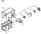
- Fig. 2 is an exploded isometric view of the connector, whose isometric view is illustrated in Fig. 1 .
- the connector 1 includes an outer housing 10 and an outer shell 20.
- the outer housing 10 is formed with an accommodation space 11.
- the accommodation space is formed with an opening on a front surface facing the mating connector side (facing the direction of the arrow F) and the rear surface turning away from the mating connector.
- the outer housing 10 corresponds to an example of a housing in the invention.
- the outer shell 20 is provided for shielding, and has a shape that covers an upper surface, left and right side surfaces, and a rear surface of the outer housing 10.
- the outer shell 20 is provided with a plurality of pin-shaped solder connecting portions 21 extending downward to be solder connected to the circuit board.
- the connector 1 includes a front shell 30, a front housing 40, a pin 50, a back housing 60, and a back shell 70.
- the pin 50 includes a first extended portion 51 extending in a front-back direction, and a second extended portion 52 bent and extended downward from a back end of the first extended portion 51.
- the first extended portion 51 comes into contact with and electrically conducts with a contact of a mating connector mated with the connector 1.
- the second extended portion 52 is solder-connected to a circuit board positioned below.
- the pin 50 corresponds to an example of a contact in the present invention.
- the front housing 40 and the back housing 60 support the pin 50 so as to sandwich the pin from the front side and the back side.
- a configuration combining the front housing 40 and the back housing 60 in the present embodiment corresponds to an example of an inner housing of the invention.
- the front shell 30 and the back shell 70 cover the pin 50 with the front housing 40 and the back housing 60 in between, and shields the pin 50.
- the front shell 30 is formed with six pin-shaped solder-connecting portions 31 extended downward and solder-connected to the circuit board.
- a configuration combining the front shell 30 and the back shell 70 corresponds to an example of an inner shell in the present invention.
- an assembly including the front shell 30, the front housing 40, the pin 50, the back housing 60, and the back shell 70 is referred to as a "sub-assembly 80".
- the sub-assembly 80 is charged into a main housing 10 from a rear surface side of the main housing 10.
- the sub-assembly 80 is inserted into the main housing 10, and the outer shell 20 is placed thereon to complete the connector 1 shown in Fig. 1 .
- Fig. 3 is an isometric view (A) showing a connector of the present embodiment in a direction in which the lower surface appears, and a rear view (B) of the connector of the present embodiment.
- Fig. 3(A) shows the second extended portion 52 of the pin 50, a plurality of solder-connecting portions 21 of the outer shell 20, and a plurality of (six) solder-connecting portions 31 of the front shell 30.
- the second extended portion 52 of only one pin 50 is for signal transmission.
- the other plurality of solder-connecting portions 21 of the outer shell 20 and the six solder-connecting portions 31 of the front shell 30 are for fixing the connector 1 to the circuit board, and are also for electrically grounding.
- eight portions, the two solder-connecting portions 21a of the plurality of solder-connecting portions 21 of the outer shell 20 and the six solder-connecting portions 31 of the front shell 30, are responsible for grounding.
- Such eight solder-connecting portions 21a, 31 are positioned to surround the second extended portion 52 of the pin 50.
- Fig. 3(B) shows a raised piece 22, which is a feature of the present embodiment.
- the raised piece 22 corresponds to an example of a spring portion and an example of a raised piece in the present invention.
- the raised piece 22 is provided in a region facing the rear surface of the outer housing 10 of the outer shell 20, and has a shape raised toward the front side, that is, in a direction of an arrow F shown in Figs. 1 and 2 .
- the operations of the raised piece 22 will be described below with reference to Fig. 4 .
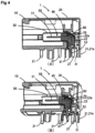
- Fig. 4 is a cross sectional view (A) and a cross sectional isometric view (B) taken along arrow A-A shown in Fig. 1 of the connector of the present embodiment.
- the raised piece 22 is raised at an angle of 45° with respect to the up-down direction in the present embodiment so as to collapse forward (direction of the arrow F shown in Figs. 1 and 2 ). Then, a distal end portion 22a of the raised piece 22 butts against the back shell 70.
- the raised piece 22 is shown so as to bite into the back shell 70, but this is to show the shape before deformation in design as is. In fact, the raised piece 22 butts against the back shell 70 and elastically deforms, and pushes the back shell 70 forward (direction of the arrow F). The back shell 70 is pushed by the raised piece 22, and abuts on the front shell 30 so as not to form even a slight gap with the front shell 30.
- the raised piece 22 abuts on the back shell 70 at a position below the first extended portion 51 extending in the front-back direction of the pin 50 in the up-down direction. Since the second extended portion 52 of the pin 50 is extended downward from the first extended portion 51, the back shell 70 is also greatly spread toward the lower side from the first extended portion 51, and the center of gravity of the back shell 70 is located on the lower side of the first extended portion 51. Therefore, the entire back shell 70 is pushed against the front shell 30 in a balanced manner by abutting the raised piece 22 on the back shell 70 at a position below the first extended portion 51.
- the spring portion in the present invention can be realized with a simple structure by forming such raised piece 22.
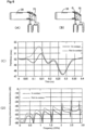
- Figs. 5 and 6 are views showing experiment results.
- FIG. 5 and 6 (A) is a view showing the front shell 30 and the back shell 70 in a state where the back shell 70 is butted on the front shell 30, and corresponds to one example of the invention.
- (B) is a view showing the front shell 30 and the back shell 70 in a state where the raised piece 22 (see Figs. 3 and 4 ) does not exist and a slight gap G is formed between the back shell 70 and the front shell 30.
- This (B) corresponds to a comparative example with respect to the present invention.
- Fig. 5(C) is a view showing a measurement result of an insertion loss (dB).
- the insertion loss (dB) is preferably closer to 0 dB, and an example in which the back shell 70 is in contact with the front shell 30 is more satisfactory in a high frequency region, in particular, 2.0 to 3.0 GHz as compared with a comparative example in which the back shell 70 is not in contact with the front shell 30.
- Fig. 5(D) is a view showing a measurement result of a voltage standing wave ratio (VSWR) on the circuit board side.
- VSWR voltage standing wave ratio
- the voltage standing wave ratio (VSWR) is preferably closer to 1, and the example of (A) is more satisfactory particularly in the high frequency region.
- Fig. 6(C) is a view showing a measurement result of an impedance on the circuit board side.
- the impedance is preferably always stable at 50 ohm, and the example of (A) is more satisfactory regarding the impedance as well.
- Fig. 6(D) is a view showing a measurement result of screening attenuation characteristics.
- the screening attenuation characteristics are preferably low, and the example of (A) is more satisfactory regarding the screening attenuation characteristics as well.
- the connector 1 of the present embodiment forms the raised piece 22 on the outer shell 20, and pushes the back shell 70 forward to push the back shell 70 against the front shell 0.
- the connector 1 of the present embodiment realizes satisfactory signal transmission characteristics as compared with a case where the raised piece 22 does not exist.
- the raised piece 22 is raised at an angle of 45° with respect to the up-down direction.
- the balance between the signal transmission characteristics and the ensuring of the pressing force of the back shell 70 against the front shell 30 is maintained.
- the raised piece 22 does not necessarily need to be raised at an angle of 45°.
- the raised piece 22 may be raised at an angle smaller than 45° with respect to the up-down direction.
- the raised piece 22 abuts on the back shell 70 at a position of the pin 50 where the second extended portion 52 extending in the up-down direction exists in the height direction.
- the raised piece 22 approaches to be parallel to the second extended portion 52 of the pin 50 as compared with a case where the raised piece is raised at an angle of 45°. Therefore, further improvement in the signal transmission characteristics by such much can be expected.
- the raised piece 22 may be raised at an angle larger than 45°.
- the spring force can be increased and the back shell 70 can be pushed stronger than when the raised piece 22 is raised at an angle of 45°. Therefore, the back shell 70 can be strongly pushed against the front shell 30 by such much, and the back shell 70 and the front shell 30 can be more strongly adhered.
- the raised piece 22 is provided on the outer shell 20.
- the raised piece 22 is a raised piece that is raised obliquely toward the front side and elastically bent by abutting on the back shell 70.
- a raised piece that is provided on the back shell 70 and raised toward the back side, and elastically bent by abutting on the outer shell 20 may be provided.
- the back shell 70 can be elastically pushed against the front shell 30.
- Fig. 7 is a view showing a modified example of the inner shell.
- a portion corresponding to the front shell and the back shell in the embodiment described above in the inner shell 90 is referred to as the front shell 30 and the back shell 70 as is.
- the inner shell 90 includes the front shell 30 and the back shell 70, which are partially coupled to each other.
- the inner shell 90 including the front shell 30 and the back shell 70, which are of a partially coupled structure the number of components are reduced as compared with when the front shell and the back shell are separated from each other, which is advantageous in terms of assembly and cost.
- the contact 50, as well as an inner housing including the front housing 40 and the back housing 60 that supports the contact 50 need to be charged inside the inner shell 90.
- the back shell 70 is set to an open posture as shown with a chain line in Fig. 7(A) with respect to the front shell 30.
- the back shell 70 is in a posture indicated with a solid line in Fig. 7(A) . If the back shell 70 remained in the posture indicated with the solid line, the gap G tends to be remained formed between the front shell 30 and the back shell 70.
- the back shell 70 is pressed forward by the raised piece 22 (see Figs. 3 and 4 ), so that the back shell 70 is pushed against the front shell 30.
- Fig. 7(B) shows the inner shell 90 in a pushed state. This pushing electrically integrates the front shell 30 and the back shell 70, and satisfactory signal transmission characteristics as shown in Figs. 5 and 6 can be obtained.
Landscapes
- Details Of Connecting Devices For Male And Female Coupling (AREA)
- Coupling Device And Connection With Printed Circuit (AREA)
Abstract
Description
- The present invention relates to a connector suited for transmission of high frequency signals.
- In the transmission of high frequency signals, reflection of the signal, or the like easily occurs, and how to realize satisfactory transmission characteristics becomes a concern. In particular, satisfactory transmission characteristics over a wide band of high frequency is required for the transmission of video signals.
-
Patent Literature 1 discloses an invention in which flat coaxial cable ends, where a plurality of coaxial cables are gathered, are collectively connected to a circuit ground and a frame ground by way of a common electrically conductive member. The invention ofPatent Literature 1 aims to eliminate the occurrence of potential variation and occurrence of impedance discontinuity of the ground side wiring. - PTL 1:
JP8-222325A - The present invention aims to provide a connector having satisfactory transmission characteristics over a wide band of high frequency.
- A connector of the invention for achieving the purpose described above includes, a housing formed with an accommodation space having an opening on a front surface facing a mating connector side and a rear surface turning away from the mating connector; an outer shell that covers the housing including the rear surface of the housing; a contact that is accommodated in the accommodation space for conduction with the mating connector; and an inner shell that is positioned in the accommodation space and covers the contact; wherein a spring portion that elastically presses the inner shell forward is provided between a portion of the outer shell spread along the rear surface of the housing and the inner shell.
- The inner shell is considered to have a structure of being separated into a plurality of portions or being partially separated even if connected to one portion in terms of the necessity of positioning the contact on the inner side and covering the contact. In this case, the inner shell may be partially formed with a gap when pressing is not carried out or may be formed with a portion that is not sufficiently in contact.
- In the connector of the invention, the spring portion is provided, and the inner shell is elastically pressed forward. Therefore, even with the inner shell having a structure in which the gap is formed when pressing is not carried out or a portion that is not sufficiently in contact is formed, the gap is filled or sufficient contact is obtained, and satisfactory transmission characteristics over a wide band of high frequency is realized.
- Thus, in the connector of the invention, the inner shell preferably includes a front shell and a back shell separated from or partially coupled to each other, the front shell and the back shell covering the contact to sandwich the contact from front side and back side.
- With the inner shell having the structure in which the inner shell is separated from or partially coupled to each other, the contact can be covered so as to be sandwiched from the front side and the back side.
- Furthermore, in the connector of the invention, the spring portion is preferably a raised piece provided on the outer shell and raised obliquely forward, the raised piece being elastically bent by abutting on the inner shell.
- As the spring portion, a raised piece that is provided on the inner shell and raised toward the back side, and that elastically bends by abutting on the outer shell may be provided. In the case of such configuration as well, the inner shell can be elastically pressed forward. However, it is considered advantages in terms of signal transmission characteristics to provide the raised piece on the outer shell than on the inner shell. Therefore, it is more preferable to arrange the raised piece on the outer shell.
- Furthermore, the spring portion can be configured with a simple structure by providing such a raised piece regardless of whether to provide the raised piece on the outer shell or on the inner shell.
- In addition, in the connector of the invention, preferably, the contact includes a first extended portion extending in a front-back direction for conduction with the mating connector, and a second extended portion bent and extending downward where a circuit board is positioned from a back end of the first extended portion, and connected to the circuit substrate; and the raised piece is abutted on the inner shell at a position below the first extended portion in an up-down direction.
- The contact includes the first extended portion extending in the front-back direction and the second extended portion extending downward, and the inner shell also has a shape of covering the contact having a shape of extending downward. Therefore, the position of the center of gravity of the inner shell in the up-down direction is at a position below the first extended portion. Thus, the entire inner shell can be pressed forward in a balanced manner by abutting the raised piece at a position below the first extended portion in the up-down direction than by abutting the raised piece at a position the same height as or above the first extended portion.
- Here, the raised piece is preferably raised at an angle of 45° with respect to the up-down direction.
- In this case, balance between the satisfactory signal transmission characteristics and the ensuring of sufficient pressing force on the inner shell is maintained.
- Alternatively, in a preferred aspect, the raised piece is raised at an angle smaller than 45° with respect to the up-down direction.
- The raised piece abuts on the inner shell a height position where the second extended portion extending in the up-down direction exists in the contact. The raised piece approaches parallel to the second extended portion of the contact when raised at an angle smaller than 45° with respect to the up-down direction as compared with when raised at an angle of 45°. This contributes to further improvement of signal transmission characteristics by such much.
- Alternatively, in a preferred aspect, the raised piece is raised at an angle larger than 45° with respect to the up-down direction.
- The raised piece can strongly press the inner shell when raised at an angle larger than 45° with respect to the up-down direction as compared with when raised at an angle of 45°. Therefore, the gap formed in the inner shell or insufficient contact are more reliably resolved by such much, and the inner shell can be more strongly integrated.
- Furthermore, in the connector of the invention, preferably, an inner housing that is positioned in the accommodation space and supports the contact is further arranged; where the inner shell covers the contact with the inner housing in between.
- With the arrangement of the inner housing, the positional displacement and the like of the contact are less likely to occur, and a stronger connector is realized.
-
-
Figure 1 is an isometric view of a connector according to one embodiment of the invention. -
Figure 2 is an exploded isometric view of the connector whose isometric view is shown inFigure 1 . -
Figure 3 is an isometric view (A) showing the connector of the present embodiment in a direction in which a lower surface appears, and a rear view (B) of the connector of the present embodiment. -
Figure 4 is a cross sectional view (A) and a cross sectional isometric view (B) taken along an arrow A-A shown inFig. 1 . -
Figure 5 is a view showing experiment results. -
Figure 6 is a view showing experiment results. -
Figure 7 is a view showing a modified example of an inner shell. -
Fig. 1 is an isometric view of a connector according to one embodiment of the invention. - The
connector 1 is a connector in which the forward side indicated with an arrow F is directed toward a mating connector (not illustrated) to be mated with the mating connector. Furthermore, theconnector 1 is mounted on a circuit board (not illustrated) positioned on the lower side indicated with an arrow Z and soldered to the circuit board. -
Fig. 2 is an exploded isometric view of the connector, whose isometric view is illustrated inFig. 1 . - The
connector 1 includes anouter housing 10 and anouter shell 20. - The
outer housing 10 is formed with anaccommodation space 11. The accommodation space is formed with an opening on a front surface facing the mating connector side (facing the direction of the arrow F) and the rear surface turning away from the mating connector. Theouter housing 10 corresponds to an example of a housing in the invention. - In addition, the
outer shell 20 is provided for shielding, and has a shape that covers an upper surface, left and right side surfaces, and a rear surface of theouter housing 10. Theouter shell 20 is provided with a plurality of pin-shapedsolder connecting portions 21 extending downward to be solder connected to the circuit board. - Furthermore, the
connector 1 includes afront shell 30, afront housing 40, apin 50, aback housing 60, and aback shell 70. - The
pin 50 includes a firstextended portion 51 extending in a front-back direction, and a secondextended portion 52 bent and extended downward from a back end of the firstextended portion 51. The firstextended portion 51 comes into contact with and electrically conducts with a contact of a mating connector mated with theconnector 1. The secondextended portion 52 is solder-connected to a circuit board positioned below. Thepin 50 corresponds to an example of a contact in the present invention. - The
front housing 40 and theback housing 60 support thepin 50 so as to sandwich the pin from the front side and the back side. A configuration combining thefront housing 40 and theback housing 60 in the present embodiment corresponds to an example of an inner housing of the invention. - Furthermore, the
front shell 30 and theback shell 70 cover thepin 50 with thefront housing 40 and theback housing 60 in between, and shields thepin 50. Thefront shell 30 is formed with six pin-shaped solder-connectingportions 31 extended downward and solder-connected to the circuit board. In the present embodiment, a configuration combining thefront shell 30 and theback shell 70 corresponds to an example of an inner shell in the present invention. - Here, an assembly including the
front shell 30, thefront housing 40, thepin 50, theback housing 60, and theback shell 70 is referred to as a "sub-assembly 80". The sub-assembly 80 is charged into amain housing 10 from a rear surface side of themain housing 10. The sub-assembly 80 is inserted into themain housing 10, and theouter shell 20 is placed thereon to complete theconnector 1 shown inFig. 1 . -
Fig. 3 is an isometric view (A) showing a connector of the present embodiment in a direction in which the lower surface appears, and a rear view (B) of the connector of the present embodiment. -
Fig. 3(A) shows the secondextended portion 52 of thepin 50, a plurality of solder-connectingportions 21 of theouter shell 20, and a plurality of (six) solder-connectingportions 31 of thefront shell 30. Among them, the secondextended portion 52 of only onepin 50 is for signal transmission. The other plurality of solder-connectingportions 21 of theouter shell 20 and the six solder-connectingportions 31 of thefront shell 30 are for fixing theconnector 1 to the circuit board, and are also for electrically grounding. In particular, eight portions, the two solder-connecting portions 21a of the plurality of solder-connectingportions 21 of theouter shell 20 and the six solder-connectingportions 31 of thefront shell 30, are responsible for grounding. Such eight solder-connectingportions 21a, 31 are positioned to surround the secondextended portion 52 of thepin 50. - Furthermore,
Fig. 3(B) shows a raisedpiece 22, which is a feature of the present embodiment. The raisedpiece 22 corresponds to an example of a spring portion and an example of a raised piece in the present invention. The raisedpiece 22 is provided in a region facing the rear surface of theouter housing 10 of theouter shell 20, and has a shape raised toward the front side, that is, in a direction of an arrow F shown inFigs. 1 and2 . The operations of the raisedpiece 22 will be described below with reference toFig. 4 . -
Fig. 4 is a cross sectional view (A) and a cross sectional isometric view (B) taken along arrow A-A shown inFig. 1 of the connector of the present embodiment. - The raised
piece 22 is raised at an angle of 45° with respect to the up-down direction in the present embodiment so as to collapse forward (direction of the arrow F shown inFigs. 1 and2 ). Then, adistal end portion 22a of the raisedpiece 22 butts against theback shell 70. InFig. 4 , the raisedpiece 22 is shown so as to bite into theback shell 70, but this is to show the shape before deformation in design as is. In fact, the raisedpiece 22 butts against theback shell 70 and elastically deforms, and pushes theback shell 70 forward (direction of the arrow F). Theback shell 70 is pushed by the raisedpiece 22, and abuts on thefront shell 30 so as not to form even a slight gap with thefront shell 30. - Here, the raised
piece 22 abuts on theback shell 70 at a position below the firstextended portion 51 extending in the front-back direction of thepin 50 in the up-down direction. Since the secondextended portion 52 of thepin 50 is extended downward from the firstextended portion 51, theback shell 70 is also greatly spread toward the lower side from the firstextended portion 51, and the center of gravity of theback shell 70 is located on the lower side of the firstextended portion 51. Therefore, theentire back shell 70 is pushed against thefront shell 30 in a balanced manner by abutting the raisedpiece 22 on theback shell 70 at a position below the firstextended portion 51. - In the present embodiment, the spring portion in the present invention can be realized with a simple structure by forming such raised
piece 22. -
Figs. 5 and6 are views showing experiment results. - In both
Figs. 5 and6, (A) is a view showing thefront shell 30 and theback shell 70 in a state where theback shell 70 is butted on thefront shell 30, and corresponds to one example of the invention. In bothFigs. 5 and6, (B) is a view showing thefront shell 30 and theback shell 70 in a state where the raised piece 22 (seeFigs. 3 and4 ) does not exist and a slight gap G is formed between theback shell 70 and thefront shell 30. This (B) corresponds to a comparative example with respect to the present invention. -
Fig. 5(C) is a view showing a measurement result of an insertion loss (dB). - The insertion loss (dB) is preferably closer to 0 dB, and an example in which the
back shell 70 is in contact with thefront shell 30 is more satisfactory in a high frequency region, in particular, 2.0 to 3.0 GHz as compared with a comparative example in which theback shell 70 is not in contact with thefront shell 30. - Furthermore,
Fig. 5(D) is a view showing a measurement result of a voltage standing wave ratio (VSWR) on the circuit board side. - The voltage standing wave ratio (VSWR) is preferably closer to 1, and the example of (A) is more satisfactory particularly in the high frequency region.
- Furthermore,
Fig. 6(C) is a view showing a measurement result of an impedance on the circuit board side. - The impedance is preferably always stable at 50 ohm, and the example of (A) is more satisfactory regarding the impedance as well.
- In addition,
Fig. 6(D) is a view showing a measurement result of screening attenuation characteristics. - The screening attenuation characteristics are preferably low, and the example of (A) is more satisfactory regarding the screening attenuation characteristics as well.
- Thus, the
connector 1 of the present embodiment forms the raisedpiece 22 on theouter shell 20, and pushes theback shell 70 forward to push theback shell 70 against thefront shell 0. Thus, theconnector 1 of the present embodiment realizes satisfactory signal transmission characteristics as compared with a case where the raisedpiece 22 does not exist. - In the present embodiment, the raised
piece 22 is raised at an angle of 45° with respect to the up-down direction. Thus, in the present embodiment, the balance between the signal transmission characteristics and the ensuring of the pressing force of theback shell 70 against thefront shell 30 is maintained. - However, the raised
piece 22 does not necessarily need to be raised at an angle of 45°. For example, the raisedpiece 22 may be raised at an angle smaller than 45° with respect to the up-down direction. The raisedpiece 22 abuts on theback shell 70 at a position of thepin 50 where the secondextended portion 52 extending in the up-down direction exists in the height direction. When raised at an angle smaller than 45°, the raisedpiece 22 approaches to be parallel to the secondextended portion 52 of thepin 50 as compared with a case where the raised piece is raised at an angle of 45°. Therefore, further improvement in the signal transmission characteristics by such much can be expected. - Alternatively, the raised
piece 22 may be raised at an angle larger than 45°. In this case, the spring force can be increased and theback shell 70 can be pushed stronger than when the raisedpiece 22 is raised at an angle of 45°. Therefore, theback shell 70 can be strongly pushed against thefront shell 30 by such much, and theback shell 70 and thefront shell 30 can be more strongly adhered. - Furthermore, in the present embodiment, the raised
piece 22 is provided on theouter shell 20. The raisedpiece 22 is a raised piece that is raised obliquely toward the front side and elastically bent by abutting on theback shell 70. However, in place of the raisedpiece 22, a raised piece that is provided on theback shell 70 and raised toward the back side, and elastically bent by abutting on theouter shell 20 may be provided. In the case of such a configuration as well, theback shell 70 can be elastically pushed against thefront shell 30. -
Fig. 7 is a view showing a modified example of the inner shell. Here, for the sake of easy understanding, a portion corresponding to the front shell and the back shell in the embodiment described above in theinner shell 90 is referred to as thefront shell 30 and theback shell 70 as is. - Even when the
inner shell 90 having the structure shown inFig. 7 is adopted, the structure of each portion other than theinner shell 90 follows those in the embodiment described above. - The
inner shell 90 includes thefront shell 30 and theback shell 70, which are partially coupled to each other. Thus, with theinner shell 90 including thefront shell 30 and theback shell 70, which are of a partially coupled structure, the number of components are reduced as compared with when the front shell and the back shell are separated from each other, which is advantageous in terms of assembly and cost. - The
contact 50, as well as an inner housing including thefront housing 40 and theback housing 60 that supports thecontact 50 need to be charged inside theinner shell 90. Thus, at the time point of charging, theback shell 70 is set to an open posture as shown with a chain line inFig. 7(A) with respect to thefront shell 30. After thecontact 50 and the inner housing (front housing 40 and back housing 60) are charged, theback shell 70 is in a posture indicated with a solid line inFig. 7(A) . If theback shell 70 remained in the posture indicated with the solid line, the gap G tends to be remained formed between thefront shell 30 and theback shell 70. - The
back shell 70 is pressed forward by the raised piece 22 (seeFigs. 3 and4 ), so that theback shell 70 is pushed against thefront shell 30.Fig. 7(B) shows theinner shell 90 in a pushed state. This pushing electrically integrates thefront shell 30 and theback shell 70, and satisfactory signal transmission characteristics as shown inFigs. 5 and6 can be obtained. -
- 1
- connector
- 10
- outer housing
- 11
- accommodation space
- 20
- outer shell
- 21, 21a
- solder-connecting portion
- 22
- raised piece
- 22a
- distal end portion of raised piece
- 30
- front shell
- 31
- solder-connecting portion
- 40
- front housing
- 50
- pin
- 51
- first extended portion
- 52
- second extended portion
- 60
- back housing
- 70
- back shell
- 80
- sub-assembly
- 90
- inner shell
Claims (8)
- A connector comprising:a housing formed with an accommodation space having an opening on a front surface facing a mating connector side and a rear surface turning away from the mating connector;an outer shell that covers the housing including the rear surface of the housing;a contact that is accommodated in the accommodation space for conduction with the mating connector; andan inner shell that is positioned in the accommodation space and covers the contact; whereina spring portion that elastically presses the inner shell forward is provided between a portion of the outer shell spread along the rear surface of the housing and the inner shell.
- The connector according to claim 1, wherein the inner shell includes a front shell and a back shell separated from or partially coupled to each other, the front shell and the back shell covering the contact to sandwich the contact from front side and back side.
- The connector according to claim 1 or 2, wherein the spring portion is a raised piece provided on the outer shell and raised obliquely forward, the raised piece being elastically bent by abutting on with the inner shell.
- The connector according to claim 3, whereinthe contact includes a first extended portion extending in a front-back direction for conduction with the mating connector, and a second extended portion bent and extending downward where a circuit board is positioned from a back end of the first extended portion, and connected to the circuit substrate; andthe raised piece abuts on the back shell at a position below the first extended portion in an up-down direction.
- The connector according to claim 4, wherein the raised piece is raised at an angle of 45° with respect to the up-down direction.
- The connector according to claim 4, wherein the raised piece is raised at an angle smaller than 45° with respect to the up-down direction.
- The connector according to claim 4, wherein the raised piece is raised at an angle larger than 45° with respect to the up-down direction.
- The connector according to any one of claims 1 to 7, further comprisingan inner housing that is positioned in the accommodation space and supports the contact; whereinthe inner shell covers the contact with the inner housing in between.
Applications Claiming Priority (2)
| Application Number | Priority Date | Filing Date | Title |
|---|---|---|---|
| JP2020115360A JP7479967B2 (en) | 2020-07-03 | 2020-07-03 | connector |
| PCT/JP2021/023259 WO2022004438A1 (en) | 2020-07-03 | 2021-06-18 | Connector |
Publications (2)
| Publication Number | Publication Date |
|---|---|
| EP4178044A1 true EP4178044A1 (en) | 2023-05-10 |
| EP4178044A4 EP4178044A4 (en) | 2024-07-31 |
Family
ID=79316155
Family Applications (1)
| Application Number | Title | Priority Date | Filing Date |
|---|---|---|---|
| EP21832088.5A Pending EP4178044A4 (en) | 2020-07-03 | 2021-06-18 | CONNECTOR |
Country Status (6)
| Country | Link |
|---|---|
| US (1) | US20230142379A1 (en) |
| EP (1) | EP4178044A4 (en) |
| JP (1) | JP7479967B2 (en) |
| KR (1) | KR20230028559A (en) |
| CN (1) | CN115735304B (en) |
| WO (1) | WO2022004438A1 (en) |
Families Citing this family (1)
| Publication number | Priority date | Publication date | Assignee | Title |
|---|---|---|---|---|
| US12586959B2 (en) * | 2023-02-07 | 2026-03-24 | Te Connectivity Solutions Gmbh | Angled connector |
Family Cites Families (8)
| Publication number | Priority date | Publication date | Assignee | Title |
|---|---|---|---|---|
| JPH08222325A (en) | 1995-02-13 | 1996-08-30 | Fujitsu Ltd | Connection method of flat coaxial cable to printed wiring board |
| JP5114275B2 (en) | 2007-07-18 | 2013-01-09 | 矢崎総業株式会社 | Shield connector structure |
| JP5836715B2 (en) * | 2011-09-07 | 2015-12-24 | 矢崎総業株式会社 | Shield connector |
| JP6422815B2 (en) | 2015-04-21 | 2018-11-14 | 日本航空電子工業株式会社 | connector |
| JP2017045604A (en) * | 2015-08-26 | 2017-03-02 | タイコエレクトロニクスジャパン合同会社 | Shield connector |
| JP6996445B2 (en) | 2018-07-20 | 2022-01-17 | 株式会社オートネットワーク技術研究所 | Shielded connector and outer conductor terminal |
| JP2020043024A (en) * | 2018-09-13 | 2020-03-19 | 矢崎総業株式会社 | Board connector |
| JP7398223B2 (en) | 2019-08-27 | 2023-12-14 | 矢崎総業株式会社 | Board-mounted connectors and boards with connectors |
-
2020
- 2020-07-03 JP JP2020115360A patent/JP7479967B2/en active Active
-
2021
- 2021-06-18 CN CN202180047119.2A patent/CN115735304B/en active Active
- 2021-06-18 WO PCT/JP2021/023259 patent/WO2022004438A1/en not_active Ceased
- 2021-06-18 EP EP21832088.5A patent/EP4178044A4/en active Pending
- 2021-06-18 KR KR1020237003834A patent/KR20230028559A/en not_active Withdrawn
-
2022
- 2022-12-30 US US18/148,750 patent/US20230142379A1/en active Pending
Also Published As
| Publication number | Publication date |
|---|---|
| JP2022022734A (en) | 2022-02-07 |
| WO2022004438A1 (en) | 2022-01-06 |
| EP4178044A4 (en) | 2024-07-31 |
| JP7479967B2 (en) | 2024-05-09 |
| CN115735304A (en) | 2023-03-03 |
| US20230142379A1 (en) | 2023-05-11 |
| KR20230028559A (en) | 2023-02-28 |
| CN115735304B (en) | 2026-05-01 |
Similar Documents
| Publication | Publication Date | Title |
|---|---|---|
| US7815467B2 (en) | Connector device | |
| US12230926B2 (en) | Cable assembly with shielding and grounding features attached to a pair of side plates | |
| US7980893B2 (en) | Coaxial connector and connector device | |
| US6042394A (en) | Right-angle connector | |
| JP7446094B2 (en) | Connection objects, connectors, and harnesses | |
| US9595793B2 (en) | Electric connector having a retaining member with a cover in electrical contact with a shell of a mating connector | |
| US20140187087A1 (en) | Rf cable connector | |
| KR101344933B1 (en) | Connector assembly | |
| JP7023499B2 (en) | Electrical connector | |
| US8628355B2 (en) | Electrical connector and electrical connector assembly | |
| JP2021096960A (en) | Electrical connector and electrical connector device | |
| JP7387412B2 (en) | connector assembly | |
| US20100317220A1 (en) | Electrical connector having grounding device | |
| CN113302802A (en) | Connector and connector set | |
| US11050194B2 (en) | Connector | |
| US20230142379A1 (en) | Connector | |
| JP2018045938A (en) | Electrical connector device for cable | |
| CN217215360U (en) | Card edge connector | |
| CN102570211A (en) | A mounting features for straddle mount connectors | |
| US12451651B2 (en) | Connector | |
| EP2149931A1 (en) | Connector and transmission wire | |
| KR20210112531A (en) | Data signal transmission connector | |
| KR102675450B1 (en) | Contact device, in particular a coaxial contact device | |
| US12573799B2 (en) | High-frequency connector assembly | |
| US20250015522A1 (en) | Connector and connector device |
Legal Events
| Date | Code | Title | Description |
|---|---|---|---|
| STAA | Information on the status of an ep patent application or granted ep patent |
Free format text: STATUS: THE INTERNATIONAL PUBLICATION HAS BEEN MADE |
|
| PUAI | Public reference made under article 153(3) epc to a published international application that has entered the european phase |
Free format text: ORIGINAL CODE: 0009012 |
|
| STAA | Information on the status of an ep patent application or granted ep patent |
Free format text: STATUS: REQUEST FOR EXAMINATION WAS MADE |
|
| 17P | Request for examination filed |
Effective date: 20230201 |
|
| AK | Designated contracting states |
Kind code of ref document: A1 Designated state(s): AL AT BE BG CH CY CZ DE DK EE ES FI FR GB GR HR HU IE IS IT LI LT LU LV MC MK MT NL NO PL PT RO RS SE SI SK SM TR |
|
| DAV | Request for validation of the european patent (deleted) | ||
| DAX | Request for extension of the european patent (deleted) | ||
| A4 | Supplementary search report drawn up and despatched |
Effective date: 20240701 |
|
| RIC1 | Information provided on ipc code assigned before grant |
Ipc: H01R 103/00 20060101ALI20240625BHEP Ipc: H01R 24/50 20110101ALI20240625BHEP Ipc: H01R 12/71 20110101ALI20240625BHEP Ipc: H01R 13/6594 20110101ALI20240625BHEP Ipc: H01R 13/6581 20110101AFI20240625BHEP |
|
| RAP3 | Party data changed (applicant data changed or rights of an application transferred) |
Owner name: TE CONNECTIVITY JAPAN G.K. |