EP4177976A1 - Piezoelectric element - Google Patents
Piezoelectric element Download PDFInfo
- Publication number
- EP4177976A1 EP4177976A1 EP21832013.3A EP21832013A EP4177976A1 EP 4177976 A1 EP4177976 A1 EP 4177976A1 EP 21832013 A EP21832013 A EP 21832013A EP 4177976 A1 EP4177976 A1 EP 4177976A1
- Authority
- EP
- European Patent Office
- Prior art keywords
- stack
- piezoelectric element
- electrode
- electrodes
- area
- Prior art date
- Legal status (The legal status is an assumption and is not a legal conclusion. Google has not performed a legal analysis and makes no representation as to the accuracy of the status listed.)
- Granted
Links
Images



Classifications
-
- H—ELECTRICITY
- H10—SEMICONDUCTOR DEVICES; ELECTRIC SOLID-STATE DEVICES NOT OTHERWISE PROVIDED FOR
- H10N—ELECTRIC SOLID-STATE DEVICES NOT OTHERWISE PROVIDED FOR
- H10N30/00—Piezoelectric or electrostrictive devices
- H10N30/20—Piezoelectric or electrostrictive devices with electrical input and mechanical output, e.g. functioning as actuators or vibrators
- H10N30/204—Piezoelectric or electrostrictive devices with electrical input and mechanical output, e.g. functioning as actuators or vibrators using bending displacement, e.g. unimorph, bimorph or multimorph cantilever or membrane benders
- H10N30/2041—Beam type
- H10N30/2042—Cantilevers, i.e. having one fixed end
- H10N30/2046—Cantilevers, i.e. having one fixed end adapted for multi-directional bending displacement
-
- H—ELECTRICITY
- H10—SEMICONDUCTOR DEVICES; ELECTRIC SOLID-STATE DEVICES NOT OTHERWISE PROVIDED FOR
- H10N—ELECTRIC SOLID-STATE DEVICES NOT OTHERWISE PROVIDED FOR
- H10N30/00—Piezoelectric or electrostrictive devices
- H10N30/20—Piezoelectric or electrostrictive devices with electrical input and mechanical output, e.g. functioning as actuators or vibrators
- H10N30/204—Piezoelectric or electrostrictive devices with electrical input and mechanical output, e.g. functioning as actuators or vibrators using bending displacement, e.g. unimorph, bimorph or multimorph cantilever or membrane benders
- H10N30/2041—Beam type
-
- H—ELECTRICITY
- H10—SEMICONDUCTOR DEVICES; ELECTRIC SOLID-STATE DEVICES NOT OTHERWISE PROVIDED FOR
- H10N—ELECTRIC SOLID-STATE DEVICES NOT OTHERWISE PROVIDED FOR
- H10N30/00—Piezoelectric or electrostrictive devices
- H10N30/50—Piezoelectric or electrostrictive devices having a stacked or multilayer structure
-
- H—ELECTRICITY
- H10—SEMICONDUCTOR DEVICES; ELECTRIC SOLID-STATE DEVICES NOT OTHERWISE PROVIDED FOR
- H10N—ELECTRIC SOLID-STATE DEVICES NOT OTHERWISE PROVIDED FOR
- H10N30/00—Piezoelectric or electrostrictive devices
- H10N30/50—Piezoelectric or electrostrictive devices having a stacked or multilayer structure
- H10N30/503—Piezoelectric or electrostrictive devices having a stacked or multilayer structure having a non-rectangular cross-section in a plane orthogonal to the stacking direction, e.g. polygonal or circular in top view
-
- H—ELECTRICITY
- H10—SEMICONDUCTOR DEVICES; ELECTRIC SOLID-STATE DEVICES NOT OTHERWISE PROVIDED FOR
- H10N—ELECTRIC SOLID-STATE DEVICES NOT OTHERWISE PROVIDED FOR
- H10N30/00—Piezoelectric or electrostrictive devices
- H10N30/80—Constructional details
- H10N30/87—Electrodes or interconnections, e.g. leads or terminals
- H10N30/871—Single-layered electrodes of multilayer piezoelectric or electrostrictive devices, e.g. internal electrodes
-
- H—ELECTRICITY
- H10—SEMICONDUCTOR DEVICES; ELECTRIC SOLID-STATE DEVICES NOT OTHERWISE PROVIDED FOR
- H10N—ELECTRIC SOLID-STATE DEVICES NOT OTHERWISE PROVIDED FOR
- H10N30/00—Piezoelectric or electrostrictive devices
- H10N30/80—Constructional details
- H10N30/87—Electrodes or interconnections, e.g. leads or terminals
- H10N30/872—Interconnections, e.g. connection electrodes of multilayer piezoelectric or electrostrictive devices
Definitions
- the present disclosure relates to a piezoelectric element.
- Patent Literature 1 A known technique is described in, for example, Patent Literature 1.
- Patent Literature 1 Japanese Patent No. 4240472
- a piezoelectric element includes a stack including a plurality of internal electrodes and a plurality of piezoelectric layers alternately stacked on one another, and a surface electrode located on a side surface of the stack and electrically connected to the plurality of internal electrodes.
- the stack is a rectangular prism with a longitudinal direction orthogonal to a stacking direction.
- the plurality of internal electrodes includes a first electrode that applies a voltage to the plurality of piezoelectric layers to cause the stack to bend in the stacking direction, and a second electrode that applies a voltage to the plurality of piezoelectric layers to cause the stack to bend in a width direction orthogonal to the stacking direction and to the longitudinal direction.
- the stack includes a groove extending in the longitudinal direction on at least one of an upper surface or a lower surface of the stack orthogonal to the stacking direction.
- a piezoelectric element with the structure that forms the basis of a piezoelectric element according to one or more embodiments of the present disclosure includes piezoelectric layers and internal electrodes that are stacked on one another.
- the piezoelectric element is used as a piezoelectric actuator that deforms by bending in response to a voltage applied to the internal electrodes.
- Such a piezoelectric actuator can deform slightly with high precision.
- a piezoelectric actuator described in Patent Literature 1 is elongated along Z-axis and has an end movable in the XY plane.
- FIG. 1A is an external plan view of a piezoelectric element
- FIG. 1B is an external side view of the piezoelectric element
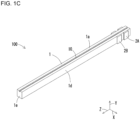
- FIG. 1C is an external perspective view of the piezoelectric element
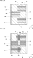
- FIG. 2A is a cross-sectional view taken along line A-A in FIG. 1A
- FIG. 2B is a cross-sectional view taken along line B-B in FIG. 1A
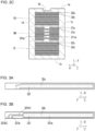
- FIG. 2C is a cross-sectional view taken along line C-C in FIG. 1A
- a piezoelectric element 100 includes a stack 1 including internal electrodes 3 and piezoelectric layers 4 that are stacked on one another and surface electrodes 2 located on side surfaces of the stack 1 and electrically connected to the internal electrodes 3.
- the piezoelectric element 100 is a piezoelectric actuator that applies a voltage to the internal electrodes 3 through the surface electrodes 2 to cause the stacked piezoelectric layers 4 to deform by bending.
- the piezoelectric element 100 according to the present embodiment is, for example, a rectangular or quadrangular prism, and has one end in its longitudinal or axial direction movable as the piezoelectric element 100 deforms by bending.
- the surface electrodes 2 are located on the two side surfaces of the other end opposite to the movable end.
- the surface electrodes 2 include surface electrodes 2A on the two side surfaces of the other end and surface electrodes 2B on the two side surfaces nearer the middle than the surface electrodes 2A.
- the longitudinal or the axial direction is hereafter referred to as Z-direction.
- the direction orthogonal to Z-direction and connecting the two side surfaces on which the surface electrodes 2 are located is referred to as X-direction.
- the stacking direction orthogonal to Z- and X-directions and in which the internal electrodes 3 and the piezoelectric layers 4 are stacked is referred to as Y-direction.
- the stack 1 includes the piezoelectric layers 4 being stacked and the internal electrodes 3 each between adjacent piezoelectric layers 4.
- the stack 1 includes an upper surface 1a and a lower surface 1b orthogonal to the stacking direction (Y-direction), two side surfaces 1c and 1d orthogonal to a width direction (X-direction), and a front surface 1e and a rear surface 1f orthogonal to the longitudinal direction (Z-direction).
- the surface electrodes 2 are located on the two side surfaces 1c and 1d.
- the internal electrodes 3 are exposed on the side surfaces of the other end of the stack 1 and are electrically connected to the surface electrodes 2.
- the piezoelectric layers 4 are made of a ceramic material having piezoelectric properties.
- the ceramic material include perovskite-type oxides containing lead zirconate titanate (PbZrO 3 -PbTiO 3 ), lithium niobate (LiNbO 3 ), and lithium tantalate (LiTaO 3 ).
- the internal electrodes 3 may include, for example, a conductor containing, as a main component, silver or a silver-palladium alloy less reactive with a ceramic material or a conductor containing copper or platinum.
- the surface electrodes 2 may be made of, for example, the same or similar materials to the internal electrode 3, and may further be plated to prevent oxidation.
- the internal electrodes 3 include first electrodes 31 that apply a voltage to the piezoelectric layers 4 to cause the stack 1 to bend in a first direction (X-direction) orthogonal to the longitudinal direction (Z-direction) of the stack 1 and second electrodes 32 that apply a voltage to the piezoelectric layers 4 to cause the stack 1 to bend in a second direction (Y-direction) orthogonal to the longitudinal direction and to the first direction.
- the stack 1 is divided into substantially three areas in the stacking direction (Y-direction). The three areas include a middle area 1M for causing the piezoelectric element 100 to deform by bending in X-direction (lateral direction).
- the first electrodes 31 are located in the middle area 1M.
- the three areas further include an upper area 1U and a lower area 1L for causing the piezoelectric element 100 to deform by bending in Y-direction (vertical direction).
- the second electrodes 32 are located in the upper area 1U and the lower area 1L.
- the first electrodes 31 in the middle area 1M receive a voltage to have an expanded right portion and a contracted left portion. This causes the piezoelectric element 100 to bend leftward.
- the first electrodes 31 receive a voltage to have a contracted right portion and an expanded left portion. This causes the piezoelectric element 100 to bend rightward.
- the second electrodes 32 receive a voltage to have an expanded upper area 1U and a contracted lower area 1L. This causes the piezoelectric element 100 to bend downward.
- the second electrodes 32 receive a voltage to have a contracted upper area 1U and an expanded lower area 1L. This causes the piezoelectric element 100 to bend upward.
- FIGs. 3A to 3F illustrate example patterns on the internal electrodes 3 in the present embodiment. These are example patterns on the second electrodes 32 in the upper area 1U, the first electrodes 31 in the middle area 1M, and the second electrodes 32 in the lower area 1L.
- the patterns illustrated in FIGs. 3A and 3B are defined on the second electrodes 32 in the upper area 1U.
- the patterns illustrated in FIGs. 3C and 3D are defined on the first electrodes 31 in the middle area 1M.
- the patterns illustrated in FIGs. 3E and 3F are defined on the second electrodes 32 in the lower area 1L.
- Each area includes the internal electrodes 3 having two different patterns.
- the internal electrodes 3 having two different patterns are alternately located between the piezoelectric layers 4 in Y-direction.
- a voltage is applied externally through the surface electrodes 2 to generate a potential difference between the two different internal electrodes 3.
- the piezoelectric element 100 can deform by bending in X- and Y-directions as described above.
- a voltage applied to the surface electrodes 2 can be varied to control the degree of deformation and the direction of bending.
- the second electrodes 32 in the upper area 1U correspond to second electrodes 32a each illustrated in FIG. 3A and to second electrodes 32b each illustrated in FIG. 3B .
- the second electrodes 32 in the lower area 1L correspond to second electrodes 32c each illustrated in FIG. 3E and to second electrodes 32d each illustrated in FIG. 3F .
- Each second electrode 32b illustrated in FIG. 3B includes a first conductor 321 including a rectangular portion 321a extending in the longitudinal direction and an extension 321b having one end continuous with the rectangular portion 321a and the other end exposed on the side surface of the stack 1 and connected to the surface electrode 2A.
- the second electrode 32d illustrated in FIG. 3F has the same pattern as the second electrode 32b illustrated in FIG. 3B .
- the second electrode 32d includes the first conductor 321, in the same or similar manner as the second electrode 32b.
- the extension 321b is, for example, substantially L-shaped.
- the extension 321b has one end continuous with the middle of the rectangular portion 321a and extending linearly in Z-direction, and the other end bending at right angles toward the side surface of the stack 1 to be exposed on the side surface of the stack 1.
- the substantially L-shaped extension 321b includes a wire 321b1 having a smaller width than the rectangular portion 321a and a connection 321b2 continuous with the wire 321b 1.
- the connection 321b2 is exposed on the side surface and connected to the surface electrodes 2.
- the second electrode 32a in FIG. 3A and the second electrode 32c in FIG. 3E include the rectangular portions 321a and have patterns symmetrical to each other with respect to Z-direction.
- the piezoelectric element 100 may have any dimensions.
- the piezoelectric element 100 may have a length of 1 to 3 mm in X-direction, a length of 1 to 2 mm in Y-direction, and a length of 20 to 50 mm in Z-direction.
- the internal electrodes 3 may each have a thickness of 0.1 to 5 ⁇ m.
- the piezoelectric layers 4 may each have a thickness of 0.01 to 0. 1 mm.
- the first electrodes 31 in the middle area 1M correspond to first electrodes 31a each illustrated in FIG. 3C and to first electrodes 31b each illustrated in FIG. 3D .
- Each first electrode 31a includes a pair of strips 311a extending parallel to each other in the longitudinal direction. In the present embodiment, for example, the strips 311a are spaced from each other across a middle portion of the stack 1 in the width direction.
- Each first electrode 3 1b has a pattern symmetrical to the pattern on the second electrode 32b with respect to Z-direction. More specifically, in the present embodiment, the first electrode 31b in FIG. 3D includes a first conductor 321' that is symmetrical to the first conductor 321 in the second electrode 32b in FIG. 3B with respect to Z-direction.
- the second electrode 32d in FIG. 3F includes the same first conductor 321 as the second electrode 32b in FIG. 3B .
- the second electrode 32a illustrated in FIG. 3A and the second electrode 32c illustrated in FIG. 3E include a first conductor 321 and a first conductor 321' having shapes similar to the shapes of the first conductor 321 and the first conductor 321'.
- the stack 1 includes a groove 10 extending in the longitudinal direction (Z-direction) on at least one of the upper surface 1a or the lower surface 1b.
- the piezoelectric layers 4 include inactive areas with an insufficient level of voltage being applied.
- the inactive areas include, in the upper area 1U and the lower area 1L, the outermost layers including the upper and lower surfaces 1a and 1b of the stack 1 that are not located between electrodes, and, in the middle area 1M, the middle portion in the width direction located between the pair of strips 311a.
- the inactive areas in the upper area 1U, the middle area 1M, and the lower area 1L obstruct the deformation and cause insufficient deformation of the piezoelectric element 100.
- the groove 10 on at least one of the upper surface 1a or the lower surface 1b of the stack 1 reduces the inactive area in the upper area 1U or the lower area 1L, thus increasing the degree of deformation.
- the stack 1 includes the groove 10 on the upper surface 1a to reduce the inactive area in the upper area 1U.
- the groove 10 has a rectangular cross section.
- the groove 10 may have a U- or V-shaped cross section, or may be a part of a circle (including an ellipse) such as a semicircle.
- the groove 10 may extend continuously or partially discontinuously (intermittently) in the longitudinal direction on the upper surface 1a of the stack 1.
- the intermittent groove 10 may have, for example, the total length greater than or equal to 50% of the length (longitudinal dimension) of the stack 1.
- the groove 10 may have a depth of, for example, 0.01 to 5% inclusive of the thickness of the stack 1 (dimension in the stacking direction).
- the groove 10 may have a width of, for example, 0.1 to 20% inclusive of the width of the stack 1 (dimension in the width dimension).
- the groove 10 may be at any position on the upper surface 1a of the stack 1 to reduce the inactive area.
- the groove 10 is located in a middle portion of the upper surface 1a in the width direction.
- the groove 10 in the middle portion in the width direction allows the piezoelectric element 100 to increase the degree of deformation equally in one direction along the width and in the other direction along the width.
- the middle area 1M includes the inactive area in the middle portion in the width direction between the pair of strips 311a. The groove 10 in the middle portion in the width direction reduces the inactive area in the middle area 1M that obstructs the deformation.
- One surface electrode 2A is electrically connected to the second electrodes 32b in the upper area 1U and the second electrodes 32d in the lower area 1L.
- the other surface electrode 2A is electrically connected to the first electrodes 31b in the middle area 1M.
- One surface electrode 2B is electrically connected to the second electrodes 32a in the upper area 1U and the first electrodes 31a (at one side) in the middle area 1M.
- the other surface electrode 2B is electrically connected to the first electrodes 31a (at the other side) in the middle area 1M and the second electrodes 32c in the lower area 1L.
- the polarization direction of the piezoelectric layers 4 includes a first direction and a second direction.
- One side of each of the upper area 1U and the middle area 1M corresponds to the first direction.
- the other side of each of the lower area 1L and the middle area 1M corresponds to the second direction opposite to the first direction.
- the surface electrodes 2A are set to a ground potential.
- a voltage of -64 V is applied to one surface electrode 2B and +64 V to the other surface electrode 2B to polarize the piezoelectric layers 4 as described above.
- a constant voltage is applied to each of the surface electrodes 2B during operation.
- An example voltage to be applied is +11 V to one surface electrode 2B and +61 V to the other surface electrode 2B.
- a voltage of 0 to +72 V applied to both the surface electrodes 2A can cause the piezoelectric element 100 to deform by bending in an intended direction.
- a voltage of +72 V is applied to one surface electrode 2A and +36 V to the other surface electrode 2A to cause the piezoelectric element 100 to deform by bending (at a maximum degree) in one Y-direction (upward)
- a voltage of 0 V is applied to one surface electrode 2A and +36 V to the other surface electrode 2A to cause the piezoelectric element 100 to deform by bending (at a maximum degree) in the other Y-direction (downward).
- a voltage of 0 to +72 V is applied to one surface electrode 2A
- a constant voltage of +36 V is applied to the other surface electrode 2A to adjust the degree by which the deformation by bending occurs in Y-direction.
- a voltage of +36 V is applied to one surface electrode 2A and +72 V to the other surface electrode 2A to cause the piezoelectric element 100 to deform by bending (at a maximum degree) in one X-direction (rightward).
- a voltage of +36 V is applied to one surface electrode 2A and 0 V to the other surface electrode 2A to cause the piezoelectric element 100 to deform by bending (at a maximum degree) in the other X-direction (leftward).
- a constant voltage of +36 V is applied to one surface electrode 2A, and a voltage of 0 to +72 V is applied to the other surface electrode 2A to adjust the degree by which the deformation by bending occurs in X-direction.
- a voltage to be applied to both the surface electrodes 2A is varied within the range of 0 to +72 V to cause the deformation by bending in an oblique direction.
- FIG. 4 is a cross-sectional view of a piezoelectric element according to another embodiment.
- the cross-sectional view in FIG. 4 corresponds to the cross-sectional view illustrated in FIG. 2C .
- the stack 1 includes round corners at which the upper surface 1a including the groove 10 intersects with the side surfaces 1c and 1d.
- the piezoelectric element 100 according to the present embodiment includes chamfered and round corners at which the upper surface 1a and the side surfaces 1c and 1d of the stack 1 intersect with each other.
- the chamfered corners of the upper surface 1a of the stack 1 can further reduce the inactive area in the upper area 1U, thus increasing the degree of deformation.
- the chamfered corners can also reduce chips and cracks in the corners of the upper area 1U.
- FIG. 5 is a cross-sectional view of a piezoelectric element according to another embodiment.
- the cross-sectional view in FIG. 5 corresponds to the cross-sectional view illustrated in FIG. 2C .
- the stack 1 includes the groove 10 on the lower surface 1b in addition to the upper surface 1a.
- the groove 10 may be at any position on the lower surface 1b of the stack 1 to reduce the inactive area.
- the groove 10 is located in a middle portion of the lower surface 1b in the width direction.
- the groove 10 in the middle portion in the width direction allows the piezoelectric element 100 to increase the degree of deformation equally in one direction along the width and in the other direction along the width.
- the groove 10 on the upper surface 1a and the groove 10 on the lower surface 1b may have, for example, the same shape and dimensions, the same shape and different dimensions, or different shapes.
- the groove 10 on the upper surface 1a and the groove 10 on the lower surface 1b may be, for example, at the same position or at different positions as viewed in plan.
- the groove 10 on the lower surface 1b can reduce the inactive area in the lower area 1L, thus increasing the degree of deformation.
- the stack 1 may include round corners at which the lower surface 1b including the groove 10 intersect with the side surfaces 1c and 1d.
- the chamfered corners of the lower surface 1b of the stack 1 can further reduce the inactive area in the lower area 1L, thus increasing the degree of deformation.
- the chamfered corners can also reduce chips and cracks in the corners of the lower area 1L.
- FIG. 6 is a cross-sectional view of a piezoelectric element according to another embodiment.
- the cross-sectional view in FIG. 6 corresponds to the cross-sectional view illustrated in FIG. 2C .
- the rectangular portions 321a of the second electrodes 32a and the second electrodes 32b in the upper area 1U of the stack 1 each include at least one of end portions in the width direction arched upward in the stacking direction.
- Each rectangular portion 321a includes three portions in the width direction. The three portions each extend in the longitudinal direction.
- Each rectangular portion 321a includes, for example, an end portion 321a1 adjacent to the side surface 1c, an end portion 321a2 adjacent to the side surface 1d, and a middle portion 321a3 between the end portions 321a1 and 321a2.
- the three portions may not be defined by clear boundaries. At least one of the end portion 321a1 adjacent to the side surface 1c or the end portion 321a2 adjacent to the side surface 1d is arched upward in the stacking direction. In the present embodiment, both the end portion 321a1 adjacent to the side surface 1c and the end portion 321a2 adjacent to the side surface 1d are arched upward in the stacking direction.
- the rectangular portion 321a of the second electrode 32 being a flat plate
- the piezoelectric element 100 deforming in the width direction deforms in the planar direction of the flat plate.
- the plate is less likely to deform in the planar direction than in other directions and may thus obstruct the deformation of the piezoelectric element 100 in the width direction.
- the rectangular portions 321a are at least partially arched upward in the stacking direction. This causes the stack 1 to deform easily in the width direction, thus increasing the degree of deformation of the piezoelectric element 100 in the width direction.
- the end portions 321a1 and the end portion 321a2 are, for example, arched upward and outward in the stacking direction.
- the middle portion 321a3 may also be arched upward in the stacking direction, in the same or similar manner as the two end portions 321a1 and 321a2.
- the rectangular portions 321a of the second electrodes 32c and the second electrodes 32d in the lower area 1L may each include at least one of the end portions in the width direction arched upward in the stacking direction, in the same or similar manner as in the upper area 1U.
- the two end portions of each rectangular portion 321a in the width direction are arched upward and outward in the stacking direction.
- the rectangular portions 321a are at least partially arched upward in the stacking direction. This causes the stack 1 to easily deform in the width direction, thus further increasing the degree of deformation of the piezoelectric element 100 in the width direction.
- FIG. 7 is a cross-sectional view of a piezoelectric element according to another embodiment.
- the cross-sectional view in FIG. 7 corresponds to the cross-sectional view illustrated in FIG. 2C .
- the rectangular portions 321a of the second electrodes 32a and the second electrodes 32b in the upper area 1U of the stack 1 each include at least one of the end portions in the width direction arched upward in the stacking direction.
- the arched end portions have their outer portions in the width direction located more outward in the stacking direction than their inner portions in the width direction. More specifically, the arched end portions of the rectangular portions 321a are inclined with respect to the upper surface 1a and the lower surface 1b of the stack 1.
- the rectangular portions 321a include, for example, the end portions 321a1 adjacent to the side surface 1c and the end portions 321a2 adjacent to the side surface 1d arched upward in the stacking direction and inclined with respect to the upper surface 1a and the lower surface 1b of the stack 1.
- the upper area 1U of the stack 1 at least a part of each rectangular portion 321a is inclined to cause the stack 1 to easily deform in the width direction, thus increasing the degree of deformation of the piezoelectric element 100 in the width direction.
- the rectangular portions 321a of the second electrodes 32c and the second electrodes 32d in the lower area 1L may each include at least one of the end positions in the width direction arched upward in the stacking direction with the arched end portions including their outer portions in the width direction located more outward in the stacking direction than their inner portions in the width direction, in the same or similar manner as in the upper area 1U.
- the two end portions of the rectangular portion 321a in the width direction are arched upward and outward in the stacking direction and inclined with respect to the upper surface 1a and the lower surface 1b of the stack 1.
- at least a part of each rectangular portion 321a is inclined to cause the stack 1 to easily deform in the width direction, thus increasing the degree of deformation of the piezoelectric element 100 in the width direction.
- FIG. 8 is a cross-sectional view of a piezoelectric element according to another embodiment.
- the cross-sectional view in FIG. 8 corresponds to the cross-sectional view illustrated in FIG. 2C or FIG. 4 .
- the stack 1 includes a groove 10A located on at least one of the upper surface 1a or the lower surface 1b.
- the groove 10A extends in the longitudinal direction (Z-direction) and may have, for example, a curved bottom in the shape of, for example, a recess or a concave.
- the groove 10A may have, for example, curved edges smoothly connected to the upper surface 1a as viewed in the cross section as illustrated in FIG. 8 . This reduces concentration of stress at the bottom of the groove 10A and thus reduces chips and cracks in the edges of the groove 10A.
- a piezoelectric element includes a stack including a plurality of internal electrodes and a plurality of piezoelectric layers alternately stacked on one another, and a surface electrode located on a side surface of the stack and electrically connected to the plurality of internal electrodes.
- the stack is a rectangular prism with a longitudinal direction orthogonal to a stacking direction.
- the plurality of internal electrodes includes a first electrode that applies a voltage to the plurality of piezoelectric layers to cause the stack to bend in the stacking direction, and a second electrode that applies a voltage to the plurality of piezoelectric layers to cause the stack to bend in a width direction orthogonal to the stacking direction and to the longitudinal direction.
- the stack includes a groove extending in the longitudinal direction on at least one of an upper surface or a lower surface of the stack orthogonal to the stacking direction.
- the piezoelectric element according to one or more embodiments of the present disclosure reduces the inactive area to increase the degree of deformation.
Landscapes
- General Electrical Machinery Utilizing Piezoelectricity, Electrostriction Or Magnetostriction (AREA)
Abstract
Description
- The present disclosure relates to a piezoelectric element.
- A known technique is described in, for example,
Patent Literature 1. - Patent Literature 1:
Japanese Patent No. 4240472 - In an aspect of the present disclosure, a piezoelectric element includes a stack including a plurality of internal electrodes and a plurality of piezoelectric layers alternately stacked on one another, and a surface electrode located on a side surface of the stack and electrically connected to the plurality of internal electrodes. The stack is a rectangular prism with a longitudinal direction orthogonal to a stacking direction. The plurality of internal electrodes includes a first electrode that applies a voltage to the plurality of piezoelectric layers to cause the stack to bend in the stacking direction, and a second electrode that applies a voltage to the plurality of piezoelectric layers to cause the stack to bend in a width direction orthogonal to the stacking direction and to the longitudinal direction. The stack includes a groove extending in the longitudinal direction on at least one of an upper surface or a lower surface of the stack orthogonal to the stacking direction.
- The objects, features, and advantages of the present disclosure will become more apparent from the following detailed description and the drawings.
-
FIG. 1A is an external plan view of a piezoelectric element. -
FIG. 1B is an external side view of the piezoelectric element. -
FIG. 1C is an external perspective view of the piezoelectric element. -
FIG. 2A is a cross-sectional view taken along line A-A inFIG. 1A . -
FIG. 2B is a cross-sectional view taken along line B-B inFIG. 1A . -
FIG. 2C is a cross-sectional view taken along line C-C inFIG. 1A . -
FIG. 3A is a diagram of an internal electrode pattern. -
FIG. 3B is a diagram of an internal electrode pattern. -
FIG. 3C is a diagram of an internal electrode pattern. -
FIG. 3D is a diagram of an internal electrode pattern. -
FIG. 3E is a diagram of an internal electrode pattern. -
FIG. 3F is a diagram of an internal electrode pattern. -
FIG. 4 is a cross-sectional view of a piezoelectric element according to another embodiment. -
FIG. 5 is a cross-sectional view of a piezoelectric element according to another embodiment. -
FIG. 6 is a cross-sectional view of a piezoelectric element according to another embodiment. -
FIG. 7 is a cross-sectional view of a piezoelectric element according to another embodiment. -
FIG. 8 is a cross-sectional view of a piezoelectric element according to another embodiment. - A piezoelectric element with the structure that forms the basis of a piezoelectric element according to one or more embodiments of the present disclosure includes piezoelectric layers and internal electrodes that are stacked on one another. The piezoelectric element is used as a piezoelectric actuator that deforms by bending in response to a voltage applied to the internal electrodes. Such a piezoelectric actuator can deform slightly with high precision.
- A piezoelectric actuator described in
Patent Literature 1 is elongated along Z-axis and has an end movable in the XY plane. -
FIG. 1A is an external plan view of a piezoelectric element, andFIG. 1B is an external side view of the piezoelectric element.FIG. 1C is an external perspective view of the piezoelectric element.FIG. 2A is a cross-sectional view taken along line A-A inFIG. 1A .FIG. 2B is a cross-sectional view taken along line B-B inFIG. 1A .FIG. 2C is a cross-sectional view taken along line C-C inFIG. 1A . Apiezoelectric element 100 includes astack 1 including internal electrodes 3 and piezoelectric layers 4 that are stacked on one another andsurface electrodes 2 located on side surfaces of thestack 1 and electrically connected to the internal electrodes 3. In the present embodiment, thepiezoelectric element 100 is a piezoelectric actuator that applies a voltage to the internal electrodes 3 through thesurface electrodes 2 to cause the stacked piezoelectric layers 4 to deform by bending. As illustrated inFIGs. 1A to 1C , thepiezoelectric element 100 according to the present embodiment is, for example, a rectangular or quadrangular prism, and has one end in its longitudinal or axial direction movable as thepiezoelectric element 100 deforms by bending. Thesurface electrodes 2 are located on the two side surfaces of the other end opposite to the movable end. Thesurface electrodes 2 includesurface electrodes 2A on the two side surfaces of the other end andsurface electrodes 2B on the two side surfaces nearer the middle than thesurface electrodes 2A. The longitudinal or the axial direction is hereafter referred to as Z-direction. The direction orthogonal to Z-direction and connecting the two side surfaces on which thesurface electrodes 2 are located is referred to as X-direction. The stacking direction orthogonal to Z- and X-directions and in which the internal electrodes 3 and the piezoelectric layers 4 are stacked is referred to as Y-direction. - As illustrated in the cross-sectional view of
FIG. 2A or other figures, thestack 1 includes the piezoelectric layers 4 being stacked and the internal electrodes 3 each between adjacent piezoelectric layers 4. Thestack 1 includes anupper surface 1a and alower surface 1b orthogonal to the stacking direction (Y-direction), twoside surfaces front surface 1e and arear surface 1f orthogonal to the longitudinal direction (Z-direction). Thesurface electrodes 2 are located on the twoside surfaces stack 1 and are electrically connected to thesurface electrodes 2. The piezoelectric layers 4 are made of a ceramic material having piezoelectric properties. Examples of the ceramic material include perovskite-type oxides containing lead zirconate titanate (PbZrO3-PbTiO3), lithium niobate (LiNbO3), and lithium tantalate (LiTaO3). The internal electrodes 3 may include, for example, a conductor containing, as a main component, silver or a silver-palladium alloy less reactive with a ceramic material or a conductor containing copper or platinum. Thesurface electrodes 2 may be made of, for example, the same or similar materials to the internal electrode 3, and may further be plated to prevent oxidation. - As described in detail later, the internal electrodes 3 include first electrodes 31 that apply a voltage to the piezoelectric layers 4 to cause the
stack 1 to bend in a first direction (X-direction) orthogonal to the longitudinal direction (Z-direction) of thestack 1 and second electrodes 32 that apply a voltage to the piezoelectric layers 4 to cause thestack 1 to bend in a second direction (Y-direction) orthogonal to the longitudinal direction and to the first direction. For example, thestack 1 is divided into substantially three areas in the stacking direction (Y-direction). The three areas include amiddle area 1M for causing thepiezoelectric element 100 to deform by bending in X-direction (lateral direction). The first electrodes 31 are located in themiddle area 1M. The three areas further include anupper area 1U and alower area 1L for causing thepiezoelectric element 100 to deform by bending in Y-direction (vertical direction). The second electrodes 32 are located in theupper area 1U and thelower area 1L. - For example, to cause the
piezoelectric element 100 to deform by bending in X-direction, the first electrodes 31 in themiddle area 1M receive a voltage to have an expanded right portion and a contracted left portion. This causes thepiezoelectric element 100 to bend leftward. The first electrodes 31 receive a voltage to have a contracted right portion and an expanded left portion. This causes thepiezoelectric element 100 to bend rightward. Similarly, for example, to cause thepiezoelectric element 100 to deform by bending in Y-direction, the second electrodes 32 receive a voltage to have an expandedupper area 1U and a contractedlower area 1L. This causes thepiezoelectric element 100 to bend downward. The second electrodes 32 receive a voltage to have a contractedupper area 1U and an expandedlower area 1L. This causes thepiezoelectric element 100 to bend upward. -
FIGs. 3A to 3F illustrate example patterns on the internal electrodes 3 in the present embodiment. These are example patterns on the second electrodes 32 in theupper area 1U, the first electrodes 31 in themiddle area 1M, and the second electrodes 32 in thelower area 1L. The patterns illustrated inFIGs. 3A and 3B are defined on the second electrodes 32 in theupper area 1U. The patterns illustrated inFIGs. 3C and 3D are defined on the first electrodes 31 in themiddle area 1M. The patterns illustrated inFIGs. 3E and 3F are defined on the second electrodes 32 in thelower area 1L. Each area includes the internal electrodes 3 having two different patterns. The internal electrodes 3 having two different patterns are alternately located between the piezoelectric layers 4 in Y-direction. During the operation of thepiezoelectric element 100, a voltage is applied externally through thesurface electrodes 2 to generate a potential difference between the two different internal electrodes 3. Thepiezoelectric element 100 can deform by bending in X- and Y-directions as described above. A voltage applied to thesurface electrodes 2 can be varied to control the degree of deformation and the direction of bending. - The second electrodes 32 in the
upper area 1U correspond tosecond electrodes 32a each illustrated inFIG. 3A and tosecond electrodes 32b each illustrated inFIG. 3B . The second electrodes 32 in thelower area 1L correspond tosecond electrodes 32c each illustrated inFIG. 3E and tosecond electrodes 32d each illustrated inFIG. 3F . Eachsecond electrode 32b illustrated inFIG. 3B includes afirst conductor 321 including arectangular portion 321a extending in the longitudinal direction and anextension 321b having one end continuous with therectangular portion 321a and the other end exposed on the side surface of thestack 1 and connected to thesurface electrode 2A. Thesecond electrode 32d illustrated inFIG. 3F has the same pattern as thesecond electrode 32b illustrated inFIG. 3B . Thesecond electrode 32d includes thefirst conductor 321, in the same or similar manner as thesecond electrode 32b. Theextension 321b is, for example, substantially L-shaped. Theextension 321b has one end continuous with the middle of therectangular portion 321a and extending linearly in Z-direction, and the other end bending at right angles toward the side surface of thestack 1 to be exposed on the side surface of thestack 1. The substantially L-shapedextension 321b includes a wire 321b1 having a smaller width than therectangular portion 321a and a connection 321b2 continuous with thewire 321bsurface electrodes 2. Thesecond electrode 32a inFIG. 3A and thesecond electrode 32c inFIG. 3E include therectangular portions 321a and have patterns symmetrical to each other with respect to Z-direction. - The
piezoelectric element 100 may have any dimensions. For example, thepiezoelectric element 100 may have a length of 1 to 3 mm in X-direction, a length of 1 to 2 mm in Y-direction, and a length of 20 to 50 mm in Z-direction. The internal electrodes 3 may each have a thickness of 0.1 to 5 µm. The piezoelectric layers 4 may each have a thickness of 0.01 to 0. 1 mm. - The first electrodes 31 in the
middle area 1M correspond tofirst electrodes 31a each illustrated inFIG. 3C and tofirst electrodes 31b each illustrated inFIG. 3D . Eachfirst electrode 31a includes a pair ofstrips 311a extending parallel to each other in the longitudinal direction. In the present embodiment, for example, thestrips 311a are spaced from each other across a middle portion of thestack 1 in the width direction. Each first electrode 3 1b has a pattern symmetrical to the pattern on thesecond electrode 32b with respect to Z-direction. More specifically, in the present embodiment, thefirst electrode 31b inFIG. 3D includes a first conductor 321' that is symmetrical to thefirst conductor 321 in thesecond electrode 32b inFIG. 3B with respect to Z-direction. In the present embodiment, thesecond electrode 32d inFIG. 3F includes the samefirst conductor 321 as thesecond electrode 32b inFIG. 3B . Additionally, thesecond electrode 32a illustrated inFIG. 3A and thesecond electrode 32c illustrated inFIG. 3E include afirst conductor 321 and a first conductor 321' having shapes similar to the shapes of thefirst conductor 321 and the first conductor 321'. - The
stack 1 includes agroove 10 extending in the longitudinal direction (Z-direction) on at least one of theupper surface 1a or thelower surface 1b. When thepiezoelectric element 100 deforms, the piezoelectric layers 4 include inactive areas with an insufficient level of voltage being applied. For example, the inactive areas include, in theupper area 1U and thelower area 1L, the outermost layers including the upper andlower surfaces stack 1 that are not located between electrodes, and, in themiddle area 1M, the middle portion in the width direction located between the pair ofstrips 311a. When thepiezoelectric element 100 deforms in the width direction, the inactive areas in theupper area 1U, themiddle area 1M, and thelower area 1L obstruct the deformation and cause insufficient deformation of thepiezoelectric element 100. Thegroove 10 on at least one of theupper surface 1a or thelower surface 1b of thestack 1 reduces the inactive area in theupper area 1U or thelower area 1L, thus increasing the degree of deformation. In the present embodiment, thestack 1 includes thegroove 10 on theupper surface 1a to reduce the inactive area in theupper area 1U. - In the present embodiment, the
groove 10 has a rectangular cross section. Thegroove 10 may have a U- or V-shaped cross section, or may be a part of a circle (including an ellipse) such as a semicircle. Thegroove 10 may extend continuously or partially discontinuously (intermittently) in the longitudinal direction on theupper surface 1a of thestack 1. Theintermittent groove 10 may have, for example, the total length greater than or equal to 50% of the length (longitudinal dimension) of thestack 1. Thegroove 10 may have a depth of, for example, 0.01 to 5% inclusive of the thickness of the stack 1 (dimension in the stacking direction). Thegroove 10 may have a width of, for example, 0.1 to 20% inclusive of the width of the stack 1 (dimension in the width dimension). - The
groove 10 may be at any position on theupper surface 1a of thestack 1 to reduce the inactive area. In the present embodiment, for example, thegroove 10 is located in a middle portion of theupper surface 1a in the width direction. Thegroove 10 in the middle portion in the width direction allows thepiezoelectric element 100 to increase the degree of deformation equally in one direction along the width and in the other direction along the width. Themiddle area 1M includes the inactive area in the middle portion in the width direction between the pair ofstrips 311a. Thegroove 10 in the middle portion in the width direction reduces the inactive area in themiddle area 1M that obstructs the deformation. - The operation of the
piezoelectric element 100 will be described briefly. First, the electrical connection between thesurface electrodes 2 and the internal electrodes 3 will be described. One surface electrode 2Ais electrically connected to thesecond electrodes 32b in theupper area 1U and thesecond electrodes 32d in thelower area 1L. The other surface electrode 2Ais electrically connected to thefirst electrodes 31b in themiddle area 1M. Onesurface electrode 2B is electrically connected to thesecond electrodes 32a in theupper area 1U and thefirst electrodes 31a (at one side) in themiddle area 1M. Theother surface electrode 2B is electrically connected to thefirst electrodes 31a (at the other side) in themiddle area 1M and thesecond electrodes 32c in thelower area 1L. The polarization direction of the piezoelectric layers 4 includes a first direction and a second direction. One side of each of theupper area 1U and themiddle area 1M corresponds to the first direction. The other side of each of thelower area 1L and themiddle area 1M corresponds to the second direction opposite to the first direction. For example, thesurface electrodes 2A are set to a ground potential. A voltage of -64 V is applied to onesurface electrode 2B and +64 V to theother surface electrode 2B to polarize the piezoelectric layers 4 as described above. - A constant voltage is applied to each of the
surface electrodes 2B during operation. An example voltage to be applied is +11 V to onesurface electrode 2B and +61 V to theother surface electrode 2B. A voltage of 0 to +72 V applied to both thesurface electrodes 2A can cause thepiezoelectric element 100 to deform by bending in an intended direction. For example, a voltage of +72 V is applied to onesurface electrode 2A and +36 V to theother surface electrode 2A to cause thepiezoelectric element 100 to deform by bending (at a maximum degree) in one Y-direction (upward), and a voltage of 0 V is applied to onesurface electrode 2A and +36 V to theother surface electrode 2A to cause thepiezoelectric element 100 to deform by bending (at a maximum degree) in the other Y-direction (downward). In other words, a voltage of 0 to +72 V is applied to onesurface electrode 2A, and a constant voltage of +36 V is applied to theother surface electrode 2A to adjust the degree by which the deformation by bending occurs in Y-direction. For example, a voltage of +36 V is applied to onesurface electrode 2A and +72 V to theother surface electrode 2A to cause thepiezoelectric element 100 to deform by bending (at a maximum degree) in one X-direction (rightward). A voltage of +36 V is applied to onesurface electrode 2A and 0 V to theother surface electrode 2A to cause thepiezoelectric element 100 to deform by bending (at a maximum degree) in the other X-direction (leftward). In other words, a constant voltage of +36 V is applied to onesurface electrode 2A, and a voltage of 0 to +72 V is applied to theother surface electrode 2A to adjust the degree by which the deformation by bending occurs in X-direction. A voltage to be applied to both thesurface electrodes 2A is varied within the range of 0 to +72 V to cause the deformation by bending in an oblique direction. -
FIG. 4 is a cross-sectional view of a piezoelectric element according to another embodiment. The cross-sectional view inFIG. 4 corresponds to the cross-sectional view illustrated inFIG. 2C . In the present embodiment, thestack 1 includes round corners at which theupper surface 1a including thegroove 10 intersects with the side surfaces 1c and 1d. More specifically, thepiezoelectric element 100 according to the present embodiment includes chamfered and round corners at which theupper surface 1a and the side surfaces 1c and 1d of thestack 1 intersect with each other. The chamfered corners of theupper surface 1a of thestack 1 can further reduce the inactive area in theupper area 1U, thus increasing the degree of deformation. The chamfered corners can also reduce chips and cracks in the corners of theupper area 1U. -
FIG. 5 is a cross-sectional view of a piezoelectric element according to another embodiment. The cross-sectional view inFIG. 5 corresponds to the cross-sectional view illustrated inFIG. 2C . In the present embodiment, thestack 1 includes thegroove 10 on thelower surface 1b in addition to theupper surface 1a. Thegroove 10 may be at any position on thelower surface 1b of thestack 1 to reduce the inactive area. In the present embodiment, for example, thegroove 10 is located in a middle portion of thelower surface 1b in the width direction. Thegroove 10 in the middle portion in the width direction allows thepiezoelectric element 100 to increase the degree of deformation equally in one direction along the width and in the other direction along the width. Thegroove 10 on theupper surface 1a and thegroove 10 on thelower surface 1b may have, for example, the same shape and dimensions, the same shape and different dimensions, or different shapes. Thegroove 10 on theupper surface 1a and thegroove 10 on thelower surface 1b may be, for example, at the same position or at different positions as viewed in plan. Thegroove 10 on thelower surface 1b can reduce the inactive area in thelower area 1L, thus increasing the degree of deformation. Thestack 1 may include round corners at which thelower surface 1b including thegroove 10 intersect with the side surfaces 1c and 1d. The chamfered corners of thelower surface 1b of thestack 1 can further reduce the inactive area in thelower area 1L, thus increasing the degree of deformation. The chamfered corners can also reduce chips and cracks in the corners of thelower area 1L. -
FIG. 6 is a cross-sectional view of a piezoelectric element according to another embodiment. The cross-sectional view inFIG. 6 corresponds to the cross-sectional view illustrated inFIG. 2C . Therectangular portions 321a of thesecond electrodes 32a and thesecond electrodes 32b in theupper area 1U of thestack 1 each include at least one of end portions in the width direction arched upward in the stacking direction. Eachrectangular portion 321a includes three portions in the width direction. The three portions each extend in the longitudinal direction. Eachrectangular portion 321a includes, for example, an end portion 321a1 adjacent to theside surface 1c, an end portion 321a2 adjacent to theside surface 1d, and a middle portion 321a3 between the end portions 321a1 and 321a2. The three portions may not be defined by clear boundaries. At least one of the end portion 321a1 adjacent to theside surface 1c or the end portion 321a2 adjacent to theside surface 1d is arched upward in the stacking direction. In the present embodiment, both the end portion 321a1 adjacent to theside surface 1c and the end portion 321a2 adjacent to theside surface 1d are arched upward in the stacking direction. With therectangular portion 321a of the second electrode 32 being a flat plate, thepiezoelectric element 100 deforming in the width direction deforms in the planar direction of the flat plate. The plate is less likely to deform in the planar direction than in other directions and may thus obstruct the deformation of thepiezoelectric element 100 in the width direction. In theupper area 1U of thestack 1, therectangular portions 321a are at least partially arched upward in the stacking direction. This causes thestack 1 to deform easily in the width direction, thus increasing the degree of deformation of thepiezoelectric element 100 in the width direction. - In the present embodiment, the end portions 321a1 and the end portion 321a2 are, for example, arched upward and outward in the stacking direction. In the present embodiment, although the middle portion 321a3 is flat, the middle portion 321a3 may also be arched upward in the stacking direction, in the same or similar manner as the two end portions 321a1 and 321a2. In addition to the
upper area 1U of thestack 1, therectangular portions 321a of thesecond electrodes 32c and thesecond electrodes 32d in thelower area 1L may each include at least one of the end portions in the width direction arched upward in the stacking direction, in the same or similar manner as in theupper area 1U. In the present embodiment, the two end portions of eachrectangular portion 321a in the width direction are arched upward and outward in the stacking direction. In thelower area 1L of thestack 1 as well, therectangular portions 321a are at least partially arched upward in the stacking direction. This causes thestack 1 to easily deform in the width direction, thus further increasing the degree of deformation of thepiezoelectric element 100 in the width direction. -
FIG. 7 is a cross-sectional view of a piezoelectric element according to another embodiment. The cross-sectional view inFIG. 7 corresponds to the cross-sectional view illustrated inFIG. 2C . Therectangular portions 321a of thesecond electrodes 32a and thesecond electrodes 32b in theupper area 1U of thestack 1 each include at least one of the end portions in the width direction arched upward in the stacking direction. In the present embodiment, the arched end portions have their outer portions in the width direction located more outward in the stacking direction than their inner portions in the width direction. More specifically, the arched end portions of therectangular portions 321a are inclined with respect to theupper surface 1a and thelower surface 1b of thestack 1. In the present embodiment, therectangular portions 321a include, for example, the end portions 321a1 adjacent to theside surface 1c and the end portions 321a2 adjacent to theside surface 1d arched upward in the stacking direction and inclined with respect to theupper surface 1a and thelower surface 1b of thestack 1. In theupper area 1U of thestack 1, at least a part of eachrectangular portion 321a is inclined to cause thestack 1 to easily deform in the width direction, thus increasing the degree of deformation of thepiezoelectric element 100 in the width direction. - In addition to the
upper area 1U of thestack 1, therectangular portions 321a of thesecond electrodes 32c and thesecond electrodes 32d in thelower area 1L may each include at least one of the end positions in the width direction arched upward in the stacking direction with the arched end portions including their outer portions in the width direction located more outward in the stacking direction than their inner portions in the width direction, in the same or similar manner as in theupper area 1U. In the present embodiment, the two end portions of therectangular portion 321a in the width direction are arched upward and outward in the stacking direction and inclined with respect to theupper surface 1a and thelower surface 1b of thestack 1. In thelower area 1L of thestack 1 as well, at least a part of eachrectangular portion 321a is inclined to cause thestack 1 to easily deform in the width direction, thus increasing the degree of deformation of thepiezoelectric element 100 in the width direction. -
FIG. 8 is a cross-sectional view of a piezoelectric element according to another embodiment. The cross-sectional view inFIG. 8 corresponds to the cross-sectional view illustrated inFIG. 2C orFIG. 4 . Thestack 1 includes agroove 10A located on at least one of theupper surface 1a or thelower surface 1b. Thegroove 10A extends in the longitudinal direction (Z-direction) and may have, for example, a curved bottom in the shape of, for example, a recess or a concave. In the present embodiment, thegroove 10A may have, for example, curved edges smoothly connected to theupper surface 1a as viewed in the cross section as illustrated inFIG. 8 . This reduces concentration of stress at the bottom of thegroove 10A and thus reduces chips and cracks in the edges of thegroove 10A. - The present disclosure may be implemented in the following forms.
- In an embodiment of the present disclosure, a piezoelectric element includes a stack including a plurality of internal electrodes and a plurality of piezoelectric layers alternately stacked on one another, and a surface electrode located on a side surface of the stack and electrically connected to the plurality of internal electrodes. The stack is a rectangular prism with a longitudinal direction orthogonal to a stacking direction. The plurality of internal electrodes includes a first electrode that applies a voltage to the plurality of piezoelectric layers to cause the stack to bend in the stacking direction, and a second electrode that applies a voltage to the plurality of piezoelectric layers to cause the stack to bend in a width direction orthogonal to the stacking direction and to the longitudinal direction. The stack includes a groove extending in the longitudinal direction on at least one of an upper surface or a lower surface of the stack orthogonal to the stacking direction.
- The piezoelectric element according to one or more embodiments of the present disclosure reduces the inactive area to increase the degree of deformation.
- Although embodiments of the present disclosure have been described in detail, the present disclosure is not limited to the embodiments described above, and may be changed or varied in various manners without departing from the spirit and scope of the present disclosure. The components described in the above embodiments may be entirely or partially combined as appropriate unless any contradiction arises.
-
- 1 stack
- 1a upper surface
- 1b lower surface
- 1c, 1d side surface
- 1e front surface
- 1f rear surface
- 1L lower area
- 1M middle area
- 1U upper area
- 2, 2A, 2B surface electrode
- 3 internal electrode
- 4 piezoelectric layer
- 31, 31a, 31b first electrode
- 32, 32a, 32b, 32c, 32d second electrode
- 100 piezoelectric element
- 311a strip
- 321, 321' first conductor
- 321a rectangular portion
- 321a1 end portion
- 321a2 end portion
- 321a3 middle portion
- 321b extension
- 321b1 wire
- 321b2 connection
Claims (5)
- A piezoelectric element, comprising:a stack including a plurality of internal electrodes and a plurality of piezoelectric layers alternately stacked on one another, the stack being a rectangular prism with a longitudinal direction orthogonal to a stacking direction; anda surface electrode on a side surface of the stack, the surface electrode being electrically connected to the plurality of internal electrodes,wherein the plurality of internal electrodes includesa first electrode configured to apply a voltage to the plurality of piezoelectric layers to cause the stack to bend in a width direction orthogonal to the stacking direction and to the longitudinal direction, anda second electrode configured to apply a voltage to the plurality of piezoelectric layers to cause the stack to bend in the stacking direction, andthe stack includes a groove extending in the longitudinal direction on at least one of an upper surface or a lower surface of the stack orthogonal to the stacking direction.
- The piezoelectric element according to claim 1, whereinthe first electrode includes a pair of strips extending parallel to each other in the longitudinal direction, and the pair of strips are spaced from each other across a middle portion of the stack in the width direction, andthe groove is in a middle portion of the at least one of the upper surface or the lower surface in the width direction.
- The piezoelectric element according to claim 1 or claim 2, whereinthe second electrode includes a rectangular portion extending in the longitudinal direction, andat least one end portion of end portions of the rectangular portion in the width direction is arched upward in the stacking direction.
- The piezoelectric element according to claim 3, wherein
the at least one end portion arched upward includes an outer portion and an inner portion in the width direction, and the outer portion is located more outward in the stacking direction than the inner portion. - The piezoelectric element according to any one of claims 1 to 4, wherein
the stack includes a round corner at which the at least one of the upper surface or the lower surface including the groove intersects with the side surface.
Applications Claiming Priority (2)
| Application Number | Priority Date | Filing Date | Title |
|---|---|---|---|
| JP2020115960 | 2020-07-03 | ||
| PCT/JP2021/024969 WO2022004848A1 (en) | 2020-07-03 | 2021-07-01 | Piezoelectric element |
Publications (3)
| Publication Number | Publication Date |
|---|---|
| EP4177976A1 true EP4177976A1 (en) | 2023-05-10 |
| EP4177976A4 EP4177976A4 (en) | 2024-07-03 |
| EP4177976B1 EP4177976B1 (en) | 2025-09-10 |
Family
ID=79315330
Family Applications (1)
| Application Number | Title | Priority Date | Filing Date |
|---|---|---|---|
| EP21832013.3A Active EP4177976B1 (en) | 2020-07-03 | 2021-07-01 | Piezoelectric element |
Country Status (5)
| Country | Link |
|---|---|
| US (1) | US20230320220A1 (en) |
| EP (1) | EP4177976B1 (en) |
| JP (1) | JP7483888B2 (en) |
| CN (1) | CN116058110A (en) |
| WO (1) | WO2022004848A1 (en) |
Cited By (2)
| Publication number | Priority date | Publication date | Assignee | Title |
|---|---|---|---|---|
| EP4102582A4 (en) * | 2020-02-07 | 2024-03-13 | Kyocera Corporation | PIEZOELECTRIC ELEMENT |
| EP4235828A4 (en) * | 2020-10-23 | 2024-10-30 | Kyocera Corporation | PIEZOELECTRIC ACTUATOR |
Family Cites Families (14)
| Publication number | Priority date | Publication date | Assignee | Title |
|---|---|---|---|---|
| JP2000308373A (en) * | 1999-04-15 | 2000-11-02 | Seiko Instruments Inc | Multilayer piezoelectric element and piezoelectric actuator |
| GB2378573B (en) * | 2001-06-20 | 2003-09-10 | Polatis Ltd | A piezoelectric actuator |
| JP4089534B2 (en) * | 2003-07-29 | 2008-05-28 | 株式会社村田製作所 | Piezoelectric device |
| KR100759521B1 (en) * | 2006-04-06 | 2007-09-18 | 삼성전기주식회사 | Piezoelectric vibrator |
| JP5128981B2 (en) * | 2007-07-25 | 2013-01-23 | 日本碍子株式会社 | Piezoelectric / electrostrictive actuator and method for manufacturing piezoelectric / electrostrictive actuator |
| WO2009028348A1 (en) * | 2007-08-27 | 2009-03-05 | Ngk Insulators, Ltd. | Method for polarizing laminated piezoelectric/electrostrictive element |
| JP5235856B2 (en) * | 2009-12-25 | 2013-07-10 | パナソニック株式会社 | Vibration type actuator |
| EP2854192B1 (en) * | 2012-05-14 | 2018-03-07 | Kyocera Corporation | Piezoelectric actuator, piezoelectric vibration device, and mobile terminal |
| JP5680202B2 (en) * | 2012-05-14 | 2015-03-04 | 京セラ株式会社 | Piezoelectric vibration device and portable terminal |
| JP6011574B2 (en) * | 2013-06-27 | 2016-10-19 | 株式会社村田製作所 | Multilayer ceramic capacitor |
| JP6191557B2 (en) * | 2013-10-25 | 2017-09-06 | 株式会社村田製作所 | Manufacturing method of electronic parts |
| JP6932935B2 (en) * | 2017-02-01 | 2021-09-08 | Tdk株式会社 | Piezoelectric actuator |
| US11437560B2 (en) * | 2017-06-22 | 2022-09-06 | Taiyo Yuden Co., Ltd. | Multilayer piezoelectric element, piezoelectric vibration apparatus, and electronic device |
| JP7036604B2 (en) * | 2018-01-30 | 2022-03-15 | 太陽誘電株式会社 | Laminated Piezoelectric Ceramic Parts and Piezoelectric Devices |
-
2021
- 2021-07-01 EP EP21832013.3A patent/EP4177976B1/en active Active
- 2021-07-01 JP JP2022534114A patent/JP7483888B2/en active Active
- 2021-07-01 US US18/012,422 patent/US20230320220A1/en active Pending
- 2021-07-01 CN CN202180045117.XA patent/CN116058110A/en active Pending
- 2021-07-01 WO PCT/JP2021/024969 patent/WO2022004848A1/en not_active Ceased
Cited By (3)
| Publication number | Priority date | Publication date | Assignee | Title |
|---|---|---|---|---|
| EP4102582A4 (en) * | 2020-02-07 | 2024-03-13 | Kyocera Corporation | PIEZOELECTRIC ELEMENT |
| US12615966B2 (en) | 2020-02-07 | 2026-04-28 | Kyocera Corporation | Two axis piezoelectric element |
| EP4235828A4 (en) * | 2020-10-23 | 2024-10-30 | Kyocera Corporation | PIEZOELECTRIC ACTUATOR |
Also Published As
| Publication number | Publication date |
|---|---|
| EP4177976B1 (en) | 2025-09-10 |
| WO2022004848A1 (en) | 2022-01-06 |
| JPWO2022004848A1 (en) | 2022-01-06 |
| EP4177976A4 (en) | 2024-07-03 |
| US20230320220A1 (en) | 2023-10-05 |
| CN116058110A (en) | 2023-05-02 |
| JP7483888B2 (en) | 2024-05-15 |
Similar Documents
| Publication | Publication Date | Title |
|---|---|---|
| EP4177976B1 (en) | Piezoelectric element | |
| US11548030B2 (en) | Vibration device | |
| US5266862A (en) | Piezoelectric actuator | |
| CN109119529B (en) | Laminated piezoelectric element, piezoelectric vibration device, and electronic apparatus | |
| JPH11195820A (en) | Piezoelectric actuator | |
| EP1814170A2 (en) | Piezoelectric/electrostrictive actuator | |
| KR101421424B1 (en) | Multilayer capacitor | |
| US20230329118A1 (en) | Piezoelectric driving element | |
| US12615966B2 (en) | Two axis piezoelectric element | |
| US11581479B2 (en) | Piezoelectric element | |
| CN111770797B (en) | Vibration device and piezoelectric element | |
| US20100308693A1 (en) | Piezoelectric Stack Actuator Assembly | |
| JP2004296772A (en) | Electrical drive method for multilayer piezoelectric element | |
| JPH0354876A (en) | Laminated displacement element | |
| JPS61170082A (en) | Laminated bimorph | |
| EP4604708A1 (en) | Piezoelectric element | |
| CN121127111A (en) | piezoelectric elements | |
| KR100807316B1 (en) | Structure of Stacked Piezoelectric Element for Current-Voltage Generation | |
| JPH06318531A (en) | Multilayered ceramic electronic component | |
| KR100661342B1 (en) | Piezoelectric element | |
| JP2024034326A (en) | Piezoelectric element | |
| JP2024058316A (en) | Piezoelectric element | |
| JPH0258385A (en) | electrostrictive actuator | |
| JPH0476968A (en) | Manufacture of laminated piezoelectric element | |
| JPS63281483A (en) | Bimorph element |
Legal Events
| Date | Code | Title | Description |
|---|---|---|---|
| STAA | Information on the status of an ep patent application or granted ep patent |
Free format text: STATUS: THE INTERNATIONAL PUBLICATION HAS BEEN MADE |
|
| PUAI | Public reference made under article 153(3) epc to a published international application that has entered the european phase |
Free format text: ORIGINAL CODE: 0009012 |
|
| STAA | Information on the status of an ep patent application or granted ep patent |
Free format text: STATUS: REQUEST FOR EXAMINATION WAS MADE |
|
| 17P | Request for examination filed |
Effective date: 20221222 |
|
| AK | Designated contracting states |
Kind code of ref document: A1 Designated state(s): AL AT BE BG CH CY CZ DE DK EE ES FI FR GB GR HR HU IE IS IT LI LT LU LV MC MK MT NL NO PL PT RO RS SE SI SK SM TR |
|
| DAV | Request for validation of the european patent (deleted) | ||
| DAX | Request for extension of the european patent (deleted) | ||
| REG | Reference to a national code |
Ref legal event code: R079 Ipc: H02N0002040000 Ref country code: DE Ref legal event code: R079 Ref document number: 602021038461 Country of ref document: DE Free format text: PREVIOUS MAIN CLASS: H01L0041047000 Ipc: H02N0002040000 |
|
| A4 | Supplementary search report drawn up and despatched |
Effective date: 20240605 |
|
| RIC1 | Information provided on ipc code assigned before grant |
Ipc: H10N 30/20 20230101ALI20240529BHEP Ipc: H10N 30/50 20230101ALI20240529BHEP Ipc: H10N 30/87 20230101ALI20240529BHEP Ipc: H02N 2/04 20060101AFI20240529BHEP |
|
| GRAP | Despatch of communication of intention to grant a patent |
Free format text: ORIGINAL CODE: EPIDOSNIGR1 |
|
| STAA | Information on the status of an ep patent application or granted ep patent |
Free format text: STATUS: GRANT OF PATENT IS INTENDED |
|
| INTG | Intention to grant announced |
Effective date: 20250403 |
|
| GRAS | Grant fee paid |
Free format text: ORIGINAL CODE: EPIDOSNIGR3 |
|
| GRAA | (expected) grant |
Free format text: ORIGINAL CODE: 0009210 |
|
| STAA | Information on the status of an ep patent application or granted ep patent |
Free format text: STATUS: THE PATENT HAS BEEN GRANTED |
|
| AK | Designated contracting states |
Kind code of ref document: B1 Designated state(s): AL AT BE BG CH CY CZ DE DK EE ES FI FR GB GR HR HU IE IS IT LI LT LU LV MC MK MT NL NO PL PT RO RS SE SI SK SM TR |
|
| REG | Reference to a national code |
Ref country code: GB Ref legal event code: FG4D |
|
| REG | Reference to a national code |
Ref country code: CH Ref legal event code: EP |
|
| REG | Reference to a national code |
Ref country code: DE Ref legal event code: R096 Ref document number: 602021038461 Country of ref document: DE |
|
| REG | Reference to a national code |
Ref country code: IE Ref legal event code: FG4D |
|
| PG25 | Lapsed in a contracting state [announced via postgrant information from national office to epo] |
Ref country code: NO Free format text: LAPSE BECAUSE OF FAILURE TO SUBMIT A TRANSLATION OF THE DESCRIPTION OR TO PAY THE FEE WITHIN THE PRESCRIBED TIME-LIMIT Effective date: 20251210 |
|
| REG | Reference to a national code |
Ref country code: LT Ref legal event code: MG9D |
|
| PG25 | Lapsed in a contracting state [announced via postgrant information from national office to epo] |
Ref country code: FI Free format text: LAPSE BECAUSE OF FAILURE TO SUBMIT A TRANSLATION OF THE DESCRIPTION OR TO PAY THE FEE WITHIN THE PRESCRIBED TIME-LIMIT Effective date: 20250910 |
|
| REG | Reference to a national code |
Ref country code: NL Ref legal event code: MP Effective date: 20250910 |
|
| PG25 | Lapsed in a contracting state [announced via postgrant information from national office to epo] |
Ref country code: HR Free format text: LAPSE BECAUSE OF FAILURE TO SUBMIT A TRANSLATION OF THE DESCRIPTION OR TO PAY THE FEE WITHIN THE PRESCRIBED TIME-LIMIT Effective date: 20250910 |
|
| PG25 | Lapsed in a contracting state [announced via postgrant information from national office to epo] |
Ref country code: GR Free format text: LAPSE BECAUSE OF FAILURE TO SUBMIT A TRANSLATION OF THE DESCRIPTION OR TO PAY THE FEE WITHIN THE PRESCRIBED TIME-LIMIT Effective date: 20251211 |
|
| PG25 | Lapsed in a contracting state [announced via postgrant information from national office to epo] |
Ref country code: SE Free format text: LAPSE BECAUSE OF FAILURE TO SUBMIT A TRANSLATION OF THE DESCRIPTION OR TO PAY THE FEE WITHIN THE PRESCRIBED TIME-LIMIT Effective date: 20250910 |
|
| PG25 | Lapsed in a contracting state [announced via postgrant information from national office to epo] |
Ref country code: LV Free format text: LAPSE BECAUSE OF FAILURE TO SUBMIT A TRANSLATION OF THE DESCRIPTION OR TO PAY THE FEE WITHIN THE PRESCRIBED TIME-LIMIT Effective date: 20250910 |
|
| PG25 | Lapsed in a contracting state [announced via postgrant information from national office to epo] |
Ref country code: BG Free format text: LAPSE BECAUSE OF FAILURE TO SUBMIT A TRANSLATION OF THE DESCRIPTION OR TO PAY THE FEE WITHIN THE PRESCRIBED TIME-LIMIT Effective date: 20250910 Ref country code: PL Free format text: LAPSE BECAUSE OF FAILURE TO SUBMIT A TRANSLATION OF THE DESCRIPTION OR TO PAY THE FEE WITHIN THE PRESCRIBED TIME-LIMIT Effective date: 20250910 |
|
| PG25 | Lapsed in a contracting state [announced via postgrant information from national office to epo] |
Ref country code: RS Free format text: LAPSE BECAUSE OF FAILURE TO SUBMIT A TRANSLATION OF THE DESCRIPTION OR TO PAY THE FEE WITHIN THE PRESCRIBED TIME-LIMIT Effective date: 20251210 |
|
| PG25 | Lapsed in a contracting state [announced via postgrant information from national office to epo] |
Ref country code: ES Free format text: LAPSE BECAUSE OF FAILURE TO SUBMIT A TRANSLATION OF THE DESCRIPTION OR TO PAY THE FEE WITHIN THE PRESCRIBED TIME-LIMIT Effective date: 20250910 |
|
| REG | Reference to a national code |
Ref country code: AT Ref legal event code: MK05 Ref document number: 1836980 Country of ref document: AT Kind code of ref document: T Effective date: 20250910 |
|
| PG25 | Lapsed in a contracting state [announced via postgrant information from national office to epo] |
Ref country code: NL Free format text: LAPSE BECAUSE OF FAILURE TO SUBMIT A TRANSLATION OF THE DESCRIPTION OR TO PAY THE FEE WITHIN THE PRESCRIBED TIME-LIMIT Effective date: 20250910 |
|
| PG25 | Lapsed in a contracting state [announced via postgrant information from national office to epo] |
Ref country code: SM Free format text: LAPSE BECAUSE OF FAILURE TO SUBMIT A TRANSLATION OF THE DESCRIPTION OR TO PAY THE FEE WITHIN THE PRESCRIBED TIME-LIMIT Effective date: 20250910 |
|
| PG25 | Lapsed in a contracting state [announced via postgrant information from national office to epo] |
Ref country code: AT Free format text: LAPSE BECAUSE OF FAILURE TO SUBMIT A TRANSLATION OF THE DESCRIPTION OR TO PAY THE FEE WITHIN THE PRESCRIBED TIME-LIMIT Effective date: 20250910 |
|
| PG25 | Lapsed in a contracting state [announced via postgrant information from national office to epo] |
Ref country code: IT Free format text: LAPSE BECAUSE OF FAILURE TO SUBMIT A TRANSLATION OF THE DESCRIPTION OR TO PAY THE FEE WITHIN THE PRESCRIBED TIME-LIMIT Effective date: 20250910 |
|
| PG25 | Lapsed in a contracting state [announced via postgrant information from national office to epo] |
Ref country code: IS Free format text: LAPSE BECAUSE OF FAILURE TO SUBMIT A TRANSLATION OF THE DESCRIPTION OR TO PAY THE FEE WITHIN THE PRESCRIBED TIME-LIMIT Effective date: 20260110 |
|
| PG25 | Lapsed in a contracting state [announced via postgrant information from national office to epo] |
Ref country code: PT Free format text: LAPSE BECAUSE OF FAILURE TO SUBMIT A TRANSLATION OF THE DESCRIPTION OR TO PAY THE FEE WITHIN THE PRESCRIBED TIME-LIMIT Effective date: 20260112 Ref country code: CZ Free format text: LAPSE BECAUSE OF FAILURE TO SUBMIT A TRANSLATION OF THE DESCRIPTION OR TO PAY THE FEE WITHIN THE PRESCRIBED TIME-LIMIT Effective date: 20250910 |
|
| PG25 | Lapsed in a contracting state [announced via postgrant information from national office to epo] |
Ref country code: SK Free format text: LAPSE BECAUSE OF FAILURE TO SUBMIT A TRANSLATION OF THE DESCRIPTION OR TO PAY THE FEE WITHIN THE PRESCRIBED TIME-LIMIT Effective date: 20250910 Ref country code: EE Free format text: LAPSE BECAUSE OF FAILURE TO SUBMIT A TRANSLATION OF THE DESCRIPTION OR TO PAY THE FEE WITHIN THE PRESCRIBED TIME-LIMIT Effective date: 20250910 |