EP4177960A1 - Semiconductor power device with short circuit protection and process for manufacturing a semiconductor power device - Google Patents
Semiconductor power device with short circuit protection and process for manufacturing a semiconductor power device Download PDFInfo
- Publication number
- EP4177960A1 EP4177960A1 EP22204133.7A EP22204133A EP4177960A1 EP 4177960 A1 EP4177960 A1 EP 4177960A1 EP 22204133 A EP22204133 A EP 22204133A EP 4177960 A1 EP4177960 A1 EP 4177960A1
- Authority
- EP
- European Patent Office
- Prior art keywords
- epitaxial layer
- wells
- semiconductor body
- conductivity type
- face
- Prior art date
- Legal status (The legal status is an assumption and is not a legal conclusion. Google has not performed a legal analysis and makes no representation as to the accuracy of the status listed.)
- Granted
Links
Images

Classifications
-
- H—ELECTRICITY
- H10—SEMICONDUCTOR DEVICES; ELECTRIC SOLID-STATE DEVICES NOT OTHERWISE PROVIDED FOR
- H10D—INORGANIC ELECTRIC SEMICONDUCTOR DEVICES
- H10D30/00—Field-effect transistors [FET]
- H10D30/60—Insulated-gate field-effect transistors [IGFET]
- H10D30/64—Double-diffused metal-oxide semiconductor [DMOS] FETs
- H10D30/66—Vertical DMOS [VDMOS] FETs
- H10D30/665—Vertical DMOS [VDMOS] FETs having edge termination structures
-
- H—ELECTRICITY
- H10—SEMICONDUCTOR DEVICES; ELECTRIC SOLID-STATE DEVICES NOT OTHERWISE PROVIDED FOR
- H10D—INORGANIC ELECTRIC SEMICONDUCTOR DEVICES
- H10D62/00—Semiconductor bodies, or regions thereof, of devices having potential barriers
- H10D62/10—Shapes, relative sizes or dispositions of the regions of the semiconductor bodies; Shapes of the semiconductor bodies
- H10D62/102—Constructional design considerations for preventing surface leakage or controlling electric field concentration
-
- H—ELECTRICITY
- H10—SEMICONDUCTOR DEVICES; ELECTRIC SOLID-STATE DEVICES NOT OTHERWISE PROVIDED FOR
- H10D—INORGANIC ELECTRIC SEMICONDUCTOR DEVICES
- H10D12/00—Bipolar devices controlled by the field effect, e.g. insulated-gate bipolar transistors [IGBT]
- H10D12/01—Manufacture or treatment
- H10D12/031—Manufacture or treatment of IGBTs
-
- H—ELECTRICITY
- H10—SEMICONDUCTOR DEVICES; ELECTRIC SOLID-STATE DEVICES NOT OTHERWISE PROVIDED FOR
- H10D—INORGANIC ELECTRIC SEMICONDUCTOR DEVICES
- H10D30/00—Field-effect transistors [FET]
- H10D30/01—Manufacture or treatment
- H10D30/021—Manufacture or treatment of FETs having insulated gates [IGFET]
- H10D30/028—Manufacture or treatment of FETs having insulated gates [IGFET] of double-diffused metal oxide semiconductor [DMOS] FETs
- H10D30/0291—Manufacture or treatment of FETs having insulated gates [IGFET] of double-diffused metal oxide semiconductor [DMOS] FETs of vertical DMOS [VDMOS] FETs
-
- H—ELECTRICITY
- H10—SEMICONDUCTOR DEVICES; ELECTRIC SOLID-STATE DEVICES NOT OTHERWISE PROVIDED FOR
- H10D—INORGANIC ELECTRIC SEMICONDUCTOR DEVICES
- H10D30/00—Field-effect transistors [FET]
- H10D30/60—Insulated-gate field-effect transistors [IGFET]
- H10D30/64—Double-diffused metal-oxide semiconductor [DMOS] FETs
- H10D30/66—Vertical DMOS [VDMOS] FETs
-
- H—ELECTRICITY
- H10—SEMICONDUCTOR DEVICES; ELECTRIC SOLID-STATE DEVICES NOT OTHERWISE PROVIDED FOR
- H10D—INORGANIC ELECTRIC SEMICONDUCTOR DEVICES
- H10D62/00—Semiconductor bodies, or regions thereof, of devices having potential barriers
- H10D62/10—Shapes, relative sizes or dispositions of the regions of the semiconductor bodies; Shapes of the semiconductor bodies
- H10D62/102—Constructional design considerations for preventing surface leakage or controlling electric field concentration
- H10D62/103—Constructional design considerations for preventing surface leakage or controlling electric field concentration for increasing or controlling the breakdown voltage of reverse-biased devices
- H10D62/105—Constructional design considerations for preventing surface leakage or controlling electric field concentration for increasing or controlling the breakdown voltage of reverse-biased devices by having particular doping profiles, shapes or arrangements of PN junctions; by having supplementary regions, e.g. junction termination extension [JTE]
-
- H—ELECTRICITY
- H10—SEMICONDUCTOR DEVICES; ELECTRIC SOLID-STATE DEVICES NOT OTHERWISE PROVIDED FOR
- H10D—INORGANIC ELECTRIC SEMICONDUCTOR DEVICES
- H10D62/00—Semiconductor bodies, or regions thereof, of devices having potential barriers
- H10D62/10—Shapes, relative sizes or dispositions of the regions of the semiconductor bodies; Shapes of the semiconductor bodies
- H10D62/102—Constructional design considerations for preventing surface leakage or controlling electric field concentration
- H10D62/103—Constructional design considerations for preventing surface leakage or controlling electric field concentration for increasing or controlling the breakdown voltage of reverse-biased devices
- H10D62/105—Constructional design considerations for preventing surface leakage or controlling electric field concentration for increasing or controlling the breakdown voltage of reverse-biased devices by having particular doping profiles, shapes or arrangements of PN junctions; by having supplementary regions, e.g. junction termination extension [JTE]
- H10D62/106—Constructional design considerations for preventing surface leakage or controlling electric field concentration for increasing or controlling the breakdown voltage of reverse-biased devices by having particular doping profiles, shapes or arrangements of PN junctions; by having supplementary regions, e.g. junction termination extension [JTE] having supplementary regions doped oppositely to or in rectifying contact with regions of the semiconductor bodies, e.g. guard rings with PN or Schottky junctions
- H10D62/107—Buried supplementary regions, e.g. buried guard rings
-
- H—ELECTRICITY
- H10—SEMICONDUCTOR DEVICES; ELECTRIC SOLID-STATE DEVICES NOT OTHERWISE PROVIDED FOR
- H10D—INORGANIC ELECTRIC SEMICONDUCTOR DEVICES
- H10D62/00—Semiconductor bodies, or regions thereof, of devices having potential barriers
- H10D62/10—Shapes, relative sizes or dispositions of the regions of the semiconductor bodies; Shapes of the semiconductor bodies
- H10D62/102—Constructional design considerations for preventing surface leakage or controlling electric field concentration
- H10D62/103—Constructional design considerations for preventing surface leakage or controlling electric field concentration for increasing or controlling the breakdown voltage of reverse-biased devices
- H10D62/105—Constructional design considerations for preventing surface leakage or controlling electric field concentration for increasing or controlling the breakdown voltage of reverse-biased devices by having particular doping profiles, shapes or arrangements of PN junctions; by having supplementary regions, e.g. junction termination extension [JTE]
- H10D62/109—Reduced surface field [RESURF] PN junction structures
- H10D62/111—Multiple RESURF structures, e.g. double RESURF or 3D-RESURF structures
-
- H—ELECTRICITY
- H10—SEMICONDUCTOR DEVICES; ELECTRIC SOLID-STATE DEVICES NOT OTHERWISE PROVIDED FOR
- H10D—INORGANIC ELECTRIC SEMICONDUCTOR DEVICES
- H10D62/00—Semiconductor bodies, or regions thereof, of devices having potential barriers
- H10D62/10—Shapes, relative sizes or dispositions of the regions of the semiconductor bodies; Shapes of the semiconductor bodies
- H10D62/124—Shapes, relative sizes or dispositions of the regions of semiconductor bodies or of junctions between the regions
-
- H—ELECTRICITY
- H10—SEMICONDUCTOR DEVICES; ELECTRIC SOLID-STATE DEVICES NOT OTHERWISE PROVIDED FOR
- H10D—INORGANIC ELECTRIC SEMICONDUCTOR DEVICES
- H10D62/00—Semiconductor bodies, or regions thereof, of devices having potential barriers
- H10D62/80—Semiconductor bodies, or regions thereof, of devices having potential barriers characterised by the materials
- H10D62/83—Semiconductor bodies, or regions thereof, of devices having potential barriers characterised by the materials being Group IV materials, e.g. B-doped Si or undoped Ge
- H10D62/832—Semiconductor bodies, or regions thereof, of devices having potential barriers characterised by the materials being Group IV materials, e.g. B-doped Si or undoped Ge being Group IV materials comprising two or more elements, e.g. SiGe
- H10D62/8325—Silicon carbide
-
- H—ELECTRICITY
- H10—SEMICONDUCTOR DEVICES; ELECTRIC SOLID-STATE DEVICES NOT OTHERWISE PROVIDED FOR
- H10P—GENERIC PROCESSES OR APPARATUS FOR THE MANUFACTURE OR TREATMENT OF DEVICES COVERED BY CLASS H10
- H10P30/00—Ion implantation into wafers, substrates or parts of devices
- H10P30/20—Ion implantation into wafers, substrates or parts of devices into semiconductor materials, e.g. for doping
- H10P30/22—Ion implantation into wafers, substrates or parts of devices into semiconductor materials, e.g. for doping using masks
Definitions
- the present invention relates to a semiconductor power device with short circuit protection and to a process for manufacturing a semiconductor power device.
- the current density within devices can reach extremely high values, in particular around structures like the junctions between the body wells and the drift region. Excessively high current densities may be the cause of intense local heating and even irreversible damage. For instance, heating may trigger phenomena of uncontrolled generation of electron-hole pairs ("thermal runaway"), which result in conditions of short circuit between drain regions and source regions and may not be stopped even by switching off the device.
- the short-circuit withstand time indicates how much a device is able to function in given conditions of current before a thermal short circuit occurs. The longer the short-circuit withstand time, the longer a device is able to function without suffering damage.
- the aim of the present invention is to provide a semiconductor power device and a process for manufacturing a semiconductor power device that will enable the limitations described to be overcome or at least mitigated.
- a semiconductor power device and a process for manufacturing a semiconductor power device are provided, as defined in claims 1 and 14, respectively.
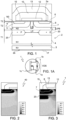
- a semiconductor power device is designated, as a whole, by the number 1, has a source terminal 1a, a drain terminal 1b and a gate terminal 1c and comprises a semiconductor body 2 of silicon carbide.
- the semiconductor body 2 comprises a substrate 3, a first epitaxial layer 4, formed on the substrate 3 and having a first thickness T1, and a second epitaxial layer 5, formed on the first epitaxial layer 4 and having a second thickness T2 smaller than the first thickness T1.
- the first thickness T1 is comprised in the range 10-30 ⁇ m
- the second thickness T2 is comprised in the range 0.8-2 ⁇ m.
- the first epitaxial layer 4 and the second epitaxial layer 5 both have a first conductivity type, for example of an N type.
- the first epitaxial layer 4 has, however, a first doping level N1 lower than a second doping level N2 of the second epitaxial layer.
- the first doping level N1 is in the order of 10 16 atoms/cm 3
- the second doping level N2 is in the order of 10 17 atoms/cm 3 .
- the semiconductor body 2 also comprises an enrichment layer 6, having a third thickness T3 smaller than the first thickness T1 and the second thickness T2 (for example 0.1 ⁇ m), the first conductivity type (N), and a third native doping level N3 higher than the first doping level N1 and the second doping level N2.
- the enrichment layer 6 may be a further epitaxial layer or may be obtained by implantation.
- the substrate 3 is of an N+ type and has a doping level, for example, in the order of 10 18 atoms/cm 3 .
- Body wells 7, having a second conductivity type, here of a P type, are formed within the second epitaxial layer 5 and house respective source regions 8, with the first conductivity type, in particular of an N+ type.
- the second epitaxial layer 5 defines a current spread layer (CSL), which extends to a greater depth from a first face 2a of the semiconductor body 2 as compared to the body wells 7, and the body wells 7 are embedded in the current spread layer.
- the second thickness T2 of the second epitaxial layer 5, which corresponds to the depth of the current spread layer is greater than the depth of the body wells 7 from the first face 2a.
- the body wells 7 are separated from one another by a body distance LB of less than 1 ⁇ m, for example 0.6 ⁇ m.
- the body wells 7 and the portion of the second epitaxial layer 5 comprised between them forms a parasitic-JFET region.
- a gate dielectric layer 10 extends on the first face 2a of the semiconductor body 2 over the second epitaxial layer 5 (or over the enrichment layer 6, if present) between the source regions 8 and is surmounted by a gate region 12.
- a source contact 13 extends over the source regions 8 and the gate region 12.
- An intermetal dielectric layer 15 insulates the gate region 12 from the source contact 13.
- a drain contact 17 is formed on a second face 2b of the semiconductor body 2 opposite to the first face 2a.
- the first epitaxial layer 4 houses floating protection pockets 20 having the second conductivity type, for example of a P+ type, with a doping level in the order of 10 18 atoms/cm 3 .
- the floating pockets 20 are shaped and arranged relative to the structures in the semiconductor body 2 so that the maximum intensity of the electrical field around the floating pockets 20 is greater than the maximum intensity of the electrical field around the body wells 7 at least for values of drain-to-source voltage VDS higher than a threshold voltage.
- the threshold voltage is less than a maximum nominal voltage, for example equal to 25%, or to 50% or to 65% of the maximum nominal voltage.
- the maximum nominal voltage is the maximum drain-source voltage at which a device, in particular the power device 1, may safely operate.
- the maximum nominal voltage is obviously lower than the breakdown voltage of power device 1 and is defined at design stage in accordance with the structural characteristics of the device and with the breakdown voltage.
- the floating pockets 20 are arranged underneath corresponding body wells 7 and are separated from one another by a protection distance LP greater than the body distance LB, for example, a difference between the protection distance LP and the body distance LB is comprised between 0.5 ⁇ m and 1.5 ⁇ m.
- a protection-to-body distance LPB between the floating pockets 20 and the corresponding body wells 7 in a direction perpendicular to the faces 2a and 2b of the semiconductor body 2 is less than 0.5 ⁇ m.
- the depth of the body wells 7 from the first face 2a of the semiconductor body 2 is at the most 0.5 ⁇ m less than the second thickness T2 of the second epitaxial layer 5.
- the power device 1 may be configured to operate with a gate-to-source voltage of 18 V, a maximum nominal voltage (maximum drain-to-source voltage VDS) beyond 1 kV, for example 1.2 kV or 3.3 kV, and currents of even several hundreds of amps or even higher.
- VDS maximum nominal voltage
- the floating pockets 20, as defined above, enable reduction of the intensity of the electrical field around the most critical regions, i.e., the junctions between the body wells 7 and the second epitaxial layer 5, where the combination with the particularly high current density is unfavourable, also due to the dimensions of the parasitic-JFET region.
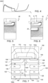
- FIGs 2 and 3 The situation of the electrical field is represented in Figures 2 and 3 directly and, furthermore, in Figures 5 and 6 through potential lines, respectively for a conventional power device 40 ( Figures 2 and 5 ) and for the power device 1 of Figure 1 ( Figures 3 and 6 ).
- the potential lines are particularly crowded around the body well and the values of electrical field are accordingly high.
- the potential lines are less crowded in the entire parasitic-JFET region and become more crowded around the floating pockets 20.
- the higher values of electrical field become deeper in the first epitaxial layer 4, where, however, the current density is markedly reduced because the region between the floating pockets 20 is much wider than the parasitic-JFET region.
- the time necessary for triggering the phenomena that lead in an uncontrolled way to short circuit due to excessive local heating, i.e., the short-circuit withstand time is advantageously increased, as illustrated in the graph of Figure 4 .
- the dashed line refers to a conventional power device, whereas the solid line refers to the power device 1 according to the invention.
- the effect of reduction of the electrical field in the critical regions around the body wells 7 and the corresponding increase of the short-circuit withstand time is also favoured by the protection-to-body distance LPB between the floating pockets 20 and the body wells 7.
- the protection-to-body distance LPB is in fact selected so that, at least for values of drain-to-source voltage VDS higher than the threshold voltage, the potential lines tend not to wrap around the body wells 7 and instead tend to stretch out towards the floating pockets 20, without penetrating or penetrating only marginally into the portion of the second epitaxial layer 5 comprised between the floating pockets 20 and the body wells 7. A greater distance would not allow stretching out of the potential lines and the corresponding reduction of the electrical field in the critical zones, in particular in the parasitic-JFET region.
- a further advantage is represented by the fact that the improvement of the short-circuit withstand time is made possible without altering significantly either the breakdown voltage or the ON-state drain-to-source resistance, normally denoted as R DSON . Rather, also an increase in the thickness of the current spread layer defined by the second epitaxial layer 5 in the order of 10-20% does not affect the breakdown voltage, which instead decreases in conventional power devices.
- a semiconductor power device 100 comprises a semiconductor body 102 of silicon carbide that includes, substantially as already described, a first epitaxial layer 104 and a second epitaxial layer 105, where body wells 107 and source regions 108 are formed.
- An enrichment layer 106 may be present on the surface of the semiconductor body 102.
- formed on a first face 102a of the semiconductor body 102 are a gate dielectric layer 110, a gate region 112, a source contact 113 and an intermetal dielectric layer 115.
- a drain contact 117 is formed on a second face 102b of the semiconductor body 102 opposite to the first face 102a.
- the semiconductor body 102 furthermore comprises an intermediate epitaxial layer 140, arranged between the first epitaxial layer 104 and the second epitaxial layer 105 and having a thickness TINT substantially equal to the thickness T2 of the second epitaxial layer 105 (for example, comprised in the range 0.8-2 ⁇ m).
- the doping levels diminish from the second epitaxial layer 105 (the highest, if an enrichment layer is not present, for example 10 17 atoms/cm 3 ), to the intermediate epitaxial layer 140 (which is intermediate also in doping, in addition to its position, for example 4 ⁇ 10 16 atoms/cm 3 ) and to the first epitaxial layer 104 (the lowest, for example 10 16 atoms/cm 3 ).
- the enrichment layer 106 is present, its doping level is the highest, for example 3 ⁇ 10 17 atoms/cm 3 .
- the first epitaxial layer 104 houses deep floating protection pockets 120 having the second conductivity type, for example of a P+ type with a doping level in the order of 10 18 atoms/cm 3 .
- the intermediate epitaxial layer 140 houses intermediate floating pockets 145 that are substantially the same as the deep floating pockets 120.
- the deep floating pockets 120 and the intermediate floating pockets 145 are shaped and arranged relative to the structures in the semiconductor body 102 so that the maximum intensity of the electrical field around the deep floating pockets 120 is greater than the maximum intensity of the electrical field around the body wells 107 at least for values of drain-to-source voltage VDS higher than a threshold voltage, which is less than a maximum nominal voltage.
- VDS drain-to-source voltage
- distances in a direction perpendicular to the faces 102a, 102b of the semiconductor body 102 between the deep floating pockets 120 and the intermediate floating pockets 145 and between the intermediate floating pockets 145 and the body wells 107 are less than 0.5 ⁇ m, for example 0.3 ⁇ m. These distances are not necessarily the same as one another.
- the number of levels of protection wells is not limited to two. In other embodiments, as in the semiconductor power device 200 of Figure 8 , in addition to the deep protection wells here designated by 220, there may be present, for example, two intermediate levels of protection wells 245, 246, or even a higher number, according to the design preferences.
- the intermediate floating pockets of each level are formed in respective intermediate epitaxial layers 240, 241.
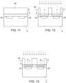
- the power device 1 of Figure 1 may be manufactured with the process described in the following with reference to Figures 9-13 .
- the first epitaxial layer 4 is formed for the desired thickness.
- a first mask layer 50 of TEOS TetraEthylOrthoSilicate
- the first mask layer 50 is then patterned ( Figure 10 ) to form a first implantation mask 51, which is then used for producing the floating pockets 20 by a first implantation P as far as the desired depth.
- the first implantation P in an embodiment is a multiple implantation in a number of steps, which enables a precise control of the implantation depth and of the shape of the floating pockets 20.
- the implanted dopant species may be aluminium, and the implantation may be performed in five steps, as defined in the table below.
- the second epitaxial layer 5 is grown, once again for the desired thickness ( Figure 11 ). If necessary, the enrichment layer 6 is formed through a further epitaxial growth or by surface implantation of dopant species.
- a second mask layer 55 is deposited and planarized, and then patterned to form a second implantation mask 56 ( Figure 12 ), which is used to produce the body wells 7 by a second implantation P as far as the desired depth. Also the second implantation may be a multiple implantation.
- the second implantation mask 56 is removed, and a third implantation mask 58 is formed ( Figure 13 ) from a mask layer (not illustrated entirely) with which the source regions 8 are formed.
- the third implantation mask 58 is removed, and the power device 1 is completed with the gate dielectric layer 10, the gate region 12, the intermetal dielectric layer 15, and the source contact 13, and finally by producing the source terminal 1a, the drain terminal 1b, and the gate terminal 1c ( Figure 1A ).
Landscapes
- Insulated Gate Type Field-Effect Transistor (AREA)
- Electrodes Of Semiconductors (AREA)
- Protection Of Static Devices (AREA)
Abstract
Description
- The present invention relates to a semiconductor power device with short circuit protection and to a process for manufacturing a semiconductor power device.
- It is known that, in semiconductor power devices, the tendency to reduce the dimensions to obtain high performance can expose to various conditions of risk that mainly involve certain parameters. A significant problem not only for conventional silicon power devices, but also for those based upon special materials like silicon carbide, is that of short circuit strength, often defined through the short-circuit withstand time. The current density within devices can reach extremely high values, in particular around structures like the junctions between the body wells and the drift region. Excessively high current densities may be the cause of intense local heating and even irreversible damage. For instance, heating may trigger phenomena of uncontrolled generation of electron-hole pairs ("thermal runaway"), which result in conditions of short circuit between drain regions and source regions and may not be stopped even by switching off the device. The short-circuit withstand time indicates how much a device is able to function in given conditions of current before a thermal short circuit occurs. The longer the short-circuit withstand time, the longer a device is able to function without suffering damage.
- Given that the problem is mainly linked to the current density and to the local dissipation of power, it is clear that the reduction of the dimensions (shrinkage) of the devices may have negative effects, unless the performance requirements are reduced. The reduction in dimensions encounters limits due to triggering of short circuits even in devices of silicon carbide, even though this has a thermal conductivity much higher than that of other semiconductor materials and is therefore able to dissipate the heat more efficiently.
- Various circuit solutions have been proposed to prevent or circumscribe potentially dangerous conditions. However, regardless of the effectiveness, they all lead to a significant increase in terms of cost and area occupied.
- The structural solutions aimed simply at reducing the ON-state drain-to-source resistance (normally denoted by RDSON) lead to limited benefits that, in any case, are not sufficient to increase in a satisfactory way the short-circuit withstand time.
- Consequently, as a whole the tendency to reduce the dimensions of power devices to obtain higher levels of performance is hindered by the problems due to the excessively high current density.
- The aim of the present invention is to provide a semiconductor power device and a process for manufacturing a semiconductor power device that will enable the limitations described to be overcome or at least mitigated.
- According to the present invention a semiconductor power device and a process for manufacturing a semiconductor power device are provided, as defined in
claims 1 and 14, respectively. - For a better understanding of the invention, some embodiments thereof will now be described, purely by way of non-limiting example and with reference to the attached drawings, wherein:
-
Figure 1 is a cross-sectional view through a semiconductor power device according to an embodiment of the present invention; -
Figure 1A is an equivalent electrical symbol of the power device ofFigure 1 ; -
Figures 2 and 3 are graphs relative to a distribution of intensity of electrical field in a known power device and in the power device ofFigure 1 , respectively; -
Figure 4 is a graph that shows short-circuit withstand times in a known power device and in the power device ofFigure 1 ; -
Figures 5 and 6 are graphs relative to a distribution of potential in a known power device and in the power device ofFigure 1 , respectively; -
Figure 7 is a cross-sectional view through a semiconductor power device according to a different embodiment of the present invention; -
Figure 8 is a cross-sectional view through a semiconductor power device according to a further embodiment of the present invention; and -
Figures 9-13 are cross-sectional views of a semiconductor wafer during successive steps of a process for manufacturing a semiconductor power device according to an embodiment of the present invention. - With reference to
Figures 1 and 1A , a semiconductor power device according to an embodiment of the present invention is designated, as a whole, by thenumber 1, has asource terminal 1a, adrain terminal 1b and agate terminal 1c and comprises asemiconductor body 2 of silicon carbide. Thesemiconductor body 2, in turn, comprises asubstrate 3, a firstepitaxial layer 4, formed on thesubstrate 3 and having a first thickness T1, and a secondepitaxial layer 5, formed on the firstepitaxial layer 4 and having a second thickness T2 smaller than the first thickness T1. For instance, the first thickness T1 is comprised in the range 10-30 µm, and the second thickness T2 is comprised in the range 0.8-2 µm. The firstepitaxial layer 4 and the secondepitaxial layer 5 both have a first conductivity type, for example of an N type. The firstepitaxial layer 4 has, however, a first doping level N1 lower than a second doping level N2 of the second epitaxial layer. For instance, the first doping level N1 is in the order of 1016 atoms/cm3, whereas the second doping level N2 is in the order of 1017 atoms/cm3. In an embodiment, thesemiconductor body 2 also comprises anenrichment layer 6, having a third thickness T3 smaller than the first thickness T1 and the second thickness T2 (for example 0.1 µm), the first conductivity type (N), and a third native doping level N3 higher than the first doping level N1 and the second doping level N2. Theenrichment layer 6 may be a further epitaxial layer or may be obtained by implantation. Thesubstrate 3 is of an N+ type and has a doping level, for example, in the order of 1018 atoms/cm3. -
Body wells 7, having a second conductivity type, here of a P type, are formed within the secondepitaxial layer 5 and houserespective source regions 8, with the first conductivity type, in particular of an N+ type. The secondepitaxial layer 5 defines a current spread layer (CSL), which extends to a greater depth from afirst face 2a of thesemiconductor body 2 as compared to thebody wells 7, and thebody wells 7 are embedded in the current spread layer. In other words, the second thickness T2 of the secondepitaxial layer 5, which corresponds to the depth of the current spread layer, is greater than the depth of thebody wells 7 from thefirst face 2a. - The
body wells 7 are separated from one another by a body distance LB of less than 1 µm, for example 0.6 µm. Thebody wells 7 and the portion of the secondepitaxial layer 5 comprised between them forms a parasitic-JFET region. A gatedielectric layer 10 extends on thefirst face 2a of thesemiconductor body 2 over the second epitaxial layer 5 (or over theenrichment layer 6, if present) between thesource regions 8 and is surmounted by agate region 12. Asource contact 13 extends over thesource regions 8 and thegate region 12. An intermetaldielectric layer 15 insulates thegate region 12 from thesource contact 13. Adrain contact 17 is formed on asecond face 2b of thesemiconductor body 2 opposite to thefirst face 2a. - At an interface with the overlying epitaxial layer, i.e., the second
epitaxial layer 5, the firstepitaxial layer 4 houses floatingprotection pockets 20 having the second conductivity type, for example of a P+ type, with a doping level in the order of 1018 atoms/cm3. Furthermore, the floatingpockets 20 are shaped and arranged relative to the structures in thesemiconductor body 2 so that the maximum intensity of the electrical field around the floatingpockets 20 is greater than the maximum intensity of the electrical field around thebody wells 7 at least for values of drain-to-source voltage VDS higher than a threshold voltage. The threshold voltage is less than a maximum nominal voltage, for example equal to 25%, or to 50% or to 65% of the maximum nominal voltage. The maximum nominal voltage is the maximum drain-source voltage at which a device, in particular thepower device 1, may safely operate. The maximum nominal voltage is obviously lower than the breakdown voltage ofpower device 1 and is defined at design stage in accordance with the structural characteristics of the device and with the breakdown voltage. The floatingpockets 20 are arranged underneathcorresponding body wells 7 and are separated from one another by a protection distance LP greater than the body distance LB, for example, a difference between the protection distance LP and the body distance LB is comprised between 0.5 µm and 1.5 µm. A protection-to-body distance LPB between thefloating pockets 20 and thecorresponding body wells 7 in a direction perpendicular to thefaces semiconductor body 2 is less than 0.5 µm. In practice, the depth of thebody wells 7 from thefirst face 2a of thesemiconductor body 2 is at the most 0.5 µm less than the second thickness T2 of the secondepitaxial layer 5. +++ - The
power device 1 may be configured to operate with a gate-to-source voltage of 18 V, a maximum nominal voltage (maximum drain-to-source voltage VDS) beyond 1 kV, for example 1.2 kV or 3.3 kV, and currents of even several hundreds of amps or even higher. Thefloating pockets 20, as defined above, enable reduction of the intensity of the electrical field around the most critical regions, i.e., the junctions between thebody wells 7 and the secondepitaxial layer 5, where the combination with the particularly high current density is unfavourable, also due to the dimensions of the parasitic-JFET region. The situation of the electrical field is represented inFigures 2 and 3 directly and, furthermore, inFigures 5 and 6 through potential lines, respectively for a conventional power device 40 (Figures 2 and5 ) and for thepower device 1 ofFigure 1 (Figures 3 and6 ). As may be noted, in the conventional power device, the potential lines are particularly crowded around the body well and the values of electrical field are accordingly high. In thepower device 1, instead, above the threshold voltage and in conditions of conduction the potential lines are less crowded in the entire parasitic-JFET region and become more crowded around thefloating pockets 20. In practice, then, the higher values of electrical field become deeper in the firstepitaxial layer 4, where, however, the current density is markedly reduced because the region between thefloating pockets 20 is much wider than the parasitic-JFET region. In this way, the time necessary for triggering the phenomena that lead in an uncontrolled way to short circuit due to excessive local heating, i.e., the short-circuit withstand time, is advantageously increased, as illustrated in the graph ofFigure 4 . Here, the dashed line refers to a conventional power device, whereas the solid line refers to thepower device 1 according to the invention. - The effect of reduction of the electrical field in the critical regions around the
body wells 7 and the corresponding increase of the short-circuit withstand time is also favoured by the protection-to-body distance LPB between the floatingpockets 20 and thebody wells 7. The protection-to-body distance LPB is in fact selected so that, at least for values of drain-to-source voltage VDS higher than the threshold voltage, the potential lines tend not to wrap around thebody wells 7 and instead tend to stretch out towards the floatingpockets 20, without penetrating or penetrating only marginally into the portion of thesecond epitaxial layer 5 comprised between the floatingpockets 20 and thebody wells 7. A greater distance would not allow stretching out of the potential lines and the corresponding reduction of the electrical field in the critical zones, in particular in the parasitic-JFET region. - A further advantage is represented by the fact that the improvement of the short-circuit withstand time is made possible without altering significantly either the breakdown voltage or the ON-state drain-to-source resistance, normally denoted as RDSON. Rather, also an increase in the thickness of the current spread layer defined by the
second epitaxial layer 5 in the order of 10-20% does not affect the breakdown voltage, which instead decreases in conventional power devices. - With reference to
Figure 7 , in an embodiment asemiconductor power device 100 comprises asemiconductor body 102 of silicon carbide that includes, substantially as already described, afirst epitaxial layer 104 and asecond epitaxial layer 105, wherebody wells 107 andsource regions 108 are formed. Anenrichment layer 106 may be present on the surface of thesemiconductor body 102. As in the embodiment ofFigure 1 , formed on afirst face 102a of thesemiconductor body 102 are agate dielectric layer 110, agate region 112, asource contact 113 and anintermetal dielectric layer 115. Adrain contact 117 is formed on asecond face 102b of thesemiconductor body 102 opposite to thefirst face 102a. - The
semiconductor body 102 furthermore comprises anintermediate epitaxial layer 140, arranged between thefirst epitaxial layer 104 and thesecond epitaxial layer 105 and having a thickness TINT substantially equal to the thickness T2 of the second epitaxial layer 105 (for example, comprised in the range 0.8-2 µm). - The doping levels diminish from the second epitaxial layer 105 (the highest, if an enrichment layer is not present, for example 1017 atoms/cm3), to the intermediate epitaxial layer 140 (which is intermediate also in doping, in addition to its position, for example 4 × 10¹⁶ atoms/cm3) and to the first epitaxial layer 104 (the lowest, for example 1016 atoms/cm3). In the case where the
enrichment layer 106 is present, its doping level is the highest, for example 3 × 10¹⁷ atoms/cm3. - At an interface with the overlying epitaxial layer, in this case the
intermediate epitaxial layer 140, thefirst epitaxial layer 104 houses deep floating protection pockets 120 having the second conductivity type, for example of a P+ type with a doping level in the order of 1018 atoms/cm3. - At an interface with the
second epitaxial layer 105, theintermediate epitaxial layer 140 houses intermediate floatingpockets 145 that are substantially the same as the deep floatingpockets 120. - The deep floating
pockets 120 and the intermediate floatingpockets 145 are shaped and arranged relative to the structures in thesemiconductor body 102 so that the maximum intensity of the electrical field around the deep floatingpockets 120 is greater than the maximum intensity of the electrical field around thebody wells 107 at least for values of drain-to-source voltage VDS higher than a threshold voltage, which is less than a maximum nominal voltage. In particular, distances in a direction perpendicular to thefaces semiconductor body 102 between the deep floatingpockets 120 and the intermediate floatingpockets 145 and between the intermediate floatingpockets 145 and thebody wells 107 are less than 0.5 µm, for example 0.3 µm. These distances are not necessarily the same as one another. - The presence of protection wells on a number of levels enables amplification of the effect of translation of the high values of electrical field towards the inside of the
semiconductor body 102, at a greater distance from thefirst face 102a. - The number of levels of protection wells is not limited to two. In other embodiments, as in the
semiconductor power device 200 ofFigure 8 , in addition to the deep protection wells here designated by 220, there may be present, for example, two intermediate levels ofprotection wells epitaxial layers - The
power device 1 ofFigure 1 may be manufactured with the process described in the following with reference toFigures 9-13 . Initially, thefirst epitaxial layer 4 is formed for the desired thickness. Then, afirst mask layer 50 of TEOS (TetraEthylOrthoSilicate) is deposited and planarized. - The
first mask layer 50 is then patterned (Figure 10 ) to form afirst implantation mask 51, which is then used for producing the floatingpockets 20 by a first implantation P as far as the desired depth. The first implantation P in an embodiment is a multiple implantation in a number of steps, which enables a precise control of the implantation depth and of the shape of the floating pockets 20. The implanted dopant species may be aluminium, and the implantation may be performed in five steps, as defined in the table below.Dopant species Concentration [atoms/cm3] Implantation energy [keV] Al + 1012 30 Al + 1012 80 Al + 1013 160 Al ++ 3.12 × 10¹³ 300 Al ++ 5.20 × 10¹³ 400 - After removal of the
first implantation mask 1, thesecond epitaxial layer 5 is grown, once again for the desired thickness (Figure 11 ). If necessary, theenrichment layer 6 is formed through a further epitaxial growth or by surface implantation of dopant species. - A
second mask layer 55 is deposited and planarized, and then patterned to form a second implantation mask 56 (Figure 12 ), which is used to produce thebody wells 7 by a second implantation P as far as the desired depth. Also the second implantation may be a multiple implantation. - The
second implantation mask 56 is removed, and athird implantation mask 58 is formed (Figure 13 ) from a mask layer (not illustrated entirely) with which thesource regions 8 are formed. - The
third implantation mask 58 is removed, and thepower device 1 is completed with thegate dielectric layer 10, thegate region 12, theintermetal dielectric layer 15, and thesource contact 13, and finally by producing thesource terminal 1a, thedrain terminal 1b, and thegate terminal 1c (Figure 1A ). - Finally, it is clear that modifications and variations may be made to the device and to the process described herein, without thereby departing from the scope of the present invention, as defined in the annexed claims.
Claims (16)
- A semiconductor power device having a maximum nominal voltage and comprising:a semiconductor body (2; 102) containing silicon carbide and having a first conductivity type;a first conduction terminal (1a) on a first face (2a; 102a) of the semiconductor body (2; 102) and a second conduction terminal (1b) on a second face (2b; 102b) of the semiconductor body (2; 102);body wells (7; 107) having a second conductivity type, housed in the semiconductor body and separated from one another by a body distance (LB);source regions housed in the body wells (7) and connected to the first conduction terminal (1a);a control region (12) extending on the semiconductor body (2; 102) between the source regions (8; 108); andfloating pockets (20; 120) having the second conductivity type, formed in the semiconductor body (2; 102) at a distance from the body wells (7; 107) between the first face (2a; 102a) and the second face (2b; 102b) of the semiconductor body (2; 102);wherein the floating pockets (20; 120) are shaped and arranged relative to the body wells (7; 107) so that a maximum intensity of electrical field around the floating pockets (20; 120) is greater than a maximum intensity of electrical field around the body wells (7; 107) at least for values of an operating voltage (VDS) between the first conduction terminal (1a) and the second conduction terminal (1b) higher than a threshold voltage, the threshold voltage being less than the maximum nominal voltage.
- The device according to claim 1, wherein:the semiconductor body (2; 102) comprises a first epitaxial layer (4; 104), having the first conductivity type and a first doping level (N1), and a second epitaxial layer (5; 105), having the first conductivity type and a second doping level (N2), higher than the first doping level (N1);the body wells (7; 107) are housed in the second epitaxial layer (5; 105); andthe floating pockets (20; 120) are housed in the first epitaxial layer (4; 104).
- The device according to claim 2, wherein the floating pockets (20; 120) are housed at an interface of the first epitaxial layer (4; 104) with an epitaxial layer overlying the first epitaxial layer (4; 104).
- The device according to claim 3, wherein the epitaxial layer overlying the first epitaxial layer (4) is the second epitaxial layer (5).
- The device according to claim 4, wherein a protection-to-body distance (LPB) between the floating pockets (20) and the corresponding body wells (7) in a direction perpendicular to the first face (2a) and to the second face (2b) of the semiconductor body (2) is less than 0.5 µm.
- The device according to claim 3, wherein the semiconductor body (102) comprises an intermediate epitaxial layer (140), arranged between the first epitaxial layer (104) and the second epitaxial layer (105) and having a doping level intermediate between the first doping level (N1) and the second doping level (N2), and wherein the epitaxial layer overlying the first epitaxial layer (104) is the intermediate epitaxial layer (140).
- The device according to claim 6, comprising intermediate floating pockets (145) having the second conductivity type, formed in the intermediate epitaxial layer (140) at an interface with the second epitaxial layer (105) .
- The device according to claim 6 or claim 7, wherein distances in a direction perpendicular to the first face (102a) and to the second face (102b) of the semiconductor body (102) between the floating pockets (120) and the intermediate floating pockets (145) and between the intermediate floating pockets (145) and the body wells (107) are less than 0.5 µm.
- The device according to any one of claims 2 to 8, wherein the semiconductor body (2; 102) comprises a surface enrichment layer (6; 106), having a third native doping level (N3) higher than the first doping level (N1) and the second doping level (N2) and wherein the first epitaxial layer (104) has a first thickness (T1), the second epitaxial layer (105) has a second thickness (T2), and the enrichment layer (6; 106) has a third thickness (T3) smaller than the first thickness (T1) and the second thickness (T2).
- The device according to any one of the preceding claims, wherein the body wells (7; 107) are separated from one another by a body distance (LB) and wherein the floating pockets (20; 120) are arranged underneath corresponding body wells (7; 107) and are separated from one another by a protection distance (LP) greater than the body distance (LB), for example by an amount comprised between 0.5 µm and 1.5 µm.
- The device according to any one of the preceding claims, wherein the body distance (LB) is less than 1 µm, for example 0.6 µm.
- The device according to any one of the preceding claims, wherein the second epitaxial layer (5; 105) defines a current spread layer, which extends up to a greater depth from the first face (2a; 102a) of the semiconductor body (2; 102) than the body wells (7; 107).
- The device according to any one of the preceding claims, wherein the floating pockets (20; 120) have the second conductivity type and a doping level in the order of 1018 atoms/cm3.
- A process for manufacturing a semiconductor power device comprising:forming a semiconductor body (2; 102) containing silicon carbide and having a first conductivity type (N);forming body wells (7; 107) having a second conductivity type (P), housed in the semiconductor body and separated from one another by a body distance (LB);forming source regions (8) having the first conductivity type (N) and housed in the body wells (7); andforming floating pockets (20; 120) having the second conductivity type in the semiconductor body (2; 102) at a distance from the body wells (7; 107) between a first face (2a; 102a) and a second face (2b; 102b) of the semiconductor body (2; 102);forming a first conduction terminal (1a) connected to the source regions (8) on the first face (2a; 102a) of the semiconductor body (2; 102) and a second conduction terminal (1b) on the second face (2b; 102b) of the semiconductor body (2; 102); andforming a control region (12) extending on the semiconductor body (2; 102) between the source regions (8; 108) ;wherein the floating pockets (20; 120) are shaped and arranged relative to the body wells (7; 107) so that a maximum intensity of electrical field around the floating pockets (20; 120) is greater than a maximum intensity of electrical field around the body wells (7; 107) at least for values of an operating voltage (VDS) between the first conduction terminal (1a) and the second conduction terminal (1b) greater than a threshold voltage, the threshold voltage being less than a maximum nominal voltage.
- The process according to claim 14, wherein forming the semiconductor body (2; 102) comprises forming a first epitaxial layer (4; 104), having the first conductivity type and a first doping level (N1), and a second epitaxial layer (5; 105), having the first conductivity type and a second doping level (N2) higher than the first doping level (N1); and wherein the floating pockets (20; 120) are formed in the first epitaxial layer (4; 104) and the body wells (7; 107) are formed in the second epitaxial layer (5; 105).
- The process according to claim 15, wherein forming floating pockets (20) comprises forming a first implantation mask (51) on the first epitaxial layer (4) and carrying out a first implantation, for example a first multiple implantation, of a dopant species of the second type using the first implantation mask (51); and wherein forming body wells (7) comprises forming a second implantation mask (56) and carrying out a second implantation, for example a second multiple implantation, of a dopant species of the second type using the second implantation mask (56).
Applications Claiming Priority (1)
| Application Number | Priority Date | Filing Date | Title |
|---|---|---|---|
| IT102021000027842A IT202100027842A1 (en) | 2021-10-29 | 2021-10-29 | SEMICONDUCTOR POWER DEVICE WITH SHORT CIRCUIT PROTECTION AND METHOD FOR MANUFACTUREING A SEMICONDUCTOR POWER DEVICE |
Publications (3)
| Publication Number | Publication Date |
|---|---|
| EP4177960A1 true EP4177960A1 (en) | 2023-05-10 |
| EP4177960B1 EP4177960B1 (en) | 2025-12-17 |
| EP4177960C0 EP4177960C0 (en) | 2025-12-17 |
Family
ID=79164472
Family Applications (1)
| Application Number | Title | Priority Date | Filing Date |
|---|---|---|---|
| EP22204133.7A Active EP4177960B1 (en) | 2021-10-29 | 2022-10-27 | Semiconductor power device with short circuit protection and process for manufacturing a semiconductor power device |
Country Status (5)
| Country | Link |
|---|---|
| US (1) | US20230134850A1 (en) |
| EP (1) | EP4177960B1 (en) |
| JP (1) | JP2023067790A (en) |
| CN (2) | CN116072728A (en) |
| IT (1) | IT202100027842A1 (en) |
Families Citing this family (3)
| Publication number | Priority date | Publication date | Assignee | Title |
|---|---|---|---|---|
| IT202100027842A1 (en) * | 2021-10-29 | 2023-04-29 | St Microelectronics Srl | SEMICONDUCTOR POWER DEVICE WITH SHORT CIRCUIT PROTECTION AND METHOD FOR MANUFACTUREING A SEMICONDUCTOR POWER DEVICE |
| CN119584613A (en) * | 2025-02-06 | 2025-03-07 | 华通芯电(南昌)电子科技有限公司 | A SiC MOSFET device and preparation method thereof |
| TWI900409B (en) * | 2025-02-12 | 2025-10-01 | 李羿軒 | Vertical power semiconductor device |
Citations (4)
| Publication number | Priority date | Publication date | Assignee | Title |
|---|---|---|---|---|
| US6573534B1 (en) * | 1995-09-06 | 2003-06-03 | Denso Corporation | Silicon carbide semiconductor device |
| JP2015115375A (en) * | 2013-12-09 | 2015-06-22 | 国立研究開発法人産業技術総合研究所 | Silicon carbide semiconductor device |
| CN111725318A (en) * | 2020-06-18 | 2020-09-29 | 湖南国芯半导体科技有限公司 | Cell structure of a power semiconductor device and method of making the same |
| US11152503B1 (en) * | 2019-11-05 | 2021-10-19 | Semiq Incorporated | Silicon carbide MOSFET with wave-shaped channel regions |
Family Cites Families (4)
| Publication number | Priority date | Publication date | Assignee | Title |
|---|---|---|---|---|
| JP4746169B2 (en) * | 2000-04-28 | 2011-08-10 | 株式会社東芝 | Power semiconductor device and driving method thereof |
| KR101367491B1 (en) * | 2012-08-08 | 2014-02-26 | 고려대학교 산학협력단 | Method for manufacturing semiconductor device having a single floating island and semiconductor device manufactured thereby |
| WO2021137341A1 (en) * | 2020-01-03 | 2021-07-08 | 엘지전자 주식회사 | Metal-oxide-semiconductor field-effect transistor device, and manufacturing method therefor |
| IT202100027842A1 (en) * | 2021-10-29 | 2023-04-29 | St Microelectronics Srl | SEMICONDUCTOR POWER DEVICE WITH SHORT CIRCUIT PROTECTION AND METHOD FOR MANUFACTUREING A SEMICONDUCTOR POWER DEVICE |
-
2021
- 2021-10-29 IT IT102021000027842A patent/IT202100027842A1/en unknown
-
2022
- 2022-10-11 US US18/045,784 patent/US20230134850A1/en active Pending
- 2022-10-19 JP JP2022167881A patent/JP2023067790A/en active Pending
- 2022-10-27 EP EP22204133.7A patent/EP4177960B1/en active Active
- 2022-10-28 CN CN202211335559.0A patent/CN116072728A/en active Pending
- 2022-10-28 CN CN202222860322.6U patent/CN220341228U/en active Active
Patent Citations (4)
| Publication number | Priority date | Publication date | Assignee | Title |
|---|---|---|---|---|
| US6573534B1 (en) * | 1995-09-06 | 2003-06-03 | Denso Corporation | Silicon carbide semiconductor device |
| JP2015115375A (en) * | 2013-12-09 | 2015-06-22 | 国立研究開発法人産業技術総合研究所 | Silicon carbide semiconductor device |
| US11152503B1 (en) * | 2019-11-05 | 2021-10-19 | Semiq Incorporated | Silicon carbide MOSFET with wave-shaped channel regions |
| CN111725318A (en) * | 2020-06-18 | 2020-09-29 | 湖南国芯半导体科技有限公司 | Cell structure of a power semiconductor device and method of making the same |
Non-Patent Citations (2)
| Title |
|---|
| CEZAC N ET AL: "A NEW GENERATION OF POWER UNIPOLAR DEVICESD THE CONCEPT OF THE FLOATING ISLANDS MOS TRANSISTOR (FLIMOST)", 12TH. INTERNATIONAL SYMPOSIUM ON POWER SEMICONDUCTOR DEVICES AND IC S. ISPSD 2000. PROCEEDINGS. TOULOUSE, FRANCE, MAY 22 - 25, 2000; [INTERNATIONAL SYMPOSIUM ON POWER SEMICONDUCTOR DEVICES & IC'S], NEW YORK, NY : IEEE, US, 22 May 2000 (2000-05-22), pages 69 - 72, XP000987835, ISBN: 978-0-7803-6269-7, DOI: 10.1109/ISPSD.2000.856775 * |
| LUO HOU-CAI ET AL: "Investigations of SiC VDMOSFET With Floating Island Structure Based on TCAD", IEEE TRANSACTIONS ON ELECTRON DEVICES, IEEE, USA, vol. 66, no. 5, 31 May 2019 (2019-05-31), pages 2295 - 2300, XP011720496, ISSN: 0018-9383, [retrieved on 20190419], DOI: 10.1109/TED.2019.2900384 * |
Also Published As
| Publication number | Publication date |
|---|---|
| CN116072728A (en) | 2023-05-05 |
| CN220341228U (en) | 2024-01-12 |
| IT202100027842A1 (en) | 2023-04-29 |
| US20230134850A1 (en) | 2023-05-04 |
| JP2023067790A (en) | 2023-05-16 |
| EP4177960B1 (en) | 2025-12-17 |
| EP4177960C0 (en) | 2025-12-17 |
Similar Documents
| Publication | Publication Date | Title |
|---|---|---|
| EP4177960B1 (en) | Semiconductor power device with short circuit protection and process for manufacturing a semiconductor power device | |
| US5973359A (en) | MOS type semiconductor device | |
| US6586798B1 (en) | High voltage MOS-gated power device | |
| US7125777B2 (en) | Asymmetric hetero-doped high-voltage MOSFET (AH2MOS) | |
| US11049962B2 (en) | Silicon carbide power devices | |
| KR20190068627A (en) | Power semiconductor devices and associated methods having gate trenches with implanted sidewalls | |
| US20230411446A1 (en) | Gate trench power semiconductor devices having trench shielding patterns formed during the well implant and related methods | |
| SE542607C2 (en) | MOSFET in SiC with self-aligned lateral MOS channel | |
| JP2011129547A (en) | Semiconductor device and method of manufacturing the same | |
| US20090283796A1 (en) | Semiconductor device and method for forming the same | |
| US5952699A (en) | Insulated gate semiconductor device and method of manufacturing the same | |
| JP7584630B2 (en) | Power silicon carbide-based semiconductor device with improved short circuit capability and method for making such device - Patents.com | |
| US20050006701A1 (en) | High voltage metal-oxide semiconductor device | |
| US10516017B2 (en) | Semiconductor device, and manufacturing method for same | |
| US11721755B2 (en) | Methods of forming semiconductor power devices having graded lateral doping | |
| CN113035931A (en) | Trench MOSFET device and method of manufacturing the same | |
| US20250169128A1 (en) | Gate trench power semiconductor devices with deep jfet patterns | |
| US7663203B2 (en) | High-voltage PMOS transistor | |
| KR20210009005A (en) | Semiconductor device and method manufacturing the same | |
| US20240234495A1 (en) | Gate trench power semiconductor devices having self-aligned trench shielding regions and related methods | |
| KR101216851B1 (en) | Semiconductor device and method of manufacturing the same | |
| CN207021266U (en) | A kind of high-power planar grid D MOSFET structures | |
| US12396219B2 (en) | Metal-oxide film semiconductor field-effect transistor device and method for manufacturing same | |
| KR102917097B1 (en) | SiC TRENCH MOSFET AND METHOD FOR MANUFACTURING THE SAME | |
| KR102319595B1 (en) | Semiconductor Device And Methods For Manufacturing Of The Same |
Legal Events
| Date | Code | Title | Description |
|---|---|---|---|
| PUAI | Public reference made under article 153(3) epc to a published international application that has entered the european phase |
Free format text: ORIGINAL CODE: 0009012 |
|
| STAA | Information on the status of an ep patent application or granted ep patent |
Free format text: STATUS: THE APPLICATION HAS BEEN PUBLISHED |
|
| AK | Designated contracting states |
Kind code of ref document: A1 Designated state(s): AL AT BE BG CH CY CZ DE DK EE ES FI FR GB GR HR HU IE IS IT LI LT LU LV MC ME MK MT NL NO PL PT RO RS SE SI SK SM TR |
|
| STAA | Information on the status of an ep patent application or granted ep patent |
Free format text: STATUS: REQUEST FOR EXAMINATION WAS MADE |
|
| 17P | Request for examination filed |
Effective date: 20231110 |
|
| RBV | Designated contracting states (corrected) |
Designated state(s): AL AT BE BG CH CY CZ DE DK EE ES FI FR GB GR HR HU IE IS IT LI LT LU LV MC ME MK MT NL NO PL PT RO RS SE SI SK SM TR |
|
| REG | Reference to a national code |
Ref country code: DE Ref legal event code: R079 Free format text: PREVIOUS MAIN CLASS: H01L0029780000 Ipc: H10D0030010000 Ref country code: DE Ref legal event code: R079 Ref document number: 602022026940 Country of ref document: DE Free format text: PREVIOUS MAIN CLASS: H01L0029780000 Ipc: H10D0030010000 |
|
| GRAP | Despatch of communication of intention to grant a patent |
Free format text: ORIGINAL CODE: EPIDOSNIGR1 |
|
| STAA | Information on the status of an ep patent application or granted ep patent |
Free format text: STATUS: GRANT OF PATENT IS INTENDED |
|
| RIC1 | Information provided on ipc code assigned before grant |
Ipc: H10D 62/10 20250101ALI20250213BHEP Ipc: H10D 30/66 20250101ALI20250213BHEP Ipc: H10D 30/01 20250101AFI20250213BHEP |
|
| INTG | Intention to grant announced |
Effective date: 20250224 |
|
| GRAJ | Information related to disapproval of communication of intention to grant by the applicant or resumption of examination proceedings by the epo deleted |
Free format text: ORIGINAL CODE: EPIDOSDIGR1 |
|
| STAA | Information on the status of an ep patent application or granted ep patent |
Free format text: STATUS: REQUEST FOR EXAMINATION WAS MADE |
|
| GRAP | Despatch of communication of intention to grant a patent |
Free format text: ORIGINAL CODE: EPIDOSNIGR1 |
|
| STAA | Information on the status of an ep patent application or granted ep patent |
Free format text: STATUS: GRANT OF PATENT IS INTENDED |
|
| INTC | Intention to grant announced (deleted) | ||
| INTG | Intention to grant announced |
Effective date: 20250715 |
|
| GRAS | Grant fee paid |
Free format text: ORIGINAL CODE: EPIDOSNIGR3 |
|
| GRAA | (expected) grant |
Free format text: ORIGINAL CODE: 0009210 |
|
| STAA | Information on the status of an ep patent application or granted ep patent |
Free format text: STATUS: THE PATENT HAS BEEN GRANTED |
|
| AK | Designated contracting states |
Kind code of ref document: B1 Designated state(s): AL AT BE BG CH CY CZ DE DK EE ES FI FR GB GR HR HU IE IS IT LI LT LU LV MC ME MK MT NL NO PL PT RO RS SE SI SK SM TR |
|
| REG | Reference to a national code |
Ref country code: CH Ref legal event code: F10 Free format text: ST27 STATUS EVENT CODE: U-0-0-F10-F00 (AS PROVIDED BY THE NATIONAL OFFICE) Effective date: 20251217 Ref country code: GB Ref legal event code: FG4D |
|
| REG | Reference to a national code |
Ref country code: DE Ref legal event code: R096 Ref document number: 602022026940 Country of ref document: DE |
|
| U01 | Request for unitary effect filed |
Effective date: 20251219 |
|
| U07 | Unitary effect registered |
Designated state(s): AT BE BG DE DK EE FI FR IT LT LU LV MT NL PT RO SE SI Effective date: 20260105 |
|
| PG25 | Lapsed in a contracting state [announced via postgrant information from national office to epo] |
Ref country code: NO Free format text: LAPSE BECAUSE OF FAILURE TO SUBMIT A TRANSLATION OF THE DESCRIPTION OR TO PAY THE FEE WITHIN THE PRESCRIBED TIME-LIMIT Effective date: 20260317 |
|
| PG25 | Lapsed in a contracting state [announced via postgrant information from national office to epo] |
Ref country code: HR Free format text: LAPSE BECAUSE OF FAILURE TO SUBMIT A TRANSLATION OF THE DESCRIPTION OR TO PAY THE FEE WITHIN THE PRESCRIBED TIME-LIMIT Effective date: 20251217 |
|
| PG25 | Lapsed in a contracting state [announced via postgrant information from national office to epo] |
Ref country code: RS Free format text: LAPSE BECAUSE OF FAILURE TO SUBMIT A TRANSLATION OF THE DESCRIPTION OR TO PAY THE FEE WITHIN THE PRESCRIBED TIME-LIMIT Effective date: 20260317 |