EP4177939A2 - System in a package (sip) with air cavity - Google Patents
System in a package (sip) with air cavity Download PDFInfo
- Publication number
- EP4177939A2 EP4177939A2 EP22205106.2A EP22205106A EP4177939A2 EP 4177939 A2 EP4177939 A2 EP 4177939A2 EP 22205106 A EP22205106 A EP 22205106A EP 4177939 A2 EP4177939 A2 EP 4177939A2
- Authority
- EP
- European Patent Office
- Prior art keywords
- sip
- lid
- substrate
- ring
- metal
- Prior art date
- Legal status (The legal status is an assumption and is not a legal conclusion. Google has not performed a legal analysis and makes no representation as to the accuracy of the status listed.)
- Pending
Links
Images




Classifications
-
- H—ELECTRICITY
- H10—SEMICONDUCTOR DEVICES; ELECTRIC SOLID-STATE DEVICES NOT OTHERWISE PROVIDED FOR
- H10W—GENERIC PACKAGES, INTERCONNECTIONS, CONNECTORS OR OTHER CONSTRUCTIONAL DETAILS OF DEVICES COVERED BY CLASS H10
- H10W76/00—Containers; Fillings or auxiliary members therefor; Seals
- H10W76/10—Containers or parts thereof
- H10W76/12—Containers or parts thereof characterised by their shape
-
- H—ELECTRICITY
- H10—SEMICONDUCTOR DEVICES; ELECTRIC SOLID-STATE DEVICES NOT OTHERWISE PROVIDED FOR
- H10W—GENERIC PACKAGES, INTERCONNECTIONS, CONNECTORS OR OTHER CONSTRUCTIONAL DETAILS OF DEVICES COVERED BY CLASS H10
- H10W76/00—Containers; Fillings or auxiliary members therefor; Seals
- H10W76/60—Seals
-
- H—ELECTRICITY
- H10—SEMICONDUCTOR DEVICES; ELECTRIC SOLID-STATE DEVICES NOT OTHERWISE PROVIDED FOR
- H10W—GENERIC PACKAGES, INTERCONNECTIONS, CONNECTORS OR OTHER CONSTRUCTIONAL DETAILS OF DEVICES COVERED BY CLASS H10
- H10W42/00—Arrangements for protection of devices
-
- H—ELECTRICITY
- H10—SEMICONDUCTOR DEVICES; ELECTRIC SOLID-STATE DEVICES NOT OTHERWISE PROVIDED FOR
- H10W—GENERIC PACKAGES, INTERCONNECTIONS, CONNECTORS OR OTHER CONSTRUCTIONAL DETAILS OF DEVICES COVERED BY CLASS H10
- H10W42/00—Arrangements for protection of devices
- H10W42/20—Arrangements for protection of devices protecting against electromagnetic or particle radiation, e.g. light, X-rays, gamma-rays or electrons
- H10W42/261—Arrangements for protection of devices protecting against electromagnetic or particle radiation, e.g. light, X-rays, gamma-rays or electrons characterised by their shapes or dispositions
- H10W42/273—Arrangements for protection of devices protecting against electromagnetic or particle radiation, e.g. light, X-rays, gamma-rays or electrons characterised by their shapes or dispositions the arrangements being between laterally adjacent chips, e.g. walls between chips
-
- H—ELECTRICITY
- H10—SEMICONDUCTOR DEVICES; ELECTRIC SOLID-STATE DEVICES NOT OTHERWISE PROVIDED FOR
- H10W—GENERIC PACKAGES, INTERCONNECTIONS, CONNECTORS OR OTHER CONSTRUCTIONAL DETAILS OF DEVICES COVERED BY CLASS H10
- H10W76/00—Containers; Fillings or auxiliary members therefor; Seals
- H10W76/10—Containers or parts thereof
- H10W76/12—Containers or parts thereof characterised by their shape
- H10W76/15—Containers comprising an insulating or insulated base
-
- H—ELECTRICITY
- H10—SEMICONDUCTOR DEVICES; ELECTRIC SOLID-STATE DEVICES NOT OTHERWISE PROVIDED FOR
- H10W—GENERIC PACKAGES, INTERCONNECTIONS, CONNECTORS OR OTHER CONSTRUCTIONAL DETAILS OF DEVICES COVERED BY CLASS H10
- H10W76/00—Containers; Fillings or auxiliary members therefor; Seals
- H10W76/10—Containers or parts thereof
- H10W76/17—Containers or parts thereof characterised by their materials
-
- H—ELECTRICITY
- H10—SEMICONDUCTOR DEVICES; ELECTRIC SOLID-STATE DEVICES NOT OTHERWISE PROVIDED FOR
- H10W—GENERIC PACKAGES, INTERCONNECTIONS, CONNECTORS OR OTHER CONSTRUCTIONAL DETAILS OF DEVICES COVERED BY CLASS H10
- H10W76/00—Containers; Fillings or auxiliary members therefor; Seals
- H10W76/40—Fillings or auxiliary members in containers, e.g. centering rings
-
- H—ELECTRICITY
- H10—SEMICONDUCTOR DEVICES; ELECTRIC SOLID-STATE DEVICES NOT OTHERWISE PROVIDED FOR
- H10W—GENERIC PACKAGES, INTERCONNECTIONS, CONNECTORS OR OTHER CONSTRUCTIONAL DETAILS OF DEVICES COVERED BY CLASS H10
- H10W90/00—Package configurations
-
- H—ELECTRICITY
- H10—SEMICONDUCTOR DEVICES; ELECTRIC SOLID-STATE DEVICES NOT OTHERWISE PROVIDED FOR
- H10W—GENERIC PACKAGES, INTERCONNECTIONS, CONNECTORS OR OTHER CONSTRUCTIONAL DETAILS OF DEVICES COVERED BY CLASS H10
- H10W42/00—Arrangements for protection of devices
- H10W42/20—Arrangements for protection of devices protecting against electromagnetic or particle radiation, e.g. light, X-rays, gamma-rays or electrons
-
- H—ELECTRICITY
- H10—SEMICONDUCTOR DEVICES; ELECTRIC SOLID-STATE DEVICES NOT OTHERWISE PROVIDED FOR
- H10W—GENERIC PACKAGES, INTERCONNECTIONS, CONNECTORS OR OTHER CONSTRUCTIONAL DETAILS OF DEVICES COVERED BY CLASS H10
- H10W70/00—Package substrates; Interposers; Redistribution layers [RDL]
- H10W70/60—Insulating or insulated package substrates; Interposers; Redistribution layers
- H10W70/611—Insulating or insulated package substrates; Interposers; Redistribution layers for connecting multiple chips together
-
- H—ELECTRICITY
- H10—SEMICONDUCTOR DEVICES; ELECTRIC SOLID-STATE DEVICES NOT OTHERWISE PROVIDED FOR
- H10W—GENERIC PACKAGES, INTERCONNECTIONS, CONNECTORS OR OTHER CONSTRUCTIONAL DETAILS OF DEVICES COVERED BY CLASS H10
- H10W70/00—Package substrates; Interposers; Redistribution layers [RDL]
- H10W70/60—Insulating or insulated package substrates; Interposers; Redistribution layers
- H10W70/62—Insulating or insulated package substrates; Interposers; Redistribution layers characterised by their interconnections
- H10W70/63—Vias, e.g. via plugs
-
- H—ELECTRICITY
- H10—SEMICONDUCTOR DEVICES; ELECTRIC SOLID-STATE DEVICES NOT OTHERWISE PROVIDED FOR
- H10W—GENERIC PACKAGES, INTERCONNECTIONS, CONNECTORS OR OTHER CONSTRUCTIONAL DETAILS OF DEVICES COVERED BY CLASS H10
- H10W70/00—Package substrates; Interposers; Redistribution layers [RDL]
- H10W70/60—Insulating or insulated package substrates; Interposers; Redistribution layers
- H10W70/67—Insulating or insulated package substrates; Interposers; Redistribution layers characterised by their insulating layers or insulating parts
- H10W70/68—Shapes or dispositions thereof
- H10W70/685—Shapes or dispositions thereof comprising multiple insulating layers
Definitions
- the technology of the disclosure relates generally to system in a package (SiP) assemblies that have air cavities.
- SiP system in a package
- a system in a package with an air cavity.
- a technique to bond a lid over the air cavity that reduces the risk of cavity integrity failure is provided.
- a metal ring is provided that conforms to or is congruent to a shape of a lower lip of the lid.
- a dielectric material covers the metal ring, and a low modulus epoxy is used to bind the lower lip of the lid to the dielectric material.
- the lid and metal ring may have comparable thermal coefficients, which, when coupled with the low modulus epoxy, reduces the chance of gross failure of the cavity.
- a SiP comprises a substrate comprising an upper surface.
- the SiP also comprises a metal ring positioned such that at least a portion extends above the upper surface, the metal ring having a ring contour.
- the SiP also comprises a lid having a lower lip surface having a lip contour substantially congruent to the ring contour.
- the SiP also comprises an epoxy attaching the lid to the metal ring.
- a system in a package with an air cavity.
- a technique to bond a lid over the air cavity that reduces the risk of cavity integrity failure is provided.
- a metal ring is provided that conforms to or is congruent to a shape of a lower lip of the lid.
- a dielectric material covers the metal ring, and a low modulus epoxy is used to bind the lower lip of the lid to the dielectric material.
- the lid and metal ring may have comparable thermal coefficients, which, when coupled with the low modulus epoxy, reduces the chance of gross failure of the cavity.
- multiple chips or integrated circuit (IC) dies may be placed on a single substrate and covered with a lid or overmold material, which is typically a plastic material.
- the lid is bonded to the substrate leaving an air cavity over the chips on the substrate.
- the lid may have a different thermal coefficient than the substrate and/or the material used to bond the lid to the substrate.
- the different thermal coefficients may cause the materials to expand and contract at different rates during thermal cycling. Such differences place stress on the bond and may result in failure at the bond.
- Such failures are undesirable and, when detected during manufacturing, require manual correction, which is slow and adds expense to the component. Accordingly, there is a desire to provide a better bond to prevent such gross package failures.
- Example aspects of the present disclosure provide a technique to provide a better bond between a lid and a substrate that reduces the overall stress on the bond during thermal cycling and reduces the likelihood of gross package failure.
- a top surface of a substrate has a metal ring whose contours and area are substantially congruent with the contour of the lower lip of the lid.
- a dielectric material may coat the metal ring to prevent oxidation and help match thermal coefficients with a low modulus epoxy and the plastic material of the lid.
- the low modulus epoxy may include a modulus of about 8 megapascals (MPa) or less, to promote flexibility of the bond between the lid and the substrate.
- Figure 1A is side perspective view of a SiP 100 having a substrate 102 with chips and components 104 mounted thereon.
- the substrate 102 may be an FR4 material or the like and may include interior metal layers (not shown in Figure 1 but explained in greater detail below).
- a lid 106 is securely attached or affixed to the substrate 102 to create an air cavity 108. More particularly, the lid 106 is affixed to a metal ring 110.
- the chips and components 104 may include various die material(s) such as silicon (Si), gallium arsenide (GaAs), gallium nitride (GaN), silicon germanium (SiGe), indium phosphide (InP), or other material(s).
- the chips and components 104 may include one or more 'chiplets' 112 as better shown in Figure 1B .
- a chiplet 112 may comprise a substrate interposer 114 interconnecting one or more die 116 thereupon.
- the substrate interposer 114 in some configurations may include semiconducting materials such as Si, silicon carbide (SiC), GaN, and GaAs.
- the substrate interposer 114 may also comprise a sandwiched network of interconnecting layer(s) deposed between low-k dielectric materials such as Ajinomoto Build-up Film (ABF), glass, or other suitable materials.
- ABS Ajinomoto Build-up Film
- Figure 2 provides a cross-sectional view of the SiP 100 and particularly illustrates the downwardly-directed lip portions 200 of the lid 106.
- the lip portions 200 have a lower surface 202.
- a low modulus epoxy 204 couples the lower surface 202 to the metal ring 110. More details on this coupling are provided with reference to Figures 4-7 below.
- the low modulus epoxy may include a modulus of about 8 MPa or less, to promote flexibility of the bond between the lid and the substrate.
- the lid 106 may be formed from a plastic material and thus may be subject to deformation. Accordingly, an interior wall 206 may be reinforced with an interior metal wall structure 300 as better seen in Figure 3 .
- the interior metal wall structure 300 may be sputtered on the interior wall 206 and optionally on a top interior surface 208 (better seen in Figure 2 ). Alternatively, the interior metal wall structure 300 may be formed separately and adhered to the interior wall 206.
- the interior metal wall structure 300 may be conductive (e.g., aluminum (Al), copper (Cu), or silver (Ag) or more expensive metals such as gold (Au) or platinum (Pt)) and thereby also acts to reduce electromagnetic emissions to reduce electromagnetic interference (EMI) and support electromagnetic compatibility (EMC).
- EMI electromagnetic interference
- EMC electromagnetic compatibility
- the lid 106 may be bonded to the substrate 102.
- the substrate 102 there are additional details for the substrate 102 that may help further support cavity integrity.
- the contours of the metal ring 110 (sometimes called ring contours) are substantially congruent with the contours of the lower surface 202 of the lip portions 200 (sometimes called lip contours).
- congruent means identical in form; coinciding exactly when superimposed. Further, as used herein, “substantially congruent” means no more than three percent by area of the lower surface is not matched to the metal ring. That is, having a ring that is larger than the lower surface is better than having a lower surface that is larger than the ring, but manufacturing tolerances may create relatively minor variations, and thus, the three percent tolerance where the lower surface may, in such instances, exceed the size of the ring.
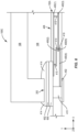
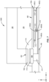
- Figure 4 illustrates a SiP 100A that includes a substrate 102A.
- a metal ring 404 analogous to the metal ring 110, is positioned either on a top surface 406 of the substrate 102A or partially embedded into the substrate 102A.
- At least an upper or top surface 408 of the metal ring 404 is above the top surface 406 of the substrate 102A.
- the metal ring 404 may be considered one of the metal layers of the substrate 102A.
- Vias 410 may interconnect the various metal layers 400(1)-400(N), 402, and 404.
- the various metal layers 400(1)-400(N), 402, and 404 may provide structural rigidity, act as interconnects, ground planes, or the like and no specific restriction is made as to their use.
- a dielectric material 412 is positioned on the top surface 408 of the metal ring 404 and the dielectric contours are substantially congruent thereto. The dielectric material 412 may assist in corrosion prevention for the metal ring 404 as well as help match thermal coefficients.
- the dielectric material 412 may be a solder mask.
- a low modulus epoxy 414 may be used to affix the lid 106 to the metal ring 404.
- the contour of the downwardly-directed lip portion 200 is also substantially congruent to the contours of the metal ring 404.
- any number of metal layers 400(1)-400(N) may be present, however, experimental data suggests that having six or more total metal layers (i.e., N ⁇ 4 or more plus additional metal layer(s) 402 and metal ring 404) provides better resistance to laminate failure and helps decrease the likelihood of gross failure that would allow the air cavity 108 to be compromised.
- Figure 5 illustrates a similar SiP 100B that has one variation relative to the SiP 100A. Specifically, the dielectric material 412 has been replaced with a dielectric layer 500 that covers not just the metal ring 404, but also some portion of the top surface 406 of the substrate 102A. This approach may be easier from a manufacturing perspective as not needing a specific mask to be used during application of the dielectric layer 500.
- Figure 6 illustrates another variation in SiP 100C that has an expanded metal ring 600 and correspondingly larger dielectric material 602.
- the contour of the metal ring 600 it is within the scope of the present disclosure for the contour of the metal ring 600 to be larger than the contour of the lower surface 202 of the lip portion 200 of the lid 106.
- Figure 7 illustrates another variation in SiP 100D that adds an additional dielectric material 700 to the lower surface 202 of the lip portion 200. This may assist in providing better matching of thermal coefficients.
- the thermal coefficients of the dielectric material 412, 500, 602, 700, the epoxy 414, and the lid 106 should be close.
- the modulus of the epoxy 414 will, in part dictate how close the thermal coefficients should be.
- Low modulus epoxies will have low deflections, low bending stresses, and high radii of curvature to generate lower overall vertical (y-axis) deformation.
- the general equations for this are set forth in equations 1 and 2 below.
- Sb is the bending stress and ⁇ is the thermal stress and both are directly proportional to the modulus E of the epoxy 414.
- Sb is also proportional to the temperature change (T) and coefficient of thermal expansion ( ⁇ )
- ⁇ is also proportional to the height (h), inversely proportional to the radius of curvature (R) and Poisson ratio ( ⁇ ).
- lid 106 is generally rectilinear with a single air cavity 108, the present disclosure is not so limited.
- lid 800 in Figure 8 there may be multiple air cavities 802(1)-802(M) formed by interior walls 804.
- lids 900A-900C illustrated in Figures 9A-9C may be non-rectilinear shapes, with lid 900A looking like a capital I, lid 900B having rounded corners 902, and lid 900C looking like an hourglass.
- Other shapes are likewise still within the scope of the present disclosure, with asymmetrical, arcuate, rounded, or other shapes all capable of being used.
- a technique to bond a lid over the air cavity that reduces the risk of cavity integrity failure is provided. More specifically, a metal ring is provided that conforms to or is congruent to a shape of a lower lip of the lid. A dielectric material covers the metal ring, and a low modulus epoxy is used to bind the lower lip of the lid to the dielectric material. The lid and metal ring may have comparable thermal coefficients, which, when coupled with the low modulus epoxy, reduces chance of gross failure of the cavity.
Landscapes
- Structures Or Materials For Encapsulating Or Coating Semiconductor Devices Or Solid State Devices (AREA)
- Packaging Of Annular Or Rod-Shaped Articles, Wearing Apparel, Cassettes, Or The Like (AREA)
Abstract
Description
- The present application claims priority to
U.S. Provisional Patent Application Serial No. 63/363,831, filed on April 29, 2022 - The present application also claims priority to
U.S. Provisional Patent Application Serial No. 63/276,429, filed on November 5, 2021 - The technology of the disclosure relates generally to system in a package (SiP) assemblies that have air cavities.
- Computing devices abound in modern society, and more particularly, mobile communication devices have become increasingly common. The prevalence of these mobile communication devices is driven in part by the many functions that are now enabled on such devices. Increased processing capabilities in such devices means that mobile communication devices have evolved from pure communication tools into sophisticated mobile entertainment centers, thus enabling enhanced user experiences. With the advent of the myriad functions available to such devices, there has been increased pressure to find ways to provide sufficient processing power in a single package. So-called system in a package (SiP) have evolved responsive to this pressure. However, SiP may be vulnerable to package failure and this leaves room for innovation in this space.
- Particular aspects are set out in the appended independent claims. Various optional embodiments are set out in the dependent claims.
- Aspects disclosed in the detailed description include a system in a package (SiP) with an air cavity. In particular, a technique to bond a lid over the air cavity that reduces the risk of cavity integrity failure is provided. More specifically, a metal ring is provided that conforms to or is congruent to a shape of a lower lip of the lid. A dielectric material covers the metal ring, and a low modulus epoxy is used to bind the lower lip of the lid to the dielectric material. The lid and metal ring may have comparable thermal coefficients, which, when coupled with the low modulus epoxy, reduces the chance of gross failure of the cavity.
- In this regard in one aspect, a SiP is disclosed. The SiP comprises a substrate comprising an upper surface. The SiP also comprises a metal ring positioned such that at least a portion extends above the upper surface, the metal ring having a ring contour. The SiP also comprises a lid having a lower lip surface having a lip contour substantially congruent to the ring contour. The SiP also comprises an epoxy attaching the lid to the metal ring.
-
-
Figure 1A is a perspective stylized side elevational view of a system in a package (SiP) according to an example aspect of the present disclosure; -
Figure 1B is a perspective stylized side elevational view of a chiplet in a SiP according to an example aspect of the present disclosure; -
Figure 2 is a perspective cross-sectional elevational view of the SiP ofFigure 1 ; -
Figure 3 is a perspective side elevational view of a SiP with a metal ring to assist in binding a lid to a substrate; -
Figure 4 is a first cross-sectional close-up view of a lid-to-substrate joint; -
Figure 5 is a second cross-sectional close-up view of a lid-to-substrate joint; -
Figure 6 is a third cross-sectional close-up view of a lid-to-substrate joint; -
Figure 7 is a fourth cross-sectional close-up view of a lid-to-substrate joint; -
Figure 8 is a perspective view of a lid with interior compartments; and -
Figures 9A-9C show alternate lid shapes. - The embodiments set forth below represent the necessary information to enable those skilled in the art to practice the embodiments and illustrate the best mode of practicing the embodiments. Upon reading the following description in light of the accompanying drawing figures, those skilled in the art will understand the concepts of the disclosure and will recognize applications of these concepts not particularly addressed herein. It should be understood that these concepts and applications fall within the scope of the disclosure and the accompanying claims.
- It will be understood that, although the terms first, second, etc. may be used herein to describe various elements, these elements should not be limited by these terms. These terms are only used to distinguish one element from another. For example, a first element could be termed a second element, and, similarly, a second element could be termed a first element, without departing from the scope of the present disclosure. As used herein, the term "and/or" includes any and all combinations of one or more of the associated listed items.
- It will be understood that when an element such as a layer, region, or substrate is referred to as being "on" or extending "onto" another element, it can be directly on or extend directly onto the other element or intervening elements may also be present. In contrast, when an element is referred to as being "directly on" or extending "directly onto" another element, there are no intervening elements present. Likewise, it will be understood that when an element such as a layer, region, or substrate is referred to as being "over" or extending "over" another element, it can be directly over or extend directly over the other element or intervening elements may also be present. In contrast, when an element is referred to as being "directly over" or extending "directly over" another element, there are no intervening elements present. It will also be understood that when an element is referred to as being "connected" or "coupled" to another element, it can be directly connected or coupled to the other element or intervening elements may be present. In contrast, when an element is referred to as being "directly connected" or "directly coupled" to another element, there are no intervening elements present.
- Relative terms such as "below" or "above" or "upper" or "lower" or "horizontal" or "vertical" may be used herein to describe a relationship of one element, layer, or region to another element, layer, or region as illustrated in the Figures. It will be understood that these terms and those discussed above are intended to encompass different orientations of the device in addition to the orientation depicted in the Figures.
- The terminology used herein is for the purpose of describing particular embodiments only and is not intended to be limiting of the disclosure. As used herein, the singular forms "a," "an," and "the" are intended to include the plural forms as well, unless the context clearly indicates otherwise. It will be further understood that the terms "comprises," "comprising," "includes," and/or "including" when used herein specify the presence of stated features, integers, steps, operations, elements, and/or components, but do not preclude the presence or addition of one or more other features, integers, steps, operations, elements, components, and/or groups thereof.
- Unless otherwise defined, all terms (including technical and scientific terms) used herein have the same meaning as commonly understood by one of ordinary skill in the art to which this disclosure belongs. It will be further understood that terms used herein should be interpreted as having a meaning that is consistent with their meaning in the context of this specification and the relevant art and will not be interpreted in an idealized or overly formal sense unless expressly so defined herein.
- Aspects disclosed in the detailed description include a system in a package (SiP) with an air cavity. In particular, a technique to bond a lid over the air cavity that reduces the risk of cavity integrity failure is provided. More specifically, a metal ring is provided that conforms to or is congruent to a shape of a lower lip of the lid. A dielectric material covers the metal ring, and a low modulus epoxy is used to bind the lower lip of the lid to the dielectric material. The lid and metal ring may have comparable thermal coefficients, which, when coupled with the low modulus epoxy, reduces the chance of gross failure of the cavity.
- Historically, multiple chips or integrated circuit (IC) dies may be placed on a single substrate and covered with a lid or overmold material, which is typically a plastic material. The lid is bonded to the substrate leaving an air cavity over the chips on the substrate. The lid may have a different thermal coefficient than the substrate and/or the material used to bond the lid to the substrate. The different thermal coefficients may cause the materials to expand and contract at different rates during thermal cycling. Such differences place stress on the bond and may result in failure at the bond. Such failures are undesirable and, when detected during manufacturing, require manual correction, which is slow and adds expense to the component. Accordingly, there is a desire to provide a better bond to prevent such gross package failures.
- Example aspects of the present disclosure provide a technique to provide a better bond between a lid and a substrate that reduces the overall stress on the bond during thermal cycling and reduces the likelihood of gross package failure. In particular, a top surface of a substrate has a metal ring whose contours and area are substantially congruent with the contour of the lower lip of the lid. A dielectric material may coat the metal ring to prevent oxidation and help match thermal coefficients with a low modulus epoxy and the plastic material of the lid. In some aspects, the low modulus epoxy may include a modulus of about 8 megapascals (MPa) or less, to promote flexibility of the bond between the lid and the substrate.
- In this regard,
Figure 1A is side perspective view of aSiP 100 having asubstrate 102 with chips andcomponents 104 mounted thereon. Thesubstrate 102 may be an FR4 material or the like and may include interior metal layers (not shown inFigure 1 but explained in greater detail below). Alid 106 is securely attached or affixed to thesubstrate 102 to create anair cavity 108. More particularly, thelid 106 is affixed to ametal ring 110. - The chips and
components 104 may include various die material(s) such as silicon (Si), gallium arsenide (GaAs), gallium nitride (GaN), silicon germanium (SiGe), indium phosphide (InP), or other material(s). In some aspects, the chips andcomponents 104 may include one or more 'chiplets' 112 as better shown inFigure 1B . Achiplet 112 may comprise asubstrate interposer 114 interconnecting one or more die 116 thereupon. Thesubstrate interposer 114 in some configurations may include semiconducting materials such as Si, silicon carbide (SiC), GaN, and GaAs. Thesubstrate interposer 114 may also comprise a sandwiched network of interconnecting layer(s) deposed between low-k dielectric materials such as Ajinomoto Build-up Film (ABF), glass, or other suitable materials. -
Figure 2 provides a cross-sectional view of theSiP 100 and particularly illustrates the downwardly-directedlip portions 200 of thelid 106. Thelip portions 200 have alower surface 202. Alow modulus epoxy 204 couples thelower surface 202 to themetal ring 110. More details on this coupling are provided with reference toFigures 4-7 below. As noted, in some aspects, the low modulus epoxy may include a modulus of about 8 MPa or less, to promote flexibility of the bond between the lid and the substrate. - The
lid 106 may be formed from a plastic material and thus may be subject to deformation. Accordingly, aninterior wall 206 may be reinforced with an interiormetal wall structure 300 as better seen inFigure 3 . The interiormetal wall structure 300 may be sputtered on theinterior wall 206 and optionally on a top interior surface 208 (better seen inFigure 2 ). Alternatively, the interiormetal wall structure 300 may be formed separately and adhered to theinterior wall 206. The interiormetal wall structure 300 may be conductive (e.g., aluminum (Al), copper (Cu), or silver (Ag) or more expensive metals such as gold (Au) or platinum (Pt)) and thereby also acts to reduce electromagnetic emissions to reduce electromagnetic interference (EMI) and support electromagnetic compatibility (EMC). - There are a variety of ways the
lid 106 may be bonded to thesubstrate 102. Likewise, there are additional details for thesubstrate 102 that may help further support cavity integrity. At a minimum, the contours of the metal ring 110 (sometimes called ring contours) are substantially congruent with the contours of thelower surface 202 of the lip portions 200 (sometimes called lip contours). - As used herein, "congruent" means identical in form; coinciding exactly when superimposed. Further, as used herein, "substantially congruent" means no more than three percent by area of the lower surface is not matched to the metal ring. That is, having a ring that is larger than the lower surface is better than having a lower surface that is larger than the ring, but manufacturing tolerances may create relatively minor variations, and thus, the three percent tolerance where the lower surface may, in such instances, exceed the size of the ring.
- Turning now to
Figures 4-7 , a variety of bonding techniques are illustrated. In particular,Figure 4 illustrates aSiP 100A that includes asubstrate 102A. For the sake of clarity, top, bottom, above, below, upper, and lower as used herein are relative to the y-axis of the Figures and used to help the reader understand relative positions and not absolute requirements. Thesubstrate 102A may have interior metal layers 400(1)-400(N), where, as illustrated, N=4.Additional metal layers 402 may be on a bottom side of thesubstrate 102A. Ametal ring 404, analogous to themetal ring 110, is positioned either on atop surface 406 of thesubstrate 102A or partially embedded into thesubstrate 102A. In either case, at least an upper ortop surface 408 of themetal ring 404 is above thetop surface 406 of thesubstrate 102A. Themetal ring 404 may be considered one of the metal layers of thesubstrate 102A.Vias 410 may interconnect the various metal layers 400(1)-400(N), 402, and 404. The various metal layers 400(1)-400(N), 402, and 404 may provide structural rigidity, act as interconnects, ground planes, or the like and no specific restriction is made as to their use. Adielectric material 412 is positioned on thetop surface 408 of themetal ring 404 and the dielectric contours are substantially congruent thereto. Thedielectric material 412 may assist in corrosion prevention for themetal ring 404 as well as help match thermal coefficients. In an example aspect, thedielectric material 412 may be a solder mask. Alow modulus epoxy 414 may be used to affix thelid 106 to themetal ring 404. As described above, the contour of the downwardly-directedlip portion 200 is also substantially congruent to the contours of themetal ring 404. - In general, any number of metal layers 400(1)-400(N) may be present, however, experimental data suggests that having six or more total metal layers (i.e., N ≥ 4 or more plus additional metal layer(s) 402 and metal ring 404) provides better resistance to laminate failure and helps decrease the likelihood of gross failure that would allow the
air cavity 108 to be compromised. -
Figure 5 illustrates asimilar SiP 100B that has one variation relative to theSiP 100A. Specifically, thedielectric material 412 has been replaced with adielectric layer 500 that covers not just themetal ring 404, but also some portion of thetop surface 406 of thesubstrate 102A. This approach may be easier from a manufacturing perspective as not needing a specific mask to be used during application of thedielectric layer 500. -
Figure 6 illustrates another variation inSiP 100C that has an expandedmetal ring 600 and correspondingly largerdielectric material 602. Thus, as noted above, it is within the scope of the present disclosure for the contour of themetal ring 600 to be larger than the contour of thelower surface 202 of thelip portion 200 of thelid 106. -
Figure 7 illustrates another variation inSiP 100D that adds an additionaldielectric material 700 to thelower surface 202 of thelip portion 200. This may assist in providing better matching of thermal coefficients. - In general, to assist in prevention of delamination or failure of the bond between the
lid 106 and thesubstrate dielectric material lid 106 should be close. The modulus of the epoxy 414 will, in part dictate how close the thermal coefficients should be. Low modulus epoxies will have low deflections, low bending stresses, and high radii of curvature to generate lower overall vertical (y-axis) deformation. The general equations for this are set forth inequations 

- Where Sb is the bending stress and σ is the thermal stress and both are directly proportional to the modulus E of the
epoxy 414. Sb is also proportional to the temperature change (T) and coefficient of thermal expansion (α), σ is also proportional to the height (h), inversely proportional to the radius of curvature (R) and Poisson ratio (γ). - Note that while the above discussion has shown the
lid 106 as being generally rectilinear with asingle air cavity 108, the present disclosure is not so limited. Thus, as illustrated bylid 800 inFigure 8 , there may be multiple air cavities 802(1)-802(M) formed byinterior walls 804. - Likewise,
lids 900A-900C, illustrated inFigures 9A-9C may be non-rectilinear shapes, withlid 900A looking like a capital I,lid 900B having roundedcorners 902, andlid 900C looking like an hourglass. Other shapes are likewise still within the scope of the present disclosure, with asymmetrical, arcuate, rounded, or other shapes all capable of being used. - Therefore, from one perspective, there has been described a system in package (SiP) with an air cavity. In one aspect, a technique to bond a lid over the air cavity that reduces the risk of cavity integrity failure is provided. More specifically, a metal ring is provided that conforms to or is congruent to a shape of a lower lip of the lid. A dielectric material covers the metal ring, and a low modulus epoxy is used to bind the lower lip of the lid to the dielectric material. The lid and metal ring may have comparable thermal coefficients, which, when coupled with the low modulus epoxy, reduces chance of gross failure of the cavity.
- Further examples are set out in the following numbered clauses:
-
Clause 1. A system in a package (SiP) comprising: a substrate comprising an upper surface; a metal ring positioned such that at least a portion extends above the upper surface, the metal ring having a ring contour; a lid having a lower lip surface having a lip contour substantially congruent to the ring contour; and an epoxy attaching the lid to the metal ring. -
Clause 2. The SiP ofclause 1, further comprising a dielectric material positioned on the metal ring. -
Clause 3. The SiP ofclause 2, wherein the dielectric material has a dielectric contour substantially congruent to the ring contour. -
Clause 4. The SiP ofclause - Clause 5. The SiP of
clause - Clause 6. The SiP of any preceding clause, wherein the epoxy comprises a low modulus epoxy.
- Clause 7. The SiP of any preceding clause, wherein the lid and the epoxy have approximately equal thermal coefficients.
- Clause 8. The SiP of any preceding clause, wherein the lid delimits an air cavity above the substrate.
- Clause 9. The SiP of any preceding clause further comprising an interior metal wall positioned within the lid.
- Clause 10. The SiP of any preceding clause, further comprising an interior metal layer sputtered on an interior surface of the lid.
-
Clause 11. The SiP of any preceding clause, further comprising one or more chips positioned on the substrate. - Clause 12. The SiP of any preceding clause, wherein the substrate comprises a plurality of interior metal layers.
- Clause 13. The SiP of clause 12, wherein the plurality of interior metal layers comprises more than three interior metal layers.
-
Clause 14. The SiP of any preceding clause, further comprising a plurality of chiplets positioned on the substrate. - Clause 15. The SiP of
clause 14, wherein each of the plurality of chiplets comprises a substrate interposer, wherein the substrate interposer comprises one or one or more low-k dielectric layers interposed by one or more metal layers, the metal layers interconnecting one or more die within a chiplet. - Clause 16. The SiP of
clause 14, wherein each of the plurality of chiplets comprises a substrate interposer, wherein the substrate interposer comprises one or one or more low-k dielectric layers interposed by one or more metal layers disposed upon a semiconducting material, the metal layers interconnecting one or more die within a chiplet. - Clause 17. The SiP of any preceding clause, wherein the lid comprises a plastic material.
- Clause 18. The SiP of any preceding clause, wherein an area within the ring contour has a greater area than an area inside the lip contour.
- It is also noted that the operational steps described in any of the example aspects herein are described to provide examples and discussion. The operations described may be performed in numerous different sequences other than the illustrated sequences. Furthermore, operations described in a single operational step may actually be performed in a number of different steps. Additionally, one or more operational steps discussed in the example aspects may be combined. It is to be understood that the operational steps illustrated in the flowchart diagrams may be subject to numerous different modifications as will be readily apparent to one of skill in the art. Those of skill in the art will also understand that information and signals may be represented using any of a variety of different technologies and techniques. For example, data, instructions, commands, information, signals, bits, symbols, and chips that may be referenced throughout the above description may be represented by voltages, currents, electromagnetic waves, magnetic fields or particles, optical fields or particles, or any combination thereof.
- The previous description of the disclosure is provided to enable any person skilled in the art to make or use the disclosure. Various modifications to the disclosure will be readily apparent to those skilled in the art, and the generic principles defined herein may be applied to other variations. Thus, the disclosure is not intended to be limited to the examples and designs described herein but is to be accorded the widest scope consistent with the principles and novel features disclosed herein.
Claims (15)
- A system in a package (SiP) comprising:a substrate comprising an upper surface;a metal ring positioned such that at least a portion extends above the upper surface, the metal ring having a ring contour;a lid having a lower lip surface having a lip contour substantially congruent to the ring contour; andan epoxy attaching the lid to the metal ring.
- The SiP of claim 1, further comprising a dielectric material positioned on the metal ring.
- The SiP of claim 2, wherein the dielectric material has a dielectric contour substantially congruent to the ring contour and/or wherein the dielectric material covers an upper surface of the metal ring and at least part of the upper surface of the substrate.
- The SiP of claim 2 or 3, further comprising a second dielectric material positioned on a lower surface of the lower lip surface.
- The SiP of any preceding claim, wherein the epoxy comprises a low modulus epoxy.
- The SiP of any preceding claim, wherein the lid and the epoxy have approximately equal thermal coefficients.
- The SiP of any preceding claim, wherein the lid delimits an air cavity above the substrate.
- The SiP of any preceding claim further comprising an interior metal wall positioned within the lid.
- The SiP of any preceding claim, further comprising an interior metal layer sputtered on an interior surface of the lid.
- The SiP of any preceding claim, further comprising one or more chips positioned on the substrate.
- The SiP of any preceding claim, wherein the substrate comprises a plurality of interior metal layers, for example wherein the plurality of interior metal layers comprises more than three interior metal layers.
- The SiP of any preceding claim, further comprising a plurality of chiplets positioned on the substrate.
- The SiP of claim 12, wherein each of the plurality of chiplets comprises one or more selected from the group comprising: a substrate interposer, wherein the substrate interposer comprises one or one or more low-k dielectric layers interposed by one or more metal layers, the metal layers interconnecting one or more die within a chiplet; and a substrate interposer, wherein the substrate interposer comprises one or one or more low-k dielectric layers interposed by one or more metal layers disposed upon a semiconducting material, the metal layers interconnecting one or more die within a chiplet.
- The SiP of any preceding claim, wherein the lid comprises a plastic material.
- The SiP of any preceding claim, wherein an area within the ring contour has a greater area than an area inside the lip contour.
Applications Claiming Priority (3)
| Application Number | Priority Date | Filing Date | Title |
|---|---|---|---|
| US202163276429P | 2021-11-05 | 2021-11-05 | |
| US202263363831P | 2022-04-29 | 2022-04-29 | |
| US17/819,203 US12512375B2 (en) | 2021-11-05 | 2022-08-11 | System in a package (SIP) with air cavity |
Publications (2)
| Publication Number | Publication Date |
|---|---|
| EP4177939A2 true EP4177939A2 (en) | 2023-05-10 |
| EP4177939A3 EP4177939A3 (en) | 2023-08-02 |
Family
ID=84361283
Family Applications (1)
| Application Number | Title | Priority Date | Filing Date |
|---|---|---|---|
| EP22205106.2A Pending EP4177939A3 (en) | 2021-11-05 | 2022-11-02 | System in a package (sip) with air cavity |
Country Status (3)
| Country | Link |
|---|---|
| US (1) | US12512375B2 (en) |
| EP (1) | EP4177939A3 (en) |
| CN (1) | CN116093027A (en) |
Family Cites Families (10)
| Publication number | Priority date | Publication date | Assignee | Title |
|---|---|---|---|---|
| US6909176B1 (en) * | 2003-11-20 | 2005-06-21 | Altera Corporation | Structure and material for assembling a low-K Si die to achieve a low warpage and industrial grade reliability flip chip package with organic substrate |
| JP5277755B2 (en) * | 2008-07-01 | 2013-08-28 | オムロン株式会社 | Electronic components |
| US8723308B2 (en) | 2010-11-19 | 2014-05-13 | Analog Devices, Inc. | Packages and methods for packaging using a lid having multiple conductive layers |
| US9721903B2 (en) * | 2015-12-21 | 2017-08-01 | Apple Inc. | Vertical interconnects for self shielded system in package (SiP) modules |
| WO2017142978A1 (en) * | 2016-02-15 | 2017-08-24 | Transsip Inc | Emi shielded integrated circuit packages and methods of making the same |
| US10141271B1 (en) | 2017-03-17 | 2018-11-27 | CoolStar Technology, Inc. | Semiconductor device having enhanced high-frequency capability and methods for making same |
| US10943869B2 (en) * | 2017-06-09 | 2021-03-09 | Apple Inc. | High density interconnection using fanout interposer chiplet |
| US11380624B2 (en) | 2017-09-30 | 2022-07-05 | Intel Corporation | Electromagnetic interference shield created on package using high throughput additive manufacturing |
| US11219144B2 (en) * | 2018-06-28 | 2022-01-04 | Qorvo Us, Inc. | Electromagnetic shields for sub-modules |
| US11749631B2 (en) * | 2020-05-20 | 2023-09-05 | Apple Inc. | Electronic package including a hybrid thermal interface material and low temperature solder patterns to improve package warpage and reliability |
-
2022
- 2022-08-11 US US17/819,203 patent/US12512375B2/en active Active
- 2022-11-02 EP EP22205106.2A patent/EP4177939A3/en active Pending
- 2022-11-04 CN CN202211374359.6A patent/CN116093027A/en active Pending
Also Published As
| Publication number | Publication date |
|---|---|
| EP4177939A3 (en) | 2023-08-02 |
| US20230145639A1 (en) | 2023-05-11 |
| CN116093027A (en) | 2023-05-09 |
| US12512375B2 (en) | 2025-12-30 |
Similar Documents
| Publication | Publication Date | Title |
|---|---|---|
| US12381119B2 (en) | Seal for microelectronic assembly | |
| US6134776A (en) | Heatsink and package structure for wirebond chip rework and replacement | |
| US5900675A (en) | Organic controlled collapse chip connector (C4) ball grid array (BGA) chip carrier with dual thermal expansion rates | |
| US7417310B2 (en) | Circuit module having force resistant construction | |
| JP2001506057A (en) | Chip-scale ball grid array for integrated circuit packages | |
| CN1462071A (en) | System for flexible interconnection packaging | |
| WO1999018609A1 (en) | Chip scale ball grid array for integrated circuit package | |
| EP0928022A2 (en) | Resin package fabrication process | |
| US11664302B2 (en) | Integrated circuit module with a structurally balanced package using a bottom side interposer | |
| US10916507B2 (en) | Multiple chip carrier for bridge assembly | |
| EP2006248B1 (en) | Die mounting stress isolator | |
| US11676900B2 (en) | Electronic assembly that includes a bridge | |
| US7253504B1 (en) | Integrated circuit package and method | |
| US20210403318A1 (en) | Semiconductor Package With Built-In Vibration Isolation, Thermal Stability, And Connector Decoupling | |
| US12512375B2 (en) | System in a package (SIP) with air cavity | |
| US6351389B1 (en) | Device and method for packaging an electronic device | |
| US20040226688A1 (en) | Application specific apparatus for dissipating heat from multiple electronic components | |
| US5825093A (en) | Attachment system and method therefor | |
| US11121048B1 (en) | System and method for a device package | |
| US8975738B2 (en) | Structure for microelectronic packaging with terminals on dielectric mass | |
| US20230402333A1 (en) | System in a package (sip) with air cavity and epoxy seal | |
| US20040218363A1 (en) | Application specific heat-dissipating apparatus that provides electrical isolation for components | |
| JPH0331086Y2 (en) | ||
| US20060006508A1 (en) | Semiconductor device in which semiconductor chip is mounted on lead frame | |
| WO1998048449A2 (en) | Flip chip and chip scale package |
Legal Events
| Date | Code | Title | Description |
|---|---|---|---|
| PUAI | Public reference made under article 153(3) epc to a published international application that has entered the european phase |
Free format text: ORIGINAL CODE: 0009012 |
|
| STAA | Information on the status of an ep patent application or granted ep patent |
Free format text: STATUS: THE APPLICATION HAS BEEN PUBLISHED |
|
| AK | Designated contracting states |
Kind code of ref document: A2 Designated state(s): AL AT BE BG CH CY CZ DE DK EE ES FI FR GB GR HR HU IE IS IT LI LT LU LV MC ME MK MT NL NO PL PT RO RS SE SI SK SM TR |
|
| PUAL | Search report despatched |
Free format text: ORIGINAL CODE: 0009013 |
|
| AK | Designated contracting states |
Kind code of ref document: A3 Designated state(s): AL AT BE BG CH CY CZ DE DK EE ES FI FR GB GR HR HU IE IS IT LI LT LU LV MC ME MK MT NL NO PL PT RO RS SE SI SK SM TR |
|
| RIC1 | Information provided on ipc code assigned before grant |
Ipc: H01L 25/18 20230101ALN20230623BHEP Ipc: H01L 25/16 20230101ALN20230623BHEP Ipc: H01L 25/065 20230101ALN20230623BHEP Ipc: H01L 23/538 20060101ALN20230623BHEP Ipc: H01L 23/498 20060101ALN20230623BHEP Ipc: H01L 23/00 20060101ALN20230623BHEP Ipc: H01L 23/58 20060101ALI20230623BHEP Ipc: H01L 23/053 20060101ALI20230623BHEP Ipc: H01L 23/10 20060101AFI20230623BHEP |
|
| STAA | Information on the status of an ep patent application or granted ep patent |
Free format text: STATUS: REQUEST FOR EXAMINATION WAS MADE |
|
| 17P | Request for examination filed |
Effective date: 20240129 |
|
| RBV | Designated contracting states (corrected) |
Designated state(s): AL AT BE BG CH CY CZ DE DK EE ES FI FR GB GR HR HU IE IS IT LI LT LU LV MC ME MK MT NL NO PL PT RO RS SE SI SK SM TR |