EP4176470B1 - Verbesserte lichtemittierende vorrichtungen - Google Patents
Verbesserte lichtemittierende vorrichtungen Download PDFInfo
- Publication number
- EP4176470B1 EP4176470B1 EP21740184.3A EP21740184A EP4176470B1 EP 4176470 B1 EP4176470 B1 EP 4176470B1 EP 21740184 A EP21740184 A EP 21740184A EP 4176470 B1 EP4176470 B1 EP 4176470B1
- Authority
- EP
- European Patent Office
- Prior art keywords
- emissive
- light emitting
- blue
- emissive unit
- blue light
- Prior art date
- Legal status (The legal status is an assumption and is not a legal conclusion. Google has not performed a legal analysis and makes no representation as to the accuracy of the status listed.)
- Active
Links
Images


Classifications
-
- H—ELECTRICITY
- H10—SEMICONDUCTOR DEVICES; ELECTRIC SOLID-STATE DEVICES NOT OTHERWISE PROVIDED FOR
- H10K—ORGANIC ELECTRIC SOLID-STATE DEVICES
- H10K50/00—Organic light-emitting devices
- H10K50/10—OLEDs or polymer light-emitting diodes [PLED]
- H10K50/11—OLEDs or polymer light-emitting diodes [PLED] characterised by the electroluminescent [EL] layers
- H10K50/125—OLEDs or polymer light-emitting diodes [PLED] characterised by the electroluminescent [EL] layers specially adapted for multicolour light emission, e.g. for emitting white light
- H10K50/13—OLEDs or polymer light-emitting diodes [PLED] characterised by the electroluminescent [EL] layers specially adapted for multicolour light emission, e.g. for emitting white light comprising stacked EL layers within one EL unit
- H10K50/131—OLEDs or polymer light-emitting diodes [PLED] characterised by the electroluminescent [EL] layers specially adapted for multicolour light emission, e.g. for emitting white light comprising stacked EL layers within one EL unit with spacer layers between the electroluminescent layers
-
- H—ELECTRICITY
- H10—SEMICONDUCTOR DEVICES; ELECTRIC SOLID-STATE DEVICES NOT OTHERWISE PROVIDED FOR
- H10K—ORGANIC ELECTRIC SOLID-STATE DEVICES
- H10K59/00—Integrated devices, or assemblies of multiple devices, comprising at least one organic light-emitting element covered by group H10K50/00
- H10K59/30—Devices specially adapted for multicolour light emission
- H10K59/32—Stacked devices having two or more layers, each emitting at different wavelengths
-
- H—ELECTRICITY
- H10—SEMICONDUCTOR DEVICES; ELECTRIC SOLID-STATE DEVICES NOT OTHERWISE PROVIDED FOR
- H10K—ORGANIC ELECTRIC SOLID-STATE DEVICES
- H10K59/00—Integrated devices, or assemblies of multiple devices, comprising at least one organic light-emitting element covered by group H10K50/00
- H10K59/30—Devices specially adapted for multicolour light emission
- H10K59/35—Devices specially adapted for multicolour light emission comprising red-green-blue [RGB] subpixels
-
- H—ELECTRICITY
- H10—SEMICONDUCTOR DEVICES; ELECTRIC SOLID-STATE DEVICES NOT OTHERWISE PROVIDED FOR
- H10K—ORGANIC ELECTRIC SOLID-STATE DEVICES
- H10K50/00—Organic light-emitting devices
- H10K50/10—OLEDs or polymer light-emitting diodes [PLED]
- H10K50/19—Tandem OLEDs
-
- H—ELECTRICITY
- H10—SEMICONDUCTOR DEVICES; ELECTRIC SOLID-STATE DEVICES NOT OTHERWISE PROVIDED FOR
- H10K—ORGANIC ELECTRIC SOLID-STATE DEVICES
- H10K50/00—Organic light-emitting devices
- H10K50/80—Constructional details
- H10K50/805—Electrodes
- H10K50/81—Anodes
-
- H—ELECTRICITY
- H10—SEMICONDUCTOR DEVICES; ELECTRIC SOLID-STATE DEVICES NOT OTHERWISE PROVIDED FOR
- H10K—ORGANIC ELECTRIC SOLID-STATE DEVICES
- H10K50/00—Organic light-emitting devices
- H10K50/80—Constructional details
- H10K50/805—Electrodes
- H10K50/82—Cathodes
-
- H—ELECTRICITY
- H10—SEMICONDUCTOR DEVICES; ELECTRIC SOLID-STATE DEVICES NOT OTHERWISE PROVIDED FOR
- H10K—ORGANIC ELECTRIC SOLID-STATE DEVICES
- H10K59/00—Integrated devices, or assemblies of multiple devices, comprising at least one organic light-emitting element covered by group H10K50/00
- H10K59/30—Devices specially adapted for multicolour light emission
- H10K59/38—Devices specially adapted for multicolour light emission comprising colour filters or colour changing media [CCM]
-
- H—ELECTRICITY
- H10—SEMICONDUCTOR DEVICES; ELECTRIC SOLID-STATE DEVICES NOT OTHERWISE PROVIDED FOR
- H10K—ORGANIC ELECTRIC SOLID-STATE DEVICES
- H10K85/00—Organic materials used in the body or electrodes of devices covered by this subclass
- H10K85/50—Organic perovskites; Hybrid organic-inorganic perovskites [HOIP], e.g. CH3NH3PbI3
-
- H—ELECTRICITY
- H10—SEMICONDUCTOR DEVICES; ELECTRIC SOLID-STATE DEVICES NOT OTHERWISE PROVIDED FOR
- H10K—ORGANIC ELECTRIC SOLID-STATE DEVICES
- H10K50/00—Organic light-emitting devices
- H10K50/10—OLEDs or polymer light-emitting diodes [PLED]
- H10K50/11—OLEDs or polymer light-emitting diodes [PLED] characterised by the electroluminescent [EL] layers
- H10K50/115—OLEDs or polymer light-emitting diodes [PLED] characterised by the electroluminescent [EL] layers comprising active inorganic nanostructures, e.g. luminescent quantum dots
Definitions
- the present invention relates to novel light emitting device architectures for application in displays, light panels and other optoelectronic devices, and in particular to stacked blue light emitting devices that comprise two or more emissive units that emit blue light having substantially different chromaticity.
- OLED Organic Light Emitting Diode
- LCD liquid crystal display
- OLED smartphones comprise an RGB OLED display architecture where red, green and blue organic light emitting materials are patterned into separate red, green and blue sub-pixels that emit red, green and blue light.
- An exemplary RGB OLED display architecture is depicted by arrangement 1800 in FIG. 18 .
- the device of the red sub-pixel 1805 comprises a red emissive layer 1840.
- the device of the green sub-pixel 1815 comprises a green emissive layer 1850.
- the device of the blue sub-pixel 1825 comprises a blue emissive layer 1860.
- the red, green and blue emissive layers are disposed between a first electrode 1820 and a second electrode 1830. All layers are disposed on a substrate 1810.
- the exemplary RGB OLED display architecture of arrangement 1800 may include optional additional device layers that are not depicted in FIG. 18 .
- Patterning of red, green and blue emissive layers is achieved by depositing red, green and blue organic light emitting materials by vapour thermal evaporation through fine metal masks with openings that are precisely aligned to the respective red, green and blue sub-pixels.
- the RGB OLED display architecture delivers high performance because each of the red, green and blue sub-pixels may be individually optimized to emit efficient, bright and vibrant light.
- the RGB OLED display architecture is also relatively low cost because each of the red, green and blue sub-pixels typically comprises a simple OLED device stack of approximately 6-7 evaporated layers.
- the RGB OLED display architecture used so successfully in smartphones has not been successfully scaled for application in televisions.
- the problem is that manufacturing televisions requires larger glass substrates (e.g. 3130 mm x 2880 mm Gen 10 substrates) than manufacturing smartphones (e.g. 1800 mm x 1500 mm Gen 6 substrates).
- the fine metal masks required to pattern red, green and blue organic light emitting material into red, green and blue sub-pixels then have the tendency to sag over the larger substrate area leading to misalignment and undesirable shadowing effects.
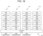
- OLED televisions instead comprise an RGBW OLED display architecture where each sub-pixel of the display comprises a white OLED. Individual patterning of different sub-pixels is not required.
- An exemplary RGBW OLED display architecture is depicted by arrangement 1900 in FIG. 19 . Colour filters of red, green and blue are patterned over three-out-of-four of the white OLED sub-pixels.
- the device of the red sub-pixel 1905 comprises a white OLED optically coupled to a red colour filter 1985.
- the device of the green sub-pixel 1915 comprises a white OLED optically coupled to a green colour filter 1990.
- the device of the blue sub-pixel 1925 comprises a white OLED optically coupled to a blue colour filter 1995.
- the device of the white sub-pixel 1935 comprises a white OLED without a colour filter.
- Each white OLED comprises a stacked light emitting device having three emissive units comprising a red emissive layer 1930, a green emissive layer 1950 and a blue emissive layer 1970 all disposed between a first electrode 1920 and a second electrode 1980.
- the red emissive layer 1930 is separated from the green emissive layer 1950 by a first charge generation layer 1940.
- the green emissive layer 1950 is separated from the blue emissive layer 1970 by a second charge generation layer 1960. All layers are disposed on a substrate 1910.
- the exemplary RGBW OLED display architecture of arrangement 1900 may include optional additional device layers that are not depicted in FIG. 19 .
- the RGBW OLED display architecture used in OLED televisions delivers reduced performance compared to the RGB OLED display architecture used in OLED smartphones. The is because the majority of light emitted from the white OLEDs in the red, green and blue sub-pixels is filtered out. This reduces the efficiency and brightness of the display.
- the colorfulness of an RGBW OLED display is also limited because there is a trade-off between using stronger colour filters to extend the colour gamut of the display and reducing brightness by filtering out more white light.
- the RGBW OLED display architecture is also relatively expensive because each of the red, green and blue sub-pixels typically comprises a white OLED device stack of approximately 15-20 evaporated layers.
- OLED televisions with an RGBW OLED display architecture are therefore less efficient, less bright, less stylish and relatively more expensive than OLED smartphones with an RGB OLED display architecture. This is why OLED technology is widely adopted in smartphones but not in televisions.
- a novel QD-OLED display architecture was recently proposed by Samsung.
- An exemplary QD-OLED display architecture is depicted by arrangement 2000 in FIG. 20 .
- each sub-pixel of the display comprises a blue OLED. Colour conversion layers of red and green are then patterned over two-out-of-three of the blue OLED sub-pixels.
- the device of the red sub-pixel 2005 comprises a blue emissive layer 2040 optically coupled to a red colour conversion layer 2050.
- the device of the green sub-pixel 2015 comprises a blue emissive layer 2040 optically coupled to a green colour conversion layer 2060.
- the device of the blue sub-pixel 2025 comprises a blue emissive layer 2040 without a colour conversion layer.
- the blue emissive layers are disposed between a first electrode 2020 and a second electrode 2030. All layers are disposed on a substrate 2010.
- the exemplary QD-OLED display architecture of arrangement 2000 may include optional additional device layers that are not depicted in FIG. 20 .
- the red and green colour conversion layers comprise quantum dot (QD) material which gives rise to the name of QD-OLED for this display architecture.
- QD quantum dot
- the QD-OLED display architecture is expected to be an improvement over the RGBW OLED display architecture. This is because converting blue light to red light or green light using colour conversion layers is a more efficient process than filtering white light to red, green or blue light using colour filters. QD-OLED displays are therefore expected to be more efficient, brighter and more stylish than RGBW OLED displays. Furthermore, the blue OLED device stack in a QD-OLED display may be simpler and may comprise fewer layers than the white OLED stack in an RGBW OLED display. This reduces costs. These improvements may all be achieved without fine metal mask technology because as for RGBW OLED displays, QD-OLED displays may be manufactured without individual patterning of light-emitting materials for the different sub-pixels.
- the proposed QD-OLED display architecture does suffer from drawbacks.
- one significant drawback is that the lifetime of blue OLED devices is typically shorter than for red and green OLED devices, and in the QD-OLED display architecture blue OLEDs are used to provide light for the red and green sub-pixels as well as for the blue sub-pixels. This is expected to limit the lifetime of a QD-OLED display.
- blue light emitted by the blue OLEDs must be highly saturated to enable the display to render deep blue colours and an extended colour gamut.
- the problem is that deep blue phosphorescent emitters that have higher efficiency are relatively unstable and unsuitable for commercial applications. It is therefore expected that deep blue fluorescent emitters that have lower efficiency, but relatively improved stability will be required.
- blue light emitted by the blue OLEDs must be simultaneously optimized to match the absorption of the red and green colour conversion materials and to be deep enough to enable a display to render deep blue colours for an extended colour gamut. There is likely a trade-off that will result in reduced performance.
- the present invention addresses these problems by proposing a stacked blue light emitting device architecture comprising two or more emissive units that emit blue light having substantially different chromaticity for application in displays, light panels and other optoelectronic devices.
- at least one emissive unit may emit deeper blue light and at least one emissive unit may emit lighter blue light.
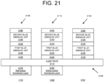
- the proposed architecture is depicted by exemplary arrangement 2100 in FIG. 21 for a stacked blue light emitting device having two emissive units.
- the device of the red sub-pixel 2105 comprises a first blue emissive unit 2130 and a second blue emissive unit 2150 separated by a first charge generation layer 2140 and optically coupled to a red colour conversion layer 2170.
- the device of the green sub-pixel 2115 comprises a first blue emissive unit 2130 and a second blue emissive unit 2150 separated by a first charge generation layer 2140 and optically coupled to a green colour conversion layer 2180.
- the device of the blue sub-pixel 2125 comprises a first blue emissive unit 2130 and a second blue emissive unit 2150 separated by a first charge generation layer 2140.
- the layers of the first and second blue emissive units and first charge generation layer are all disposed between a first electrode 2120 and a second electrode 2160. All layers are disposed on a substrate 2110. At least one of the first blue emissive unit 2130 and the second blue emissive unit 2150 may emit a lighter blue light, and at least one of the first blue emissive unit 2130 and the second blue emissive unit 2150 may emit a deeper blue light.
- the stacked blue light emitting device architecture of the present invention may comprise a third emissive unit 2220 and a second charge generation layer 2210. This is depicted by exemplary arrangement 2200 in FIG. 22 for a stacked blue light emitting device having three emissive units.
- the third emissive unit 2220 may emit a lighter blue light or a deeper blue light.
- the emissive units may be addressed independently and may emit light independently of each other.
- the emissive units may be commonly addressed and may not emit light independently of each other.
- Such stacked blue light emitting devices may be incorporated into the red, green and blue sub-pixels of an OLED display.
- the blue sub-pixel of such a display is required to emit a relatively saturated blue light that is more saturated than light that may be emitted from the lighter blue emissive units, but less saturated than light that may be emitted from the deeper blue emissive units
- the emissive unit that emits deeper blue light may be individually addressed and may emit light to generate the display image while the emissive unit that emits lighter blue light may remain inactive.
- the emissive unit that emits lighter blue light may be individually addressed and may emit light to generate the display image while the emissive unit that emits deeper blue light may remain inactive.
- Light may be emitted from the relatively more efficient and/or stable lighter blue emissive unit to render the majority of display images, with light emitted from the relatively less efficient and/or stable deeper blue emissive unit only required to render a small proportion of images. The efficiency and/or lifetime of the display may therefore be enhanced.
- the lighter blue emissive unit may be used on its own or in combination with the deeper blue emissive unit to provide light to the red and green colour conversion layers in the red and green sub-pixels.
- the lighter blue emissive unit may comprise a phosphorescent organic light emitting material or a fluorescent organic light emitting material.
- the deeper blue emissive unit may comprise a phosphorescent organic light emitting material or a fluorescent organic light emitting material.
- the lighter blue emissive unit may comprise a fluorescent organic light emitting material and the deeper blue emissive unit may comprise a fluorescent organic light emitting material.
- the lighter blue emissive unit may comprise a phosphorescent organic light emitting material and the deeper blue emissive unit may comprise a phosphorescent organic light emitting material.
- the lighter blue emissive unit may comprise a phosphorescent organic light emitting material and the deeper blue emissive unit may comprise a fluorescent organic light emitting material.
- the proposed novel device architecture is ideally suited to OLED devices and displays.
- the proposed novel device architecture is also ideally suited to quantum dot light emitting diode (QLED) displays comprising quantum dot light emitting material and perovskite light emitting diode (PeLED) displays comprising perovskite light emitting material.
- QLED quantum dot light emitting diode
- PeLED perovskite light emitting diode
- Inherent properties of organic light emitting materials, quantum dot light emitting materials and perovskite light emitting materials render them well-suited to the herein disclosed stacked blue light emitting device architecture. These properties include optical band gaps that are readily tunable across the visible, ultra-violet and infra-red spectra, high colour saturation that enables displays with wide colour gamut, excellent charge transport properties and low non-radiative rates.
- WO 2019/224546 A1 discloses a stacked light emitting device comprising at least one PeLED emissive unit and at least one PeLED, OLED or QLED emissive unit.
- the emissive units may be of any colour and may be commonly or independently addressable.
- the emissive units may be optically coupled to one or more colour conversion layers. This has the benefit of enabling different classes of emissive materials, such as OLED, QLED and PeLED to be combined in a stacked light emitting device.
- WO 2019/224546 A1 does not disclose details of how such a stacked light emitting device architecture may be implemented in one or more sub-pixels of a display. Furthermore, it does not disclose any embodiments where the emissive units may be of different chromaticity or describe any applications or advantages of having emissive units of different chromaticity. It only discloses chromaticity data for exemplary emissive units comprising different classes of emissive materials. Unlike the present disclosure, WO 2019/224546 A1 is also limited to stacked light emitting devices where one or more PeLED emissive units and combined with one or more PeLED, OLED or QLED emissive units. It does not include stacked light emitting devices comprising only OLED, only QLED or only PeLED emissive units, which would be simpler to manufacture.
- US 2019/0043407 A1 discloses a pixel layout for a display comprising a blue sub-pixel that comprises a stacked blue light emitting device having two blue emissive units of different chromaticities that are independently addressable, and (as disclosed in paragraph [0043] and [0057]) red and green sub-pixels that are single junction (not stacked) light emitting devices.
- the pixel layout disclosed in US 2019/0043407 A1 does not comprise red and green colour conversion layers, and requires that red, green and blue emissive units be individually patterned into their respective sub-pixels. This may add complexity and cost to the manufacturing process and may be difficult to scale to larger area substrates.
- EP 3188272 A1 discloses a stacked blue light emitting device comprising a first emissive unit and a second emissive unit separated by a charge generation layer.
- the first emissive unit comprises a first emissive layer that emits blue light
- the second emissive unit comprises a second emissive layer that emits blue light, wherein the first and second emissive layers emit light of different chromaticity.
- a display architecture wherein there are colour conversion materials over the red and green sub-pixels. Unlike the present disclosure, the emissive units disclosed in EP 3188272 A1 in FIG. 7 and FIG.
- WO 2020/030042 A1 discloses an OLED display comprising at least a first blue emissive layer and one or more additional blue emissive layers disposed over the entire display area of a substrate, and a quantum dot colour film disposed on the light-emitting side of the substrate.
- Paragraphs [0065] and [0066] describe that the blue emissive layers emit blue light of different chromaticity, with one emitting at 400-440 nm, and the other emitting at 440-490 nm.
- the quantum dot film may comprise red quantum dots for the red sub-pixel and green quantum dots for the green sub-pixel.
- the blue sub-pixel may or may not comprise quantum dots.
- the blue emissive layers may be connected in series by a charge generation layer as in a standard stacked device, or there may be separate anode and cathodes for each emissive unit that are electrically connected in series.
- the emissive layers disclosed in WO 2020/030042 A1 are described as being connected in series.
- OLED materials and configurations are described in Uoyama et al. and in European patent EP 0423283 B1 and United States patents US 6303238 B1 and US 7279704 B2 .
- QLED materials and configurations are described in Kathirgamanathan et al.
- PeLED materials and configurations are described in Adjokatse et al.
- organic includes polymeric materials as well as small molecule organic materials that may be used to fabricate optoelectronic devices, such as OLEDs.
- small molecule refers to any organic material that is not a polymer, and small molecules may actually be quite large. Small molecules may include repeat units in some circumstances. For example, using a long chain alkyl group as a substituent does not remove a molecule from the small molecule class. Small molecules may also be incorporated into polymers, for example as a pendant group on a polymer backbone or as part of the backbone.
- a dendrimer may be a small molecule and it is believed that all dendrimers currently used in the field of OLEDs are small molecules.
- organic light emitting material includes fluorescent and phosphorescent organic light emitting materials, as well as organic materials that emit light through mechanisms such as triplet-triplet annihilation (TTA) or thermally activated delayed fluorescence (TADF) or hyperfluorescence.
- organic materials that emit light through mechanisms such as TADF or hyperfluorescence are considered fluorescent organic light emitting materials.
- organic light emitting material that emits red light is bis(2-(3,5-dimethylphenyl)quinoline-C2,N') (acetylacetonato) iridium(III) Ir(dmpq) 2 (acac).
- organic light emitting material that emits green light is tris(2-phenylpyridine)iridium (Ir(ppy) 3 ).
- organic light emitting material that emits blue light is bis[2-(4,6-difluorophenyl)pyridinato-C2,N](picolinato)iridium(III) (Flrpic).
- OLED devices may be photoluminescent or electroluminescent.
- OLED may be used to describe single emissive unit electroluminescent devices that comprise electroluminescent organic light emitting material.
- OLED may also be used to describe one or more emissive units of stacked electroluminescent devices that comprise electroluminescent organic light emitting material. This nomenclature may differ slightly from that used by other sources.
- quantum dot includes quantum dot material, quantum rod material and other luminescent nanocrystal material, with the exception of “perovskite” material, which is defined separately herein.
- Quantum dots may generally be considered as semiconductor nanoparticles that exhibit properties that are intermediate between bulk semiconductors and discrete molecules.
- Quantum dots may comprise III-V semiconductor material, such as gallium nitride (GaN), gallium phosphide (GaP), gallium arsenide (GaAs), indium phosphide (InP) and indium arsenide (InAs), or II-VI semiconductor material, such as zinc oxide (ZnO), zinc sulfide (ZnS), cadmium sulfide (CdS), cadmium selenide (CdSe) and cadmium telluride (CdTe), or combinations thereof.
- III-V semiconductor material such as gallium nitride (GaN), gallium phosphide (GaP), gallium arsenide (GaAs), indium phosphide (InP) and indium arsenide (InAs), or II-VI semiconductor material, such as zinc oxide (ZnO), zinc sulfide (ZnS), cadmium sulfide (CdS),
- quantum dot light emitting material may be photoluminescent or electroluminescent. This nomenclature may differ slightly from that used by other sources.
- the term “quantum dot” does not include “perovskite” material.
- perovskite material such as perovskite nanocrystals, 2D perovskite materials and Quasi-2D perovskite materials, are semiconducting materials that exhibit properties intermediate between bulk semiconductors and discrete molecules, where in a similar manner to quantum dots, quantum confinement may affect optoelectronic properties.
- perovskite materials are referred to as “perovskite” materials and not “quantum dot” materials.
- a first reason for this nomenclature is that perovskite materials and quantum dot materials, as defined herein, generally comprise different crystal structures.
- perovskite materials and quantum dot materials generally comprise different material types within their structures.
- a third reason for this nomenclature is that emission from perovskite material is generally independent of the structural size of the perovskite material, whereas emission from quantum dot material is generally dependent on the structural size (e.g. core and shell) of the quantum dot material. This nomenclature may differ slightly from that used by other sources.
- quantum dot light emitting materials comprise a core.
- the core may be surrounded by one or more shells.
- the core and one or more shells may be surrounded by a passivation structure.
- the passivation structure may comprise ligands bonded to the one or more shells.
- the size of the of the core and shell(s) may influence the optoelectronic properties of quantum dot light emitting material. Generally, as the size of the core and shell(s) is reduced, quantum confinement effects become stronger, and electroluminescent emission may be stimulated at shorter wavelength.
- the diameter of the core and shell(s) structure is typically in the range of 1 - 10 nm.
- Quantum dots that emit blue light are typically the smallest, with core-shell(s) diameter in the approximate range of 1 - 2.5 nm. Quantum dots that emit green light are typically slightly larger, with core-shell(s) diameter in the approximate range of 2.5 - 4 nm. Quantum dots that emit red light are typically larger, with core-shell(s) diameter in the approximate range of 5-7 nm. It should be understood that these ranges are provided by way of example and to aid understanding and are not intended to be limiting.
- quantum dot light emitting materials include materials comprising a core of CdSe.
- CdSe has a bulk bandgap of 1.73 eV, corresponding to emission at 716nm. However, the emission spectrum of CdSe may be adjusted across the visible spectrum by tailoring the size of the CdSe quantum dot.
- Quantum dot light emitting materials comprising a CdSe core may further comprise one or more shells, comprising CdS, ZnS or combinations thereof.
- Quantum dot light emitting materials comprising CdSe may further comprise a passivation structure, which may include ligands bonded to the shell(s).
- Quantum dot light emitting materials comprising CdSe/CdS or CdSe/ZnS core-shell structures may be tuned to emit red, green or blue light for application in displays and/or light panels.
- quantum dot light emitting materials further include materials comprising a core of InP.
- InP has a bulk bandgap of 1.35 eV, corresponding to emission at 918nm. However, the emission spectrum of InP may be adjusted across the visible spectrum by tailoring the size of the InP quantum dot.
- Quantum dot light emitting materials comprising an InP core may further comprise one or more shells of CdS, ZnS or combinations thereof.
- Quantum dot light emitting materials comprising InP may further comprise a passivation structure, which may include ligands bonded to the shell(s).
- Quantum dot light emitting materials comprising InP/CdS or InP/ZnS core-shell structures may be tuned to emit red, green or blue light for application in displays and/or light panels.
- QLED devices may be photoluminescent or electroluminescent.
- QLED may be used to describe single emissive unit electroluminescent devices that comprise electroluminescent quantum dot light emitting material.
- QLED may also be used to describe one or more emissive units of stacked electroluminescent devices that comprise electroluminescent quantum dot light emitting material. This nomenclature may differ slightly from that used by other sources.
- perovskite includes any perovskite material that may be used in an optoelectronic device. Any material that may adopt a three-dimensional (3D) structure of ABX 3 , where A and B are cations and X is an anion, may be considered a perovskite material.
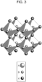
- FIG. 3 depicts an example of a perovskite material with a 3D structure of ABX 3 .
- the A cations may be larger than the B cations.
- the B cations may be in 6-fold coordination with surrounding X anions.
- the A anions may be in 12-fold coordination with surrounding X anions.
- Perovskite materials are becoming increasingly attractive for application in optoelectronic devices. Many of the perovskite materials used to make such devices are earth-abundant and relatively inexpensive, so perovskite optoelectronic devices have the potential for cost advantages. There are many classes of perovskite material. One class of perovskite material that has shown particular promise for optoelectronic devices is the metal halide perovskite material class.
- the A component may be a monovalent organic cation, such as methylammonium (CH 3 NH 3 + ) or formamidinium (CH(NH 2 ) 2 + ), an inorganic atomic cation, such as caesium (Cs + ), or a combination thereof
- the B component may be a divalent metal cation, such as lead (Pb + ), tin (Sn + ), copper (Cu + ), europium (Eu + ) or a combination thereof
- the X component may be a halide anion, such as I - , Br - , CI - , or a combination thereof.
- the perovskite material may be defined as an organic metal halide perovskite material.
- CH 3 NH 3 PbBr 3 and CH(NH 2 ) 2 PbI 3 are non-limiting examples of metal halide perovskite materials with a 3D structure.
- the perovskite material may be defined as an inorganic metal halide perovskite material.
- CsPbI 3 , CsPbCl 3 and CsPbBr 3 are non-limiting examples of inorganic metal halide perovskite materials.
- perovskite further includes any material that may adopt a layered structure of L 2 (ABX 3 ) n-1 BX 4 (which may also be written as L 2 A n-1 B n X 3n+1 ), where L, A and B are cations, X is an anion, and n is the number of BX 4 monolayers disposed between two layers of cation L.
- FIG. 4 depicts examples of perovskite materials with a layered structure of L 2 (ABX 3 ) n-1 BX 4 having different values for n.
- the A component may be a monovalent organic cation, such as methylammonium (CH 3 NH 3 + ) or formamidinium (CH(NH 2 ) 2 + ), an atomic cation, such as caesium (Cs + ), or a combination thereof
- the L component may be an organic cation such as 2-phenylethylammonium (C 6 H 5 C 2 H 4 NH 3 + ) or 1-napthylmethylammonium (C 10 H 7 CH 2 NH 3 + )
- the B component may be a divalent metal cation, such as lead (Pb + ), tin (Sn + ), copper (Cu + ), europium (Eu + ) or a combination thereof
- the X component may be a halide anion, such as I - , Br - , Cl - , or a combination thereof.
- perovskite material with a layered structure of L 2 (ABX 3 ) n-1 BX 4 adopts a structure that is approximately equivalent to perovskite material with a 3D structure of ABX 3 .
- perovskite material with a layered structure of L 2 (ABX 3 ) n-1 BX 4 adopts a two-dimensional (2D) structure of L 2 BX 4 .
- Perovskite material having a single layer may be referred to as a 2D perovskite material.
- n is small, for example n in the range of approximately 2-10
- perovskite material with a layered structure of L 2 (ABX 3 ) n-1 BX 4 adopts a quasi-two-dimensional (Quasi-2D) structure.
- Perovskite material having a small number of layers may be referred to as a Quasi-2D perovskite material. Owing to quantum confinement effects, the energy band gap is lowest for layered perovskite material structures where n is highest.
- Perovskite material may have any number of layers.
- Perovskites may comprise 2D perovskite material, Quasi-2D perovskite material, 3D perovskite material or a combination thereof.
- perovskites may comprise an ensemble of layered perovskite materials having different numbers of layers.
- perovskites may comprise an ensemble of Quasi-2D perovskite materials having different numbers of layers.
- perovskite further includes films of perovskite material.
- Films of perovskite material may be crystalline, polycrystalline or a combination thereof, with any number of layers and any range of grain or crystal size.
- perovskite further includes nanocrystals of perovskite material that have structure equivalent to or resembling the 3D perovskite structure of ABX 3 or the more general layered perovskite structure of L 2 (ABX 3 ) n-1 BX 4 .
- Nanocrystals of perovskite material may include perovskite nanoparticles, perovskite nanowires, perovskite nanoplatelets, or a combination thereof. Nanocrystals of perovskite material may be of any shape or size, with any number of layers and any range of grain or crystal sizes.
- the term "resembles" is used because for a nanocrystal of perovskite material, the distribution of L cations may differ from that of perovskite material with a formal layered structure of L 2 (ABX 3 ) n-1 BX 4 .
- perovskite material may be stimulated to emit light in response to optical or electrical excitation. That is to say that perovskite light emitting material may be photoluminescent or electroluminescent. This nomenclature may differ slightly from that used by other sources.
- perovskite light emitting material that emits red light is methylammonium lead iodide (CH 3 NH 3 Pbl 3 ).
- perovskite light emitting material that emits green light
- formamidinium lead bromide CH(NH 2 ) 2 PbBr 3
- a perovskite light emitting material that emits blue light is methylammonium lead chloride (CH 3 NH 3 PbCl 3 ).
- PeLED devices may be photoluminescent or electroluminescent.
- the term “PeLED” may be used to describe single emissive unit electroluminescent devices that comprise electroluminescent perovskite light emitting material.
- the term “PeLED” may also be used to describe one or more emissive units of stacked electroluminescent devices that comprise electroluminescent perovskite light emitting material. This nomenclature may differ slightly from that used by other sources.
- top means furthest away from the substrate, while “bottom” means closest to the substrate.
- bottom means closest to the substrate.
- first layer is described as “disposed over” a second layer, the first layer is disposed further away from the substrate. There may be other layers between the first and second layer, unless it is specified that the first layer is "in contact with” the second layer.
- solution processible means capable of being dissolved, dispersed or transported in and/or deposited from a liquid medium, either in solution or suspension form.
- a first "Highest Occupied Molecular Orbital” (HOMO) or “Lowest Unoccupied Molecular Orbital” (LUMO) energy level is “greater than” or “higher than” a second HOMO or LUMO energy level if the first energy level is closer to the vacuum energy level. Since ionization potentials (IP) and electron affinities (EA) are measured as negative energies relative to a vacuum level, a higher HOMO energy level corresponds to an IP that is less negative. Similarly, a higher LUMO energy level corresponds to an EA that is less negative.
- IP ionization potentials
- EA electron affinities
- the LUMO energy level of a material is higher than the HOMO energy level of the same material.
- a "higher” HOMO or LUMO energy level appears closer to the top of such a diagram than a "lower” HOMO or LUMO energy level.
- a first work function is "greater than” or “higher than” a second work function if the first work function has a higher absolute value. Because work functions are generally measured as negative numbers relative to vacuum level, this means that a "higher” work function is more negative. On a conventional energy level diagram, with the vacuum level at the top, a “higher” work function is illustrated as further away from the vacuum level in the downward direction. The definitions of HOMO and LUMO energy levels therefore follow a different convention than work functions.
- a light emitting device such as a PeLED, OLED or QLED may be referred to as a "stacked" light emitting device if two or more emissive units are separated by one or more charge generation layers within the layer structure of the light emitting device.
- a stacked light emitting device may be referred to as a tandem light emitting device. It should be understood that the terms “stacked” and “tandem” may be used interchangeably, and as used herein, a tandem light emitting device is also considered to be a stacked light emitting device. This nomenclature may differ slightly from that used by other sources.
- OLED organic light emitting diode
- QLED quantum and perovskite light emitting diode
- PeLED may be used to describe single emissive unit electroluminescent devices that respectively comprise electroluminescent organic, quantum and perovskite light emitting materials.
- OLED organic light emitting diode
- QLED quantum dot and perovskite light emitting materials
- PeLED may also be used to describe one or more emissive units of stacked electroluminescent devices that respectively comprise electroluminescent organic, quantum dot and perovskite light emitting materials.
- the term "optically coupled” refers to one or more elements of a device or structure that are arranged such that light may impart between the one or more elements.
- the one or more elements may be in contact or may be separated by a gap or any connection, coupling, link or the like that allows for imparting of light between the one or more elements.
- one or more sub-pixels within a pixel arrangement of a display may be optically coupled to one or more colour altering layers such as colour conversion layers and colour filters.
- the invention is as defined in claim 1.
- the device comprises a stacked blue light emitting device comprising: a first electrode; a second electrode; a first emissive unit comprising a first emissive layer; a second emissive unit comprising a second emissive layer; and a first charge generation layer; wherein the first emissive unit, the second emissive unit and the first charge generation layer are all disposed between the first electrode and the second electrode; the first emissive unit is disposed over the first electrode; the first charge generation layer is disposed over the first emissive unit; the second emissive unit is disposed over the first charge generation layer; the second electrode is disposed over the second emissive unit; the first emissive unit emits blue light having a peak wavelength in the visible spectrum in the range of 380 nm to 500 nm that is defined as the first peak wavelength; the first emissive unit emits blue light having first CIE 1931 (x, y) colour space chromaticity coordinates
- the second chromaticity coordinates (x2, y2) are not contained within a one-step MacAdam ellipse that is centralized on the first chromaticity coordinates (x1, y1). In one embodiment, the second chromaticity coordinates (x2, y2) are not contained within a three-step MacAdam ellipse that is centralized on the first chromaticity coordinates (x1, y1). In one embodiment, the second peak wavelength is at least 4 nm greater than or at least 4 nm less than the first peak wavelength.
- the first CIE 1931 (x, y) colour space chromaticity coordinates (x1, y1) may be converted to first CIE 1976 (u', v') colour space chromaticity coordinates (u1, v1); and the second CIE 1931 (x, y) colour space chromaticity coordinates (x2, y2) may be converted to second CIE 1976 (u', v') colour space chromaticity coordinates (u2, v2); wherein the first chromaticity coordinates (u1, v1) and the second chromaticity coordinates (u2, v2) are sufficiently different such that the difference in chromaticity as defined by ⁇ uv is 0.010 or more.
- the first emissive unit emits blue light with a peak wavelength in the visible spectrum in the range of 380 nm to 465 nm; and the second emissive unit emits blue light with a peak wavelength in the visible spectrum in the range of 465 nm to 500 nm.
- the first emissive unit emits blue light with a peak wavelength in the visible spectrum in the range of 465 nm to 500 nm; and the second emissive unit emits blue light with a peak wavelength in the visible spectrum in the range of 380 nm to 465 nm.
- the first emissive unit emits blue light with a CIE 1931 y coordinate of 0.080 or less; and the second emissive unit emits blue light with a CIE 1931 y coordinate of more than 0.080. In one embodiment, the first emissive unit emits blue light with a CIE 1931 y coordinate of more than 0.080; and the second emissive unit emits blue light with a CIE 1931 y coordinate of 0.080 or less.
- the first emissive layer and the second emissive layer comprise organic light emitting material. In one embodiment, at least one of the first emissive layer and the second emissive layer comprise phosphorescent organic light emitting material; and at least one of the first emissive layer and the second emissive layer comprise fluorescent organic light emitting material. In one embodiment, the first emissive layer and the second emissive layer comprise quantum dot light emitting material. In one embodiment, the first emissive layer and the second emissive layer comprise perovskite light emitting material.
- the first emissive layer comprises a first class of light emitting material that is either organic light emitting material, quantum dot light emitting material or perovskite light emitting material;
- the second emissive layer comprises a second class of light emitting material that is either organic light emitting material, quantum dot light emitting material or perovskite light emitting material; and the second class of light emitting material is not the same as the first class of light emitting material.
- first emissive unit and the second emissive unit are independently addressable and may emit light independently of each other. In one embodiment, the first emissive unit and the second emissive unit are commonly addressable and may not emit light independently of each other.
- the stacked blue light emitting device further comprises: a third emissive unit comprising a third emissive layer; and a second charge generation layer; wherein the third emissive unit and the second charge generation layer are disposed between the second emissive unit and the second electrode; the second charge generation layer is disposed over the second emissive unit; the third emissive unit is disposed over the second charge generation layer; the second electrode is disposed over the third emissive unit; the third emissive unit emits blue light having a peak wavelength in the visible spectrum in the range of 380 nm to 500 nm that is defined as the third peak wavelength; the third emissive unit emits blue light having first CIE 1931 (x, y) colour space chromaticity coordinates of (x3, y3); and the third emissive layer comprises organic light emitting material, quantum dot light emitting material or perovskite light emitting material.
- the third chromaticity is substantially the same as one of the first chromaticity and the second chromaticity; and the third chromaticity is substantially different to one of the first chromaticity and the second chromaticity.
- the third emissive unit is commonly addressed with one of the first emissive unit and the second emissive unit and may not emit light independently of one of the first emissive unit and the second emissive unit; and the third emissive unit is addressed independently of one of the first emissive unit and the second emissive unit and may emit light independently of one of the first emissive unit and the second emissive unit.
- the third emissive unit is commonly addressed with one of the first emissive unit and the second emissive unit and may not emit light independently of one of the first emissive unit and the second emissive unit; the third emissive unit is addressed independently of one of the first emissive unit and the second emissive unit and may emit light independently of one of the first emissive unit and the second emissive unit; wherein the emissive unit which is commonly addressed with the third emissive unit has substantially the same chromaticity as the third emissive unit; and the emissive unit which is addressed independently of the third emissive unit has substantially different chromaticity to the third emissive unit.
- the device is part of a light panel. In one embodiment, the device is part of a display.
- the display comprises: a first sub-pixel configured to emit red light with a peak wavelength in the visible spectrum in the range of 580 nm to 780 nm; a second sub-pixel configured to emit green light with a peak wavelength in the visible spectrum in the range of 500 nm to 580 nm; and a third sub-pixel configured to emit blue light with a peak wavelength in the visible spectrum in the range of 380 nm to 500 nm; wherein the first sub-pixel comprises a first stacked blue light emitting device optically coupled to a red colour conversion layer; the second sub-pixel comprises a second stacked blue light emitting device optically coupled to a green colour conversion layer; and the third sub-pixel comprises a third stacked blue light emitting device; wherein all of the first, second and third stacked blue light emitting devices comprise: a first electrode; a second electrode; a first emissive unit comprising a first emissive layer; a second emissive unit comprising a second
- the second chromaticity coordinates (x2, y2) are not contained within a one-step MacAdam ellipse that is centralized on the first chromaticity coordinates (x1, y1). In one embodiment, for all of the first, second and third stacked blue light emitting devices, the second chromaticity coordinates (x2, y2) are not contained within a three-step MacAdam ellipse that is centralized on the first chromaticity coordinates (x1, y1). In one embodiment, for all of the first, second and third stacked blue light emitting devices, the second peak wavelength is at least 4 nm greater than or at least 4 nm less than the first peak wavelength.
- the first CIE 1931 (x, y) colour space chromaticity coordinates (x1, y1) may be converted to first CIE 1976 (u', v') colour space chromaticity coordinates (u1, v1); and the second CIE 1931 (x, y) colour space chromaticity coordinates (x2, y2) may be converted to second CIE 1976 (u', v') colour space chromaticity coordinates (u2, v2); wherein the first chromaticity coordinates (u1, v1) and the second chromaticity coordinates (u2, v2) are sufficiently different such that the difference in chromaticity as defined by ⁇ uv is 0.010 or more.
- the first emissive unit emits blue light with a peak wavelength in the visible spectrum in the range of 380 nm to 465 nm; and the second emissive unit emits blue light with a peak wavelength in the visible spectrum in the range of 465 nm to 500 nm.
- the first emissive unit emits blue light with a peak wavelength in the visible spectrum in the range of 465 nm to 500 nm; and the second emissive unit emits blue light with a peak wavelength in the visible spectrum in the range of 380 nm to 465 nm.
- the first emissive unit emits blue light with a CIE 1931 y coordinate of 0.080 or less; and the second emissive unit emits blue light with a CIE 1931 y coordinate of more than 0.080. In one embodiment, for all of the first, second and third stacked blue light emitting devices, the first emissive unit emits blue light with a CIE 1931 y coordinate of more than 0.080; and the second emissive unit emits blue light with a CIE 1931 y coordinate of 0.080 or less.
- the first emissive layer and the second emissive layer comprise organic light emitting material. In one embodiment, for all of the first, second and third stacked blue light emitting devices, at least one of the first emissive layer and the second emissive layer comprise phosphorescent organic light emitting material; and at least one of the first emissive layer and the second emissive layer comprise fluorescent organic light emitting material. In one embodiment, for all of the first, second and third stacked blue light emitting devices, the first emissive layer and the second emissive layer comprise quantum dot light emitting material.
- the first emissive layer and the second emissive layer comprise perovskite light emitting material.
- the first emissive layer comprises a first class of light emitting material that is either organic light emitting material, quantum dot light emitting material or perovskite light emitting material;
- the second emissive layer comprises a second class of light emitting material that is either organic light emitting material, quantum dot light emitting material or perovskite light emitting material; and the second class of light emitting material is not the same as the first class of light emitting material.
- the first stacked blue light emitting device, the second stacked blue light emitting device and the third stacked blue light emitting device all have the same device architecture.
- the first emissive unit and the second emissive units are independently addressable and may emit light independently of each other. In one embodiment, for any of the first, second and third stacked blue light emitting devices, the first emissive unit and the second emissive units are commonly addressable and may not emit light independently of each other.
- the first emissive unit and the second emissive units are independently addressable and may emit light independently of each other. In one embodiment, for all of the first, second and third stacked blue light emitting devices, the first emissive unit and the second emissive units are commonly addressable and may not emit light independently of each other.
- the first emissive unit and the second emissive unit of the third stacked blue light emitting device are independently addressable and may emit light independently of each other; and the first emissive unit and the second emissive unit of the first stacked blue light emitting device are commonly addressable and may not emit light independently of each other; and the first emissive unit and the second emissive unit of the second stacked blue light emitting device are commonly addressable and may not emit light independently of each other.
- all of the first, second and third stacked blue light emitting devices further comprise: a third emissive unit comprising a third emissive layer; and a second charge generation layer; wherein the third emissive unit and the second charge generation layer are disposed between the second emissive unit and the second electrode; the second charge generation layer is disposed over the second emissive unit; the third emissive unit is disposed over the second charge generation layer; and the second electrode is disposed over the third emissive unit; and the third emissive unit emits blue light having a peak wavelength in the visible spectrum in the range of 380 nm to 500 nm that is defined as the third peak wavelength; the third emissive unit emits blue light having a third chromaticity having third CIE 1931 (x, y) colour space chromaticity coordinates of (x3, y3); and the third emissive layer comprises organic light emitting material, quantum dot light emitting material or perovskite light emitting material.
- the third chromaticity is substantially the same as one of the first chromaticity and the second chromaticity; and the third chromaticity is substantially different to one of the first chromaticity and the second chromaticity.
- the third emissive unit is commonly addressed with one of the first emissive unit and the second emissive unit and may not emit light independently of one of the first emissive unit and the second emissive unit; and the third emissive unit is addressed independently of one of the first emissive unit and the second emissive unit and may emit light independently of one of the first emissive unit and the second emissive unit.
- the third emissive unit is commonly addressed with one of the first emissive unit and the second emissive unit and may not emit light independently of one of the first emissive unit and the second emissive unit; the third emissive unit is addressed independently of one of the first emissive unit and the second emissive unit and may emit light independently of one of the first emissive unit and the second emissive unit; wherein the emissive unit which is commonly addressed with the third emissive unit has substantially the same chromaticity as the third emissive unit; and the emissive unit which is addressed independently of the third emissive unit has substantially different chromaticity to the third emissive unit.
- the display is part of a consumer product.
- an underlined number is employed to represent an item over which the underlined number is positioned or an item to which the underlined number is adjacent.
- a non-underlined number relates to an item identified by a line linking the non-underlined number to the item.
- the non-underlined number is used to identify a general item at which the arrow is pointing.
- the present invention relates to OLEDs, QLEDs and PeLEDs.
- Device architectures and operating principles for OLEDs, QLEDs and PeLEDs are substantially similar.
- Each of these light emitting devices comprises at least one emissive layer disposed between and electrically connected to an anode and a cathode.
- the emissive layer comprises organic light emitting material.
- the emissive layer comprises quantum dot light emitting material.
- the emissive layer comprises perovskite light emitting material. For each of these light emitting devices, when a current is applied, the anode injects holes and the cathode injects electrons into the emissive layer(s).
- the injected holes and electrons each migrate towards the oppositely charged electrode.
- an exciton which is a localized electron-hole pair having an excited energy state, may be formed.
- Light is emitted if the exciton relaxes via a photo-emissive mechanism.
- Non-radiative mechanisms such as thermal radiation and/or Auger recombination may also occur but are generally considered undesirable.
- Substantial similarity between device architectures and working principles required for OLEDs, QLEDs and PeLEDs facilitates the combination of organic light emitting material, quantum dot light emitting material and perovskite light emitting material in a single light emitting device.
- FIG. 1 shows a light emitting device 100, not forming part of the claimed invention, with a single emissive unit.
- the light emitting device 100 may be an OLED, QLED or PeLED.
- Device 100 may include a substrate 110, an anode 115, a hole injection layer 120, a hole transport layer 125, an electron blocking layer 130, an emissive layer 135, a hole blocking layer 140, an electron transport layer 145, an electron injection layer 150, a cathode 155 and a barrier layer 160.
- Device 100 may be fabricated by depositing the layers described in order. As the device 100 has anode 115 disposed under cathode 155, device 100 may be referred to as a "standard" device architecture.
- the emissive layer comprises organic light emitting material.
- the emissive layer comprises quantum dot light emitting material.
- the emissive layer comprises perovskite light emitting material.
- FIG. 2 shows an inverted light emitting device 200, not forming part of the claimed invention, with a single emissive unit.
- the light emitting device 200 may be an OLED, QLED or PeLED.
- the device includes a substrate 210, a cathode 215, an emissive layer 220, a hole transport layer 225, and an anode 230.
- Device 200 may be fabricated by depositing the layers described in order. As the device 200 has cathode 215 disposed under anode 230, device 200 may be referred to as an "inverted" device architecture.
- the emissive layer comprises organic light emitting material.
- the emissive layer comprises quantum dot light emitting material.
- the emissive layer comprises perovskite light emitting material. Materials similar to those described with respect to device 100 may be used in the corresponding layers of device 200.
- FIG. 2 provides one example of how some layers may be omitted from the structure of an OLED, QLED or PeLED.
- FIGS. 1 and 2 The simple layered structures illustrated in FIGS. 1 and 2 are provided by way of non-limiting examples, and it is understood that embodiments of the invention may be used in connection with a wide variety of other structures.
- the specific materials and structures described are exemplary in nature, and other materials and structures may be used.
- Functional OLEDs, QLEDs and PeLEDs may be achieved by combining the various layers described in different ways, or layers may be omitted entirely, based on factors such as performance, design and cost. Other layers, not specifically described, may also be included. Materials other than those specifically described may be used. Although many of the examples provided herein describe various layers as comprising a single material, it is understood that combinations of materials may be used. Also, the layers may have various sublayers. The names given to the various layers herein are not intended to be strictly limiting. For example, in a device, the hole transport layer may transport and inject holes into the emissive layer and may be described as a hole transport layer or a hole injection layer.
- OLEDs, PeLEDs and QLEDs are generally intended to emit light through at least one of the electrodes, and one or more transparent electrodes may be useful in such optoelectronic devices.
- a transparent electrode material such as indium tin oxide (ITO)
- ITO indium tin oxide
- Mg:Ag thin metallic layer of a blend of magnesium and silver
- the top electrode does not need to be transparent, and may be comprised of an opaque and/or reflective layer, such as a metal layer having a high reflectivity.
- the bottom electrode may be opaque and/or reflective, such as a metal layer having a high reflectivity.
- a metal layer having a high reflectivity may be opaque and/or reflective, such as a metal layer having a high reflectivity.
- using a thicker layer may provide better conductivity and may reduce voltage drop and/or Joule heating in the device, and using a reflective electrode may increase the amount of light emitted through the other electrode by reflecting light back towards the transparent electrode.
- a fully transparent device may also be fabricated, where both electrodes are transparent.
- the substrate 110 may comprise any suitable material that provides the desired structural and optical properties.
- the substrate 110 may be rigid or flexible.
- the substrate 110 may be flat or curved.
- the substrate 110 may be transparent, translucent or opaque.
- Preferred substrate materials are glass, plastic and metal foil. Other substrates, such as fabric and paper may be used.
- the material and thickness of the substrate 110 may be chosen to obtain desired structural and optical properties.
- the anode 115 may comprise any suitable material or combination of materials known to the art, such that the anode 115 is capable of conducting holes and injecting them into the layers of the device.
- Preferred anode 115 materials include conductive metal oxides, such as indium tin oxide (ITO), indium zinc oxide (IZO) and aluminum zinc oxide (AlZnO), metals such as silver (Ag), aluminum (Al), aluminum-neodymium (AI:Nd), gold (Au) and alloys thereof, or a combination thereof.
- Other preferred anode 115 materials include graphene, carbon nanotubes, nanowires or nanoparticles, silver nanowires or nanoparticles, organic materials, such as poly(3,4-ethylenedioxythiophene) : polystyrene sulfonate (PEDOT:PSS) and derivatives thereof, or a combination thereof.
- Compound anodes comprising one or more anode materials in a single layer may be preferred for some devices.
- Multilayer anodes comprising one or more anode materials in one or more layers may be preferred for some devices.
- One example of a multilayer anode is ITO/Ag/ITO.
- the anode 115 may be sufficiently transparent to create a bottom-emitting device, where light is emitted through the substrate.
- a transparent anode commonly used in a standard device architecture is a layer of ITO.
- ITO/Ag/ITO is another example of a transparent anode commonly used in a standard device architecture, where the Ag thickness is less than approximately 25 nm.
- the anode may be transparent as well as partially reflective.
- a microcavity may provide one or more of the following advantages: an increased total amount of light emitted from device, and therefore higher efficiency and brightness; an increased proportion of light emitted in the forward direction, and therefore increased apparent brightness at normal incidence; and spectral narrowing of the emission spectrum, resulting in light emission with increased colour saturation.
- the anode 115 may be opaque and/or reflective.
- a reflective anode 115 may be preferred for some top-emitting devices to increase the amount of light emitted from the top of the device.
- a reflective anode commonly used in a standard device architecture is a multilayer anode of ITO/Ag/ITO, where the Ag thickness is greater than approximately 80 nm.
- a transparent and partially reflective cathode such as Mg:Ag
- Mg:Ag transparent and partially reflective cathode
- the material and thickness of the anode 115 may be chosen to obtain desired conductive and optical properties. Where the anode 115 is transparent, there may be a range of thicknesses for a particular material that is thick enough to provide the desired conductivity, yet thin enough to provide the desired degree of transparency. Other materials and structures may be used.
- Devices fabricated in accordance with embodiments of the present invention may optionally comprise a hole transport layer 125.
- the hole transport layer 125 may include any material capable of transporting holes.
- the hole transport layer 125 may be deposited by a solution process or by a vacuum deposition process.
- the hole transport layer 125 may be doped or undoped. Doping may be used to enhance conductivity.
- Examples of undoped hole transport layers are N,N'-Di(1-naphthyl)-N,N'-diphenyl-(1,1'-biphenyl)-4,4'-diamine (NPD), poly[(9,9-dioctylfluorenyl-2,7-diyl)-co -(4,4'-(N -(4-sec-butylphenyl) diphenylamine (TFB), poly[N,N'-bis(4-butylphenyl)-N,N'-bis(phenyl)-benzidine] (poly-TPD), poly(9-vinylcarbazole) (PVK), 4,4'-Bis(N-carbazolyl)-1,1'-biphenyl (CBP), Spiro-OMeTAD and molybdenum oxide (MoO 3 ).
- NPD N,N'-Di(1-naphthyl)
- a doped hole transport layer is 4,4',4"-tris[phenyl(m-tolyl)amino]triphenylamine (m-MTDATA) doped with F 4 -TCNQ at a molar ratio of 50:1.
- m-MTDATA 4,4',4"-tris[phenyl(m-tolyl)amino]triphenylamine
- F 4 -TCNQ F 4 -TCNQ at a molar ratio of 50:1.
- m-MTDATA 4,4',4"-tris[phenyl(m-tolyl)amino]triphenylamine
- F 4 -TCNQ F 4 -TCNQ at a molar ratio of 50:1.
- PEDOT:PSS PEDOT:PSS.
- Other hole transport layers and structures may be used.
- Devices fabricated in accordance with embodiments of the present invention may optionally comprise an emissive layer 135.
- the emissive layer 135 may include any material capable of emitting light when a current is passed between anode 115 and cathode 155.
- perovskite light-emitting materials include 3D perovskite materials, such as methylammonium lead iodide (CH 3 NH 3 PbI 3 ), methylammonium lead bromide (CH 3 NH 3 PbBr 3 ), methylammonium lead chloride (CH 3 NH 3 PbCl 3 ), formamidinium lead iodide (CH(NH 2 ) 2 PbI 3 ), formamidinium lead bromide (CH(NH 2 ) 2 PbBr 3 ), formamidinium lead chloride (CH(NH 2 ) 2 PbCl 3 ), caesium lead iodide (CsPbI 3 ), caesium lead bromide (CsPbBr 3 ) and caesium lead chloride (CsPbCl 3 ).
- 3D perovskite materials such as methylammonium lead iodide (CH 3 NH 3 PbI 3 ), methylammonium lead
- perovskite light-emitting materials further include 3D perovskite materials with mixed halides, such as CH 3 NH 3 PbI 3-x Cl x , CH 3 NH 3 PbI 3-x Br x , CH 3 NH 3 PbCl 3-X Br X , CH(NH 2 ) 2 PbI 3-x Br x , CH(NH 2 ) 2 PbI 3-x Cl x , CH(NH 2 ) 2 PbCl 3-x Br x , CsPbI 3-x Cl x , CsPbI 3-x Br x and CsPbCl 3-x Br x , where x is in the range of 0-3.
- 3D perovskite materials with mixed halides such as CH 3 NH 3 PbI 3-x Cl x , CH 3 NH 3 PbI 3-x Br x , CH 3 NH 3 PbCl 3-X Br X , CH(NH 2 ) 2 PbI 3-x Br x ,
- perovskite light-emitting materials further include 2D perovskite materials such as (C 10 H 7 CH 2 NH 3 ) 2 PbI 4 , (C1 0 H 7 CH 2 NH 3 ) 2 PbBr 4 , (C 10 H 7 CH 2 NH 3 ) 2 PbCl 4 , (C 6 H 5 C 2 H 4 NH 3 ) 2 PbI 4 , (C 6 H 5 C 2 H 4 NH 3 ) 2 PbBr 4 and (C 6 H 5 C 2 H 4 NH 3 ) 2 PbCl 4 , 2D perovskite materials with mixed halides, such as (C 10 H 7 CH 2 NH 3 ) 2 PbI 4-x Cl x , (C 10 H 7 CH 2 NH 3 ) 2 PbI 4-x Br x , (C 10 H 7 CH 2 NH 3 ) 2 PbCl 4-x Br x , (C 6 H 5 C 2 H 4 NH 3 ) 2 PbI 4-x
- perovskite light-emitting materials further include Quasi-2D perovskite materials, such as (C 6 H 5 C 2 H 4 NH 3 ) 2 (CH(NH 2 ) 2 PbBr 3 ) n-1 PbI 4 , (C 6 H 5 C 2 H 4 NH 3 ) 2 (CH(NH 2 ) 2 PbBr 3 ) n-1 PbBr 4 , (C 6 H 5 C 2 H 4 NH 3 ) 2 (CH(NH 2 ) 2 PbBr 3 ) n-1 PbCl 4 , (C 10 H 7 CH 2 NH 3 ) 2 (CH 3 NH 3 PbI 2 Br) n-1 PbI 4 , (C 10 H 7 CH 2 NH 3 ) 2 (CH 3 NH 3 PbI 2 Br) n-1 PbBr 4 and (C 10 H 7 CH 2 NH 3 ) 2 (CH 3 NH 3 PbI 2 Br) n-1 PbCl 4 , where n
- perovskite light-emitting materials further include Quasi-2D perovskite materials with mixed halides, such as (C 6 H 5 C 2 H 4 NH 3 ) 2 (CH(NH 2 ) 2 PbBr 3 ) n-1 PbI 4-x Cl x , (C 6 H 5 C 2 H 4 NH 3 ) 2 (CH(NH 2 ) 2 PbBr 3 ) n-1 PbI 4-x Br x , (C 6 H 5 C 2 H 4 NH 3 ) 2 (CH(NH 2 ) 2 PbBr 3 ) n-1 PbCl 4-x Br x , (C 10 H 7 CH 2 NH 3 ) 2 (CH 3 NH 3 PbI 2 Br) n-1 PbI 4-x Cl x , (C 10 H 7 CH 2 NH 3 ) 2 (CH 3 NH 3 PbI 2 Br) n-1 PbI 4-x Cl x , (C 10 H 7 CH 2 NH 3 ) 2 (CH
- perovskite light-emitting materials further include any of the aforementioned examples, where the divalent metal cation lead (Pb + ) may be replaced with tin (Sn + ), copper (Cu + ) or europium (Eu + ).
- Examples of perovskite light-emitting materials further include perovskite light-emitting nanocrystals with structures that closely resemble Quasi-2D perovskite materials.
- Perovskite light emitting material may comprise organic metal halide perovskite material, such as methylammonium lead iodide (CH 3 NH 3 PbI 3 ), methylammonium lead bromide (CH 3 NH 3 PbBr 3 ), methylammonium lead chloride (CH 3 NH 3 PbCl 3 ), where the materials comprises an organic cation.
- organic metal halide perovskite material such as methylammonium lead iodide (CH 3 NH 3 PbI 3 ), methylammonium lead bromide (CH 3 NH 3 PbBr 3 ), methylammonium lead chloride (CH 3 NH 3 PbCl 3 ), where the materials comprises an organic cation.
- Perovskite light emitting material may comprise inorganic metal halide perovskite material, such as caesium lead iodide (CsPbI 3 ), caesium lead bromide (CsPbBr 3 ) and caesium lead chloride (CsPbCl 3 ), where the material comprises an inorganic cation.
- perovskite light emitting material may comprise perovskite light emitting material where there is a combination of organic and inorganic cations. The choice of an organic or inorganic cation may be determined by several factors, including desired emission colour, efficiency of electroluminescence, stability of electroluminescence and ease of processing.
- Inorganic metal halide perovskite material may be particularly well-suited to perovskite light-emitting materials with a nanocrystal structure, such as those depicted in FIG. 5 , wherein an inorganic cation may enable a compact and stable perovskite light-emitting nanocrystal structure.
- Perovskite light emitting material may be included in the emissive layer 135 in a number of ways.
- the emissive layer may comprise 2D perovskite light-emitting material, Quasi-2D perovskite light-emitting material or 3D perovskite light-emitting material, or a combination thereof.
- the emissive layer may comprise perovskite light emitting nanocrystals.
- the emissive layer 135 may comprise an ensemble of Quasi-2D perovskite light emitting materials, where the Quasi-2D perovskite light emitting materials in the ensemble may comprise a different number of layers.
- An ensemble of Quasi-2D perovskite light emitting materials may be preferred because there may be energy transfer from Quasi-2D perovskite light emitting materials with a smaller number of layers and a larger energy band gap to Quasi-2D perovskite light emitting materials with a larger number of layers and a lower energy band gap.
- This energy funnel may efficiently confine excitons in a PeLED device and may improve device performance.
- the emissive layer 135 may comprise perovskite light emitting nanocrystal materials.
- Perovskite light emitting nanocrystal materials may be preferred because nanocrystal boundaries may be used to confine excitons in a PeLED device, and surface cations may be used to passivate the nanocrystal boundaries. This exciton confinement and surface passivation may improve device performance.
- Other emissive layer materials and structures may be used.
- Devices fabricated in accordance with embodiments of the present invention may optionally comprise an electron transport layer 145.
- the electron transport layer 145 may include any material capable of transporting electrons.
- the electron transport layer 145 may be deposited by a solution process or by a vacuum deposition process.
- the electron transport layer 145 may be doped or undoped. Doping may be used to enhance conductivity.
- Examples of undoped electron transport layers are tris(8-hydroxyquinolinato)aluminum (Alq 3 ), 2,2',2"-(1,3,5-Benzinetriyl)-tris(1-phenyl-1-H-benzimidazole) (TPBi), 2,9-Dimethyl-4,7-diphenyl-1,10-phenanthroline (BCP), zinc oxide (ZnO) and titanium dioxide (TiOs).
- One example of a doped electron transport layer is 4,7-diphenyl-1,10-phenanthroline (BPhen) doped with lithium (Li) at a molar ratio of 1:1.
- BPhen 4,7-diphenyl-1,10-phenanthroline
- Li lithium
- a solution-processed electron transport layer is [6,6]-Phenyl C61 butyric acid methyl ester (PCBM).
- PCBM solution-processed electron transport layer
- Other electron transport layers and structures may be used.
- the cathode 155 may comprise any suitable material or combination of materials known to the art, such that the cathode 155 is capable of conducting electronics and injecting them into the layers of the device.
- Preferred cathode 155 materials include metal oxides, such as indium tin oxide (ITO), indium zinc oxide (IZO) and fluorine tin oxide (FTO), metals, such as calcium (Ca), barium (Ba), magnesium (Mg) and ytterbium (Yb) or a combination thereof.
- cathode 155 materials include metals such as silver (Ag), aluminum (Al), aluminum-neodymium (Al: Nd), gold (Au) and alloys thereof, or a combination thereof.
- Compound cathodes comprising one or more cathode materials in a single layer may be preferred from some devices.
- One example of a compound cathode is Mg:Ag.
- Multilayer cathodes comprising one or more cathode materials in one or more layers may be preferred for some devices.
- a multilayer cathode is Ba/AI.
- the cathode 155 may be sufficiently transparent to create a top-emitting device, where light is emitted from the top of the device.
- a transparent cathode commonly used in a standard device architecture is a compound layer of Mg:Ag.
- the cathode may be transparent as well as partially reflective.
- a reflective anode such as ITO/Ag/ITO, where the Ag thickness is greater than approximately 80 nm, this may have the advantage of creating a microcavity within the device.
- the cathode 155 may be opaque and/or reflective.
- a reflective cathode 155 may be preferred for some bottom-emitting devices to increase the amount of light emitted through the substrate from the bottom of the device.
- a reflective cathode commonly used in a standard device architecture is a multilayer cathode of LiF/AI.
- a transparent and partially reflective anode such as ITO/Ag/ITO, where the Ag thickness is less than approximately 25 nm, this may have the advantage of creating a microcavity within the device.
- the material and thickness of the cathode 155 may be chosen to obtain desired conductive and optical properties. Where the cathode 155 is transparent, there may be a range of thicknesses for a particular material that is thick enough to provide the desired conductivity, yet thin enough to provide the desired degree of transparency. Other materials and structures may be used.
- Blocking layers may be used to reduce the number of charge carriers (electrons or holes) and/or excitons exiting the emissive layer.
- An electron blocking layer 130 may be disposed between the emissive layer 135 and the hole transport layer 125 to block electrons from leaving the emissive layer 135 in the direction of the hole transport layer 125.
- a hole blocking layer 140 may be disposed between the emissive layer 135 and the electron transport layer 145 to block holes from leaving the emissive layer 135 in the direction of the electron transport layer 145.
- Blocking layers may also be used to block excitons from diffusing from the emissive layer.
- blocking layer means that the layer provides a barrier that significantly inhibits transport of charge carriers and/or excitons, without suggesting that the layer completely blocks the charge carriers and/or excitons.
- the presence of such a blocking layer in a device may result in substantially higher efficiencies as compared to a similar device lacking a blocking layer.
- a blocking layer may also be used to confine emission to a desired region of a device.
- injection layers are comprised of one or more materials that may improve the injection of charge carriers from one layer, such as an electrode, into an adjacent layer. Injection layers may also perform a charge transport function.
- the hole injection layer 120 may be any layer that improves the injection of holes from the anode 115 into the hole transport layer 125.
- Examples of materials that may be used as a hole injection layer are Copper(II)phthalocyanine (CuPc) and 1,4,5,8,9,11-Hexaazatriphenylenehexacarbonitrile (HATCN), which may be vapor deposited, and polymers, such as PEDOT:PSS, which may be deposited from solution.
- a material that may be used as a hole injection layer is molybdenum oxide (MoOs).
- a hole injection layer (HIL) 120 may comprise a charge carrying component having HOMO energy level that favourably matches, as defined by their herein-described relative IP energies, with the adjacent anode layer on one side of the HIL, and the hole transporting layer on the opposite side of the HIL.
- the "charge carrying component” is the material responsible for the HOMO energy level that actually transports the holes. This material may be the base material of the HIL, or it may be a dopant. Using a doped HIL allows the dopant to be selected for its electrical properties, and the host to be selected for morphological properties, such as ease of deposition, wetting, flexibility, toughness, and others.
- HIL material Preferred properties of the HIL material are such that holes can be efficiently injected from the anode into the HIL material.
- the charge carrying component of the HIL 120 preferably has an IP not more than about 0.5 eV greater than the IP of the anode material. Similar conditions apply to any layer into which holes are being injected.
- HIL materials are further distinguished from conventional hole transporting materials that are typically used in the hole transporting layer of an OLED, QLED or PeLED in that such HIL materials may have a hole conductivity that is substantially less than the hole conductivity of conventional hole transporting materials.
- the thickness of the HIL 120 of the present invention may be thick enough to planarize the anode and enable efficient hole injection, but thin enough not to hinder transportation of holes. For example, an HIL thickness of as little as 10 nm may be acceptable. However, for some devices, an HIL thickness of up to 50 nm may be preferred.
- the electron injection layer 150 may be any layer that improves the injection of electrons from the cathode 155 into the electron transport layer 145.
- materials that may be used as an electron injection layer are inorganic salts, such as lithium fluoride (LiF), sodium fluoride (NaF), barium fluoride (BaF), caesium fluoride (CsF), and caesium carbonate (CsCO 3 ).
- materials that may be used as an electron injection layer are metal oxides, such as zinc oxide (ZnO) and titanium oxide (TiO 2 ), and metals, such as calcium (Ca), barium (Ba), magnesium (Mg) and ytterbium (Yb).
- Other materials or combinations of materials may be used for injection layers.
- injection layers may be disposed at locations different than those shown in device 100.
- Devices fabricated in accordance with embodiments of the present invention may optionally comprise a barrier layer 160.
- One purpose of the barrier layer 160 is to protect device layers from damaging species in the environment, including moisture, vapour and/or gasses.
- the barrier layer 160 may be deposited over, under or next to the substrate, electrode, or any other parts of the device, including an edge.
- the barrier layer 160 may be a bulk material such as glass or metal, and the bulk material may be affixed over, under of next to the substrate, electrode, or any other parts of the device.
- the barrier layer 160 may be deposited onto a film, and the film may be affixed over, under of next to the substrate, electrode, or any other parts of the device.
- barrier layer 160 is deposited onto a film
- preferred film materials comprise glass, plastics, such as polyethylene terephthalate (PET) and polyethylene naphthalate (PEN) and metal foils.
- PET polyethylene terephthalate
- PEN polyethylene naphthalate
- preferred materials used to affix the film or bulk material to the device include thermal or UV-curable adhesives, hot-melt adhesives and pressure sensitive adhesives.
- the barrier layer 160 may be a bulk material or formed by various known deposition techniques, including sputtering, vacuum thermal evaporation, electron-beam deposition and chemical vapour deposition (CVD) techniques, such as plasma-enhanced chemical vapour deposition (PECVD) and atomic layer deposition (ALD).
- the barrier layer 160 may include compositions having a single phase as well as compositions having multiple phases. Any suitable material or combination of materials may be used for the barrier layer 160.
- the barrier layer 160 may incorporate organic or inorganic compounds or both.
- Preferred inorganic barrier layer materials include aluminum oxides such as Al 2 O 3 , silicon oxides such as SiOz, silicon nitrides such as SiN x and bulk materials such as glasses and metals.
- Preferred organic barrier layer materials include polymers.
- the barrier layer 160 may comprise a single layer or multiple layers.
- Multilayer barriers comprising one or more barrier materials in one or more layers may be preferred for some devices.
- One preferred example of a multilayer barrier is a barrier comprising alternating layers of SiN x and a polymer, such as in the multilayer barrier SiN x /polymer/SiN x .
- FIG. 6 shows a stacked light emitting device 600, not forming part of the claimed invention, having two emissive units.
- the light emitting device 600 may comprise one or more OLED, QLED or PeLED emissive units or a combination thereof.
- Device 600 may include a first electrode 610, a first emissive unit 620, a first charge generation layer 630, a second emissive unit 640, and a second electrode 650.
- the first electrode 610 may be directly connected to an external electrical source E1.
- the second electrode 650 may be directly connected to an external electrical source E2.
- the first charge generation layer 630 may be directly connected to an external electrical source E3.
- Device 600 may be fabricated by depositing the layers described in order.
- FIG. 8 depicts a layer structure for a stacked light emitting device 800 having two emissive units.
- the light emitting device 800 may comprise one or more OLED, QLED or PeLED emissive units or a combination thereof.
- Device 800 may include a substrate 805, an anode 810, a first hole injection layer 815, a first hole transport layer 820, a first emissive layer 825, a first hole blocking layer 830, a first electron transport layer 835, a first charge generation layer 840, a second hole injection layer 845, a second hole transport layer 850, a second emissive layer 855, a second hole blocking layer 860, a second electron transport layer 865, a first electron injection layer 870, and a cathode 875.
- the first emissive unit 880 may comprise the first hole injection layer 815, the first hole transport layer 820, the first emissive layer 825, the first hole blocking layer 830, and the first electron transport layer 835.
- the second emissive unit 885 may comprise the second hole injection layer 845, the second hole transport layer 850, the second emissive layer 855, the second hole blocking layer 860, the second electron transport layer 865, and the first electron injection layer 870.
- Device 800 may be fabricated by depositing the layers described in order.
- FIG. 7 shows a stacked light emitting device 700 having three emissive units.
- the light emitting device 700 may comprise one or more OLED, QLED or PeLED emissive units or a combination thereof.
- Device 700 may include a first electrode 710, a first emissive unit 720, a first charge generation layer 730, a second emissive unit 740, a second charge generation layer 750, a third emissive unit 760, and a second electrode 770.
- the first electrode 710 may be directly connected to an external electrical source E1.
- the second electrode 770 may be directly connected to an external electrical source E2.
- the first charge generation layer 730 may be directly connected to an external electrical source E3.
- the second charge generation layer 750 may be connected to an external electrical source E4.
- Device 700 may be fabricated by depositing the layers described in order.
- FIG. 9 depicts a layer structure for a stacked light emitting device 900 having three emissive units.
- the light emitting device 900 may comprise one or more OLED, QLED or PeLED emissive units or a combination thereof.
- Device 900 may include a substrate 905, an anode 910, a first hole injection layer 915, a first hole transport layer 920, a first emissive layer 925, a first electron transport layer 930, a first charge generation layer 935, a second hole transport layer 940, a second emissive layer 945, a second electron transport layer 950, a second charge generation layer 955, a third hole transport layer 960, a third emissive layer 965, a third electron transport layer 970, a first electron injection layer 975, and a cathode 980.
- the first emissive unit 985 may comprise the first hole injection layer 915, the first hole transport layer 920, the first emissive layer 925, and the first electron transport layer 930.
- the second emissive unit 990 may comprise the second hole transport layer 940, the second emissive layer 945, and the second electron transport layer 950.
- the third emissive unit 995 may comprise the third hole transport layer 960, the third emissive layer 965, the third electron transport layer 970, and the first electron injection layer 975.
- Device 900 may be fabricated by depositing the layers described in order.
- FIGS. 8 and 9 The simple layered structures illustrated in FIGS. 8 and 9 are provided by way of non-limiting examples, and it is understood that embodiments of the invention may be used in connection with a wide variety of other structures.
- the specific materials and structures described are exemplary in nature, and other materials and structures may be used.
- Functional light emitting devices may be achieved by combining the various layers described in different ways, or layers may be omitted entirely, based on factors such as performance, design and cost. Other layers, not specifically described, may also be included. Materials other than those specifically described may be used.
- the electron transport layer may transport electrons into the emissive layer, and also block holes from exiting the emissive layer, and may be described as an electron transport layer or a hole blocking layer.
- Stacked light emitting device architectures may provide one or more of the following advantages: (1) light from multiple emissive units may be combined within the same surface area of the device thereby increasing the brightness of the device; (2) multiple emissive units may be connected electrically in series with substantially the same current passing through each emissive unit thereby allowing the device to operate at increased brightness without substantial increase in current density thereby extending the operation lifetime of the device; and (3) the light emitted from separate emissive units may be separately controlled, thereby allowing the brightness and/or colour of the device to be tuned according to the exact needs of the application.
- stacked light emitting devices that include organic light emitting materials are described in United States patent US 5707745 B1, Forrest et al. , Fröbel et al. and Jung et al. United States patent US 5707745 B1 describes a multicolour stacked organic light emitting device. Forrest et al. and Fröbel et al. describe stacked organic light emitting devices comprising red, green and blue emissive units that are independently addressable.
- Jung et al. describes a top emitting stacked organic light emitting device comprising three emissive units, where light from the three emissive units may be combined to generate emission of white light from the device.
- the present invention relates to a stacked blue light emitting device architecture comprising two or more emissive units that emit blue light having substantially different chromaticity for application in displays, light panels and other optoelectronic devices.
- at least one emissive unit may emit a deeper blue light and at least one emissive unit may emit a lighter blue light.
- emissive units may be addressed independently and may emit light independently of each other.
- emissive units may be commonly addressed and may not emit light independently of each other.
- Such stacked blue light emitting devices may be incorporated into the red, green and blue sub-pixels of an OLED display.
- the blue sub-pixel of such a display is required to emit a relatively saturated blue light
- the emissive unit that emits deeper blue light may be individually addressed and may emit light to generate the display image while the emissive unit that emits lighter blue light may remain inactive.
- the blue sub-pixel of such a display is only required to emit a relatively unsaturated blue light
- the emissive unit that emits lighter blue light may be individually addressed and may emit light to generate the display image while the emissive unit that emits deeper blue light may remain inactive.
- Light may be emitted from the relatively more efficient and/or stable lighter blue emissive unit to render the majority of display images, with light emitted from the relatively less efficient and/or stable deeper blue emissive unit only required to render a small proportion of images.
- the efficiency and/or lifetime of the display may therefore be enhanced.
- the lighter blue emissive unit may be used on its own or in combination with the deeper blue emissive unit to provide light to the red and green colour conversion layers in the red and green sub-pixels.
- devices fabricated in accordance with embodiments of the present invention may comprise two emissive layers.
- devices fabricated in accordance with embodiments of the present invention may comprise three emissive layers.
- devices fabricated in accordance with embodiments of the present invention may comprise four or more emissive layers.
- devices fabricated in accordance with embodiments of the present invention may comprise two emissive units.
- devices fabricated in accordance with embodiments of the present invention may comprise three emissive units.
- devices fabricated in accordance with embodiments of the present invention may comprise four or more emissive units.
- an emissive unit may comprise an emissive layer.
- an emissive unit may further comprise one or more additional layers, such as a hole injection layer, a hole transport layer, an electron blocking layer, a hole blocking layer, an electron transport layer and/or an electron injection layer.
- additional layers such as a hole injection layer, a hole transport layer, an electron blocking layer, a hole blocking layer, an electron transport layer and/or an electron injection layer.
- some of these additional layers may be included within an emissive unit, and some of these additional layers may be excluded.
- Devices fabricated in accordance with embodiments of the present invention may optionally comprise one or more charge generation layers.
- a charge generation layer may be used to separate two or more emissive units within a stacked light emitting device.
- Stacked light emitting device 600 depicted in FIG. 6 and not forming part of the claimed invention, comprises a first charge generation layer 630, which separates a first emissive unit 620 from a second emissive unit 640.
- Stacked light emitting device 700 depicted in FIG. 7 , comprises a first charge generation layer 730, which separates a first emissive unit 720 from a second emissive unit 740.
- Stacked light emitting device 700 depicted in FIG. 7 , further comprises a second charge generation layer 750, which separates a second emissive unit 740 from a third emissive unit 760.
- a charge generation layer 630, 730 or 750 may comprise a single layer or multiple layers.
- a charge generation layer 630, 730 or 750 may comprise an n-doped layer for the injection of electrons, and a p-doped layer for the injection of holes.
- a charge generation layer 630, 730 or 750 may include a hole injection layer (HIL).
- HIL hole injection layer
- a p-doped layer of a charge generation layer 630, 730 or 750 may function as a hole injection layer (HIL).
- FIG. 9 depicts a stacked light emitting device 900 having three emissive units, where a first charge generation layer 935 includes a hole injection layer (not shown), and a second charge generation layer 955 includes a hole injection layer (not shown).
- a charge generation layer 630, 730 or 750 may be positioned adjacent to and in contact with a separate hole injection layer.
- FIG. 8 depicts a stacked light emitting device 800 having two emissive units, where a first charge generation layer 840 is adjacent to and in contact with a second hole injection layer 845.
- a charge generation layer 630, 730 or 750 may include an electron injection layer (EIL).
- EIL electron injection layer
- an n-doped layer of a charge generation layer 630, 730 or 750 may function as an electron injection layer (EIL).
- FIG. 9 depicts a stacked light emitting device 900 having three emissive units, where a first charge generation layer 935 includes an electron injection layer (not shown), and a second charge generation layer 955 includes an electron injection layer (not shown).
- a charge generation layer 630, 730 or 750 may be positioned adjacent to and in contact with a separate electron injection layer.
- a charge generation layer 630, 730 or 750 may include a layer for conducting holes and/or injecting them into the layers of the device. Such a layer may comprise any suitable material or combination of materials known to the art, such that the layer is capable of conducting holes and/or injecting them into the layers of the device. Such a layer may be referred to as an anode layer.
- a charge generation layer 630, 730 or 750 may include a layer for conducting electrons and/or injecting them into the layers of the device. Such a layer may comprise any suitable material or combination of materials known to the art, such that the layer is capable of conducting electrons and/or injecting them into the layers of the device. Such a layer may be referred to as a cathode layer.
- a charge generation layer 630, 730 or 750 may comprise an anode and cathode layer that are electrically connected to each other.
- a charge generation layer 630, 730 or 750 may be deposited by a solution process or by a vacuum deposition process.
- a charge generation layer 630, 730 or 750 may be composed of any applicable materials that enable injection of electrons and holes.
- a charge generation layer 630, 730 or 750 may be doped or undoped. Doping may be used to enhance conductivity.
- vapour process charge generation layer is a dual layer structure consisting of lithium doped BPhen (Li-BPhen) as the n-doped layer for electron injection, in combination with of 1,4,5,8,9,11-Hexaazatriphenylenehexacarbonitrile (HATCN) as the p-doped layer for hole injection.
- a solution process charge generation layer is a dual layer structure consisting of polyethylenimine (PEI) surface modified zinc oxide (ZnO) as the n-doped layer for electron injection, in combination with molybdenum oxide (MoOs) or tungsten trioxide (WO 3 ) as the p-doped layer for hole injection.
- PEI polyethylenimine
- ZnO surface modified zinc oxide
- MoOs molybdenum oxide
- WO 3 tungsten trioxide
- Other materials or combinations of materials may be used for charge generation layers.
- charge generation layers may be disposed at locations different than those shown in device 800 and device 900
- one or more charge generation layers within a stacked light emitting device may be directly connected to one or more external electrical sources.
- one or more emissive units of a stacked light emitting may be independently addressable and may emit light independently of each other.
- Connecting one or more charge generation layers to one or more external electrical sources may be of advantage in that light emission from separate emissive units of a stacked light emitting device may be selected and separately controlled according to the needs of the application.
- connecting one or more charge generation layers to one or more external electrical sources may allow the chromaticity of blue light from a stacked light emitting device to be controlled.
- any one of the layers of the various embodiments may be deposited by any suitable method.
- Methods include vacuum thermal evaporation, sputtering, electron beam physical vapour deposition, organic vapor phase deposition and organic vapour jet printing.
- Other suitable methods include spincoating and other solution-based processes.
- Substantially similar processes can be used to deposit materials used in OLED, QLED and PeLED devices, which facilitates the combination of these materials in a light emitting device.
- Devices fabricated in accordance with embodiments of the invention may be incorporated into a wide range of consumer products.
- devices may be used in displays for televisions, computer monitors, tablets, laptop computers, smart phones, cell phones, digital cameras, video recorders, smartwatches, fitness trackers, personal digital assistants, vehicle displays and other electronic devices.
- devices may be used for micro-displays or heads-up displays.
- devices may be used in light panels for interior or exterior illumination and/or signaling, in smart packaging or in billboards.
- control mechanisms may be used to control light emitting devices fabricated in accordance with the present invention, including passive matrix and active matrix address schemes.
- the materials and structures described herein may have applications in devices other than light emitting devices.
- other optoelectronic devices such as solar cells, photodetectors, transistors or lasers may employ the materials and structures.
- the present invention relates to novel light emitting device architectures for application in devices, such as displays, light panels and other optoelectronic devices, and in particular to stacked blue light emitting devices that comprise two or more emissive units that emit blue light having substantially different chromaticity.
- a device is provided.
- the device may be understood with reference to arrangement 600 in FIG. 6 that depicts an exemplary stacked light emitting device having two emissive units.
- the device comprises a stacked blue light emitting device 600 comprising: a first electrode 610; a second electrode 650; a first emissive unit 620 comprising a first emissive layer (not shown); a second emissive unit 640 comprising a second emissive layer (not shown); and a first charge generation layer 630; wherein the first emissive unit 620, the second emissive unit 640 and the first charge generation layer 630 are all disposed between the first electrode 610 and the second electrode 650; the first emissive unit 620 is disposed over the first electrode 610; the first charge generation layer 630 is disposed over the first emissive unit 620; the second emissive unit 640 is disposed over the first charge generation layer 630; the second electrode 650 is disposed over the second emissive unit
- red As used herein, “red”, “green” and “blue” refer to the degree to which light emitted by a light emitting material, emissive layer, emissive unit, region or device can be described as similar to or different from the hues of red, green and blue. Materials, layers, regions, units and devices may be described herein in reference to the hue of light they emit.
- a red material, layer, region, unit or device refers to one that emits light with a red hue that has an emission spectrum with a peak wavelength in the visible spectrum in the range of 580 nm to 780 nm;
- a green material, layer, region, unit or device refers to one that emits light with a green hue that has an emission spectrum with a peak wavelength in the visible spectrum in the range of 500 nm to 580 nm;
- a blue material, layer, region, unit or device refers to one that emits light with a blue hue that has an emission spectrum with a peak wavelength in the visible spectrum in the range of 380 nm to 500 nm.
- any reference to a colour altering layer refers to a layer that converts or modifies another hue of light to light having a wavelength as specified for that hue.
- colour altering layers there are two classes of colour altering layers: colour filters that modify a spectrum by removing unwanted wavelengths of light, and colour conversion layers that convert photons of higher energy to photons of lower energy.
- a red color filter refers to a filter that results in light having an emission spectrum with a peak wavelength in the range of 580 nm to 780 nm.
- a green color filter refers to a filter that results in light having an emission spectrum with a peak wavelength in the range of 500 nm to 580 nm.
- a blue color filter refers to a filter that results in light having an emission spectrum with a peak wavelength in the range of 380 nm to 500 nm.
- a red colour conversion layer refers to a conversion layer that results in light having an emission spectrum with a peak wavelength in the range of 580 nm to 780 nm.
- a green colour conversion layer refers to a conversion layer that results in light having an emission spectrum with a peak wavelength in the range of 500 nm to 580 nm.
- FIG. 19 depicts an arrangement 1900 for an exemplary RGBW OLED display comprising red 1985, green 1990 and blue 1995 colour filters that modify a white spectrum.
- FIG. 20 depicts an arrangement 2000 for an exemplary QD-OLED display comprising red 2050 and green 2060 colour conversion layers that convert photons of blue light to photons of red and green light.
- light emitted from materials, layers, units, regions or devices may be referred to herein as “deep” or “deeper” or “light” or “lighter”, which refers to the relative saturation of the light.
- deep-blue refers to blue light with a peak wavelength in the visible spectrum in the range of 380 nm to 465 nm
- light-blue refers to blue light with a peak wavelength in the visible spectrum in the range of 465 nm to 500 nm.
- “deeper” blue light refers to blue light with relatively shorter peak wavelength
- “lighter” blue light refers to blue light with relatively longer peak wavelength.
- Chromaticity refers to an objective specification of the quality of colour regardless of its luminance.
- the "chromaticity" of light and may be visualized and quantified using the CIE 1931 (x, y) chromaticity diagram which depicts the CIE 1931 XYZ colour space.
- the chromaticity of light emitted from a material, layer, unit, region or device may be quantified by its CIE 1931 (x, y) coordinates on the CIE 1931 (x, y) chromaticity diagram.
- light emitted from materials, layers, units, regions or devices may be considered to have "substantially different” chromaticity if the light emitted is noticeably different to the average human eye.
- light emitted from materials, layers, units, regions or devices may be considered to have "substantially the same" chromaticity if the light emitted is indistinguishable to the average human eye.
- MacAdam ellipses One suitable technique to quantify the chromaticity and difference of chromaticity of light is to use MacAdam ellipses. This may be visualized with reference to FIG. 13 , which depicts MacAdam ellipses superimposed on the CIE 1931 (x, y) colour space chromaticity diagram. Within the CIE 1931 (x, y) colour space chromaticity diagram, a one-step MacAdam ellipse contains all chromaticity coordinates which are indistinguishable to the average human eye from the chromaticity coordinates at the center of the ellipse.
- any light with chromaticity coordinates outside of a 1-step ellipse is noticeably different in chromaticity from the chromaticity at the centre of the ellipse.
- Tolerance may be introduced by extending the ellipses.
- a two-step MacAdam ellipse has axes that are two times as large as for a one-step ellipse
- a ten-step MacAdam ellipse has axes that are ten times as large as for a one-step ellipse. All the MacAdam ellipses depicted in FIG. 13 are ten-step MacAdam ellipses.
- the second chromaticity coordinates (x2, y2) measured for light emitted from the second emissive unit 640 are not contained within a one-step MacAdam ellipse that is centralized on the first chromaticity coordinates (x1, y1) measured for light emitted from the first emissive unit 620. In one embodiment, the second chromaticity coordinates (x2, y2) measured for light emitted from the second emissive unit 640 are not contained within a three-step MacAdam ellipse that is centralized on the first chromaticity coordinates (x1, y1) measured for light emitted from the first emissive unit 620.
- One further suitable technique to characterize the difference in chromaticity of light emitted from materials, layers, units, regions or devices is to quantify the absolute difference in CIE 1976 (u', v') chromaticity coordinates.
- the CIE 1976 (u', v') color space is used in preference over the CIE 1931 (x, y) colour space because unlike the CIE 1931 (x, y) colour space, in the CIE 1976 (u', v') colour space, distance is approximately proportional to perceived difference in colour.
- light emitted from a first material, region, unit or device with first chromaticity coordinates may be considered to have a substantially different chromaticity to light emitted from a second material, region, unit or device with second chromaticity coordinates (u2, v2) if the difference in chromaticity as defined by ⁇ uv is 0.010 or more.
- the first CIE 1931 (x, y) colour space chromaticity coordinates (x1, y1) may be converted to CIE 1976 (u', v') colour space chromaticity coordinates (u1, v1); and the second CIE 1931 (x, y) colour space chromaticity coordinates (x2, y2) may be converted to second CIE 1976 (u', v') colour space chromaticity coordinates (u2, v2); wherein the first chromaticity coordinates (u1, v1) of light emitted from the first blue emissive layer 620 and the second chromaticity coordinates (u2, v2) of light emitted from the second blue emissive layer 640 are sufficiently different such that the difference in chromaticity as defined by ⁇ uv is 0.010 or more.
- One further suitable technique to characterize the difference in chromaticity of light emitted from materials, layers, units, regions or devices is to measure the emission spectrum and compare peak emission wavelength.
- the second peak wavelength of light emitted from the second emissive unit 640 is at least 4 nm greater than or at least 4 nm less than the first peak wavelength of light emitted from the first emissive unit 620.
- the proposed novel device architecture is ideally suited to OLED, QLED and PeLED displays.
- One or more advantages of including organic light emitting material, quantum dot light emitting material and/or perovskite light emitting material in the first emissive layer of the first emissive unit 620 and in the second emissive layer of the second emissive unit 640 of a stacked blue light emitting device may be demonstrated using the data shown in Table 1 and FIG. 12 .
- the data in Table 1 and FIG. 12 may also be used to demonstrate one or more advantages of combining emissive layers comprising different types of light emitting material in a stacked blue light emitting device.
- Table 1 shows CIE 1931 (x, y) colour coordinates for single emissive unit blue OLED, QLED and PeLED devices. Also included in Table 1 are CIE 1931 (x, y) colour coordinates for DCI-P3 and Rec. 2020 colour gamut standards and for a commercial OLED display. Generally, for blue light a lower CIE y value corresponds to deeper emission. This can be understood with reference FIG. 12 , which depicts data from Table 1 for light blue OLEDs (squares), deep blue OLEDs (pentagons), deep blue QLEDs (triangles) and deep blue PeLEDs (circles) as well as data for a commercial OLED display (stars) and the primary colours of the DCI-P3 colour gamut in FIG.
- Table 1 CIE 1931 (x, y) colour coordinates for exemplary single emissive unit blue OLEDs, QLEDs and PeLEDs and for a commercial OLED display. Also included are colour coordinates for DCI-P3 and Rec. 2020 colour gamut standards. Blue CIE x CIE y DCI-P3 0.150 0.060 Rec. 2020 0.131 0.046 Commercial OLED 0.150 0.060 Light OLED 0.140 0.290 Deep OLED 0.146 0.045 QLED 0.147 0.068 PeLED 0.166 0.079
- the CIE 1931 (x, y) colour coordinate data reported for single emissive unit blue OLED, QLED and PeLED devices in Table 1 are exemplary.
- Commercial OLED data are taken from the Apple iPhone X, which fully supports the DCI-P3 colour gamut. This data set is available from Raymond Soneira at DisplayMate Technologies Corporation (Soneira et al.).
- the other data are taken from a selection of peer-reviewed scientific journals: Light-blue OLED data are taken from Zanoni et al. Deep-blue OLED data are taken from Takita et al. Deep-blue QLED data are taken from Wang et al. Deep-blue PeLED data are taken from Kumar et al. Data from these sources are used by way of example, and should be considered non-limiting. Data from other peer-reviewed scientific journals, simulated data and/or experimental data collected from laboratory devices may also be used to demonstrate the aforementioned advantages of the claimed device architecture.
- FIG. 14 depicts exemplary normalized electroluminescence emission spectra for the single emissive unit blue OLEDs summarized in Table 1.
- the spectrum depicted using a dashed line corresponds to the spectrum for an OLED that emits light-blue light with an emission peak at 470 nm.
- the spectrum depicted using a solid line corresponds to the spectrum for an OLED that emits deep-blue light with an emission peak at 451 nm. Note that the shapes of the emission spectra have been simplified to bell curves for ease of understanding. OLEDs are used by way of example in FIG. 14 , but the same principles may also be applied to QLEDs and PeLEDs.
- Emission spectra with peaks located closer to the peak of the photopic luminous efficiency function at 555 nm generally have greater overlap with the photopic luminous efficiency function.
- FIG. 14 shows that the light-blue emission spectrum has greater overlap with the photopic luminous efficiency function than the respective deep-blue emission spectrum. This means that fewer photos are required for the same perceived brightness for light-blue light than for deep-blue light. Emissive units that emit light-blue light may therefore have greater efficiency than emissive units that emit deep-blue light.
- the stacked blue light emitting device of the present invention comprising lighter and deeper blue emissive units having substantially different chromaticity may therefore enable devices such as displays to operate with improved efficiency. This is because the more efficient lighter blue emissive unit may be used to render the majority of images, with the less efficient deeper blue emissive unit used only to render a minority of images where extended colour gamut is required. The energy savings are substantial because the majority of images rendered by a display in day-to-day use do not require extended colour gamut.
- the two or more emissive units may be required to be independently addressable so that they may emit light independently of each other.
- the first emissive unit 620 and the second emissive unit 640 are independently addressable and may emit light independently of each other. As depicted in FIG. 6 , this may be achieved if one or more charge generation layers 630 are directly connected to an external electrical source.
- the first electrode 610 is directly connected to an external electrical source E1
- the second electrode 650 is directly connected to an external electrical source E2
- the first charge generation layer 630 is directly connected to an external electrical source E3.
- the first emissive unit may be independently addressed putting E1 on a positive potential with respect to E3 for a standard device architecture, or by putting E1 on a negative potential with respect to E3 for an inverted device architecture.
- the second emissive unit may be independently addressed putting E3 on a positive potential with respect to E2 for a standard device architecture, or by putting E3 on a negative potential with respect to E2 for an inverted device architecture.
- the device comprises a stacked blue light emitting device comprising at least two blue emissive units.
- FIG. 15 depicts various configurations of emissive units for a stacked blue light emitting device having two blue emissive units.
- the stacked blue light emitting device comprises a first electrode 610, a first blue emissive unit 620 comprising a first blue emissive layer (not shown), a first charge generation layer 630, a second blue emissive unit 640 comprising a second blue emissive layer (not shown) and a second electrode 650.
- the first blue emissive unit 620, the first charge generation layer 630 and the second blue emissive unit 640 are all disposed between the first electrode 610 and the second electrode 650.
- the first blue emissive unit 620 is disposed over the first electrode 610.
- the first charge generation layer 630 is disposed over the first blue emissive unit 620.
- the second blue emissive unit 640 is disposed over the first charge generation layer 630.
- the second electrode 650 is disposed over the second blue emissive unit 640.
- the first blue emissive layer and the second blue emissive layer each comprise organic light emitting material, quantum dot light emitting material and/or perovskite light emitting material.
- the first blue emissive unit 620 may emit blue light and the second blue emissive unit 640 may emit blue light.
- the first blue emissive unit 620 and the second blue emissive unit 640 may both emit blue light with peak wavelength in the visible spectrum in the range of 380 nm to 500 nm.
- the first blue emissive unit 620 may emit lighter blue light and the second blue emissive unit 640 may emit deeper blue light.
- the first blue emissive unit 620 may emit deeper blue light and the second blue emissive unit 640 may emit lighter blue light.
- the first blue emissive unit 620 emits blue light with a peak wavelength in the visible spectrum in the range of 380 nm to 465 nm; and the second blue emissive unit 640 emits blue light with a peak wavelength in the visible spectrum in the range of 465 nm to 500 nm.
- the first blue emissive unit 620 emits blue light with a CIE 1931 y coordinate of 0.080 or less; and the second blue emissive unit 640 emits blue light with a CIE 1931 y coordinate of more than 0.080.
- the second blue emissive unit 640 emits blue light with a peak wavelength in the visible spectrum in the range of 380 nm to 465 nm; and the first blue emissive unit 620 emits blue light with a peak wavelength in the visible spectrum in the range of 465 nm to 500 nm.
- the second blue emissive unit 640 emits blue light with a CIE 1931 y coordinate of 0.080 or less; and the blue first emissive unit 620 emits blue light with a CIE 1931 y coordinate of more than 0.080.
- Such exemplary embodiments may all be realized using any suitable combination of light emitting materials from the light-blue OLED, deep-blue OLED, deep-blue QLED and/or deep-blue PeLED devices described in Table 1.
- the first emissive unit 620 and the second emissive unit 640 are commonly addressable and may not emit light independently of each other.
- the first blue emissive layer and the second blue emissive layer comprise organic light emitting material. In one embodiment, the first blue emissive layer and the second blue emissive layer comprise fluorescent organic light emitting material. In one embodiment, the first blue emissive layer and the second blue emissive layer comprise phosphorescent organic light emitting material.
- At least one of the first emissive layer and the second emissive layer comprise phosphorescent organic light emitting material; and at least one of the first emissive layer and the second emissive layer comprise fluorescent organic light emitting material.
- the first blue emissive layer is a light-blue emissive layer comprising phosphorescent organic light emitting material; and the second blue emissive layer is a deep-blue emissive layer comprising fluorescent organic light emitting material.
- the first blue emissive layer is a deep-blue emissive layer comprising fluorescent organic light emitting material; and the second blue emissive layer is a light-blue emissive layer comprising phosphorescent organic light emitting material.
- Such stacked blue light emitting device architectures may be of advantage because a more efficient but less stable phosphorescent organic material may emit light-blue light to render light-blue colours, whereas a less efficient but more stable fluorescent organic material may emit deep-blue light to render deep-blue colours.
- the first blue emissive layer and the second blue emissive layer comprise quantum dot light emitting material. In one embodiment, the first blue emissive layer and the second blue emissive layer comprise perovskite light emitting material.
- the first blue emissive layer comprises a first class of blue light emitting material that is either organic light emitting material, quantum dot light emitting material or perovskite light emitting material; and the second blue emissive layer comprises a second class of blue light emitting material that is either organic light emitting material, quantum dot light emitting material or perovskite light emitting material; wherein the second class of blue light emitting material is not the same as the first class of blue light emitting material.
- the first blue emissive layer comprises organic light emitting material and the second blue emissive layer comprises quantum dot light emitting material or perovskite light emitting material.
- a stacked light emitting device that may render the blue primary colour of the DCI-P3 or Rec. 2020 colour gamut may be demonstrated.
- a first emissive unit 620 comprising organic light emitting material with a second emissive unit 640 comprising quantum dot light emitting materials or perovskite light emitting material, a stacked blue light emitting device that may render the blue primary colour of the DCI-P3 or Rec. 2020 colour gamut may be demonstrated.
- Such devices may be of advantage in that when implemented in one or more sub-pixels of a display, the display may render a broader range of colours experienced in everyday life, thereby improving functionality and user experience.
- Such a device may be of further advantage in that it may provide the display with further advantages such as improved efficiency, higher brightness, improved operational lifetime, lower voltage and/or reduced cost.
- the first blue emissive unit 620 comprises one and not more than one emissive layer. In one embodiment, the first blue emissive unit 620 comprises two or more emissive layers. In one embodiment, the second blue emissive unit 640 comprises one and not more than one emissive layer. In one embodiment, the second blue emissive unit 640 comprises two or more emissive layers. In one embodiment, the first emissive layer comprises one and not more than one light emitting material. In one embodiment, the first emissive layer comprises two or more light emitting materials. In one embodiment, the second emissive layer comprises one and not more than one light emitting material. In one embodiment, the second emissive layer comprises two or more light emitting materials.
- the device comprises a stacked blue light emitting device 700 comprising: a first electrode 710; a second electrode 770; a first emissive unit 720 comprising a first emissive layer (not shown); a second emissive unit 740 comprising a second emissive layer (not shown); and a first charge generation layer 730; wherein the first emissive unit 720, the second emissive unit 740 and the first charge generation layer 730 are all disposed between the first electrode 710 and the second electrode 770; the first emissive unit 720 is disposed over the first electrode 710; the first charge generation layer 730 is disposed over the first emissive unit 720; the second emissive unit 740 is disposed over the first charge generation layer 730; the second electrode 770 is disposed over the second emissive unit 740; the
- the stacked blue light emitting device 700 further comprises: a third emissive unit 760 comprising a third emissive layer (not shown); and a second charge generation layer 750; wherein the third emissive unit 760 and the second charge generation layer 750 are disposed between the second emissive unit 740 and the second electrode 770; the second charge generation layer 750 is disposed over the second emissive unit 740; the third emissive unit 760 is disposed over the second charge generation layer 750; the second electrode 770 is disposed over the third emissive unit 760; the third emissive unit 760 emits blue light having a peak wavelength in the visible spectrum in the range of 380 nm to 500 nm that is defined as the third peak wavelength; the third emissive unit 760 emits blue light having first CIE 1931 (x, y) colour space chromaticity coordinates of (x3, y3); and the third emissive layer comprises organic light emitting material, quantum dot light emitting material
- FIG. 16 depicts various configurations of blue emissive units for a stacked blue light emitting device having three blue emissive units.
- the stacked blue light emitting device comprises a first electrode 710, a first blue emissive unit 720 comprising a first blue emissive layer (not shown), a first charge generation layer 730, a second blue emissive unit 740 comprising a second blue emissive layer (not shown), a second charge generation layer 750, a third blue emissive unit 760 comprising a third blue emissive layer (not shown), and a second electrode 770.
- the first blue emissive unit 720, the first charge generation layer 730, the second blue emissive unit 740, the second charge generation layer 750 and the third blue emissive unit 760 are all disposed between the first electrode 710 and the second electrode 770.
- the first blue emissive unit 720 is disposed over the first electrode 710.
- the first charge generation layer 730 is disposed over the first blue emissive unit 720.
- the second blue emissive unit 740 is disposed over the first charge generation layer 730.
- the second charge generation layer 750 is disposed over the second emissive unit 740.
- the third blue emissive unit 760 is disposed over the second charge generation layer 750.
- the second electrode 770 is disposed over the third blue emissive unit 760.
- the first blue emissive layer, the second blue emissive layer and the third blue emissive layer each comprise organic light emitting material, quantum dot light emitting material and/or perovskite
- the first blue emissive unit 720 may emit blue light
- the second blue emissive unit 740 may emit blue light
- the third blue emissive unit 760 may emit blue light.
- the first blue emissive unit 720, the second blue emissive unit 740 and the third blue emissive unit 760 may all emit blue light with peak wavelength in the visible spectrum in the range of 380 nm to 500 nm.
- the first blue emissive unit 720 may emit lighter blue light
- the second blue emissive unit 740 may emit deeper blue light
- the third blue emissive unit 760 may emit deeper blue light.
- the first blue emissive unit 720 may emit deeper blue light
- the second blue emissive unit 740 may emit deeper blue light
- the third blue emissive unit 760 may emit lighter blue light.
- the third blue emissive unit 760 may emit lighter blue light.
- the first blue emissive unit 720 may emit deeper blue light
- the second blue emissive unit 740 may emit lighter blue light
- the third blue emissive unit 760 may emit deeper blue light.
- the first blue emissive unit 720 may emit lighter blue light
- the second blue emissive unit 740 may emit lighter blue light
- the third blue emissive unit 760 may emit deeper blue light.
- the first blue emissive unit 720 may emit deeper blue light
- the second blue emissive unit 740 may emit lighter blue light
- the third blue emissive unit 760 may emit lighter blue light.
- the first blue emissive unit 720 may emit lighter blue light
- the second blue emissive unit 740 may emit deeper blue light
- the third blue emissive unit 760 may emit lighter blue light.
- the first blue emissive unit 720 emits blue light with a peak wavelength in the visible spectrum in the range of 465 nm to 500 nm
- the second blue emissive unit 740 emits blue light with a peak wavelength in the visible spectrum in the range of 380 nm to 465 nm
- the third blue emissive unit 760 emits blue light with a peak wavelength in the visible spectrum in the range of 380 nm to 465 nm.
- the first blue emissive unit 720 emits blue light with a CIE 1931 y coordinate of more than 0.080
- the second blue emissive unit 740 emits blue light with a CIE 1931 y coordinate of 0.080 or less
- the third blue emissive unit 760 emits blue light with a CIE 1931 y coordinate of 0.080 or less.
- the first blue emissive unit 720 emits blue light with a peak wavelength in the visible spectrum in the range of 380 nm to 465 nm
- the second blue emissive unit 740 emits blue light with a peak wavelength in the visible spectrum in the range of 380 nm to 465 nm
- the third blue emissive unit 760 emits blue light with a peak wavelength in the visible spectrum in the range of 465 nm to 500 nm.
- the first blue emissive unit 720 emits blue light with a CIE 1931 y coordinate of 0.080 or less
- the second blue emissive unit 740 emits blue light with a CIE 1931 y coordinate of 0.080 or less
- the third blue emissive unit 760 emits blue light with a CIE 1931 y coordinate of more than 0.080.
- the first blue emissive unit 720 emits blue light with a peak wavelength in the visible spectrum in the range of 380 nm to 465 nm
- the second blue emissive unit 740 emits blue light with a peak wavelength in the visible spectrum in the range of 465 nm to 500 nm
- the third blue emissive unit 760 emits blue light with a peak wavelength in the visible spectrum in the range of 380 nm to 465 nm.
- the first blue emissive unit 720 emits blue light with a CIE 1931 y coordinate of 0.080 or less
- the second blue emissive unit 740 emits blue light with a CIE 1931 y coordinate of more than 0.080
- the third blue emissive unit 760 emits blue light with a CIE 1931 y coordinate of 0.080 or less.
- the first blue emissive unit 720 emits blue light with a peak wavelength in the visible spectrum in the range of 465 nm to 500 nm
- the second blue emissive unit 740 emits blue light with a peak wavelength in the visible spectrum in the range of 465 nm to 500 nm
- the third blue emissive unit 760 emits blue light with a peak wavelength in the visible spectrum in the range of 380 nm to 465 nm.
- the first blue emissive unit 720 emits blue light with a CIE 1931 y coordinate of more than 0.080
- the second blue emissive unit 740 emits blue light with a CIE 1931 y coordinate of more than 0.080
- the third blue emissive unit 760 emits blue light with a CIE 1931 y coordinate of 0.080 or less.
- the first blue emissive unit 720 emits blue light with a peak wavelength in the visible spectrum in the range of 380 nm to 465 nm
- the second blue emissive unit 740 emits blue light with a peak wavelength in the visible spectrum in the range of 465 nm to 500 nm
- the third blue emissive unit 760 emits blue light with a peak wavelength in the visible spectrum in the range of 465 nm to 500 nm.
- the first blue emissive unit 720 emits blue light with a CIE 1931 y coordinate of 0.080 or less
- the second blue emissive unit 740 emits blue light with a CIE 1931 y coordinate of more than 0.080
- the third blue emissive unit 760 emits blue light with a CIE 1931 y coordinate of more than 0.080.
- the first blue emissive unit 720 emits blue light with a peak wavelength in the visible spectrum in the range of 465 nm to 500 nm
- the second blue emissive unit 740 emits blue light with a peak wavelength in the visible spectrum in the range of 380 nm to 465 nm
- the third blue emissive unit 760 emits blue light with a peak wavelength in the visible spectrum in the range of 465 nm to 500 nm.
- the first blue emissive unit 720 emits blue light with a CIE 1931 y coordinate of more than 0.080
- the second blue emissive unit 740 emits blue light with a CIE 1931 y coordinate of 0.080 or less
- the third blue emissive unit 760 emits blue light with a CIE 1931 y coordinate of more than 0.080.
- Such exemplary embodiments may all be realized using any suitable combination of light emitting materials from the light-blue OLED, deep-blue OLED, deep-blue QLED and/or deep-blue PeLED devices described in Table 1.
- the third chromaticity is substantially the same as one of the first chromaticity and the second chromaticity; and the third chromaticity is substantially different to one of the first chromaticity and the second chromaticity. In one embodiment, the third chromaticity is substantially the same as the first chromaticity and substantially different to the second chromaticity. In one embodiment, the third chromaticity is substantially the same as the second chromaticity and substantially different to the first chromaticity.
- the three or more emissive units may be required to be independently addressable so that they may emit light independently of each other.
- the first emissive unit, the second emissive unit and the third emissive unit are independently addressable and may emit light independently of each other. As depicted in FIG. 7 , this may be achieved if one or more charge generation layers are directly connected to an external electrical source.
- the first electrode 710 is directly connected to an external electrical source E1
- the second electrode 770 is directly connected to an external electrical source E2
- the first charge generation layer 730 is directly connected to an external electrical source E3
- the second charge generation layer 750 is directly connected to an external electrical source E4.
- the first emissive unit may be independently addressed putting E1 on a positive potential with respect to E3 for a standard device architecture, or by putting E1 on a negative potential with respect to E3 for an inverted device architecture.
- the second emissive unit may be independently addressed putting E3 on a positive potential with respect to E4 for a standard device architecture, or by putting E3 on a negative potential with respect to E4 for an inverted device architecture.
- the third emissive unit may be independently addressed putting E4 on a positive potential with respect to E2 for a standard device architecture, or by putting E4 on a negative potential with respect to E2 for an inverted device architecture.
- the first blue emissive unit 720, the second blue emissive unit 740 and the third blue emissive unit 760 may all be commonly addressable and may not emit light independently of each other. In one embodiment, the first blue emissive unit 720, the second blue emissive unit 740 and the third blue emissive unit 760 may all be independently addressable and may all emit light independently of each other. In one embodiment, at least one emissive unit may be independently addressable and may emit light independently of the other two emissive units, whereas the other two emissive units may be commonly addressable and may not emit light independently of each other.
- the third emissive unit 760 is commonly addressed with one of the first emissive unit 720 and the second emissive unit 740 and may not emit light independently of one of the first emissive unit 720 and the second emissive unit 740; and the third emissive unit 760 is addressed independently of one of the first emissive unit 720 and the second emissive unit 740 and may emit light independently of one of the first emissive unit 720 and the second emissive unit 740.
- the third emissive unit 760 is commonly addressed with one of the first emissive unit 720 and the second emissive unit 740 and may not emit light independently of one of the first emissive unit 720 and the second emissive unit 740; the third emissive unit 760 is addressed independently of one of the first emissive unit 720 and the second emissive unit 740 and may emit light independently of one of the first emissive unit 720 and the second emissive unit 740; wherein the emissive unit which is commonly addressed with the third emissive unit 760 has substantially the same chromaticity as the third emissive unit 760; and the emissive unit which is addressed independently of the third emissive unit 760 has substantially different chromaticity to the third emissive unit 760.
- a lighter blue emissive unit may be commonly addressed with another lighter blue emissive unit and may not emit light independently of another lighter blue emissive unit.
- a deeper blue emissive unit may be commonly addressed with another deeper blue emissive unit and may not emit light independently of another deeper blue emissive unit.
- a lighter blue emissive unit may be addressed independently from a deeper blue emissive unit and may emit light independently from the deeper blue emissive unit.
- a deeper blue emissive unit may be addressed independently from a lighter blue emissive unit and may emit light independently from the lighter blue emissive unit. For example, in device 1610 in FIG.
- the lighter blue first emissive unit 720 may emit light independently of both the deeper blue second emissive unit 740 and the deeper blue third emissive unit 760, whereas the deeper blue second emissive unit 740 and the deeper blue third emissive unit 760 may be commonly addressable and may not emit light independently of each other.
- the third chromaticity coordinates (x3, y3) are not contained within a one-step MacAdam ellipse that is centralized on the first chromaticity coordinates (x1, y1), but are contained within a one-step MacAdam ellipse that is centralized on the second chromaticity coordinates (x2, y2).
- the third chromaticity coordinates (x3, y3) are not contained within a one-step MacAdam ellipse that is centralized on the second chromaticity coordinates (x2, y2), but are contained within a one-step MacAdam ellipse that is centralized on the first chromaticity coordinates (x1, y1).
- the third chromaticity coordinates (x3, y3) are not contained within a three-step MacAdam ellipse that is centralized on the first chromaticity coordinates (x1, y1), but are contained within a three-step MacAdam ellipse that is centralized on the second chromaticity coordinates (x2, y2).
- the third chromaticity coordinates (x3, y3) are not contained within a three-step MacAdam ellipse that is centralized on the second chromaticity coordinates (x2, y2), but are contained within a three-step MacAdam ellipse that is centralized on the first chromaticity coordinates (x1, y1).
- the third CIE 1931 (x, y) colour space chromaticity coordinates (x3, y3) may be converted to third CIE 1976 (u', v') colour space chromaticity coordinates (u3, v3).
- the third peak wavelength is at least 4 nm greater than or less than the first peak wavelength; but the third peak wavelength is within 4 nm of the second peak wavelength. In one embodiment, the third peak wavelength is at least 4 nm greater than or less than the second peak wavelength; but the third peak wavelength is within 4 nm of the first peak wavelength.
- Such a device comprising three or more blue emissive units within a stacked blue light emitting device architecture may be of advantage in that light from more blue emissive units may be combined within the same surface area of the device thereby increasing the brightness of the device; and multiple emissive units may be connected electrically in series with substantially the same current passing through each emissive unit thereby allowing the device to operate at increased brightness without substantial increase in current density thereby extending the operation lifetime of the device.
- the stacked blue light emitting device may include a microcavity structure.
- a microcavity structure may be created where a transparent and partially reflective electrode is used in combination with an opposing reflective electrode.
- a bottom-emission microcavity structure may be created using a transparent and partially reflective multilayer anode such as ITO/Ag/ITO, where the Ag thickness is less than approximately 25 nm, in combination with a reflective multilayer cathode such as LiF/AI. In this architecture, light emission is through the anode.
- a top-emission microcavity structure may be created using a transparent and partially reflective compound cathode such as Mg:Ag in combination with a reflective multilayer anode such as ITO/Ag/ITO, where the Ag thickness is greater than approximately 80 nm.
- a transparent and partially reflective compound cathode such as Mg:Ag
- a reflective multilayer anode such as ITO/Ag/ITO, where the Ag thickness is greater than approximately 80 nm.
- light emission is through the cathode.
- Such a device may be of advantage in that such a microcavity structure may increase the total amount of light emitted from the device, thereby increasing the efficiency and brightness of the device. Such a device may further be of advantage in that such a microcavity structure may increase the proportion of light emitted in the forward direction from the device, thereby increasing the apparent brightness of the device to a user positioned at normal incidence. Such a device may further be of advantage in that such a microcavity structure may narrow the spectrum of emitted light from the device, thereby increasing the colour saturation of the emitted light. Application of such a microcavity structure to the device may thereby enable the device to render a primary colour of the DCI-P3 colour gamut. Application of such a microcavity structure to the device may thereby enable the device to render a primary colour of the Rec. 2020 colour gamut.
- the device is part of a display. In one embodiment, the device may be included in a sub-pixel of a display.
- the display may be incorporated into a wide range of consumer products.
- the display may be used in televisions, computer monitors, tablets, laptop computers, smart phones, cell phones, digital cameras, video recorders, smartwatches, fitness trackers, personal digital assistants, vehicle displays and other electronic devices.
- the display may be used for micro-displays or heads-up displays.
- the display may be used in light sources for interior or exterior illumination and/or signaling, in smart packaging or in billboards.
- FIG. 17 depicts exemplary designs of sub-pixels. Included in FIG. 17 is an arrangement 1700 of three adjacent sub-pixels, each of length L and width W.
- the first sub-pixel 1710 may comprise a red sub-pixel, wherein such a red sub-pixel may comprise a stacked blue light emitting device such as depicted in FIG. 6 or FIG. 7 that is optically coupled to a red colour conversion layer.
- the second sub-pixel 1720 may comprise a green sub-pixel, wherein such a green sub-pixel may comprise a stacked blue light emitting device such as depicted in FIG. 6 or FIG. 7 that is optically coupled to a green colour conversion layer.
- the third sub-pixel 1730 may comprise a blue sub-pixel, wherein such a blue sub-pixel may comprise a stacked blue light emitting device such as depicted in FIG. 6 or FIG. 7 .
- a typical pixel arrangement of a commercial display may comprise a sub-pixel arrangement such as 1700 .
- a display is provided.
- the display comprises sub-pixels that may be arranged as depicted in arrangement 1700 in FIG. 17 .
- the display may be further understood with reference to arrangement 2100 depicted in FIG. 21 , not forming part of the claimed invention.
- the display comprises: a first sub-pixel 1710 configured to emit red light with a peak wavelength in the visible spectrum of 580 nm to 780 nm; a second sub-pixel 1720 configured to emit green light with a peak wavelength in the visible spectrum of 500 nm to 580 nm; and a third sub-pixel 1730 configured to emit blue light with a peak wavelength in the visible spectrum of 380 nm to 500 nm; wherein the first sub-pixel 1710 comprises a first stacked blue light emitting device 2105 optically coupled to a red colour conversion layer 2170 ; the second sub-pixel 1720 comprises a second stacked blue light emitting device 2115 optically coupled to a green colour conversion layer 2180 ; and the third sub-pixel 1730 comprises a third stacked blue light emitting device 2125 ; wherein all of the first 1705, second 1715 and third 1725 stacked blue light emitting devices comprise: a first electrode 2120; a second electrode 2160 ; a first emissive unit 2130 comprising of
- the second chromaticity coordinates (x2, y2) measured for light emitted from the second emissive unit 2150 are not contained within a one-step MacAdam ellipse that is centralized on the first chromaticity coordinates (x1, y1) measured for light emitted from the first emissive unit 2130 for all of the first 2105, second 2115 and third 2125 stacked blue light emitting devices.
- the second chromaticity coordinates (x2, y2) measured for light emitted from the second emissive unit 2150 are not contained within a three-step MacAdam ellipse that is centralized on the first chromaticity coordinates (x1, y1) measured for light emitted from the first emissive unit 2130 for all of the first 2105 , second 2115 and third 2125 stacked blue light emitting devices.
- the first CIE 1931 (x, y) colour space chromaticity coordinates (x1, y1) may be converted to first CIE 1976 (u', v') colour space chromaticity coordinates (u1, v1); and the second CIE 1931 (x, y) colour space chromaticity coordinates (x2, y2) may be converted to second CIE 1976 (u', v') colour space chromaticity coordinates (u2, v2); wherein the first chromaticity coordinates (u1, v1) of light emitted from the first blue emissive unit 2130 and the second chromaticity coordinates (u2, v2) of light emitted from the second blue emissive unit 2150 are sufficiently different such that the difference in chromaticity as defined by ⁇ uv is 0.010 or more for all of the first 2105, second 2115 and third 2125 stacked blue light emitting devices.
- the second peak wavelength of light emitted from the second emissive unit 2150 is at least 4 nm greater than or at least 4 nm less than the first peak wavelength of light emitted from the first emissive unit 2130 for all of the first 2105, second 2115 and third 2125 stacked blue light emitting devices.
- the first blue emissive unit 2130 may emit blue light and the second blue emissive unit 2150 may emit blue light for all of the first 2105, second 2115 and third 2125 stacked blue light emitting devices.
- the first blue emissive unit 2130 and the second blue emissive unit 2150 may both emit blue light with peak wavelength in the visible spectrum in the range of 380 nm to 500 nm for all of the first 2105, second 2115 and third 2125 stacked blue light emitting devices.
- the first blue emissive unit 2130 may emit lighter blue light and the second blue emissive unit 2150 may emit deeper blue light for all of the first 2105, second 2115 and third 2125 stacked blue light emitting devices.
- the first blue emissive unit 2130 may emit deeper blue light and the second blue emissive unit 2150 may emit lighter blue light for all of the first 2105, second 2115 and third 2125 stacked blue light emitting devices.
- the first blue emissive unit 2130 emits blue light with a peak wavelength in the visible spectrum in the range of 380 nm to 465 nm; and the second blue emissive unit 2150 emits blue light with a peak wavelength in the visible spectrum in the range of 465 nm to 500 nm for all of the first 2105, second 2115 and third 2125 stacked blue light emitting devices.
- the first blue emissive unit 2130 emits blue light with a CIE 1931 y coordinate of 0.080 or less; and the second blue emissive unit 2150 emits blue light with a CIE 1931 y coordinate of more than 0.080 for all of the first 2105, second 2115 and third 2125 stacked blue light emitting devices.
- the second blue emissive unit 2150 emits blue light with a peak wavelength in the visible spectrum in the range of 380 nm to 465 nm; and the first blue emissive unit 2130 emits blue light with a peak wavelength in the visible spectrum in the range of 465 nm to 500 nm for all of the first 2105, second 2115 and third 2125 stacked blue light emitting devices.
- the second blue emissive unit 2150 emits blue light with a CIE 1931 y coordinate of 0.080 or less; and the blue first emissive unit 2130 emits blue light with a CIE 1931 y coordinate of more than 0.080 for all of the first 2105 , second 2115 and third 2125 stacked blue light emitting devices.
- Such exemplary embodiments may be realized using any suitable combination of light emitting materials from the light-blue OLED, deep-blue OLED, deep-blue QLED and/or deep-blue PeLED devices described in Table 1 .
- the first stacked blue light emitting device 2105 , the second stacked blue light emitting device 2115 and the third stacked blue light emitting device 2125 all have the same device architecture. That is to say that the first 2105 , second 2115 and third 2125 stacked light blue emitting devices all comprise the same device layers arranged in the same configuration and comprising the same materials in the same proportions. That is to say that the first 2105 , second 2115 and third 2125 stacked light blue emitting devices all have the same optoelectronic performance.
- the first emissive unit 2130 and the second emissive unit 2150 of any of the first 2105 , second 2125 and third 2125 blue stacked light emitting devices are commonly addressable and may not emit light independently of each other. In one embodiment, the first emissive unit 2130 and the second emissive unit 2150 of any of the first 2105 , second 2125 and third 2125 blue stacked light emitting devices are independently addressable and may emit light independently of each other.
- the first emissive unit 2130 and the second emissive unit 2150 of all of the first 2105 , second 2125 and third 2125 blue stacked light emitting devices are commonly addressable and may not emit light independently of each other. In one embodiment, the first emissive unit 2130 and the second emissive unit 2150 of all of the first 2105 , second 2125 and third 2125 blue stacked light emitting devices are independently addressable and may emit light independently of each other.
- the first emissive unit 2130 and the second emissive unit 2150 of the third stacked blue light emitting device 2125 are independently addressable and may emit light independently of each other, and the first emissive unit 2130 and the second emissive unit 2150 of the first stacked blue light emitting device 2105 are commonly addressable and may not emit light independently of each other, and the first emissive unit 2130 and the second emissive unit 2150 of the second stacked blue light emitting device 2115 are commonly addressable and may not emit light independently of each other.
- the first blue emissive layer and the second blue emissive layer comprise organic light emitting material for all of the first 2105 , second 2125 and third 2125 blue stacked light emitting devices. In one embodiment, the first blue emissive layer and the second blue emissive layer comprise fluorescent organic light emitting material for all of the first 2105 , second 2125 and third 2125 blue stacked light emitting devices. In one embodiment, the first blue emissive layer and the second blue emissive layer comprise phosphorescent organic light emitting material for all of the first 2105, second 2125 and third 2125 blue stacked light emitting devices.
- At least one of the first emissive layer and the second emissive layer comprise phosphorescent organic light emitting material; and at least one of the first emissive layer and the second emissive layer comprise fluorescent organic light emitting material for all of the first 2105 , second 2125 and third 2125 blue stacked light emitting devices.
- the first blue emissive layer is a light-blue emissive layer comprising phosphorescent organic light emitting material; and the second blue emissive layer is a deep-blue emissive layer comprising fluorescent organic light emitting material for all of the first 2105, second 2125 and third 2125 blue stacked light emitting devices.
- the first blue emissive layer is a deep-blue emissive layer comprising fluorescent organic light emitting material; and the second blue emissive layer is a light-blue emissive layer comprising phosphorescent organic light emitting material for all of the first 2105, second 2125 and third 2125 blue stacked light emitting devices.
- Such stacked blue light emitting device architectures may be of advantage because a more efficient but less stable phosphorescent organic material may emit light-blue light to render light-blue colours, whereas a less efficient but more stable fluorescent organic material may emit deep-blue light to render deep-blue colours.
- the first blue emissive layer and the second blue emissive layer comprise quantum dot light emitting material for all of the first 2105, second 2125 and third 2125 blue stacked light emitting devices. In one embodiment, the first blue emissive layer and the second blue emissive layer comprise perovskite light emitting material for all of the first 2105, second 2125 and third 2125 blue stacked light emitting devices.
- the first blue emissive layer comprises a first class of blue light emitting material that is either organic light emitting material, quantum dot light emitting material or perovskite light emitting material; and the second blue emissive layer comprises a second class of blue light emitting material that is either organic light emitting material, quantum dot light emitting material or perovskite light emitting material; wherein the second class of blue light emitting material is not the same as the first class of blue light emitting material.
- the first blue emissive layer comprises organic light emitting material and the second blue emissive layer comprises quantum dot light emitting material or perovskite light emitting material.
- all of the first 2205 , second 2215 and third 2225 stacked blue light emitting devices further comprise: a third emissive unit 2220 comprising a third emissive layer (not shown); and a second charge generation layer 2210 ; wherein the third emissive unit 2220 and the second charge generation layer 2210 are disposed between the second emissive unit 2150 and the second electrode 2160; the second charge generation layer 2210 is disposed over the second emissive unit 2150; the third emissive unit 2220 is disposed over the second charge generation layer 2210 ; the second electrode 2160 is disposed over the third emissive unit 2220 ; the third emissive unit 2220 emits blue light having a peak wavelength in the visible spectrum in the range of 380 nm to 500 nm that is defined as the third peak wavelength; the third emissive unit 2220 emits blue light having a third chromaticity having third CIE 1931 (x
- the third chromaticity is substantially the same as the first chromaticity and substantially different to the second chromaticity. In one embodiment, for all of the first 2205, second 2215 and third 2225 stacked blue light emitting devices, the third chromaticity is substantially the same as the second chromaticity and substantially different to the first chromaticity.
- the third chromaticity coordinates (x3, y3) are not contained within a one-step MacAdam ellipse that is centralized on the first chromaticity coordinates (x1, y1), but are contained within a one-step MacAdam ellipse that is centralized on the second chromaticity coordinates (x2, y2).
- the third chromaticity coordinates (x3, y3) are not contained within a one-step MacAdam ellipse that is centralized on the second chromaticity coordinates (x2, y2), but are contained within a one-step MacAdam ellipse that is centralized on the first chromaticity coordinates (x1, y1).
- the third chromaticity coordinates (x3, y3) are not contained within a three-step MacAdam ellipse that is centralized on the first chromaticity coordinates (x1, y1), but are contained within a three-step MacAdam ellipse that is centralized on the second chromaticity coordinates (x2, y2).
- the third chromaticity coordinates (x3, y3) are not contained within a three-step MacAdam ellipse that is centralized on the second chromaticity coordinates (x2, y2), but are contained within a three-step MacAdam ellipse that is centralized on the first chromaticity coordinates (x1, y1).
- the third CIE 1931 (x, y) colour space chromaticity coordinates (x3, y3) may be converted to third CIE 1976 (u', v') colour space chromaticity coordinates (u3, v3).
- the third peak wavelength is at least 4 nm greater than or less than the first peak wavelength; but the third peak wavelength is within 4 nm of the second peak wavelength. In one embodiment, for all of the first 2205, second 2215 and third 2225 stacked blue light emitting devices, the third peak wavelength is at least 4 nm greater than or less than the second peak wavelength; but the third peak wavelength is within 4 nm of the first peak wavelength.
- the first blue emissive unit 2130, the second blue emissive unit 2150 and the third blue emissive unit 2220 may emit blue light for all of the first 2205 , second 2215 and third 2225 stacked blue light emitting devices.
- the first blue emissive unit 2130, the second blue emissive unit 2150 and the third blue emissive unit 2220 may emit blue light with peak wavelength in the visible spectrum in the range of 380 nm to 500 nm for all of the first 2205, second 2215 and third 2225 stacked blue light emitting devices.
- the first blue emissive unit 2130 may emit deeper blue light
- the second blue emissive unit 2150 may emit deeper blue light
- the third blue emissive unit 2220 may emit lighter blue light for all of the first 2205, second 2215 and third 2225 stacked blue light emitting devices.
- the first blue emissive unit 2130 may emit lighter blue light
- the second blue emissive unit 2150 may emit lighter blue light
- the third blue emissive unit 2220 may emit deeper blue light for all of the first 2205, second 2215 and third 2225 stacked blue light emitting devices.
- Other combinations of lighter and deeper blue emissive units are also envisaged for any or all of the first 2205, second 2215 and third 2225 stacked blue light emitting devices.
- the first blue emissive unit 2130 emits blue light with a peak wavelength in the visible spectrum in the range of 380 nm to 465 nm; the second blue emissive unit 2150 emits blue light with a peak wavelength in the visible spectrum in the range of 380 nm to 465 nm; and the third blue emissive unit 2220 emits blue light with a peak wavelength in the visible spectrum in the range of 465 nm to 500 nm for all of the first 2205, second 2215 and third 2225 stacked blue light emitting devices.
- the first blue emissive unit 2130 emits blue light with a CIE 1931 y coordinate of 0.080 or less; the second blue emissive unit 2150 emits blue light with a CIE 1931 y coordinate of 0.080 or less; and the third blue emissive unit 2220 emits blue light with a CIE 1931 y coordinate of more than 0.080 for all of the first 2205, second 2215 and third 2225 stacked blue light emitting devices.
- the first blue emissive unit 2130 emits blue light with a peak wavelength in the visible spectrum in the range of 465 nm to 500 nm; the second blue emissive unit 2150 emits blue light with a peak wavelength in the visible spectrum in the range of 465 nm to 500 nm; and the third blue emissive unit 2220 emits blue light with a peak wavelength in the visible spectrum in the range of 380 nm to 465 nm for all of the first 2205, second 2215 and third 2225 stacked blue light emitting devices.
- the first blue emissive unit 2130 emits blue light with a CIE 1931 y coordinate of more than 0.080; the second blue emissive unit 2150 emits blue light with a CIE 1931 y coordinate of more than 0.080; and the third blue emissive unit 2220 emits blue light with a CIE 1931 y coordinate of 0.080 or less for all of the first 2205, second 2215 and third 2225 stacked blue light emitting devices.
- Other combinations of lighter and deeper blue emissive units are also envisaged for any or all of the first 2205, second 2215 and third 2225 stacked blue light emitting devices.
- Such exemplary embodiments may all be realized using any suitable combination of light emitting materials from the light-blue OLED, deep-blue OLED, deep-blue QLED and/or deep-blue PeLED devices described in Table 1 .
- the first blue emissive unit 2130, the second blue emissive unit 2150 and the third blue emissive unit 2220 may all be commonly addressable and may not emit light independently of each other. In one embodiment, for all of the first 2205, second 2215 and third 2225 stacked blue light emitting devices, the first blue emissive unit 2130, the second blue emissive unit 2150 and the third blue emissive unit 2220 may all be independently addressable and may all emit light independently of each other.
- At least one emissive unit may be independently addressable and may emit light independently of the other two emissive units, whereas the other two emissive units may be commonly addressable and may not emit light independently of each other.
- the third emissive unit 2220 is commonly addressed with one of the first emissive unit 2130 and the second emissive unit 2150 and may not emit light independently of one of the first emissive unit 2130 and the second emissive unit 2150; and the third emissive unit 2220 is addressed independently of one of the first emissive unit 2130 and the second emissive unit 2150 and may emit light independently of one of the first emissive unit 2130 and the second emissive unit 2150.
- the third emissive unit 2220 is commonly addressed with one of the first emissive unit 2130 and the second emissive unit 2150 and may not emit light independently of one of the first emissive unit 2130 and the second emissive unit 2150; the third emissive unit 2220 is addressed independently of one of the first emissive unit 2130 and the second emissive unit 2150 and may emit light independently of one of the first emissive unit 2130 and the second emissive unit 2150; wherein the emissive unit which is commonly addressed with the third emissive unit 2220 has substantially the same chromaticity as the third emissive unit 2220 ; and the emissive unit which is addressed independently of the third emissive unit 2220 has substantially different chromaticity to the third emissive unit 2220 .
- a lighter blue emissive unit may be commonly addressed with another lighter blue emissive unit and may not emit light independently of another lighter blue emissive unit.
- a deeper blue emissive unit may be commonly addressed with another deeper blue emissive unit and may not emit light independently of another deeper blue emissive unit.
- a lighter blue emissive unit may be addressed independently from a deeper blue emissive unit and may emit light independently from the deeper blue emissive unit.
- a deeper blue emissive unit may be addressed independently from a lighter blue emissive unit and may emit light independently from the lighter blue emissive unit.
- stacked blue light emitting devices comprising two or more emissive units that emit light having substantially different chromaticity as disclosed herein are expected to enable the display to operate with improved efficiency and extended lifetime compared to a display comprising single emissive unit devices that can render the same colour gamut. This is because when the blue sub-pixel of such a display is required to emit a relatively saturated blue light, the emissive unit that emits deeper blue light may be individually addressed and may emit light to generate the display image while the emissive unit that emits lighter blue light may remain inactive.
- the emissive unit that emits lighter blue light may be individually addressed and may emit light to generate the display image while the emissive unit that emits deeper blue light may remain inactive.
- Light may be emitted from the relatively more efficient and/or stable lighter blue emissive unit to render the majority of display images, with light emitted from the relatively less efficient and/or stable deeper blue emissive unit only required to render a small proportion of images. The efficiency and/or lifetime of the display may therefore be enhanced.
- the lighter blue emissive unit may be used on its own or in combination with the deeper blue emissive unit to provide light to the red and green colour conversion layers in the red and green sub-pixels.
- the stacked light emitting device may be included in a light panel.
- the light panel may be included in a wide range of consumer products.
- the light panel may be used for interior or exterior illumination and/or signaling, in smart packaging or in billboards.
Landscapes
- Physics & Mathematics (AREA)
- Optics & Photonics (AREA)
- Chemical & Material Sciences (AREA)
- Engineering & Computer Science (AREA)
- Materials Engineering (AREA)
- Crystallography & Structural Chemistry (AREA)
- Inorganic Chemistry (AREA)
- Nanotechnology (AREA)
- Electroluminescent Light Sources (AREA)
- Devices For Indicating Variable Information By Combining Individual Elements (AREA)
Claims (13)
- Anzeige (2200), umfassend:ein erstes Teilpixel (1710), das dazu konfiguriert ist, rotes Licht mit einer Spitzenwellenlänge im sichtbaren Spektrum im Bereich von 580 nm bis 780 nm zu emittieren;ein zweites Teilpixel (1720), das dazu konfiguriert ist, grünes Licht mit einer Spitzenwellenlänge im sichtbaren Spektrum im Bereich von 500 nm bis 580 nm zu emittieren; undein drittes Teilpixel (1730), das dazu konfiguriert ist, blaues Licht mit einer Spitzenwellenlänge im sichtbaren Spektrum im Bereich von 380 nm bis 500 nm zu emittieren; wobeidas erste Teilpixel eine erste gestapelte, blaues Licht emittierende Vorrichtung (2205) umfasst, die optisch mit einer Farbwandlungsschicht (2170) für Rot gekoppelt ist;das zweite Teilpixel eine zweite gestapelte, blaues Licht emittierende Vorrichtung (2215) umfasst, die optisch mit einer Farbwandlungsschicht (2180) für Grün gekoppelt ist; unddas dritte Teilpixel eine dritte gestapelte blaues Licht emittierende Vorrichtung (2225) umfasst; wobeialle der ersten, zweiten und dritten gestapelten, blaues Licht emittierenden Vorrichtungen eine gestapelte, blaues Licht emittierende Vorrichtung umfassen, die Folgendes umfasst:eine erste Elektrode (2120);eine zweite Elektrode (2160);eine erste Emissionseinheit (2130), die eine erste Emissionsschicht umfasst;eine zweite Emissionseinheit (2150), die eine zweite Emissionsschicht umfasst; undeine erste Ladungserzeugungsschicht (2140), wobeidie erste Emissionseinheit, die zweite Emissionseinheit und die erste Ladungserzeugungsschicht alle zwischen der ersten Elektrode und der zweiten Elektrode angeordnet sind;die erste Emissionseinheit über der ersten Elektrode angeordnet ist;die erste Ladungserzeugungsschicht über der ersten Emissionseinheit angeordnet ist;die zweite Emissionseinheit über der ersten Ladungserzeugungsschicht angeordnet ist;die zweite Elektrode über der zweiten Emissionseinheit angeordnet ist;die erste Emissionseinheit blaues Licht emittiert, das eine Spitzenwellenlänge im sichtbaren Spektrum im Bereich von 380 nm bis 500 nm aufweist, die als erste Spitzenwellenlänge definiert ist;die erste Emissionseinheit blaues Licht emittiert, das erste CIE 1931 (x, y)-Chromatizitätskoordinaten von (x1, y1) aufweist;die zweite Emissionseinheit blaues Licht emittiert, das eine Spitzenwellenlänge im sichtbaren Spektrum im Bereich von 380 nm bis 500 nm aufweist, die als zweite Spitzenwellenlänge definiert ist;die zweite Emissionseinheit blaues Licht emittiert, das eine zweite Chromatizität aufweist, die zweite CIE 1931 (x, y) Chromatizitätskoordinaten von (x2, y2) aufweist;die zweite Chromatizität sich von der ersten Chromatizität unterscheidet; unddie erste Emissionsschicht und die zweite Emissionsschicht organisches lichtemittierendes Material, Quantenpunkt lichtemittierendes Material und/oder Perowskit lichtemittierendes Material umfassen;wobei alle der ersten, zweiten und dritten gestapelten blaues Licht emittierenden Vorrichtungen weiter Folgendes umfassen:eine dritte Emissionseinheit (2220), die eine dritte Emissionsschicht umfasst; undeine zweite Ladungserzeugungsschicht (2210); wobeidie dritte Emissionseinheit und die zweite Ladungserzeugungsschicht zwischen der zweiten Emissionseinheit und der zweiten Elektrode angeordnet sind;die zweite Ladungserzeugungsschicht über der zweiten Emissionseinheit angeordnet ist;die dritte Emissionseinheit über der zweiten Ladungserzeugungsschicht angeordnet ist; unddie zweite Elektrode über der dritten Emissionseinheit angeordnet ist; unddie dritte Emissionseinheit blaues Licht emittiert, das eine Spitzenwellenlänge im sichtbaren Spektrum im Bereich von 380 nm bis 500 nm aufweist, die als dritte Spitzenwellenlänge definiert ist;die dritte Emissionseinheit blaues Licht emittiert, das eine dritte Chromatizität aufweist, die dritte CIE 1931 (x, y)-Chromatizitätskoordinaten von (x3, y3) aufweist; unddie dritte Emissionsschicht organisches lichtemittierendes Material, Quantenpunkt lichtemittierendes Material Material oder Perowskit lichtemittierendes Material umfasst; undwobei für alle der ersten, zweiten und dritten gestapelten blaues Licht emittierenden Vorrichtungen:die dritte Emissionseinheit gemeinsam mit der ersten Emissionseinheit oder der zweiten Emissionseinheit adressiert wird und kein Licht unabhängig von der ersten Emissionseinheit oder der zweiten Emissionseinheit emittieren kann; unddie dritte Emissionseinheit unabhängig von einer der ersten Emissionseinheit und der zweiten Emissionseinheit adressiert wird und unabhängig von einer der ersten Emissionseinheit und der zweiten Emissionseinheit Licht emittieren kann; wobei die Emissionseinheit, die gemeinsam mit der dritten Emissionseinheit adressiert wird, die gleiche Chromatizität wie die dritte Emissionseinheit aufweist; unddie Emissionseinheit, die unabhängig von der dritten Emissionseinheit adressiert wird, eine andere Chromatizität als die dritte Emissionseinheit aufweist.
- Anzeige nach Anspruch 1, wobei für alle der ersten, zweiten und dritten gestapelten, blaues Licht emittierenden Vorrichtungen die zweiten Chromatizitätskoordinaten (x2, y2) nicht innerhalb einer einstufigen MacAdam-Ellipse enthalten sind, die auf den ersten Chromatizitätskoordinaten (x1, y1) zentriert ist.
- Anzeige nach Anspruch 1 oder Anspruch 2, wobei für alle der ersten, zweiten und dritten gestapelten, blaues Licht emittierenden Vorrichtungen die zweiten Chromatizitätskoordinaten (x2, y2) nicht innerhalb einer dreistufigen MacAdam-Ellipse enthalten sind, die auf den ersten Chromatizitätskoordinaten (x1, y1) zentriert ist.
- Anzeige nach einem der Ansprüche 1 bis 3, wobei für alle der ersten, zweiten und dritten gestapelten, blaues Licht emittierenden Vorrichtungen die zweite Spitzenwellenlänge mindestens 4 nm größer oder mindestens 4 nm kleiner als die erste Spitzenwellenlänge ist.
- Anzeige nach einem der Ansprüche 1 bis 4, wobei für alle der ersten, zweiten und dritten gestapelten blaues Licht emittierenden Vorrichtungen:die ersten CIE 1931 (x, y)-Chromatizitätskoordinaten (x1, y1) in erste CIE 1976 (u', v')-Chromatizitätskoordinaten (u1, v1) umgewandelt werden können; unddie zweiten CIE 1931 (x, y)-Chromatizitätskoordinaten (x2, y2) in zweite CIE 1976 (u', v')-Chromatizitätskoordinaten (u2, v2) umgewandelt werden können; wobeidie ersten Chromatizitätskoordinaten (u1, v1) und die zweiten Chromatizitätskoordinaten (u2, v2) ausreichend unterschiedlich sind, so dass die durch Δuv definierte Differenz der Chromatizität 0,010 oder mehr beträgt.
- Anzeige nach einem der Ansprüche 1 bis 5, wobei für alle der ersten, zweiten und dritten gestapelten, blaues Licht emittierenden Vorrichtungen die erste Emissionseinheit blaues Licht mit einer Spitzenwellenlänge im sichtbaren Spektrum im Bereich von 380 nm bis 465 nm emittiert; und die zweite Emissionseinheit blaues Licht mit einer Spitzenwellenlänge im sichtbaren Spektrum im Bereich von 465 nm bis 500 nm emittiert.
- Anzeige nach einem der Ansprüche 1 bis 5, wobei für alle der ersten, zweiten und dritten gestapelten, blaues Licht emittierenden Vorrichtungen die erste Emissionseinheit blaues Licht mit einer Spitzenwellenlänge im sichtbaren Spektrum im Bereich von 465 nm bis 500 nm emittiert; und die zweite Emissionseinheit blaues Licht mit einer Spitzenwellenlänge im sichtbaren Spektrum im Bereich von 500 nm bis 465 nm emittiert.
- Anzeige nach einem der Ansprüche 1 bis 5, wobei für alle der ersten, zweiten und dritten gestapelten, blaues Licht emittierenden Vorrichtungen die erste Emissionseinheit blaues Licht mit einer CIE 1931 y-Koordinate von 0,080 oder weniger emittiert; und die zweite Emissionseinheit blaues Licht mit einer CIE 1931 y-Koordinate von mehr als 0,080 emittiert.
- Anzeige nach einem der Ansprüche 1 bis 5, wobei für alle der ersten, zweiten und dritten gestapelten, blaues Licht emittierenden Vorrichtungen die erste Emissionseinheit blaues Licht mit einer CIE 1931 y-Koordinate von mehr als 0,080 emittiert; und die zweite Emissionseinheit blaues Licht mit einer CIE 1931 y-Koordinate von 0,080 oder weniger emittiert.
- Anzeige nach einem der Ansprüche 1 bis 9, wobei für alle der ersten, zweiten und dritten gestapelten, blaues Licht emittierenden Vorrichtungen die erste Emissionsschicht und die zweite Emissionsschicht organisches lichtemittierendes Material umfassen.
- Anzeige nach Anspruch 10, wobei für alle der ersten, zweiten und dritten gestapelten blaues Licht emittierenden Vorrichtungen:mindestens eine der ersten Emissionsschicht und der zweiten Emissionsschicht ein phosphoreszierendes organisches lichtemittierendes Material umfasst; undmindestens eine der ersten Emissionsschicht und der zweiten Emissionsschicht fluoreszierendes organisches lichtemittierendes Material umfasst.
- Anzeige nach einem der Ansprüche 1 bis 11, wobei die erste gestapelte, blaues Licht emittierende Vorrichtung, die zweite gestapelte, blaues Licht emittierende Vorrichtung und die dritte gestapelte, blaues Licht emittierende Vorrichtung alle die gleiche Vorrichtungsarchitektur aufweisen.
- Anzeige nach einem der Ansprüche 1 bis 12, wobei die Anzeige Teil eines Verbraucherprodukts ist.
Applications Claiming Priority (2)
| Application Number | Priority Date | Filing Date | Title |
|---|---|---|---|
| GBGB2010090.5A GB202010090D0 (en) | 2020-07-01 | 2020-07-01 | Improved light emitting devices |
| PCT/GB2021/051664 WO2022003353A1 (en) | 2020-07-01 | 2021-06-30 | Improved light emitting devices |
Publications (2)
| Publication Number | Publication Date |
|---|---|
| EP4176470A1 EP4176470A1 (de) | 2023-05-10 |
| EP4176470B1 true EP4176470B1 (de) | 2024-03-27 |
Family
ID=71949895
Family Applications (1)
| Application Number | Title | Priority Date | Filing Date |
|---|---|---|---|
| EP21740184.3A Active EP4176470B1 (de) | 2020-07-01 | 2021-06-30 | Verbesserte lichtemittierende vorrichtungen |
Country Status (7)
| Country | Link |
|---|---|
| US (1) | US20240057366A1 (de) |
| EP (1) | EP4176470B1 (de) |
| JP (1) | JP2023532550A (de) |
| KR (1) | KR20230048316A (de) |
| CN (1) | CN116134986A (de) |
| GB (1) | GB202010090D0 (de) |
| WO (1) | WO2022003353A1 (de) |
Families Citing this family (9)
| Publication number | Priority date | Publication date | Assignee | Title |
|---|---|---|---|---|
| WO2023172679A1 (en) * | 2022-03-11 | 2023-09-14 | Applied Materials, Inc. | Display pixels made from stacked micro-led structures and photoluminescent materials |
| JP2024018461A (ja) * | 2022-07-29 | 2024-02-08 | 株式会社ジャパンディスプレイ | 有機el表示装置及び有機el表示装置の製造方法 |
| KR20240100113A (ko) * | 2022-12-22 | 2024-07-01 | 엘지디스플레이 주식회사 | 발광 표시 장치 |
| CN119014141A (zh) * | 2023-03-16 | 2024-11-22 | 京东方科技集团股份有限公司 | 发光器件、显示面板及显示装置 |
| TW202537494A (zh) * | 2023-11-20 | 2025-09-16 | 南韓商延原表股份有限公司 | 有機發光顯示裝置 |
| WO2025248747A1 (ja) * | 2024-05-31 | 2025-12-04 | シャープディスプレイテクノロジー株式会社 | 露光ヘッド及び電子写真装置 |
| WO2025248749A1 (ja) * | 2024-05-31 | 2025-12-04 | シャープディスプレイテクノロジー株式会社 | 露光ヘッド及び電子写真装置 |
| WO2025248750A1 (ja) * | 2024-05-31 | 2025-12-04 | シャープディスプレイテクノロジー株式会社 | 露光ヘッド及び電子写真装置 |
| WO2025248748A1 (ja) * | 2024-05-31 | 2025-12-04 | シャープディスプレイテクノロジー株式会社 | 露光ヘッド及び電子写真装置 |
Family Cites Families (16)
| Publication number | Priority date | Publication date | Assignee | Title |
|---|---|---|---|---|
| GB8909011D0 (en) | 1989-04-20 | 1989-06-07 | Friend Richard H | Electroluminescent devices |
| US6358631B1 (en) * | 1994-12-13 | 2002-03-19 | The Trustees Of Princeton University | Mixed vapor deposited films for electroluminescent devices |
| US5707745A (en) | 1994-12-13 | 1998-01-13 | The Trustees Of Princeton University | Multicolor organic light emitting devices |
| US6303238B1 (en) | 1997-12-01 | 2001-10-16 | The Trustees Of Princeton University | OLEDs doped with phosphorescent compounds |
| US7279704B2 (en) | 2004-05-18 | 2007-10-09 | The University Of Southern California | Complexes with tridentate ligands |
| US20100225252A1 (en) | 2008-10-01 | 2010-09-09 | Universal Display Corporation | Novel amoled display architecture |
| KR101584990B1 (ko) * | 2008-12-01 | 2016-01-13 | 엘지디스플레이 주식회사 | 백색 유기 발광 소자 및 이의 제조 방법 |
| US9577221B2 (en) * | 2012-09-26 | 2017-02-21 | Universal Display Corporation | Three stack hybrid white OLED for enhanced efficiency and lifetime |
| JP2016213052A (ja) * | 2015-05-08 | 2016-12-15 | 株式会社Joled | 青色有機el素子、有機el表示パネル及び青色有機el素子の製造方法 |
| KR102512069B1 (ko) * | 2015-12-31 | 2023-03-21 | 삼성디스플레이 주식회사 | 청색 유기 발광 소자 및 이를 포함하는 표시 장치 |
| US10692417B2 (en) * | 2017-06-23 | 2020-06-23 | Samsung Electronic Co., Ltd. | Display apparatus |
| CN107579096B (zh) | 2017-07-24 | 2019-04-12 | 武汉华星光电半导体显示技术有限公司 | 一种oled显示面板及相应的驱动方法和驱动装置 |
| GB201808439D0 (en) | 2018-05-23 | 2018-07-11 | Savvy Science Ltd | Stacked perovskite light emitting device |
| CN109065740A (zh) * | 2018-08-10 | 2018-12-21 | 京东方科技集团股份有限公司 | Oled显示基板及其制作方法、显示装置 |
| US20200243616A1 (en) * | 2019-01-29 | 2020-07-30 | Sharp Kabushiki Kaisha | Cadmium-free quantum dot led with improved emission color |
| US20200373360A1 (en) * | 2019-05-23 | 2020-11-26 | Universal Display Corporation | Oled display panel with unpatterned emissive stack |
-
2020
- 2020-07-01 GB GBGB2010090.5A patent/GB202010090D0/en not_active Ceased
-
2021
- 2021-06-30 US US18/013,665 patent/US20240057366A1/en active Pending
- 2021-06-30 WO PCT/GB2021/051664 patent/WO2022003353A1/en not_active Ceased
- 2021-06-30 JP JP2022581587A patent/JP2023532550A/ja active Pending
- 2021-06-30 EP EP21740184.3A patent/EP4176470B1/de active Active
- 2021-06-30 KR KR1020237003695A patent/KR20230048316A/ko active Pending
- 2021-06-30 CN CN202180058327.2A patent/CN116134986A/zh active Pending
Also Published As
| Publication number | Publication date |
|---|---|
| EP4176470A1 (de) | 2023-05-10 |
| GB202010090D0 (en) | 2020-08-12 |
| KR20230048316A (ko) | 2023-04-11 |
| JP2023532550A (ja) | 2023-07-28 |
| US20240057366A1 (en) | 2024-02-15 |
| WO2022003353A1 (en) | 2022-01-06 |
| CN116134986A (zh) | 2023-05-16 |
Similar Documents
| Publication | Publication Date | Title |
|---|---|---|
| EP4176470B1 (de) | Verbesserte lichtemittierende vorrichtungen | |
| EP4176469B1 (de) | Neue architekturen für lichtemittierende geräte | |
| US20210210707A1 (en) | Stacked perovskite light emitting device | |
| EP3785303B1 (de) | Pixelanordnung mit einer perowskit-leuchtdiode | |
| US20210296618A1 (en) | Perovskite light emitting device with multiple emissive layers | |
| CN106784354B (zh) | 有机发光显示器件及其制造方法、以及有机发光显示装置 | |
| US20220052262A1 (en) | Method of manufacturing perovskite light emitting device by inkjet printing | |
| CN106803540A (zh) | 有机发光显示装置 | |
| KR101941084B1 (ko) | 유기전계발광소자 | |
| CN106856205B (zh) | 有机发光显示器件及其制造方法、以及有机发光显示装置 | |
| US11737343B2 (en) | Method of manufacturing perovskite light emitting device by inkjet printing | |
| Tiwari et al. | Recent progress in organic light-emitting diodes | |
| Tong | Printed flexible organic light-emitting diodes | |
| WO2024236281A1 (en) | Multi gamut displays |
Legal Events
| Date | Code | Title | Description |
|---|---|---|---|
| STAA | Information on the status of an ep patent application or granted ep patent |
Free format text: STATUS: UNKNOWN |
|
| STAA | Information on the status of an ep patent application or granted ep patent |
Free format text: STATUS: THE INTERNATIONAL PUBLICATION HAS BEEN MADE |
|
| PUAI | Public reference made under article 153(3) epc to a published international application that has entered the european phase |
Free format text: ORIGINAL CODE: 0009012 |
|
| STAA | Information on the status of an ep patent application or granted ep patent |
Free format text: STATUS: REQUEST FOR EXAMINATION WAS MADE |
|
| 17P | Request for examination filed |
Effective date: 20230120 |
|
| AK | Designated contracting states |
Kind code of ref document: A1 Designated state(s): AL AT BE BG CH CY CZ DE DK EE ES FI FR GB GR HR HU IE IS IT LI LT LU LV MC MK MT NL NO PL PT RO RS SE SI SK SM TR |
|
| DAV | Request for validation of the european patent (deleted) | ||
| DAX | Request for extension of the european patent (deleted) | ||
| REG | Reference to a national code |
Ref country code: DE Ref legal event code: R079 Ref document number: 602021011025 Country of ref document: DE Free format text: PREVIOUS MAIN CLASS: H01L0027320000 Ipc: H10K0050190000 Ref country code: DE Ref legal event code: R079 Free format text: PREVIOUS MAIN CLASS: H01L0027320000 Ipc: H10K0050190000 |
|
| GRAP | Despatch of communication of intention to grant a patent |
Free format text: ORIGINAL CODE: EPIDOSNIGR1 |
|
| STAA | Information on the status of an ep patent application or granted ep patent |
Free format text: STATUS: GRANT OF PATENT IS INTENDED |
|
| RIC1 | Information provided on ipc code assigned before grant |
Ipc: H10K 50/115 20230101ALN20231212BHEP Ipc: H10K 59/38 20230101ALI20231212BHEP Ipc: H10K 59/35 20230101ALI20231212BHEP Ipc: H10K 50/19 20230101AFI20231212BHEP |
|
| INTG | Intention to grant announced |
Effective date: 20240105 |
|
| GRAS | Grant fee paid |
Free format text: ORIGINAL CODE: EPIDOSNIGR3 |
|
| GRAA | (expected) grant |
Free format text: ORIGINAL CODE: 0009210 |
|
| STAA | Information on the status of an ep patent application or granted ep patent |
Free format text: STATUS: THE PATENT HAS BEEN GRANTED |
|
| AK | Designated contracting states |
Kind code of ref document: B1 Designated state(s): AL AT BE BG CH CY CZ DE DK EE ES FI FR GB GR HR HU IE IS IT LI LT LU LV MC MK MT NL NO PL PT RO RS SE SI SK SM TR |
|
| P01 | Opt-out of the competence of the unified patent court (upc) registered |
Effective date: 20240216 |
|
| REG | Reference to a national code |
Ref country code: GB Ref legal event code: FG4D |
|
| REG | Reference to a national code |
Ref country code: CH Ref legal event code: EP |
|
| REG | Reference to a national code |
Ref country code: DE Ref legal event code: R096 Ref document number: 602021011025 Country of ref document: DE |
|
| REG | Reference to a national code |
Ref country code: IE Ref legal event code: FG4D |
|
| PG25 | Lapsed in a contracting state [announced via postgrant information from national office to epo] |
Ref country code: LT Free format text: LAPSE BECAUSE OF FAILURE TO SUBMIT A TRANSLATION OF THE DESCRIPTION OR TO PAY THE FEE WITHIN THE PRESCRIBED TIME-LIMIT Effective date: 20240327 |
|
| REG | Reference to a national code |
Ref country code: LT Ref legal event code: MG9D |
|
| PG25 | Lapsed in a contracting state [announced via postgrant information from national office to epo] |
Ref country code: GR Free format text: LAPSE BECAUSE OF FAILURE TO SUBMIT A TRANSLATION OF THE DESCRIPTION OR TO PAY THE FEE WITHIN THE PRESCRIBED TIME-LIMIT Effective date: 20240628 |
|
| PG25 | Lapsed in a contracting state [announced via postgrant information from national office to epo] |
Ref country code: HR Free format text: LAPSE BECAUSE OF FAILURE TO SUBMIT A TRANSLATION OF THE DESCRIPTION OR TO PAY THE FEE WITHIN THE PRESCRIBED TIME-LIMIT Effective date: 20240327 Ref country code: RS Free format text: LAPSE BECAUSE OF FAILURE TO SUBMIT A TRANSLATION OF THE DESCRIPTION OR TO PAY THE FEE WITHIN THE PRESCRIBED TIME-LIMIT Effective date: 20240627 |
|
| PG25 | Lapsed in a contracting state [announced via postgrant information from national office to epo] |
Ref country code: RS Free format text: LAPSE BECAUSE OF FAILURE TO SUBMIT A TRANSLATION OF THE DESCRIPTION OR TO PAY THE FEE WITHIN THE PRESCRIBED TIME-LIMIT Effective date: 20240627 Ref country code: NO Free format text: LAPSE BECAUSE OF FAILURE TO SUBMIT A TRANSLATION OF THE DESCRIPTION OR TO PAY THE FEE WITHIN THE PRESCRIBED TIME-LIMIT Effective date: 20240627 Ref country code: LT Free format text: LAPSE BECAUSE OF FAILURE TO SUBMIT A TRANSLATION OF THE DESCRIPTION OR TO PAY THE FEE WITHIN THE PRESCRIBED TIME-LIMIT Effective date: 20240327 Ref country code: HR Free format text: LAPSE BECAUSE OF FAILURE TO SUBMIT A TRANSLATION OF THE DESCRIPTION OR TO PAY THE FEE WITHIN THE PRESCRIBED TIME-LIMIT Effective date: 20240327 Ref country code: GR Free format text: LAPSE BECAUSE OF FAILURE TO SUBMIT A TRANSLATION OF THE DESCRIPTION OR TO PAY THE FEE WITHIN THE PRESCRIBED TIME-LIMIT Effective date: 20240628 Ref country code: FI Free format text: LAPSE BECAUSE OF FAILURE TO SUBMIT A TRANSLATION OF THE DESCRIPTION OR TO PAY THE FEE WITHIN THE PRESCRIBED TIME-LIMIT Effective date: 20240327 Ref country code: BG Free format text: LAPSE BECAUSE OF FAILURE TO SUBMIT A TRANSLATION OF THE DESCRIPTION OR TO PAY THE FEE WITHIN THE PRESCRIBED TIME-LIMIT Effective date: 20240327 |
|
| REG | Reference to a national code |
Ref country code: NL Ref legal event code: MP Effective date: 20240327 |
|
| PG25 | Lapsed in a contracting state [announced via postgrant information from national office to epo] |
Ref country code: SE Free format text: LAPSE BECAUSE OF FAILURE TO SUBMIT A TRANSLATION OF THE DESCRIPTION OR TO PAY THE FEE WITHIN THE PRESCRIBED TIME-LIMIT Effective date: 20240327 Ref country code: LV Free format text: LAPSE BECAUSE OF FAILURE TO SUBMIT A TRANSLATION OF THE DESCRIPTION OR TO PAY THE FEE WITHIN THE PRESCRIBED TIME-LIMIT Effective date: 20240327 |
|
| PG25 | Lapsed in a contracting state [announced via postgrant information from national office to epo] |
Ref country code: NL Free format text: LAPSE BECAUSE OF FAILURE TO SUBMIT A TRANSLATION OF THE DESCRIPTION OR TO PAY THE FEE WITHIN THE PRESCRIBED TIME-LIMIT Effective date: 20240327 |
|
| REG | Reference to a national code |
Ref country code: AT Ref legal event code: MK05 Ref document number: 1671150 Country of ref document: AT Kind code of ref document: T Effective date: 20240327 |
|
| PG25 | Lapsed in a contracting state [announced via postgrant information from national office to epo] |
Ref country code: NL Free format text: LAPSE BECAUSE OF FAILURE TO SUBMIT A TRANSLATION OF THE DESCRIPTION OR TO PAY THE FEE WITHIN THE PRESCRIBED TIME-LIMIT Effective date: 20240327 |
|
| PG25 | Lapsed in a contracting state [announced via postgrant information from national office to epo] |
Ref country code: IS Free format text: LAPSE BECAUSE OF FAILURE TO SUBMIT A TRANSLATION OF THE DESCRIPTION OR TO PAY THE FEE WITHIN THE PRESCRIBED TIME-LIMIT Effective date: 20240727 |
|
| PG25 | Lapsed in a contracting state [announced via postgrant information from national office to epo] |
Ref country code: SM Free format text: LAPSE BECAUSE OF FAILURE TO SUBMIT A TRANSLATION OF THE DESCRIPTION OR TO PAY THE FEE WITHIN THE PRESCRIBED TIME-LIMIT Effective date: 20240327 Ref country code: PT Free format text: LAPSE BECAUSE OF FAILURE TO SUBMIT A TRANSLATION OF THE DESCRIPTION OR TO PAY THE FEE WITHIN THE PRESCRIBED TIME-LIMIT Effective date: 20240729 |
|
| PG25 | Lapsed in a contracting state [announced via postgrant information from national office to epo] |
Ref country code: ES Free format text: LAPSE BECAUSE OF FAILURE TO SUBMIT A TRANSLATION OF THE DESCRIPTION OR TO PAY THE FEE WITHIN THE PRESCRIBED TIME-LIMIT Effective date: 20240327 |
|
| PG25 | Lapsed in a contracting state [announced via postgrant information from national office to epo] |
Ref country code: EE Free format text: LAPSE BECAUSE OF FAILURE TO SUBMIT A TRANSLATION OF THE DESCRIPTION OR TO PAY THE FEE WITHIN THE PRESCRIBED TIME-LIMIT Effective date: 20240327 Ref country code: CZ Free format text: LAPSE BECAUSE OF FAILURE TO SUBMIT A TRANSLATION OF THE DESCRIPTION OR TO PAY THE FEE WITHIN THE PRESCRIBED TIME-LIMIT Effective date: 20240327 |
|
| PG25 | Lapsed in a contracting state [announced via postgrant information from national office to epo] |
Ref country code: AT Free format text: LAPSE BECAUSE OF FAILURE TO SUBMIT A TRANSLATION OF THE DESCRIPTION OR TO PAY THE FEE WITHIN THE PRESCRIBED TIME-LIMIT Effective date: 20240327 |
|
| PG25 | Lapsed in a contracting state [announced via postgrant information from national office to epo] |
Ref country code: PL Free format text: LAPSE BECAUSE OF FAILURE TO SUBMIT A TRANSLATION OF THE DESCRIPTION OR TO PAY THE FEE WITHIN THE PRESCRIBED TIME-LIMIT Effective date: 20240327 |
|
| PG25 | Lapsed in a contracting state [announced via postgrant information from national office to epo] |
Ref country code: SK Free format text: LAPSE BECAUSE OF FAILURE TO SUBMIT A TRANSLATION OF THE DESCRIPTION OR TO PAY THE FEE WITHIN THE PRESCRIBED TIME-LIMIT Effective date: 20240327 |
|
| PG25 | Lapsed in a contracting state [announced via postgrant information from national office to epo] |
Ref country code: SM Free format text: LAPSE BECAUSE OF FAILURE TO SUBMIT A TRANSLATION OF THE DESCRIPTION OR TO PAY THE FEE WITHIN THE PRESCRIBED TIME-LIMIT Effective date: 20240327 Ref country code: SK Free format text: LAPSE BECAUSE OF FAILURE TO SUBMIT A TRANSLATION OF THE DESCRIPTION OR TO PAY THE FEE WITHIN THE PRESCRIBED TIME-LIMIT Effective date: 20240327 Ref country code: RO Free format text: LAPSE BECAUSE OF FAILURE TO SUBMIT A TRANSLATION OF THE DESCRIPTION OR TO PAY THE FEE WITHIN THE PRESCRIBED TIME-LIMIT Effective date: 20240327 Ref country code: PT Free format text: LAPSE BECAUSE OF FAILURE TO SUBMIT A TRANSLATION OF THE DESCRIPTION OR TO PAY THE FEE WITHIN THE PRESCRIBED TIME-LIMIT Effective date: 20240729 Ref country code: PL Free format text: LAPSE BECAUSE OF FAILURE TO SUBMIT A TRANSLATION OF THE DESCRIPTION OR TO PAY THE FEE WITHIN THE PRESCRIBED TIME-LIMIT Effective date: 20240327 Ref country code: IS Free format text: LAPSE BECAUSE OF FAILURE TO SUBMIT A TRANSLATION OF THE DESCRIPTION OR TO PAY THE FEE WITHIN THE PRESCRIBED TIME-LIMIT Effective date: 20240727 Ref country code: ES Free format text: LAPSE BECAUSE OF FAILURE TO SUBMIT A TRANSLATION OF THE DESCRIPTION OR TO PAY THE FEE WITHIN THE PRESCRIBED TIME-LIMIT Effective date: 20240327 Ref country code: EE Free format text: LAPSE BECAUSE OF FAILURE TO SUBMIT A TRANSLATION OF THE DESCRIPTION OR TO PAY THE FEE WITHIN THE PRESCRIBED TIME-LIMIT Effective date: 20240327 Ref country code: CZ Free format text: LAPSE BECAUSE OF FAILURE TO SUBMIT A TRANSLATION OF THE DESCRIPTION OR TO PAY THE FEE WITHIN THE PRESCRIBED TIME-LIMIT Effective date: 20240327 Ref country code: AT Free format text: LAPSE BECAUSE OF FAILURE TO SUBMIT A TRANSLATION OF THE DESCRIPTION OR TO PAY THE FEE WITHIN THE PRESCRIBED TIME-LIMIT Effective date: 20240327 |
|
| PG25 | Lapsed in a contracting state [announced via postgrant information from national office to epo] |
Ref country code: IT Free format text: LAPSE BECAUSE OF FAILURE TO SUBMIT A TRANSLATION OF THE DESCRIPTION OR TO PAY THE FEE WITHIN THE PRESCRIBED TIME-LIMIT Effective date: 20240327 |
|
| PG25 | Lapsed in a contracting state [announced via postgrant information from national office to epo] |
Ref country code: IT Free format text: LAPSE BECAUSE OF FAILURE TO SUBMIT A TRANSLATION OF THE DESCRIPTION OR TO PAY THE FEE WITHIN THE PRESCRIBED TIME-LIMIT Effective date: 20240327 |
|
| REG | Reference to a national code |
Ref country code: DE Ref legal event code: R097 Ref document number: 602021011025 Country of ref document: DE |
|
| PG25 | Lapsed in a contracting state [announced via postgrant information from national office to epo] |
Ref country code: DK Free format text: LAPSE BECAUSE OF FAILURE TO SUBMIT A TRANSLATION OF THE DESCRIPTION OR TO PAY THE FEE WITHIN THE PRESCRIBED TIME-LIMIT Effective date: 20240327 |
|
| PG25 | Lapsed in a contracting state [announced via postgrant information from national office to epo] |
Ref country code: DK Free format text: LAPSE BECAUSE OF FAILURE TO SUBMIT A TRANSLATION OF THE DESCRIPTION OR TO PAY THE FEE WITHIN THE PRESCRIBED TIME-LIMIT Effective date: 20240327 Ref country code: MC Free format text: LAPSE BECAUSE OF FAILURE TO SUBMIT A TRANSLATION OF THE DESCRIPTION OR TO PAY THE FEE WITHIN THE PRESCRIBED TIME-LIMIT Effective date: 20240327 |
|
| REG | Reference to a national code |
Ref country code: CH Ref legal event code: PL |
|
| PLBE | No opposition filed within time limit |
Free format text: ORIGINAL CODE: 0009261 |
|
| STAA | Information on the status of an ep patent application or granted ep patent |
Free format text: STATUS: NO OPPOSITION FILED WITHIN TIME LIMIT |
|
| PG25 | Lapsed in a contracting state [announced via postgrant information from national office to epo] |
Ref country code: LU Free format text: LAPSE BECAUSE OF NON-PAYMENT OF DUE FEES Effective date: 20240630 |
|
| 26N | No opposition filed |
Effective date: 20250103 |
|
| PG25 | Lapsed in a contracting state [announced via postgrant information from national office to epo] |
Ref country code: IE Free format text: LAPSE BECAUSE OF NON-PAYMENT OF DUE FEES Effective date: 20240630 |
|
| PG25 | Lapsed in a contracting state [announced via postgrant information from national office to epo] |
Ref country code: SI Free format text: LAPSE BECAUSE OF FAILURE TO SUBMIT A TRANSLATION OF THE DESCRIPTION OR TO PAY THE FEE WITHIN THE PRESCRIBED TIME-LIMIT Effective date: 20240327 Ref country code: BE Free format text: LAPSE BECAUSE OF NON-PAYMENT OF DUE FEES Effective date: 20240630 Ref country code: CH Free format text: LAPSE BECAUSE OF NON-PAYMENT OF DUE FEES Effective date: 20240630 |
|
| REG | Reference to a national code |
Ref country code: BE Ref legal event code: MM Effective date: 20240630 |
|
| PGFP | Annual fee paid to national office [announced via postgrant information from national office to epo] |
Ref country code: DE Payment date: 20250618 Year of fee payment: 5 |
|
| PGFP | Annual fee paid to national office [announced via postgrant information from national office to epo] |
Ref country code: GB Payment date: 20250617 Year of fee payment: 5 |
|
| PGFP | Annual fee paid to national office [announced via postgrant information from national office to epo] |
Ref country code: FR Payment date: 20250617 Year of fee payment: 5 |
|
| PG25 | Lapsed in a contracting state [announced via postgrant information from national office to epo] |
Ref country code: CY Free format text: LAPSE BECAUSE OF FAILURE TO SUBMIT A TRANSLATION OF THE DESCRIPTION OR TO PAY THE FEE WITHIN THE PRESCRIBED TIME-LIMIT; INVALID AB INITIO Effective date: 20210630 |