EP4175149A1 - Power source device and image forming apparatus - Google Patents
Power source device and image forming apparatus Download PDFInfo
- Publication number
- EP4175149A1 EP4175149A1 EP22202389.7A EP22202389A EP4175149A1 EP 4175149 A1 EP4175149 A1 EP 4175149A1 EP 22202389 A EP22202389 A EP 22202389A EP 4175149 A1 EP4175149 A1 EP 4175149A1
- Authority
- EP
- European Patent Office
- Prior art keywords
- voltage
- power source
- primary winding
- capacitor
- output terminal
- Prior art date
- Legal status (The legal status is an assumption and is not a legal conclusion. Google has not performed a legal analysis and makes no representation as to the accuracy of the status listed.)
- Pending
Links
Images




Classifications
-
- H—ELECTRICITY
- H02—GENERATION; CONVERSION OR DISTRIBUTION OF ELECTRIC POWER
- H02M—APPARATUS FOR CONVERSION BETWEEN AC AND AC, BETWEEN AC AND DC, OR BETWEEN DC AND DC, AND FOR USE WITH MAINS OR SIMILAR POWER SUPPLY SYSTEMS; CONVERSION OF DC OR AC INPUT POWER INTO SURGE OUTPUT POWER; CONTROL OR REGULATION THEREOF
- H02M7/00—Conversion of AC power input into DC power output; Conversion of DC power input into AC power output
- H02M7/02—Conversion of AC power input into DC power output without possibility of reversal
- H02M7/04—Conversion of AC power input into DC power output without possibility of reversal by static converters
- H02M7/06—Conversion of AC power input into DC power output without possibility of reversal by static converters using discharge tubes without control electrode or semiconductor devices without control electrode
-
- H—ELECTRICITY
- H02—GENERATION; CONVERSION OR DISTRIBUTION OF ELECTRIC POWER
- H02M—APPARATUS FOR CONVERSION BETWEEN AC AND AC, BETWEEN AC AND DC, OR BETWEEN DC AND DC, AND FOR USE WITH MAINS OR SIMILAR POWER SUPPLY SYSTEMS; CONVERSION OF DC OR AC INPUT POWER INTO SURGE OUTPUT POWER; CONTROL OR REGULATION THEREOF
- H02M1/00—Details of apparatus for conversion
- H02M1/42—Circuits or arrangements for compensating for or adjusting power factor in converters or inverters
- H02M1/4208—Arrangements for improving power factor of AC input
- H02M1/4258—Arrangements for improving power factor of AC input using a single converter stage both for correction of AC input power factor and generation of a regulated and galvanically isolated DC output voltage
-
- H—ELECTRICITY
- H02—GENERATION; CONVERSION OR DISTRIBUTION OF ELECTRIC POWER
- H02M—APPARATUS FOR CONVERSION BETWEEN AC AND AC, BETWEEN AC AND DC, OR BETWEEN DC AND DC, AND FOR USE WITH MAINS OR SIMILAR POWER SUPPLY SYSTEMS; CONVERSION OF DC OR AC INPUT POWER INTO SURGE OUTPUT POWER; CONTROL OR REGULATION THEREOF
- H02M3/00—Conversion of DC power input into DC power output
- H02M3/22—Conversion of DC power input into DC power output with intermediate conversion into AC
- H02M3/24—Conversion of DC power input into DC power output with intermediate conversion into AC by static converters
- H02M3/28—Conversion of DC power input into DC power output with intermediate conversion into AC by static converters using discharge tubes with control electrode or semiconductor devices with control electrode to produce the intermediate AC
- H02M3/325—Conversion of DC power input into DC power output with intermediate conversion into AC by static converters using discharge tubes with control electrode or semiconductor devices with control electrode to produce the intermediate AC using devices of a triode or a transistor type requiring continuous application of a control signal
- H02M3/335—Conversion of DC power input into DC power output with intermediate conversion into AC by static converters using discharge tubes with control electrode or semiconductor devices with control electrode to produce the intermediate AC using devices of a triode or a transistor type requiring continuous application of a control signal using semiconductor devices only
- H02M3/33569—Conversion of DC power input into DC power output with intermediate conversion into AC by static converters using discharge tubes with control electrode or semiconductor devices with control electrode to produce the intermediate AC using devices of a triode or a transistor type requiring continuous application of a control signal using semiconductor devices only having several active switching elements
- H02M3/33576—Conversion of DC power input into DC power output with intermediate conversion into AC by static converters using discharge tubes with control electrode or semiconductor devices with control electrode to produce the intermediate AC using devices of a triode or a transistor type requiring continuous application of a control signal using semiconductor devices only having several active switching elements having at least one active switching element at the secondary side of an isolation transformer
- H02M3/33592—Conversion of DC power input into DC power output with intermediate conversion into AC by static converters using discharge tubes with control electrode or semiconductor devices with control electrode to produce the intermediate AC using devices of a triode or a transistor type requiring continuous application of a control signal using semiconductor devices only having several active switching elements having at least one active switching element at the secondary side of an isolation transformer having a synchronous rectifier circuit or a synchronous freewheeling circuit at the secondary side of an isolation transformer
-
- G—PHYSICS
- G03—PHOTOGRAPHY; CINEMATOGRAPHY; ANALOGOUS TECHNIQUES USING WAVES OTHER THAN OPTICAL WAVES; ELECTROGRAPHY; HOLOGRAPHY
- G03G—ELECTROGRAPHY; ELECTROPHOTOGRAPHY; MAGNETOGRAPHY
- G03G15/00—Apparatus for electrographic processes using a charge pattern
- G03G15/80—Details relating to power supplies, circuits boards, electrical connections
-
- H—ELECTRICITY
- H02—GENERATION; CONVERSION OR DISTRIBUTION OF ELECTRIC POWER
- H02M—APPARATUS FOR CONVERSION BETWEEN AC AND AC, BETWEEN AC AND DC, OR BETWEEN DC AND DC, AND FOR USE WITH MAINS OR SIMILAR POWER SUPPLY SYSTEMS; CONVERSION OF DC OR AC INPUT POWER INTO SURGE OUTPUT POWER; CONTROL OR REGULATION THEREOF
- H02M1/00—Details of apparatus for conversion
- H02M1/32—Means for protecting converters other than automatic disconnection
- H02M1/34—Snubber circuits
- H02M1/346—Passive non-dissipative snubbers
-
- H—ELECTRICITY
- H02—GENERATION; CONVERSION OR DISTRIBUTION OF ELECTRIC POWER
- H02M—APPARATUS FOR CONVERSION BETWEEN AC AND AC, BETWEEN AC AND DC, OR BETWEEN DC AND DC, AND FOR USE WITH MAINS OR SIMILAR POWER SUPPLY SYSTEMS; CONVERSION OF DC OR AC INPUT POWER INTO SURGE OUTPUT POWER; CONTROL OR REGULATION THEREOF
- H02M3/00—Conversion of DC power input into DC power output
- H02M3/01—Resonant DC/DC converters
- H02M3/015—Resonant DC/DC converters with means for adaptation of resonance frequency, e.g. by modification of capacitance or inductance of resonance circuit
-
- H—ELECTRICITY
- H02—GENERATION; CONVERSION OR DISTRIBUTION OF ELECTRIC POWER
- H02M—APPARATUS FOR CONVERSION BETWEEN AC AND AC, BETWEEN AC AND DC, OR BETWEEN DC AND DC, AND FOR USE WITH MAINS OR SIMILAR POWER SUPPLY SYSTEMS; CONVERSION OF DC OR AC INPUT POWER INTO SURGE OUTPUT POWER; CONTROL OR REGULATION THEREOF
- H02M3/00—Conversion of DC power input into DC power output
- H02M3/22—Conversion of DC power input into DC power output with intermediate conversion into AC
- H02M3/24—Conversion of DC power input into DC power output with intermediate conversion into AC by static converters
- H02M3/28—Conversion of DC power input into DC power output with intermediate conversion into AC by static converters using discharge tubes with control electrode or semiconductor devices with control electrode to produce the intermediate AC
- H02M3/325—Conversion of DC power input into DC power output with intermediate conversion into AC by static converters using discharge tubes with control electrode or semiconductor devices with control electrode to produce the intermediate AC using devices of a triode or a transistor type requiring continuous application of a control signal
- H02M3/335—Conversion of DC power input into DC power output with intermediate conversion into AC by static converters using discharge tubes with control electrode or semiconductor devices with control electrode to produce the intermediate AC using devices of a triode or a transistor type requiring continuous application of a control signal using semiconductor devices only
- H02M3/33507—Conversion of DC power input into DC power output with intermediate conversion into AC by static converters using discharge tubes with control electrode or semiconductor devices with control electrode to produce the intermediate AC using devices of a triode or a transistor type requiring continuous application of a control signal using semiconductor devices only with automatic control of the output voltage or current, e.g. flyback converters
-
- H—ELECTRICITY
- H02—GENERATION; CONVERSION OR DISTRIBUTION OF ELECTRIC POWER
- H02M—APPARATUS FOR CONVERSION BETWEEN AC AND AC, BETWEEN AC AND DC, OR BETWEEN DC AND DC, AND FOR USE WITH MAINS OR SIMILAR POWER SUPPLY SYSTEMS; CONVERSION OF DC OR AC INPUT POWER INTO SURGE OUTPUT POWER; CONTROL OR REGULATION THEREOF
- H02M3/00—Conversion of DC power input into DC power output
- H02M3/22—Conversion of DC power input into DC power output with intermediate conversion into AC
- H02M3/24—Conversion of DC power input into DC power output with intermediate conversion into AC by static converters
- H02M3/28—Conversion of DC power input into DC power output with intermediate conversion into AC by static converters using discharge tubes with control electrode or semiconductor devices with control electrode to produce the intermediate AC
- H02M3/325—Conversion of DC power input into DC power output with intermediate conversion into AC by static converters using discharge tubes with control electrode or semiconductor devices with control electrode to produce the intermediate AC using devices of a triode or a transistor type requiring continuous application of a control signal
- H02M3/335—Conversion of DC power input into DC power output with intermediate conversion into AC by static converters using discharge tubes with control electrode or semiconductor devices with control electrode to produce the intermediate AC using devices of a triode or a transistor type requiring continuous application of a control signal using semiconductor devices only
- H02M3/33507—Conversion of DC power input into DC power output with intermediate conversion into AC by static converters using discharge tubes with control electrode or semiconductor devices with control electrode to produce the intermediate AC using devices of a triode or a transistor type requiring continuous application of a control signal using semiconductor devices only with automatic control of the output voltage or current, e.g. flyback converters
- H02M3/33523—Conversion of DC power input into DC power output with intermediate conversion into AC by static converters using discharge tubes with control electrode or semiconductor devices with control electrode to produce the intermediate AC using devices of a triode or a transistor type requiring continuous application of a control signal using semiconductor devices only with automatic control of the output voltage or current, e.g. flyback converters with galvanic isolation between input and output of both the power stage and the feedback loop
-
- H—ELECTRICITY
- H02—GENERATION; CONVERSION OR DISTRIBUTION OF ELECTRIC POWER
- H02M—APPARATUS FOR CONVERSION BETWEEN AC AND AC, BETWEEN AC AND DC, OR BETWEEN DC AND DC, AND FOR USE WITH MAINS OR SIMILAR POWER SUPPLY SYSTEMS; CONVERSION OF DC OR AC INPUT POWER INTO SURGE OUTPUT POWER; CONTROL OR REGULATION THEREOF
- H02M1/00—Details of apparatus for conversion
- H02M1/0067—Converter structures employing plural converter units, other than for parallel operation of the units on a single load
- H02M1/007—Plural converter units in cascade
-
- Y—GENERAL TAGGING OF NEW TECHNOLOGICAL DEVELOPMENTS; GENERAL TAGGING OF CROSS-SECTIONAL TECHNOLOGIES SPANNING OVER SEVERAL SECTIONS OF THE IPC; TECHNICAL SUBJECTS COVERED BY FORMER USPC CROSS-REFERENCE ART COLLECTIONS [XRACs] AND DIGESTS
- Y02—TECHNOLOGIES OR APPLICATIONS FOR MITIGATION OR ADAPTATION AGAINST CLIMATE CHANGE
- Y02B—CLIMATE CHANGE MITIGATION TECHNOLOGIES RELATED TO BUILDINGS, e.g. HOUSING, HOUSE APPLIANCES OR RELATED END-USER APPLICATIONS
- Y02B70/00—Technologies for an efficient end-user side electric power management and consumption
- Y02B70/10—Technologies improving the efficiency by using switched-mode power supplies [SMPS], i.e. efficient power electronics conversion e.g. power factor correction or reduction of losses in power supplies or efficient standby modes
Definitions
- the present invention relates to a power source device and an image forming apparatus which is provided with a power source.
- a switching power source which is used for a general electronic device often use a capacitor input type method, in which a smoothing capacitor for smoothing DC voltage is arranged at a rear stage of a diode bridge which fully rectifies an AC voltage which is input from an AC power source.
- a capacitor input type switching power source is characterized by a low power factor since an input current flows into a transformer when an output voltage of a diode bridge exceeds a smoothing capacitor voltage. Therefore, as a technique to increase the power factor, a switching power source is invented in which a current waveform of an input current is a shape whose peak portion is suppressed rather than a shape of a sine wave.
- Japanese Patent 03288367 a technique is proposed to improve a power factor by connecting an electronic device in which the switching power source is mounted and an electronic device in which a switching power source of a capacitor input type is mounted to a same AC power source to make a composed waveform of an input current approximated to a sinusoidal wave shape.
- the circuit configuration of the switching power source which is described above is based on a power factor correction circuit of a general step-up type, and is a circuit configuration which applies a transformer which outputs a relatively high voltage in which a primary side and a secondary side are not insulated.
- the circuit configuration is not suitable for a switching power source which uses a transformer in which the primary side and the secondary side are insulated and which outputs low voltage from several volts to several tens of volts.
- an object of the present invention is to improve power factor of a switching power source in which a primary side and a secondary side are insulated from each other.
- the present invention is provided with following configurations.
- a power source device comprising, a transformer including a first primary winding and a second primary winding, and a secondary winding, and of which a primary side and a secondary side are insulated from each other, a rectifying circuit including a first output terminal and a second output terminal, and configured to fully rectify an AC voltage, a first series circuit in which an inductor and a first rectifying element are connected in series, the first series circuit being connected between the first output terminal and a first connecting point where one end of the first primary winding and one end of the second primary terminal are connected, a switching element connected between the other end of the second primary winding and the second output terminal, and configured to be switched between an on state and an off state and a first capacitor connected between the other end of the first primary winding and the second output terminal, wherein an inductance of the inductor is set so that a voltage of the first capacitor is higher than an output voltage of the rectifying circuit, and a number of turns of the first primary winding is
- an image forming apparatus comprising, an image forming portion configured to form an image on a recording material and a power source device configured to supply power to the image forming portion, wherein the power source device including a transformer including a first primary winding and a second primary winding, and a secondary winding, and of which a primary side and a secondary side are insulated from each other, a rectifying circuit including a first output terminal and a second output terminal, and configured to fully rectify an AC voltage, a first series circuit in which an inductor and a first rectifying element are connected in series, the first series circuit being connected between the first output terminal and a first connecting point where one end of the first primary winding and one end of the second primary terminal are connected, a switching element connected between the other end of the second primary winding and the second output terminal, and configured to be switched between an on state and an off state and a first capacitor connected between the other end of the first primary winding and the second output terminal, wherein an inductance of the
- an image forming system comprising, an image forming apparatus configured to form an image on a recording material, and a processing apparatus connected to the image forming apparatus and configured to supply the recoding material to the image forming apparatus or to perform post processing to the recording material on which the image is formed by the image forming apparatus, wherein the image forming apparatus is provided with a first power source and the processing apparatus is provided with a second power source, wherein the first power source includes a first transformer of which a primary side and a secondary side are insulated from each other, a first rectifying circuit including a first output terminal and a second output terminal, and configured to fully rectify an AC voltage, a first switching element connected between one end of a primary winding of the first transformer and the second output terminal, and configured to be switched between an on state and an off state, and a first capacitor connected between the first output terminal and the second output terminal, wherein the second power source includes a second transformer including a first primary winding and a second primary winding and
- FIG. 1 is a sectional view showing a schematic configure of a laser beam printer as an example of an image forming apparatus.
- a laser beam printer 100 (hereinafter referred to as a "printer 100") is provided with a photosensitive drum 101 on which an electrostatic latent image is formed, a charging portion 102 which uniformly charges the photosensitive drum 101, and a developing portion 103 which develops the electrostatic latent image which is formed on the photosensitive drum 101 and form a toner image.
- the printer 100 is provided with an exposure device 110 which emits a laser light onto the photosensitive drum 101 and form the electrostatic latent image on a surface of the photosensitive drum 101.
- the toner image which is formed on the photosensitive drum 101 is transferred to a sheet P as a recording material which is fed from a cassette 104 by a roller 111, etc. with a transfer portion 105.
- the sheet P onto which the toner image is transferred is conveyed to a fixing device 106, the toner image is fixed on the sheet P in the fixing device 106, the sheet P on which the toner image is fixed is discharged to a tray 107.
- the photosensitive drum 101, the charging portion 102, the developing portion 103, and the transfer portion 105 are an image forming portion.
- the printer 100 is provided with a low voltage power source device 108 which is a power source device, and the low voltage power source device 108 supplies power to a driving portion such as a motor and a control portion (not shown) which controls an image forming operation by the image forming portion and conveying operation of the sheet P.
- a driving portion such as a motor and a control portion (not shown) which controls an image forming operation by the image forming portion and conveying operation of the sheet P.
- FIG. 2 is a circuit diagram showing a circuit configuration of a switching power source 200 in the embodiment, in which the printer 100 in Figure 1 is provided as the low voltage power source device 108.
- the printer 100 in Figure 1 is provided as the low voltage power source device 108.
- FIG 2 when an AC plug 201 is connected to an outlet, AC voltage is input from a commercial AC power source (not shown) to the switching power source 200.
- the input AC voltage is input to a diode bridge 203 via a filter circuit 202.
- the diode bridge 203 which is a rectifier circuit, includes terminals 203a and 203b on an input side and terminals 203c (a first output terminal) and 203d (a second output terminal) on an output side.
- the diode bridge 203 fully rectifies the AC voltage which is input from the terminals 203a and 203b on the input side, and outputs to the terminals 203c and 203d on the output side.
- a charging voltage Vc which is charged to an electrolytic capacitor 207 which is a smoothing means, is almost constant, although the charging voltage Vc includes some ripple voltage depending on a capacity of the electrolytic capacitor.
- the electrolytic capacitor 207 is configured on a downstream side of a primary winding of a transformer 206.
- the terminal 203c on the output side of the diode bridge 203 is connected to one end of an inductor 204.
- the other end of the inductor 204 is connected to an anode terminal of a diode 205 (a first rectifier element), and a cathode terminal of the diode 205 is connected to a primary winding 206a (a first primary winding) and a primary winding 206b (a second primary winding) of the transformer 206.
- the inductor 204 and the diode 205 are connected in series and configures a series circuit.
- the transformer 206 is an isolation transformer for converting energy of a primary side to a secondary side and includes the primary windings 206a and 206b, and a secondary winding 206c.
- a polarity of the primary windings 206a and 206b is different from that of the secondary winding 206c.
- the primary winding 206a of the transformer 206 and the primary winding 206b are connected in series.
- One end of the primary winding 206a is connected to a positive side of the electrolytic capacitor 207 (a first capacitor), and the other end of the primary winding 206a is connected to one end of the primary winding 206b and a cathode terminal of the diode 205.
- the other end of the primary winding 206b is connected to a drain terminal of a field effect transistor (hereinafter referred to as FET) which is a switching element.
- FET field effect transistor
- a source terminal of the FET 208 is connected to a negative side of the electrolytic capacitor 207 and the terminal 203 d on an output side of the diode bridge 203. That is, the FET 208 is connected to the primary winding 206b of the transformer 206 in series.
- a gate terminal of the FET 208 is connected to a control IC (not shown), and the FET 208 is set to ON state or OFF state according to a signal which is input to the gate terminal from the control IC.
- one end of the secondary winding 206c of the transformer 206 is connected to an anode terminal of a diode 209, and the cathode terminal of the diode 209 is connected to a positive side of an electrolytic capacitor 210.
- the positive side of the electrolytic capacitor 210 is connected to the cathode terminal of the diode 209 and the negative side of the electrolytic capacitor 210 is connected to the other end of the secondary winding 206c.
- a charge voltage of the electrolytic capacitor 210 is output to the external load which is connected to the switching power source 200 as the output voltage Vout of the switching power source 200.
- a charge voltage of the electrolytic capacitor 207 is divided by the primary winding 206a and the primary winding 206b of the transformer 206.
- an output voltage of the diode bridge 203 is higher than the divided voltage, an input current to the transformer 206 flows to the inductor 204 and the diode 205.
- the switching power source 200 is possible to obtain a power source characteristic with a high power factor.
- Figure 3A is a diagram illustrating waveforms of an input current Iin and output voltage Vin in a state that a power factor is high, in a case that an input current to the primary windings 206a and 206b of the transformer 206 is defined as Iin and an output voltage of the terminal 203c of the diode bridge 203.
- a waveform diagram shown in part (a) of Figure 3A shows a current waveform of the input current Iin in which a vertical axis indicates a current value and a horizontal axis indicates a time t
- a waveform diagram shown in part (b) of Figure 3A shows a voltage waveform of the output voltage Vin in which a vertical axis indicates a voltage value and a horizontal axis indicates a time t.
- t1 through t6 indicate timings.
- a voltage Vc is a voltage waveform which indicates a voltage of the electrolytic capacitor 207
- a dashed line indicates a voltage in which the voltage Vc of the electrolytic capacitor 207 is divided by a turn ratio of the primary winding 206a and the primary winding 206b.
- the voltage which is shown by the dashed line is also a voltage at a connection point (a primary connection point) between the primary winding 206a and the primary winding 206b.
- the input current Iin flows at a time (time t1 (t3, t5, ...)) when the voltage of the electrolytic capacitor 207 is divided by the primary winding 206a and the primary winding 206b and the output voltage Vin of the diode bridge 203 exceeds the divided voltage (a divided voltage value), the input current Iin flows.
- the input current Iin flows until a time (time t2 (t4, t6, ...)) when the output voltage Vin becomes less than the divided voltage value.
- the input current Iin starts to flow, however, the input current Iin does not flow for a predetermined period of time.
- a following pulse signal control is performed in order to keep the output voltage Vout of the switching power source 200 constant. That is, when the output voltage Vin from the diode bridge 203 is low, a width of the pulse signal which is input to the gate terminal (a time during the ON state) is widened (lengthened) and the time during the ON state of the FET208 is extended.
- Figure 3B is a diagram illustrating the current waveform of the input current Iin and the voltage waveform of the output voltage Vin in a case that the charging voltage Vc of the electrolytic capacitor 207 is instantaneously lower than the output voltage Vin of the diode bridge 203.
- a waveform diagram which is shown in part (a) of Figure 3B shows a current waveform of the input current Iin in which a vertical axis indicates a current value and a horizontal axis indicates a time t
- a waveform diagram which is shown in part (b) of Figure 3B shows a voltage waveform of an output voltage Vin in which a vertical axis indicates a voltage value and a horizontal axis indicates a time t.
- t11 through t22 indicate timings.
- the waveform diagram which is shown in Figure 3B differs from the waveform diagram shown in Figure 3A , in that the voltage around the peak of the output voltage Vin of the diode bridge 203 is higher than the charging voltage Vc of the electrolytic capacitor 207 in Figure 3B .
- the output voltage Vin is higher than the charging voltage Vc of the electrolytic capacitor 207 (during periods from t12 through t13, t16 through t17 and t20 through t21)
- the input current Iin instantaneously becomes a large current.
- a waveform shape of the input current Iin is such that a protrusion portion is formed around a peak value, in contrast to the current waveform which is shown in part (a) of Figure 3A .
- the charging voltage Vc of the electrolytic capacitor 207 is set to be always higher than the output voltage Vin of the diode bridge 203.
- the current waveform of the input current Iin it is possible for the current waveform of the input current Iin to be the waveform shape such that the peak portion of the sinusoidal wave shape which includes the period when no current flows at all is suppressed.
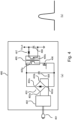
- Part (a) of Figure 4 is a circuit diagram showing a circuit configure of an example of a switching power source of a capacitor input type in which a smoothing capacitor for smoothing an input DC voltage at a rear stage of the diode bridge which rectifies the full wave AC voltage which is input from the AC power source.
- a switching power source 400 which is shown in part (a) of Figure 4 is a flyback converter in which winding directions of a primary winding 405a and a secondary winding 405b of a transformer 405 are opposite directions.
- an AC voltage is input to the switching power source 400 from an AC power source (not shown).
- the AC voltage which is input is input to a diode bridge 403 through a filter circuit 402.
- the diode bridge 403 which is a rectifier circuit rectifies a full wave AC voltage which is input from input terminals 403a and 403b on an input side and outputs to terminals 403c and 403d on an output side.
- a DC voltage is output from the diode bridge 403 in which the full wave AC voltage is rectified, and is smoothed to a substantially constant voltage by an electrolytic capacitor 404 and charged.
- the transformer 405 is a transformer whose primary and secondary sides are insulated, and includes the primary winding 405a and the secondary winding 405b which is wound in an opposite direction of the primary winding. Further, the primary winding 405a is connected to a positive side of the electrolytic capacitor 404 and the terminal 403c of the diode bridge 403 on an output side on one end, and is connected to a drain terminal of a field effect transistor (hereinafter referred to as a FET) 406 on the other end. Further, a source terminal of the FET 406 is connected to a negative side of the electrolytic capacitor 404 and the terminal 403 d on the output side of the diode bridge 403.
- a field effect transistor hereinafter referred to as a FET
- a gate terminal of the FET 406 is connected to a control IC (not shown), and the FET 406 is set to ON state or OFF state according to a signal which is input to the gate terminal from the control IC.
- the secondary winding 405b includes a diode 407 and an electrolytic capacitor 408 which are rectifying and smoothing means for rectifying and smoothing a voltage which is induced by the secondary winding 405b.
- One end of the secondary winding 405b is connected to an anode terminal of the diode 407, and the other end of the secondary winding 405b is connected to a negative side of the electrolytic capacitor 408.
- a cathode terminal of the diode 407 is connected to a positive side of the electrolytic capacitor 408, and the negative side of the electrolytic capacitor 408 is connected to the other end of the secondary winding 405b and is also grounded.
- the FET 406 When the FET 406 is in a conduction state (an ON state) by applying a gate voltage from a control IC (not shown) to a gate terminal of the FET 406, a current is supplied from the electrolytic capacitor 404 and an electric power (energy) is accumulated in the primary winding 405a. And when the gate voltage supply from the control IC to the gate terminal of the FET 406 is blocked and the FET406 is in a non-conduction state (an OFF state), the electric power (energy) which is accumulated in the primary winding 405a is induced in the secondary winding 405b. The induced voltage is rectified and smoothed by the diode 407 and the electrolytic capacitor 408, and the output voltage Vout is output.
- a same function is realized by being configured of a field effect transistor (FET) instead of the diode 407, and it is possible to further suppress an electric power loss.
- FET field effect transistor
- part (b) of Figure 4 shows a current waveform of an input current of the switching power source 400 which is a flyback converter in part (a) of Figure 4 .
- the input current from the diode bridge 403 flows only when the charging voltage of the electrolytic capacitor 404 is lower than the output voltage of the diode bridge 403. Therefore, as shown in part (b) of Figure 4 , a waveform of an input current from the diode bridge 403 become a very narrow shape of a conduction angle which is a phase angle in which the input current flows, a power factor in a state that the conduction angle is very narrow is very low, and an amount of a reactive current is large.
- the flyback converter is used as an example of a switching power source of a capacitor input type and is described.
- a switching power source of a capacitor input type
- an input current waveform is similar to an input current waveform which is shown in part (b) of Figure 4 .
- Part (a) and part (b) of Figure 5 show current waveforms of composite currents in which current waveforms of the switching power source 200 in Figure 2 which are shown in part (a) of Figure 3A and part (b) of Figure 3B and current waveform of the switching power source 400 of the capacitor input type in part (a) of Figure 4 which is shown in part (b) of Figure 4 are composed.
- Part (a) of Figure 5 is the current waveforms of the composite current in which an input current waveform in part (a) of Figure 3A and an input current waveform of the switching power source 400 of the capacitor input type in part (b) of Figure 4 are composed.
- a current waveform which is shown in part (a) of Figure 5 is added by (composed of) the input current waveform of the switching power source 400 of the capacitor input type which is shown in part (a) of Figure 4 in such a way that suppressed amount of waveform in which peak portions of a waveform of a sinusoidal wave shape which is shown in part (a) of Figure 3A are suppressed is supplemented.
- a shape of the waveform is similar to waveform shape of a sinusoidal waveform, and it is possible to achieve a high power factor.
- part (b) of Figure 5 is the current waveform of the composite current in which an input current waveform in part (a) of Figure 3B and an input current waveform of the switching power source 400 of the capacitor input type in part (b) of Figure 4 are composed.
- a protrusion portion is formed in a waveform of a sinusoidal waveform shape which is shown in part (a) of Figure 3B , and, furthermore, the input current waveform of the switching power source 400 of the capacitor input type which is shown in part (b) of Figure 4 is added. Therefore, the current waveform becomes nearly triangular in shape, as shown in part (b) of Figure 5 . So it is difficult to achieve a high power factor.
- the inductor 204 includes a function to adjust the charging voltage Vc of the electrolytic capacitor 207. For example, when an inductance value of the inductor 204 is reduced, an input current from the diode bridge 203 is increased. As a result, a charging amount of the electrolytic capacitor 207 is increased and the charging voltage Vc is easily increased, then it is possible to be approximated to the input current waveform which is shown in part (a) of Figure 3A . On the other hand, when the inductance value of the inductor 204 is increased, the input current from the diode bridge 203 is decreased.
- FIG 6 is a diagram illustrating a use pattern of a product which is provided with the switching power source which is described above.
- the printer 100 is provided with the low voltage power source device 108 which includes the switching power source 200 in the embodiment which is shown in Figure 2 , as described in Figure 1 .
- an electronic device 600 is an electronic device which is different from the printer 100 and is provided with the switching power source 400 of the capacitor input type which is shown in Figure 4 as a switching power source.
- the AC plug 201 of the switching power source 200 which is mounted on the printer 100 and the AC plug 401 of the switching power source 400 which is mounted on the electronic device 600 are connected to an outlet 601 which is provided with a wall.
- the switching power source 200 and the switching power source 200 are in a state that they are connected in parallel to a same AC power source (a same AC power source outlet 601).
- the current waveform which is composed of the input current to the switching power source 200 of the printer 100 and the input current to the switching power source 400 of the electronic device 600, is approximated to a shape of a sinusoidal waveform which is shown in part (a) of Figure 5 , and it is possible to improve the power factor.
- the switching power source 200 in the embodiment includes the circuit configuration which is shown in Figure 2 and the voltage of the electrolytic capacitor 207 is set higher than the output voltage Vin of the diode bridge 203.
- the current waveform of the input current Iin becomes a waveform of the sinusoidal waveform shape such that a height of the peak portion of the sinusoidal waveform is suppressed.
- the printer 100 on which the switching power source 200 is mounted and the electronic device 600 on which the switching power source 400 of the capacitor input type is mounted are connected to a common wall outlet 601
- the printer 100 and the electronic device 600 are connected the common wall outlet 601
- a same effect is also achieved in a case that same cable taps are used for example.
- the switching power source 200 which is described in Figure 2 may be designed to support a wide range of input voltages (for example, from 85V to 264V) as a universal power source.
- a following manner may be done. That is, only an input current near a maximum load at a low input voltage may be a current waveform which includes a protrusion shape as shown in part (b) of Figure 5 .
- the input current near the maximum load is a current which flows instantaneously, when the power factor during this period is dropped, it is considered that it has no trouble.
- the inductance value of the inductor 204 is set so that the voltage of the electrolytic capacitor 207 is always higher than the output voltage Vin of the diode bridge 203.
- the input voltage is a second voltage which is lower than the first voltage
- the voltage of the electrolytic capacitor 207 may not always higher than the output voltage Vin of the diode bridge 203.
- the input voltage is the second voltage, according to the external load which is connected to the switching power source 200, it may be configured that periods when the electrolytic capacitor 207 voltage is higher and lower than the output voltage Vin of the diode bridge 203 are occurred.
- the switching power source which includes the circuit configuration which is capable of low voltage output with the high power factor and which sets the charging voltage of the electrolytic capacitor so that it is always higher than the output voltage of the diode bridge and the input current waveform is made to be the shape in which the peak value of the sinusoidal waveform is suppressed. Since the switching power source in the first embodiment is configured of only a basic circuit, there is concern that a surge voltage which is occurred during switching of the switching element may become large depending on the power which is supplied to the load and the switching power source may become noisy. In a second embodiment, a switching power source, in which a circuit which suppresses a noise is added, will be described. Incidentally, the image forming apparatus in which the switching power source in the embodiment is mounted is same as the printer 100 in the first embodiment, and same devices and same members are described by using the same reference numerals and descriptions here are omitted.
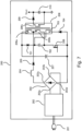
- Figure 7 is a circuit diagram showing a circuit configuration of the switching power source 200 in the embodiment.
- the circuit diagram which is shown in Figure 7 compared to the circuit diagram which is shown in Figure 2 of the first embodiment, it differs in that diodes 701 and 704, a capacitor 702, and an auxiliary winding 703 in the transformer 206 are added.
- diodes 701 and 704 compared to the circuit diagram which is shown in Figure 2 of the first embodiment, it differs in that diodes 701 and 704, a capacitor 702, and an auxiliary winding 703 in the transformer 206 are added.
- descriptions here are omitted by using same reference numerals to describe parts with same configurations as the switching power source 200 of the first embodiment which is shown in Figure 2 .
- descriptions are omitted with regard to same circuit operations as in the switching power source 200 in the first embodiment.
- one end of the capacitor 702 (a second capacitor) is connected to the other end of the primary winding 206b of the transformer 206 and the drain terminal of the FET 208, and the other end of the capacitor 702 is connected to an anode terminal of the diode 701.
- a cathode terminal of the diode 701 (a second rectifier element) is connected to a positive side of the electrolytic capacitor 207 and the other end of the primary winding 206a of the transformer 206.
- the diode 701 and the capacitor 702 are connected in series and are connected in parallel to the primary windings 206a and 206b of the transformer 206 which are connected in series.
- the anode terminal of the diode 704 (a third rectifier element) is connected to the source terminal of the FET 208, the negative side of the electrolytic capacitor 207, and the output terminal of 203d of the diode bridge 203.
- the cathode terminal of the diode 704 is connected to one end of the auxiliary winding 703 of the transformer 206.
- the other end of the auxiliary winding 703 of the transformer 206 is connected to a connection point (a second connection point) to which the other end of the capacitor 702 and the anode terminal of the diode 701 are connected.
- the diode 704 is provided for backflow prevention in order to prevent a charge of the capacitor 702 from discharging through auxiliary winding 703.
- a discharging current which flows from the capacitor 702 is divided into a current which flows through the FET 208 and a current which flows backward through the primary windings 206a and 206b.
- the current which flows backward through the primary windings 206a and 206b becomes a regenerative current to the electrolytic capacitor 207, and part of energy (a charging voltage of the capacitor 702) which is generated by a surge voltage when the FET 208 turns off is regenerated in electrolytic capacitor 207 and reused.
- the capacitor 702 in which the voltage which is charged by the surge voltage is discharged, becomes a state just before the charge current flows when the FET 208 turns off, and is reset to a state in which it is possible to accumulate the surge voltage (surge energy) again.
- the current which flows from the capacitor 702 to the FET 208 flows to the auxiliary winding 703 through the diode 704, and a current energy of the discharging current is accumulated in the auxiliary winding 703.
- the energy which is accumulated in the auxiliary winding 703 is converted as the secondary side current when the FET 208 is turned off next time, and is added to the secondary side current in which the energy which is accumulated by the current which flows in the primary windings 206a and 206b is converted.
- the switching power source 200 which is shown in Figure 7 , when the FET 208 turns on and turns off, it is configured that energy is regenerated in the electrolytic capacitor 207.
- the switching power source 200 is a highly efficient switching power source by regenerating the energy of the surge voltage while the surge voltage of the FET 208 is suppressed, since the diodes 701 and 704, the capacitor 702, and the auxiliary winding 703 are added.
- the switching power source 200 which includes a circuit configuration which is shown in Figure 7 , it is possible to make an input current waveform a current waveform as shown in part (a) of Figure 3A by setting the voltage of the electrolytic capacitor 207 to be always larger than the output voltage of the diode bridge 203.
- a product on which the switching power source 200 is mounted and an electronic device on which the switching power source of the capacitor input type are connected to a common outlet 601 ( Figure 6 )
- the switching power source which includes the circuit configuration which is capable of low voltage output with the high power factor and which sets the charging voltage of the electrolytic capacitor so that it is always higher than the output voltage of the diode bridge and the input current waveform is made to be the shape in which the peak value of the sinusoidal waveform is suppressed. And, by shaping the waveform of the input current in such a way that the peak value of the sinusoidal waveform is suppressed, it is possible to improve the power factor in the composite waveform of the input current with another electronic device 600 on which the switching power source of the capacitor input type is mounted.
- an image forming system with a configuration in which a switching power source of a capacitor input type is mounted as a main power source and a switching power source of a high power factor which is described in the first embodiment and the second embodiment is mounted as a sub-power source, will be described.
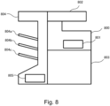
- FIG 8 is a diagram showing a configuration of an image forming system while all optional devices are mounted.
- an image forming apparatus 800 shows the smallest configuration to perform an image forming operation, and the image forming apparatus 800 by itself is able to print a sheet P based on an image data which is received according to a print request which is sent from a computer (not shown), etc.
- the image forming apparatus 800 is same as the printer 100 which is shown in Figure 1 of the first embodiment, and a description of the image forming operation will be omitted.
- An image scanner 802, an input option device 803, and an output option device 804 are mounted on the image forming apparatus 800 which is shown in Figure 8 .
- the image scanner 802 is an image reading device which reads a document which is placed on a glass table and a copy function is realized by printing the read image on a sheet P.
- the input option device 803 is possible to accommodate a large number of sheets P, and is possible to accommodate a large number of sheets P of various sizes so as to correspond to a designation of the sheet P at a time of printing.
- the output option device 804 includes a plurality of sorter bins 804a, 804b and 804c and is an optional device which includes a sorting function which sorts and outputs the sheets P which are printed.
- an output option device which includes a sorting function
- it may also be an optional processing device which processes the sheets P
- a switching power source 801 (corresponding to the low voltage power source device 108 in Figure 1 ) which is a low voltage power source device is mounted on the image forming apparatus 800, and a switching power source 805 which is a low voltage power source device is mounted on the output option device 804.
- the switching power source 801 (a first power source device) is configured as a main power source and the switching power source 805 (a second power source device) is configured as a sub-power source.
- the switching power source 801 is a switching power source of a capacitor input type
- the switching power source 805 is configured to be the switching power source of the high power factor type which is described in the first embodiment and the second embodiment and is configured so that AC voltage is supplied from a common AC power source.
- a current waveform which is composed of current waveforms of each input current of the switching power sources 801 and 805 become a shape of a substantially sinusoidal waveform as shown in Figure 3A which is described in the first embodiment, and it is possible to achieve a high power factor.
- the image forming system in the embodiment mounts all optional devices and is configured that two switching power sources of the main power source and the sub-power source are mounted as power sources.
- One of the two switching power sources is a conventional switching power source of a capacitor input type, and the other is a switching power source of a high power factor type which is described in the first embodiment and the second embodiment.
- the switching power source 805 which is mounted on the output option device 804 is a switching power source of a high power factor type and performs power supply to the output option device 804.
- the switching power source 801 of the capacitor input type which is mounted on the image forming apparatus 800 performs the power supply of the image scanner 802 and the input option device 803 in addition to the image forming apparatus.
- the switching power source of the high power factor type which supplies power to the input option device 803 is mounted on the input option device 803, and the switching power source 801 and two switching power sources of the high power factor type perform power supply.
- a power source device includes a transformer, a rectifying circuit, a series circuit, a switching element and a capacitor.
- the transformer includes first and second primary windings and a secondary winding.
- the rectifying circuit includes first and second output terminals and fully rectifies an AC voltage.
- the series circuit in which an inductor and a rectifying element are connected in series and connected between the first output terminal and a connecting point where one end of the first primary winding and one end of the second primary terminal are connected.
- the switching element is connected between the other end of the second primary winding and the second output terminal and switched between an on state and an off state.
- the capacitor is connected between the other end of the first primary winding and the second output terminal.
- An inductance of the inductor is set so that a voltage of the capacitor is higher than an output voltage of the rectifying circuit.
Landscapes
- Engineering & Computer Science (AREA)
- Power Engineering (AREA)
- Physics & Mathematics (AREA)
- General Physics & Mathematics (AREA)
- Dc-Dc Converters (AREA)
- Control Or Security For Electrophotography (AREA)
Abstract
Description
- The present invention relates to a power source device and an image forming apparatus which is provided with a power source.
- A switching power source which is used for a general electronic device often use a capacitor input type method, in which a smoothing capacitor for smoothing DC voltage is arranged at a rear stage of a diode bridge which fully rectifies an AC voltage which is input from an AC power source. A capacitor input type switching power source is characterized by a low power factor since an input current flows into a transformer when an output voltage of a diode bridge exceeds a smoothing capacitor voltage. Therefore, as a technique to increase the power factor, a switching power source is invented in which a current waveform of an input current is a shape whose peak portion is suppressed rather than a shape of a sine wave. For example, in
Japanese Patent 03288367 - However, the circuit configuration of the switching power source which is described above is based on a power factor correction circuit of a general step-up type, and is a circuit configuration which applies a transformer which outputs a relatively high voltage in which a primary side and a secondary side are not insulated. Thus, the circuit configuration is not suitable for a switching power source which uses a transformer in which the primary side and the secondary side are insulated and which outputs low voltage from several volts to several tens of volts.
- In response to such situation, an object of the present invention is to improve power factor of a switching power source in which a primary side and a secondary side are insulated from each other.
- In order to solve the problems which are described above, the present invention is provided with following configurations.
- According to an aspect of the present invention, there is provided a power source device comprising, a transformer including a first primary winding and a second primary winding, and a secondary winding, and of which a primary side and a secondary side are insulated from each other, a rectifying circuit including a first output terminal and a second output terminal, and configured to fully rectify an AC voltage, a first series circuit in which an inductor and a first rectifying element are connected in series, the first series circuit being connected between the first output terminal and a first connecting point where one end of the first primary winding and one end of the second primary terminal are connected, a switching element connected between the other end of the second primary winding and the second output terminal, and configured to be switched between an on state and an off state and a first capacitor connected between the other end of the first primary winding and the second output terminal, wherein an inductance of the inductor is set so that a voltage of the first capacitor is higher than an output voltage of the rectifying circuit, and a number of turns of the first primary winding is larger than the number of turns of the second primary winding.
- According to another aspect of the present invention, there is provided an image forming apparatus comprising, an image forming portion configured to form an image on a recording material and a power source device configured to supply power to the image forming portion, wherein the power source device including a transformer including a first primary winding and a second primary winding, and a secondary winding, and of which a primary side and a secondary side are insulated from each other, a rectifying circuit including a first output terminal and a second output terminal, and configured to fully rectify an AC voltage, a first series circuit in which an inductor and a first rectifying element are connected in series, the first series circuit being connected between the first output terminal and a first connecting point where one end of the first primary winding and one end of the second primary terminal are connected, a switching element connected between the other end of the second primary winding and the second output terminal, and configured to be switched between an on state and an off state and a first capacitor connected between the other end of the first primary winding and the second output terminal, wherein an inductance of the inductor is set so that a voltage of the first capacitor is higher than an output voltage of the rectifying circuit, and a number of turns of the first primary winding is larger than the number of turns of the second primary winding.
- According to a further aspect of the present invention, there is provided an image forming system comprising, an image forming apparatus configured to form an image on a recording material, and a processing apparatus connected to the image forming apparatus and configured to supply the recoding material to the image forming apparatus or to perform post processing to the recording material on which the image is formed by the image forming apparatus, wherein the image forming apparatus is provided with a first power source and the processing apparatus is provided with a second power source, wherein the first power source includes a first transformer of which a primary side and a secondary side are insulated from each other, a first rectifying circuit including a first output terminal and a second output terminal, and configured to fully rectify an AC voltage, a first switching element connected between one end of a primary winding of the first transformer and the second output terminal, and configured to be switched between an on state and an off state, and a first capacitor connected between the first output terminal and the second output terminal, wherein the second power source includes a second transformer including a first primary winding and a second primary winding and a secondary winding, and of which a primary side and a secondary side are insulated from each other, a second rectifying circuit including a third output terminal and a fourth output terminal, and configured to fully rectify an AC voltage, a first series circuit in which an inductor and a first rectifying element are connected in series, the first series circuit being connected between the third output terminal and a first connecting point where one end of the first primary winding and one end of the second primary terminal are connected, a second switching element connected between one end of the second primary winding and the fourth output terminal, and configured to be switched between an on state and an off state, and a second capacitor connected between the first primary winding and the second output terminal, wherein an inductance of the inductor is set so that a voltage of the second capacitor is higher than an output voltage of the second rectifying circuit.
- Further features of the present invention will become apparent from the following description of exemplary embodiments with reference to the attached drawings.
-
-
Figure 1 is a schematic sectional view illustrating a configuration of an image forming apparatus according to a first embodiment and a second embodiment. -
Figure 2 is a circuit diagram of a switching power source according to the first embodiment. - Part (a) and part (b) of
Figure 3A are graphs showing a current waveform and a voltage waveform according to the first embodiment. - Part (a) and part (b) of
Figure 3B are graphs showing a current waveform and a voltage waveform according to the first embodiment. - Part (a) and part (b) of
Figure 4 are a circuit diagram of a switching power source of a capacitor input type and a diagram illustrating a current waveform according to from the first through the third embodiments. - Part (a) and part (b) of
Figure 5 are drawings comparing input current waveforms according to the first embodiment. -
Figure 6 is a drawing illustrating a usage pattern of an electronic device according to the first embodiment. -
Figure 7 is a circuit diagram of the switching power source according to the second embodiment. -
Figure 8 is a schematic diagram of a configuration of an image forming apparatus according to the third embodiment. - In the following, embodiments of the present invention will be specifically described with reference to Figures.
- In the first embodiment, a case that a power source device according to the present invention is applied to an image forming apparatus will be described with reference to
Figures 1 through 6 .Figure 1 is a sectional view showing a schematic configure of a laser beam printer as an example of an image forming apparatus. A laser beam printer 100 (hereinafter referred to as a "printer 100") is provided with aphotosensitive drum 101 on which an electrostatic latent image is formed, acharging portion 102 which uniformly charges thephotosensitive drum 101, and a developingportion 103 which develops the electrostatic latent image which is formed on thephotosensitive drum 101 and form a toner image. Further, theprinter 100 is provided with anexposure device 110 which emits a laser light onto thephotosensitive drum 101 and form the electrostatic latent image on a surface of thephotosensitive drum 101. In theprinter 100, the toner image which is formed on thephotosensitive drum 101 is transferred to a sheet P as a recording material which is fed from acassette 104 by aroller 111, etc. with atransfer portion 105. The sheet P onto which the toner image is transferred is conveyed to afixing device 106, the toner image is fixed on the sheet P in thefixing device 106, the sheet P on which the toner image is fixed is discharged to atray 107. Thephotosensitive drum 101, thecharging portion 102, the developingportion 103, and thetransfer portion 105 are an image forming portion. Further, theprinter 100 is provided with a low voltagepower source device 108 which is a power source device, and the low voltagepower source device 108 supplies power to a driving portion such as a motor and a control portion (not shown) which controls an image forming operation by the image forming portion and conveying operation of the sheet P. -
Figure 2 is a circuit diagram showing a circuit configuration of aswitching power source 200 in the embodiment, in which theprinter 100 inFigure 1 is provided as the low voltagepower source device 108. InFigure 2 , when anAC plug 201 is connected to an outlet, AC voltage is input from a commercial AC power source (not shown) to theswitching power source 200. The input AC voltage is input to adiode bridge 203 via afilter circuit 202. Thediode bridge 203, which is a rectifier circuit, includesterminals terminals 203c (a first output terminal) and 203d (a second output terminal) on an output side. Thediode bridge 203 fully rectifies the AC voltage which is input from theterminals terminals switching power source 200 is supplied, is substantially constant and an output voltage Vout is almost stable, a charging voltage Vc, which is charged to anelectrolytic capacitor 207 which is a smoothing means, is almost constant, although the charging voltage Vc includes some ripple voltage depending on a capacity of the electrolytic capacitor. Incidentally, since theswitching power source 200 includes a power factor correction circuit, theelectrolytic capacitor 207 is configured on a downstream side of a primary winding of atransformer 206. - In
Figure 2 , theterminal 203c on the output side of thediode bridge 203 is connected to one end of aninductor 204. The other end of theinductor 204 is connected to an anode terminal of a diode 205 (a first rectifier element), and a cathode terminal of thediode 205 is connected to aprimary winding 206a (a first primary winding) and aprimary winding 206b (a second primary winding) of thetransformer 206. In this way, theinductor 204 and thediode 205 are connected in series and configures a series circuit. - The
transformer 206 is an isolation transformer for converting energy of a primary side to a secondary side and includes theprimary windings secondary winding 206c. In thetransformer 206, a polarity of theprimary windings secondary winding 206c. Theprimary winding 206a of thetransformer 206 and theprimary winding 206b are connected in series. One end of theprimary winding 206a is connected to a positive side of the electrolytic capacitor 207 (a first capacitor), and the other end of theprimary winding 206a is connected to one end of theprimary winding 206b and a cathode terminal of thediode 205. The other end of theprimary winding 206b is connected to a drain terminal of a field effect transistor (hereinafter referred to as FET) which is a switching element. On the other hand, a source terminal of the FET 208 is connected to a negative side of theelectrolytic capacitor 207 and theterminal 203 d on an output side of thediode bridge 203. That is, the FET 208 is connected to theprimary winding 206b of thetransformer 206 in series. Further, a gate terminal of the FET 208 is connected to a control IC (not shown), and the FET 208 is set to ON state or OFF state according to a signal which is input to the gate terminal from the control IC. With the connection configuration which is described above, theelectrolytic capacitor 207 is connected in parallel to the primary winding 206a andprimary winding 206b of thetransformer 206 which are connected in series. - Further, one end of the
secondary winding 206c of thetransformer 206 is connected to an anode terminal of adiode 209, and the cathode terminal of thediode 209 is connected to a positive side of anelectrolytic capacitor 210. The positive side of theelectrolytic capacitor 210 is connected to the cathode terminal of thediode 209 and the negative side of theelectrolytic capacitor 210 is connected to the other end of thesecondary winding 206c. A charge voltage of theelectrolytic capacitor 210 is output to the external load which is connected to theswitching power source 200 as the output voltage Vout of theswitching power source 200. - When the
FET 208 becomes a conductive state by an application of a gate voltage from the control IC (not shown) to a gate terminal of theFET 208, a charge voltage of theelectrolytic capacitor 207 is divided by theprimary winding 206a and theprimary winding 206b of thetransformer 206. When an output voltage of thediode bridge 203 is higher than the divided voltage, an input current to thetransformer 206 flows to theinductor 204 and thediode 205. - Here, by increasing the number of turns of the
primary winding 206a over the number of turns of theprimary winding 206b, a voltage value which is divided by theprimary winding 206a and theprimary winding 206b is decreased, and an input current flows from an output voltage of thediode bridge 203 which is a lower voltage. Further, while the voltage value which is divided by theprimary windings diode bridge 203 varies sinusoidally in terms of time, the waveform of the input current also varies substantially sinusoidally. Thus, theswitching power source 200 is possible to obtain a power source characteristic with a high power factor. - On the other hand, during a period when the gate voltage is not supplied from the control IC (not shown) to the gate terminal of the
FET 208, power (energy) which is stored in the primary side of thetransformer 206 is transmitted to the secondary side. An operation of the switchingpower source 200 is similar to an operation of a flyback power source, as power is supplied to the secondary side of thetransformer 206 when theFET 208 is turned off. And it is possible to set the output voltage Vout arbitrarily according to a turn ratio of the primary winding and the secondary winding of thetransformer 206, and output from a few volts. -
Figure 3A is a diagram illustrating waveforms of an input current Iin and output voltage Vin in a state that a power factor is high, in a case that an input current to theprimary windings transformer 206 is defined as Iin and an output voltage of the terminal 203c of thediode bridge 203. A waveform diagram shown in part (a) ofFigure 3A shows a current waveform of the input current Iin in which a vertical axis indicates a current value and a horizontal axis indicates a time t, while a waveform diagram shown in part (b) ofFigure 3A shows a voltage waveform of the output voltage Vin in which a vertical axis indicates a voltage value and a horizontal axis indicates a time t. Incidentally, t1 through t6 indicate timings. In part (b) ofFigure 3A , a voltage Vc is a voltage waveform which indicates a voltage of theelectrolytic capacitor 207, and a dashed line indicates a voltage in which the voltage Vc of theelectrolytic capacitor 207 is divided by a turn ratio of the primary winding 206a and the primary winding 206b. Incidentally, the voltage which is shown by the dashed line is also a voltage at a connection point (a primary connection point) between the primary winding 206a and the primary winding 206b. - As shown in
Figure 3A , at a time (time t1 (t3, t5, ...)) when the voltage of theelectrolytic capacitor 207 is divided by the primary winding 206a and the primary winding 206b and the output voltage Vin of thediode bridge 203 exceeds the divided voltage (a divided voltage value), the input current Iin flows. The input current Iin flows until a time (time t2 (t4, t6, ...)) when the output voltage Vin becomes less than the divided voltage value. Paradoxically, until the output voltage Vin reaches the divided voltage value (for example, from time t2 to time t3), the input current Iin is configured not to flow (Iin = 0). In this way, at the time when the output voltage Vin of thediode bridge 203 exceeds the voltage of the charging voltage of theelectrolytic capacitor 207 which is divided by the primary winding 206a and the primary winding 206b, the input current Iin starts to flow, however, the input current Iin does not flow for a predetermined period of time. - Therefore, in a case that a frequency of a pulse signal which is input to the gate terminal of the FET208 and switches the
FET 208 to an ON state or an OFF state is set to a fixed frequency, a following pulse signal control is performed in order to keep the output voltage Vout of the switchingpower source 200 constant. That is, when the output voltage Vin from thediode bridge 203 is low, a width of the pulse signal which is input to the gate terminal (a time during the ON state) is widened (lengthened) and the time during the ON state of the FET208 is extended. On the other hand, when the output voltage Vin from thediode bridge 203 is high, a width of the pulse signal which is input to the gate terminal (a time during the ON state) is narrowed (shortened) and the time during the ON state of the FET208 is shortened. Therefore, the shape of the current waveform of the input current Iin is a waveform shape such that a height of a peak portion of a sinusoidal wave which includes a period when no current flows at all (a period when the input current Iin=0) is suppressed, as shown in part (a) ofFigure 3A . Incidentally, during the period when no input current Iin does not flow at all, a power supply to a load is performed by flowing a current from theelectrolytic capacitor 207 to the primary windings of thetransformer 206. Further, an important condition for the current shape of the input current Iin to become a waveform shape which is shown in part (a) ofFigure 3A is that the voltage Vc of theelectrolytic capacitor 207 is always higher than the output voltage Vin of thediode bridge 203 as shown in part (b) ofFigure 3A . - On the other hand,
Figure 3B is a diagram illustrating the current waveform of the input current Iin and the voltage waveform of the output voltage Vin in a case that the charging voltage Vc of theelectrolytic capacitor 207 is instantaneously lower than the output voltage Vin of thediode bridge 203. A waveform diagram which is shown in part (a) ofFigure 3B shows a current waveform of the input current Iin in which a vertical axis indicates a current value and a horizontal axis indicates a time t, while a waveform diagram which is shown in part (b) ofFigure 3B shows a voltage waveform of an output voltage Vin in which a vertical axis indicates a voltage value and a horizontal axis indicates a time t. Incidentally, t11 through t22 indicate timings. - The waveform diagram which is shown in
Figure 3B differs from the waveform diagram shown inFigure 3A , in that the voltage around the peak of the output voltage Vin of thediode bridge 203 is higher than the charging voltage Vc of theelectrolytic capacitor 207 inFigure 3B . When the output voltage Vin is higher than the charging voltage Vc of the electrolytic capacitor 207 (during periods from t12 through t13, t16 through t17 and t20 through t21), the input current Iin instantaneously becomes a large current. As a result, as shown in part (a) ofFigure 3B , a waveform shape of the input current Iin is such that a protrusion portion is formed around a peak value, in contrast to the current waveform which is shown in part (a) ofFigure 3A . In the embodiment, to prevent from forming protrusion portions in an input current waveform, the charging voltage Vc of theelectrolytic capacitor 207 is set to be always higher than the output voltage Vin of thediode bridge 203. Thus, it is possible for the current waveform of the input current Iin to be the waveform shape such that the peak portion of the sinusoidal wave shape which includes the period when no current flows at all is suppressed. - Part (a) of
Figure 4 is a circuit diagram showing a circuit configure of an example of a switching power source of a capacitor input type in which a smoothing capacitor for smoothing an input DC voltage at a rear stage of the diode bridge which rectifies the full wave AC voltage which is input from the AC power source. A switchingpower source 400 which is shown in part (a) ofFigure 4 is a flyback converter in which winding directions of a primary winding 405a and a secondary winding 405b of atransformer 405 are opposite directions. - In part (a) of
Figure 4 , when anAC plug 401 is connected to an outlet, an AC voltage is input to the switchingpower source 400 from an AC power source (not shown). The AC voltage which is input is input to adiode bridge 403 through afilter circuit 402. Thediode bridge 403 which is a rectifier circuit rectifies a full wave AC voltage which is input frominput terminals terminals diode bridge 403 in which the full wave AC voltage is rectified, and is smoothed to a substantially constant voltage by anelectrolytic capacitor 404 and charged. - The
transformer 405 is a transformer whose primary and secondary sides are insulated, and includes the primary winding 405a and the secondary winding 405b which is wound in an opposite direction of the primary winding. Further, the primary winding 405a is connected to a positive side of theelectrolytic capacitor 404 and the terminal 403c of thediode bridge 403 on an output side on one end, and is connected to a drain terminal of a field effect transistor (hereinafter referred to as a FET) 406 on the other end. Further, a source terminal of theFET 406 is connected to a negative side of theelectrolytic capacitor 404 and the terminal 403 d on the output side of thediode bridge 403. Further, a gate terminal of theFET 406 is connected to a control IC (not shown), and theFET 406 is set to ON state or OFF state according to a signal which is input to the gate terminal from the control IC. Further, the secondary winding 405b includes adiode 407 and anelectrolytic capacitor 408 which are rectifying and smoothing means for rectifying and smoothing a voltage which is induced by the secondary winding 405b. One end of the secondary winding 405b is connected to an anode terminal of thediode 407, and the other end of the secondary winding 405b is connected to a negative side of theelectrolytic capacitor 408. Further, a cathode terminal of thediode 407 is connected to a positive side of theelectrolytic capacitor 408, and the negative side of theelectrolytic capacitor 408 is connected to the other end of the secondary winding 405b and is also grounded. - When the
FET 406 is in a conduction state (an ON state) by applying a gate voltage from a control IC (not shown) to a gate terminal of theFET 406, a current is supplied from theelectrolytic capacitor 404 and an electric power (energy) is accumulated in the primary winding 405a. And when the gate voltage supply from the control IC to the gate terminal of theFET 406 is blocked and the FET406 is in a non-conduction state (an OFF state), the electric power (energy) which is accumulated in the primary winding 405a is induced in the secondary winding 405b. The induced voltage is rectified and smoothed by thediode 407 and theelectrolytic capacitor 408, and the output voltage Vout is output. Incidentally, a same function is realized by being configured of a field effect transistor (FET) instead of thediode 407, and it is possible to further suppress an electric power loss. - Further, part (b) of
Figure 4 shows a current waveform of an input current of the switchingpower source 400 which is a flyback converter in part (a) ofFigure 4 . In a circuit diagram of part (a) ofFigure 4 , the input current from thediode bridge 403 flows only when the charging voltage of theelectrolytic capacitor 404 is lower than the output voltage of thediode bridge 403. Therefore, as shown in part (b) ofFigure 4 , a waveform of an input current from thediode bridge 403 become a very narrow shape of a conduction angle which is a phase angle in which the input current flows, a power factor in a state that the conduction angle is very narrow is very low, and an amount of a reactive current is large. Incidentally, here, the flyback converter is used as an example of a switching power source of a capacitor input type and is described. For example, even though other type of a power source such as a forward converter and a LLC power source in which winding directions of the primary winding and the secondary winding are same, an input current waveform is similar to an input current waveform which is shown in part (b) ofFigure 4 . - Part (a) and part (b) of
Figure 5 show current waveforms of composite currents in which current waveforms of the switchingpower source 200 inFigure 2 which are shown in part (a) ofFigure 3A and part (b) ofFigure 3B and current waveform of the switchingpower source 400 of the capacitor input type in part (a) ofFigure 4 which is shown in part (b) ofFigure 4 are composed. Part (a) ofFigure 5 is the current waveforms of the composite current in which an input current waveform in part (a) ofFigure 3A and an input current waveform of the switchingpower source 400 of the capacitor input type in part (b) ofFigure 4 are composed. A current waveform which is shown in part (a) ofFigure 5 is added by (composed of) the input current waveform of the switchingpower source 400 of the capacitor input type which is shown in part (a) ofFigure 4 in such a way that suppressed amount of waveform in which peak portions of a waveform of a sinusoidal wave shape which is shown in part (a) ofFigure 3A are suppressed is supplemented. Thus, a shape of the waveform is similar to waveform shape of a sinusoidal waveform, and it is possible to achieve a high power factor. - On the other hand, part (b) of
Figure 5 is the current waveform of the composite current in which an input current waveform in part (a) ofFigure 3B and an input current waveform of the switchingpower source 400 of the capacitor input type in part (b) ofFigure 4 are composed. In the current waveform which is shown in part (b) ofFigure 5 , a protrusion portion is formed in a waveform of a sinusoidal waveform shape which is shown in part (a) ofFigure 3B , and, furthermore, the input current waveform of the switchingpower source 400 of the capacitor input type which is shown in part (b) ofFigure 4 is added. Therefore, the current waveform becomes nearly triangular in shape, as shown in part (b) ofFigure 5 . So it is difficult to achieve a high power factor. - In a circuit configuration of the switching
power source 200 which is shown inFigure 2 , theinductor 204 includes a function to adjust the charging voltage Vc of theelectrolytic capacitor 207. For example, when an inductance value of theinductor 204 is reduced, an input current from thediode bridge 203 is increased. As a result, a charging amount of theelectrolytic capacitor 207 is increased and the charging voltage Vc is easily increased, then it is possible to be approximated to the input current waveform which is shown in part (a) ofFigure 3A . On the other hand, when the inductance value of theinductor 204 is increased, the input current from thediode bridge 203 is decreased. As a result, a discharging amount of theelectrolytic capacitor 207 is increased and the charging voltage Vc is easily decreased, then it is easily to become the input current waveform which is shown in part (a) ofFigure 3B . In this way, the inductance value of theinductor 204 is greatly affected by the input voltage range conditions of the switchingpower source 200, and also greatly affects a withstand voltage of theelectrolytic capacitor 207. Therefore, it is necessary to consider and adjust power source specifications of the switchingpower source 200 and ratings of components which are used. -
Figure 6 is a diagram illustrating a use pattern of a product which is provided with the switching power source which is described above. InFigure 6 , theprinter 100 is provided with the low voltagepower source device 108 which includes the switchingpower source 200 in the embodiment which is shown inFigure 2 , as described inFigure 1 . On the other hand, anelectronic device 600 is an electronic device which is different from theprinter 100 and is provided with the switchingpower source 400 of the capacitor input type which is shown inFigure 4 as a switching power source. And the AC plug 201 of the switchingpower source 200 which is mounted on theprinter 100 and the AC plug 401 of the switchingpower source 400 which is mounted on theelectronic device 600 are connected to anoutlet 601 which is provided with a wall. As shown inFigure 6 , the switchingpower source 200 and the switchingpower source 200 are in a state that they are connected in parallel to a same AC power source (a same AC power source outlet 601). At this time, as described above, the current waveform, which is composed of the input current to the switchingpower source 200 of theprinter 100 and the input current to the switchingpower source 400 of theelectronic device 600, is approximated to a shape of a sinusoidal waveform which is shown in part (a) ofFigure 5 , and it is possible to improve the power factor. - As described above, the switching
power source 200 in the embodiment includes the circuit configuration which is shown inFigure 2 and the voltage of theelectrolytic capacitor 207 is set higher than the output voltage Vin of thediode bridge 203. As a result, the current waveform of the input current Iin becomes a waveform of the sinusoidal waveform shape such that a height of the peak portion of the sinusoidal waveform is suppressed. As a result, in a case that theprinter 100 on which theswitching power source 200 is mounted and theelectronic device 600 on which theswitching power source 400 of the capacitor input type is mounted are connected to acommon wall outlet 601, it is possible to increase a power factor of a composed current waveform of both of the devices. Incidentally, in the embodiment, it is described by using an example that theprinter 100 and theelectronic device 600 are connected thecommon wall outlet 601, however, a same effect is also achieved in a case that same cable taps are used for example. - Further, the switching
power source 200 which is described inFigure 2 may be designed to support a wide range of input voltages (for example, from 85V to 264V) as a universal power source. At this time, in a case that it is difficult to make entire input voltage range and load current range input current waveforms without any protrusion portions as shown in part (a) ofFigure 3A , a following manner may be done. That is, only an input current near a maximum load at a low input voltage may be a current waveform which includes a protrusion shape as shown in part (b) ofFigure 5 . In this case, since the input current near the maximum load is a current which flows instantaneously, when the power factor during this period is dropped, it is considered that it has no trouble. That is, in a case that a voltage which is input to thediode bridge 203 is a first voltage, the inductance value of theinductor 204 is set so that the voltage of theelectrolytic capacitor 207 is always higher than the output voltage Vin of thediode bridge 203. At this time, in a case that the input voltage is a second voltage which is lower than the first voltage, the voltage of theelectrolytic capacitor 207 may not always higher than the output voltage Vin of thediode bridge 203. In a case the input voltage is the second voltage, according to the external load which is connected to the switchingpower source 200, it may be configured that periods when theelectrolytic capacitor 207 voltage is higher and lower than the output voltage Vin of thediode bridge 203 are occurred. - As described above, according to the embodiment, it is possible to improve the power factor of the switching power source in which the primary side and the secondary side are insulated.
- In the first embodiment, the switching power source, which includes the circuit configuration which is capable of low voltage output with the high power factor and which sets the charging voltage of the electrolytic capacitor so that it is always higher than the output voltage of the diode bridge and the input current waveform is made to be the shape in which the peak value of the sinusoidal waveform is suppressed, is described. Since the switching power source in the first embodiment is configured of only a basic circuit, there is concern that a surge voltage which is occurred during switching of the switching element may become large depending on the power which is supplied to the load and the switching power source may become noisy. In a second embodiment, a switching power source, in which a circuit which suppresses a noise is added, will be described. Incidentally, the image forming apparatus in which the switching power source in the embodiment is mounted is same as the
printer 100 in the first embodiment, and same devices and same members are described by using the same reference numerals and descriptions here are omitted. -
Figure 7 is a circuit diagram showing a circuit configuration of the switchingpower source 200 in the embodiment. In the circuit diagram which is shown inFigure 7 , compared to the circuit diagram which is shown inFigure 2 of the first embodiment, it differs in thatdiodes capacitor 702, and an auxiliary winding 703 in thetransformer 206 are added. Incidentally, in the switchingpower source 200 in the embodiment, descriptions here are omitted by using same reference numerals to describe parts with same configurations as the switchingpower source 200 of the first embodiment which is shown inFigure 2 . Further, in the switchingpower source 200 in the embodiment, descriptions are omitted with regard to same circuit operations as in the switchingpower source 200 in the first embodiment. - In
Figure 7 , one end of the capacitor 702 (a second capacitor) is connected to the other end of the primary winding 206b of thetransformer 206 and the drain terminal of theFET 208, and the other end of thecapacitor 702 is connected to an anode terminal of thediode 701. Further, a cathode terminal of the diode 701 (a second rectifier element) is connected to a positive side of theelectrolytic capacitor 207 and the other end of the primary winding 206a of thetransformer 206. Thediode 701 and thecapacitor 702 are connected in series and are connected in parallel to theprimary windings transformer 206 which are connected in series. - The anode terminal of the diode 704 (a third rectifier element) is connected to the source terminal of the
FET 208, the negative side of theelectrolytic capacitor 207, and the output terminal of 203d of thediode bridge 203. The cathode terminal of thediode 704 is connected to one end of the auxiliary winding 703 of thetransformer 206. The other end of the auxiliary winding 703 of thetransformer 206 is connected to a connection point (a second connection point) to which the other end of thecapacitor 702 and the anode terminal of thediode 701 are connected. Incidentally, thediode 704 is provided for backflow prevention in order to prevent a charge of thecapacitor 702 from discharging through auxiliary winding 703. - In
Figure 7 , when theFET 208 is turned off, through the primary winding 206b oftransformer 206, a current which flows between the drain terminal and the source terminal of theFET 208 switches to a charging current which charges a capacitance between the drain terminal and the source terminal. As a result, a voltage between the drain terminal and the source terminal of theFET 208 gradually increases due to the charging current. And when the voltage between the drain terminal and the source terminal of theFET 208 exceeds a charging voltage of theelectrolytic capacitor 207, a current from the primary winding 206b flows to theelectrolytic capacitor 207 through thecapacitor 702 and thediode 701. At this time, the voltage between the drain terminal and the source terminal of theFET 208 is suppressed to a predetermined voltage value. - On the other hand, when the
FET 208 is turned on, a discharging current which flows from thecapacitor 702 is divided into a current which flows through theFET 208 and a current which flows backward through theprimary windings primary windings electrolytic capacitor 207, and part of energy (a charging voltage of the capacitor 702) which is generated by a surge voltage when theFET 208 turns off is regenerated inelectrolytic capacitor 207 and reused. And by flowing the discharging current, thecapacitor 702, in which the voltage which is charged by the surge voltage is discharged, becomes a state just before the charge current flows when theFET 208 turns off, and is reset to a state in which it is possible to accumulate the surge voltage (surge energy) again. - On the other hand, the current which flows from the
capacitor 702 to theFET 208 flows to the auxiliary winding 703 through thediode 704, and a current energy of the discharging current is accumulated in the auxiliary winding 703. And the energy which is accumulated in the auxiliary winding 703 is converted as the secondary side current when theFET 208 is turned off next time, and is added to the secondary side current in which the energy which is accumulated by the current which flows in theprimary windings power source 200 which is shown inFigure 7 , when theFET 208 turns on and turns off, it is configured that energy is regenerated in theelectrolytic capacitor 207. Thus, the switchingpower source 200 is a highly efficient switching power source by regenerating the energy of the surge voltage while the surge voltage of theFET 208 is suppressed, since thediodes capacitor 702, and the auxiliary winding 703 are added. - Further, in the switching
power source 200 which includes a circuit configuration which is shown inFigure 7 , it is possible to make an input current waveform a current waveform as shown in part (a) ofFigure 3A by setting the voltage of theelectrolytic capacitor 207 to be always larger than the output voltage of thediode bridge 203. In a case that a product on which theswitching power source 200 is mounted and an electronic device on which the switching power source of the capacitor input type are connected to a common outlet 601 (Figure 6 ), it is possible to approximate a composite current waveform of both devices to a sinusoidal waveform shape and to make the power factor higher. - As described above, according to the embodiment, it is possible to improve the power factor of the switching power source in which the primary side and the secondary side are insulated.
- In the first embodiment and the second embodiment, the switching power source, which includes the circuit configuration which is capable of low voltage output with the high power factor and which sets the charging voltage of the electrolytic capacitor so that it is always higher than the output voltage of the diode bridge and the input current waveform is made to be the shape in which the peak value of the sinusoidal waveform is suppressed, is described. And, by shaping the waveform of the input current in such a way that the peak value of the sinusoidal waveform is suppressed, it is possible to improve the power factor in the composite waveform of the input current with another
electronic device 600 on which the switching power source of the capacitor input type is mounted. In a third embodiment, an image forming system with a configuration, in which a switching power source of a capacitor input type is mounted as a main power source and a switching power source of a high power factor which is described in the first embodiment and the second embodiment is mounted as a sub-power source, will be described. -
Figure 8 is a diagram showing a configuration of an image forming system while all optional devices are mounted. InFigure 8 , animage forming apparatus 800 shows the smallest configuration to perform an image forming operation, and theimage forming apparatus 800 by itself is able to print a sheet P based on an image data which is received according to a print request which is sent from a computer (not shown), etc. Incidentally, theimage forming apparatus 800 is same as theprinter 100 which is shown inFigure 1 of the first embodiment, and a description of the image forming operation will be omitted. - An
image scanner 802, aninput option device 803, and anoutput option device 804 are mounted on theimage forming apparatus 800 which is shown inFigure 8 . Theimage scanner 802 is an image reading device which reads a document which is placed on a glass table and a copy function is realized by printing the read image on a sheet P. Theinput option device 803 is possible to accommodate a large number of sheets P, and is possible to accommodate a large number of sheets P of various sizes so as to correspond to a designation of the sheet P at a time of printing. Theoutput option device 804 includes a plurality ofsorter bins - Further, in the image forming system which is shown in
Figure 8 , a switching power source 801 (corresponding to the low voltagepower source device 108 inFigure 1 ) which is a low voltage power source device is mounted on theimage forming apparatus 800, and a switchingpower source 805 which is a low voltage power source device is mounted on theoutput option device 804. And in the image forming system ofFigure 8 , the switching power source 801 (a first power source device) is configured as a main power source and the switching power source 805 (a second power source device) is configured as a sub-power source. For example, when a singleswitching power source 801 is configured to be able to supply power to all optional devices, in a case of theimage forming apparatus 800 alone in which no optional devices are mounted at all, power supply capability from the switchingpower source 801 become in an excessive state. As a result, costs of the switchingpower source 801 become no longer optimal. Therefore, in a case that a plurality of optional devices are mounted as shown inFigure 8 , it is more likely to reduce overall costs when it is configured with two switchingpower sources power source 801 is a switching power source of a capacitor input type, and the switchingpower source 805 is configured to be the switching power source of the high power factor type which is described in the first embodiment and the second embodiment and is configured so that AC voltage is supplied from a common AC power source. Thus, a current waveform which is composed of current waveforms of each input current of the switchingpower sources Figure 3A which is described in the first embodiment, and it is possible to achieve a high power factor. - As described above, the image forming system in the embodiment mounts all optional devices and is configured that two switching power sources of the main power source and the sub-power source are mounted as power sources. One of the two switching power sources is a conventional switching power source of a capacitor input type, and the other is a switching power source of a high power factor type which is described in the first embodiment and the second embodiment. By a configuration of the power source device, it is possible to approximate the composite waveform of the input current of each switching power source to a sinusoidal wave and to improve the power factor. Incidentally, in the embodiment, the switching
power source 805 which is mounted on theoutput option device 804 is a switching power source of a high power factor type and performs power supply to theoutput option device 804. On the other hand, it is configured that the switchingpower source 801 of the capacitor input type which is mounted on theimage forming apparatus 800 performs the power supply of theimage scanner 802 and theinput option device 803 in addition to the image forming apparatus. Incidentally, it is possible to achieve a similar effect even when it is configured that, for example, the switching power source of the high power factor type which supplies power to theinput option device 803 is mounted on theinput option device 803, and the switchingpower source 801 and two switching power sources of the high power factor type perform power supply. - As described above, according to the embodiment, it is possible to improve the power factor of the switching power source in which the primary side and the secondary side are insulated.
- While the present invention has been described with reference to exemplary embodiments, it is to be understood that the invention is not limited to the disclosed exemplary embodiments. The scope of the following claims is to be accorded the broadest interpretation so as to encompass all such modifications and equivalent structures and functions.
- A power source device includes a transformer, a rectifying circuit, a series circuit, a switching element and a capacitor. The transformer includes first and second primary windings and a secondary winding. The rectifying circuit includes first and second output terminals and fully rectifies an AC voltage. The series circuit in which an inductor and a rectifying element are connected in series and connected between the first output terminal and a connecting point where one end of the first primary winding and one end of the second primary terminal are connected. The switching element is connected between the other end of the second primary winding and the second output terminal and switched between an on state and an off state. The capacitor is connected between the other end of the first primary winding and the second output terminal. An inductance of the inductor is set so that a voltage of the capacitor is higher than an output voltage of the rectifying circuit.
Claims (15)
- A power source device comprising:a transformer including a first primary winding and a second primary winding, and a secondary winding, and of which a primary side and a secondary side are insulated from each other;a rectifying circuit including a first output terminal and a second output terminal, and configured to fully rectify an AC voltage;a first series circuit in which an inductor and a first rectifying element are connected in series, the first series circuit being connected between the first output terminal and a first connecting point where one end of the first primary winding and one end of the second primary terminal are connected;a switching element connected between the other end of the second primary winding and the second output terminal, and configured to be switched between an on state and an off state; anda first capacitor connected between the other end of the first primary winding and the second output terminal,wherein an inductance of the inductor is set so that a voltage of the first capacitor is higher than an output voltage of the rectifying circuit, and a number of turns of the first primary winding is larger than the number of turns of the second primary winding.
- A power source according to Claim 1, wherein the larger the number of turns of the first primary winding than the number of turns of the second primary winding becomes, the lower the voltage of the first capacitor becomes when a current flows through the first series circuit.
- A power source according to Claim 1, wherein the lower the inductance of the inductor becomes, the larger the current flowing through the first series circuit becomes.
- A power source according to Claim 3, wherein the first rectifying element is a first diode,the inductor is connected between the first output terminal and an anode terminal of the first diode, anda cathode terminal of the first diode is connected to the first connecting point.
- A power source according to Claim 4, wherein the transformer includes an auxiliary winding, and further comprisinga second series circuit in which a second capacitor and a second rectifying element are connected in series, the second series circuit being connected between the other end of the first primary winding and the other end of the second primary winding, anda third series circuit in which a third rectifying element the auxiliary winding are connected in series, the third series circuit being connected between the other end of the switching element and a second connecting point where the second capacitor and the second rectifying element are connected;
- A power source according to Claim 5, wherein the second rectifying element is a second diode,one end of the second capacitor is connected to the other end of the second primary winding and one end of the switching element, and the other end is connected to an anode terminal of the second diode, anda cathode terminal of the second diode is connected to the other end of the first primary winding and the one end of the first capacitor.
- A power source according to Claim 6, wherein the third rectifying element is a third diode,An anode terminal of the third diode is connected to the other end of the switching element and a cathode terminal is connected to one end of the auxiliary winding, andthe other end of the auxiliary winding is connected to the second connecting point.
- A power source according to Claim 7, wherein when the switching element is turned off, a current flowing through the second primary winding flows into the second series circuit, and a surge voltage is suppressed by the second capacitor being charged.
- A power source according to Claim 8, wherein when the switching element is turned on, a current from the second capacitor flows through the auxiliary winding of the third series circuit via the switching element.
- A power source according to Claim 9, wherein the switching element is a field effect transistor, and
one end of the switching element is a drain terminal of the field effect transistor, and the other end of the switching element is a source terminal of the field effect transistor, - A power source according to Claim 1, wherein in a case which a voltage input to the rectifying circuit is a first voltage, a voltage of the first capacitor always becomes higher than an output voltage of the rectifying circuit, and
wherein in a case which the voltage input to the rectifying circuit is a second voltage lower than the first voltage, the inductance of the inductor is set so as to generate a period where the voltage of the first capacitor is higher than the output voltage of the rectifying circuit, and a period where the voltage of the first capacitor is lower in accordance with an external load connected to the power source device. - An image forming apparatus comprising:an image forming portion configured to form a image on a recording material; anda power source device configured to supply power to the image forming portion,wherein the power source device including:a transformer including a first primary winding and a second primary winding, and a secondary winding, and of which a primary side and a secondary side are insulated from each other;a rectifying circuit including a first output terminal and a second output terminal, and configured to fully rectify an AC voltage;a first series circuit in which an inductor and a first rectifying element are connected in series, the first series circuit being connected between the first output terminal and a first connecting point where one end of the first primary winding and one end of the second primary terminal are connected;a switching element connected between the other end of the second primary winding and the second output terminal, and configured to be switched between an on state and an off state; anda first capacitor connected between the other end of the first primary winding and the second output terminal,wherein an inductance of the inductor is set so that a voltage of the first capacitor is higher than an output voltage of the rectifying circuit, and a number of turns of the first primary winding is larger than the number of turns of the second primary winding.
- An image forming apparatus according to Claim 12, wherein the transformer includes an auxiliary winding, and
the power source device further includes:a second series circuit in which a second capacitor and a second rectifying element are connected in series, the second series circuit being connected between the other end of the first primary winding and the other end of the second primary winding, anda third series circuit in which a third rectifying element the auxiliary winding are connected in series, the third series circuit being connected between the other end of the switching element and a second connecting point where the second capacitor and the second rectifying element are connected; - A power source according to Claim 12, wherein in a case which a voltage input to the rectifying circuit is a first voltage, a voltage of the first capacitor always becomes higher than an output voltage of the rectifying circuit, and
wherein in a case which the voltage input to the rectifying circuit is a second voltage lower than the first voltage, the inductance of the inductor is set so as to generate a period where the voltage of the first capacitor is higher than the output voltage of the rectifying circuit, and a period where the voltage of the first capacitor is lower in accordance with an external load connected to the power source device. - An image forming system comprising:an image forming apparatus configured to form a image on a recording material; anda processing apparatus connected to the image forming apparatus and configured to supply the recoding material to the image forming apparatus or to perform post processing to the recording material on which the image is formed by the image forming apparatus,wherein the image forming apparatus is provided with a first power source and the processing apparatus is provided with a second power source,wherein the first power source includes:a first transformer of which a primary side and a secondary side are insulated from each other;a first rectifying circuit including a first output terminal and a second output terminal, and configured to fully rectify an AC voltage;a first switching element connected between one end of a primary winding of the first transformer and the second output terminal, and configured to be switched between an on state and an off state; anda first capacitor connected between the first output terminal and the second output terminal,wherein the second power source includes:a second transformer including a first primary winding and a second primary winding and a secondary winding, and of which a primary side and a secondary side are insulated from each other;a second rectifying circuit including a third output terminal and a fourth output terminal, and configured to fully rectify an AC voltage;a first series circuit in which an inductor and a first rectifying element are connected in series, the first series circuit being connected between the third output terminal and a first connecting point where one end of the first primary winding and one end of the second primary terminal are connected;a second switching element connected between one end of the second primary winding and the fourth output terminal, and configured to be switched between an on state and an off state; anda second capacitor connected between the first primary winding and the second output terminal,wherein an inductance of the inductor is set so that a voltage of the second capacitor is higher than an output voltage of the second rectifying circuit.
Applications Claiming Priority (1)
| Application Number | Priority Date | Filing Date | Title |
|---|---|---|---|
| JP2021179726A JP7767113B2 (en) | 2021-11-02 | 2021-11-02 | Power supply device and image forming apparatus |
Publications (1)
| Publication Number | Publication Date |
|---|---|
| EP4175149A1 true EP4175149A1 (en) | 2023-05-03 |
Family
ID=83899669
Family Applications (1)
| Application Number | Title | Priority Date | Filing Date |
|---|---|---|---|
| EP22202389.7A Pending EP4175149A1 (en) | 2021-11-02 | 2022-10-19 | Power source device and image forming apparatus |
Country Status (4)
| Country | Link |
|---|---|
| US (1) | US12176818B2 (en) |
| EP (1) | EP4175149A1 (en) |
| JP (1) | JP7767113B2 (en) |
| CN (1) | CN116073674A (en) |
Families Citing this family (2)
| Publication number | Priority date | Publication date | Assignee | Title |
|---|---|---|---|---|
| JP7676212B2 (en) * | 2021-04-30 | 2025-05-14 | キヤノン株式会社 | Power supply device and image forming apparatus |
| JP2023158552A (en) | 2022-04-18 | 2023-10-30 | キヤノン株式会社 | Switching power supplies and image forming devices |
Citations (4)
| Publication number | Priority date | Publication date | Assignee | Title |
|---|---|---|---|---|
| JP3288367B2 (en) | 1999-06-28 | 2002-06-04 | 鹿児島県 | Power factor improvement circuit |
| US20210124300A1 (en) * | 2019-10-28 | 2021-04-29 | Canon Kabushiki Kaisha | Power supply apparatus and image forming apparatus |
| JP2021072768A (en) * | 2019-10-28 | 2021-05-06 | キヤノン株式会社 | Power supply device and image forming apparatus |
| JP2021132424A (en) * | 2020-02-18 | 2021-09-09 | キヤノン株式会社 | Power supply and image forming equipment |
Family Cites Families (55)
| Publication number | Priority date | Publication date | Assignee | Title |
|---|---|---|---|---|
| US4675796A (en) * | 1985-05-17 | 1987-06-23 | Veeco Instruments, Inc. | High switching frequency converter auxiliary magnetic winding and snubber circuit |
| JP3242643B2 (en) | 1990-04-05 | 2001-12-25 | 株式会社日立製作所 | Digital signal overlay recording method |
| KR100219314B1 (en) * | 1992-09-25 | 1999-09-01 | 무라따 미치히로 | Resonant power circuit |
| US5379206A (en) * | 1992-12-02 | 1995-01-03 | Argus Technologies, Ltd. | Low loss snubber circuit with active recovery switch |
| DE19610762A1 (en) * | 1996-03-19 | 1997-09-25 | Thomson Brandt Gmbh | Switching power supply with reduced harmonic load on the network |
| JP3514603B2 (en) * | 1997-03-13 | 2004-03-31 | オリジン電気株式会社 | High power factor high intensity discharge lamp lighting device and driving method thereof |
| US6038146A (en) * | 1997-06-13 | 2000-03-14 | Computer Products, Incorporated | High power factors, single stage harmonics correction converter |
| US6005780A (en) * | 1997-08-29 | 1999-12-21 | Hua; Guichao | Single-stage AC/DC conversion with PFC-tapped transformers |
| DE19855615A1 (en) * | 1997-12-03 | 1999-06-10 | Fuji Electric Co Ltd | Switched network supply device |
| US5883795A (en) * | 1998-04-28 | 1999-03-16 | Lucent Technologies Inc. | Clamp circuit for a power converter and method of operation thereof |
| EP0977346A1 (en) * | 1998-07-31 | 2000-02-02 | C.E.+ T | DC/DC converter circuit |
| JP3274431B2 (en) * | 1999-07-07 | 2002-04-15 | 長野日本無線株式会社 | Switching power supply |
| JP2001095247A (en) * | 1999-09-21 | 2001-04-06 | Sony Corp | Switching power supply circuit |
| US6115271A (en) * | 1999-10-04 | 2000-09-05 | Mo; Chan Ho Simon | Switching power converters with improved lossless snubber networks |
| US6473318B1 (en) * | 2000-11-20 | 2002-10-29 | Koninklijke Philips Electronics N.V. | Leakage energy recovering system and method for flyback converter |
| US6314002B1 (en) * | 2000-11-20 | 2001-11-06 | Philips Electronics North America Corporation | Voltage clamping system and method for a DC/DC power converter |
| JP3374917B2 (en) * | 2001-02-16 | 2003-02-10 | サンケン電気株式会社 | Switching power supply |
| JP3496717B2 (en) * | 2001-04-18 | 2004-02-16 | サンケン電気株式会社 | Switching power supply |
| JP3475943B2 (en) * | 2001-06-29 | 2003-12-10 | サンケン電気株式会社 | Switching power supply |
| JP3528921B2 (en) * | 2001-08-29 | 2004-05-24 | サンケン電気株式会社 | Switching power supply |
| JP3528920B2 (en) * | 2001-08-29 | 2004-05-24 | サンケン電気株式会社 | Switching power supply |
| JP3707436B2 (en) * | 2002-01-25 | 2005-10-19 | 株式会社村田製作所 | Switching power supply |
| JP3627708B2 (en) * | 2002-01-25 | 2005-03-09 | 株式会社村田製作所 | Switching power supply |
| JP4269588B2 (en) * | 2002-07-15 | 2009-05-27 | サンケン電気株式会社 | Switching power supply |
| JP3901088B2 (en) * | 2002-12-26 | 2007-04-04 | ソニー株式会社 | Power supply circuit and electronic equipment |
| JP4280976B2 (en) | 2003-04-10 | 2009-06-17 | 横河電機株式会社 | Switching power supply |
| JP3994942B2 (en) | 2003-07-24 | 2007-10-24 | ソニー株式会社 | Power supply circuit and electronic equipment |
| JP3861871B2 (en) * | 2003-11-26 | 2006-12-27 | サンケン電気株式会社 | Switching power supply |
| KR100681689B1 (en) * | 2004-02-03 | 2007-02-09 | 가부시키가이샤 무라타 세이사쿠쇼 | Switching power supply |
| KR101017017B1 (en) * | 2006-01-10 | 2011-02-23 | 삼성전자주식회사 | DC-DC Converters |
| JP4868260B2 (en) * | 2009-03-31 | 2012-02-01 | ブラザー工業株式会社 | Image forming apparatus and charging voltage generation method |
| CN102104337B (en) * | 2009-12-21 | 2017-03-01 | 佳能株式会社 | Power supply and image processing system |
| JP5526857B2 (en) * | 2010-02-24 | 2014-06-18 | ミツミ電機株式会社 | Semiconductor integrated circuit for power control and isolated DC power supply |
| JP5843433B2 (en) | 2010-09-30 | 2016-01-13 | キヤノン株式会社 | Power supply device and image forming apparatus |
| JP5885399B2 (en) * | 2011-05-24 | 2016-03-15 | キヤノン株式会社 | Switching power supply |
| JP5911242B2 (en) * | 2011-09-09 | 2016-04-27 | キヤノン株式会社 | Power supply device and image forming apparatus |
| JP5950635B2 (en) * | 2012-03-09 | 2016-07-13 | キヤノン株式会社 | Power supply device and image forming apparatus |
| JP6075827B2 (en) * | 2012-06-08 | 2017-02-08 | キヤノン株式会社 | Switching power supply device and image forming apparatus |
| JP6075008B2 (en) * | 2012-10-31 | 2017-02-08 | サンケン電気株式会社 | Switching power supply |
| GB2509982B (en) * | 2013-01-22 | 2015-05-27 | Tdk Lambda Uk Ltd | Converter |
| JP2015104281A (en) | 2013-11-27 | 2015-06-04 | キヤノン株式会社 | Power supply device and image forming apparatus |
| JP6300515B2 (en) | 2013-12-24 | 2018-03-28 | キヤノン株式会社 | Power supply device and image forming apparatus |
| WO2015135168A1 (en) * | 2014-03-13 | 2015-09-17 | 深圳普得技术有限公司 | Led driving circuit compatible with silicon-controlled dimmer |
| US9960664B2 (en) * | 2014-12-07 | 2018-05-01 | Alpha And Omega Semiconductor Incorporated | Voltage converter |
| JP6669387B2 (en) | 2015-12-16 | 2020-03-18 | キヤノン株式会社 | Power supply device and image forming apparatus |
| JP6859113B2 (en) * | 2017-01-20 | 2021-04-14 | キヤノン株式会社 | Power supply device and image forming device |
| JP6886107B2 (en) * | 2017-04-07 | 2021-06-16 | 富士通株式会社 | Power circuit |
| JP6843696B2 (en) * | 2017-04-28 | 2021-03-17 | キヤノン株式会社 | Power supply device and image forming device |
| JP2019047621A (en) * | 2017-09-01 | 2019-03-22 | ミツミ電機株式会社 | Semiconductor device for power supply control, power supply device, and discharge method of x capacitor |
| JP7114364B2 (en) * | 2018-06-22 | 2022-08-08 | キヤノン株式会社 | Power supply and image forming apparatus |
| JP7175699B2 (en) * | 2018-10-04 | 2022-11-21 | キヤノン株式会社 | Power supply and image forming apparatus |
| TWI732581B (en) * | 2020-06-03 | 2021-07-01 | 亞源科技股份有限公司 | Conversion device with oscillation reduction control and method of operation of oscillation reduction control the same |
| CN212231090U (en) * | 2020-06-28 | 2020-12-25 | 湖北拓实瑞丰科教设备股份有限公司 | Surge suppression circuit for discharging overvoltage spike |
| JP7676212B2 (en) * | 2021-04-30 | 2025-05-14 | キヤノン株式会社 | Power supply device and image forming apparatus |
| JP7682691B2 (en) * | 2021-05-12 | 2025-05-26 | キヤノン株式会社 | Power supply device and image forming apparatus |
-
2021
- 2021-11-02 JP JP2021179726A patent/JP7767113B2/en active Active
-
2022
- 2022-10-19 EP EP22202389.7A patent/EP4175149A1/en active Pending
- 2022-10-24 US US17/971,747 patent/US12176818B2/en active Active
- 2022-11-02 CN CN202211359826.8A patent/CN116073674A/en active Pending
Patent Citations (4)
| Publication number | Priority date | Publication date | Assignee | Title |
|---|---|---|---|---|
| JP3288367B2 (en) | 1999-06-28 | 2002-06-04 | 鹿児島県 | Power factor improvement circuit |
| US20210124300A1 (en) * | 2019-10-28 | 2021-04-29 | Canon Kabushiki Kaisha | Power supply apparatus and image forming apparatus |
| JP2021072768A (en) * | 2019-10-28 | 2021-05-06 | キヤノン株式会社 | Power supply device and image forming apparatus |
| JP2021132424A (en) * | 2020-02-18 | 2021-09-09 | キヤノン株式会社 | Power supply and image forming equipment |
Also Published As
| Publication number | Publication date |
|---|---|
| US20230135362A1 (en) | 2023-05-04 |
| CN116073674A (en) | 2023-05-05 |
| JP7767113B2 (en) | 2025-11-11 |
| US12176818B2 (en) | 2024-12-24 |
| JP2023068535A (en) | 2023-05-17 |
Similar Documents
| Publication | Publication Date | Title |
|---|---|---|
| US10547244B2 (en) | Power supply apparatus and image forming apparatus | |
| EP4175149A1 (en) | Power source device and image forming apparatus | |
| US10536085B2 (en) | Power supply apparatus and image forming apparatus | |
| EP4089922A1 (en) | Power supply device and image forming apparatus | |
| US12132405B2 (en) | Power source apparatus and image forming apparatus | |
| JP7040884B2 (en) | Power supply, image forming device and control method | |
| US11314191B2 (en) | Power supply apparatus and image forming apparatus | |
| JP7830225B2 (en) | Power supply unit and image forming apparatus | |
| JP6444090B2 (en) | Rectification smoothing circuit, power supply device and image forming apparatus | |
| US9052676B2 (en) | High-voltage power source | |
| EP2003510A1 (en) | Power supply device and image forming apparatus having the same | |
| US10263525B2 (en) | Power supply device and image forming apparatus | |
| US7907864B2 (en) | High voltage power controlling apparatus of image forming apparatus including multiple DC power supplies | |
| JP7574039B2 (en) | Image forming device | |
| US7187565B2 (en) | High voltage power supply | |
| JP2021132424A (en) | Power supply and image forming equipment | |
| JP2010115091A (en) | Power supply apparatus and image forming apparatus | |
| US12267019B2 (en) | Power supply apparatus capable of switching output resistance | |
| JP2019037073A (en) | Power supply device and image forming apparatus | |
| JP2023066894A (en) | Power supply and image forming apparatus | |
| JP2026019494A (en) | Power supply device and image forming apparatus | |
| JP2021182806A (en) | Power supply, power system and image forming equipment | |
| JPH11136943A (en) | Switching power source | |
| JPH08205519A (en) | Switching regulator | |
| JP2012029357A (en) | Power supply device and image forming device |
Legal Events
| Date | Code | Title | Description |
|---|---|---|---|
| PUAI | Public reference made under article 153(3) epc to a published international application that has entered the european phase |
Free format text: ORIGINAL CODE: 0009012 |
|
| STAA | Information on the status of an ep patent application or granted ep patent |
Free format text: STATUS: THE APPLICATION HAS BEEN PUBLISHED |
|
| AK | Designated contracting states |
Kind code of ref document: A1 Designated state(s): AL AT BE BG CH CY CZ DE DK EE ES FI FR GB GR HR HU IE IS IT LI LT LU LV MC ME MK MT NL NO PL PT RO RS SE SI SK SM TR |
|
| STAA | Information on the status of an ep patent application or granted ep patent |
Free format text: STATUS: REQUEST FOR EXAMINATION WAS MADE |
|
| 17P | Request for examination filed |
Effective date: 20231103 |
|
| RBV | Designated contracting states (corrected) |
Designated state(s): AL AT BE BG CH CY CZ DE DK EE ES FI FR GB GR HR HU IE IS IT LI LT LU LV MC ME MK MT NL NO PL PT RO RS SE SI SK SM TR |
|
| STAA | Information on the status of an ep patent application or granted ep patent |
Free format text: STATUS: EXAMINATION IS IN PROGRESS |
|
| 17Q | First examination report despatched |
Effective date: 20240129 |