EP4175056A1 - Phase shifter and phased array antenna device - Google Patents
Phase shifter and phased array antenna device Download PDFInfo
- Publication number
- EP4175056A1 EP4175056A1 EP20950212.9A EP20950212A EP4175056A1 EP 4175056 A1 EP4175056 A1 EP 4175056A1 EP 20950212 A EP20950212 A EP 20950212A EP 4175056 A1 EP4175056 A1 EP 4175056A1
- Authority
- EP
- European Patent Office
- Prior art keywords
- pass filter
- inductor
- capacitor
- phase
- elements
- Prior art date
- Legal status (The legal status is an assumption and is not a legal conclusion. Google has not performed a legal analysis and makes no representation as to the accuracy of the status listed.)
- Granted
Links
Images



Classifications
-
- H—ELECTRICITY
- H03—ELECTRONIC CIRCUITRY
- H03H—IMPEDANCE NETWORKS, e.g. RESONANT CIRCUITS; RESONATORS
- H03H7/00—Multiple-port networks comprising only passive electrical elements as network components
- H03H7/18—Networks for phase shifting
- H03H7/19—Two-port phase shifters providing a predetermined phase shift, e.g. "all-pass" filters
-
- H—ELECTRICITY
- H01—ELECTRIC ELEMENTS
- H01P—WAVEGUIDES; RESONATORS, LINES, OR OTHER DEVICES OF THE WAVEGUIDE TYPE
- H01P1/00—Auxiliary devices
- H01P1/18—Phase-shifters
-
- H—ELECTRICITY
- H01—ELECTRIC ELEMENTS
- H01Q—ANTENNAS, i.e. RADIO AERIALS
- H01Q3/00—Arrangements for changing or varying the orientation or the shape of the directional pattern of the waves radiated from an antenna or antenna system
- H01Q3/24—Arrangements for changing or varying the orientation or the shape of the directional pattern of the waves radiated from an antenna or antenna system varying the orientation by switching energy from one active radiating element to another, e.g. for beam switching
Definitions
- the present disclosure relates to a phase shifter and a phased array antenna device including the phase shifter.
- a phased array antenna device generally has a phase shifter mounted thereon that can change the phase of a signal.
- the phase shifter is connected to an antenna element included in the phased array antenna device.
- Non-Patent Literature 1 discloses a phase shifter in which a phase difference between a pass phase of a first path and a pass phase of a second path is the amount of phase shift.
- a circuit in which a plurality of first all-pass filters are connected in series is inserted in the first path, and a circuit in which a plurality of second all-pass filters are connected in series is inserted in the second path.
- the first all-pass filters each include two inductors and two capacitors as lumped-parameter elements.
- the second all-pass filters each include two inductors and two capacitors as lumped-parameter elements.
- Non-Patent Literature 1 Xinyi Tang, et al, "Large Bandwidth Digital Phase Shifters with All-pass, High-pass, and Low-pass Networks", IEEE Transactions on MTTS, Vo161, pp. 2325-2331 June 2013 .
- Non-Patent Literature 1 a combination of lumped-parameter elements that achieves an amount of phase shift and a matching condition is uniquely determined, and a frequency characteristic of the amount of phase shift is also uniquely determined. Hence, there is a problem that in a desired frequency band, a phase-shift error is uniquely determined and a desired amount of phase shift may not be able to be obtained.
- the present disclosure is made to solve a problem such as that described above, and an object of the present disclosure is to obtain a phase shifter that can achieve a frequency characteristic of a desired amount of phase shift in a desired frequency band.
- a phase shifter includes a first all-pass filter including a plurality of elements; a second all-pass filter including a plurality of elements; a first switching switch to provide a signal to either one of the first all-pass filter and the second all-pass filter; and a second switching switch to select the signal having passed through the first all-pass filter or the signal having passed through the second all-pass filter, wherein the first all-pass filter includes two inductors and three capacitors as the plurality of elements, and the second all-pass filter includes two inductors and three capacitors as the plurality of elements, or the first all-pass filter includes three inductors and two capacitors as the plurality of elements, and the second all-pass filter includes three inductors and two capacitors as the plurality of elements, and element values of the plurality of elements included in the first all-pass filter and element values of the plurality of elements included in the second all-pass filter are determined by impedance at which impedance matching is achieved, a frequency of the signal, and a variable.
- a frequency characteristic of the desired amount of phase shift can be achieved in a desired frequency band.
- FIG. 1 is a configuration diagram showing a phase shifter 1 according to a first embodiment.
- the phase shifter 1 includes a first all-pass filter 11, a second all-pass filter 12, a first switching switch 13, and a second switching switch 14.
- the first all-pass filter 11 includes two inductors and three capacitors as a plurality of elements.
- the first all-pass filter 11 includes a first inductor 21, a second inductor 24, a first capacitor 22, a second capacitor 23, and a third capacitor 25 as a plurality of elements.
- a pass phase ⁇ 1 of the first all-pass filter 11 is determined by an element value of each of the first inductor 21, the second inductor 24, the first capacitor 22, the second capacitor 23, and the third capacitor 25.
- the second all-pass filter 12 includes two inductors and three capacitors as a plurality of elements.
- the second all-pass filter 12 includes a third inductor 31, a fourth inductor 34, a fourth capacitor 32, a fifth capacitor 33, and a sixth capacitor 35 as a plurality of elements.
- a pass phase ⁇ 2 of the second all-pass filter 12 is determined by an element value of each of the third inductor 31, the fourth inductor 34, the fourth capacitor 32, the fifth capacitor 33, and the sixth capacitor 35.
- a connection terminal 13a of the first switching switch 13 is connected to either one of one end 20a of a first path 20 and one end 30a of a second path 30.
- the first switching switch 13 provides a signal to either one of the first all-pass filter 11 and the second all-pass filter 12.
- the first switching switch 13 when the connection terminal 13a is connected to the one end 20a of the first path 20, the first switching switch 13 provides a signal to the first all-pass filter 11.
- connection terminal 13a When the connection terminal 13a is connected to the one end 30a of the second path 30, the first switching switch 13 provides a signal to the second all-pass filter 12.
- a connection terminal 14a of the second switching switch 14 is connected to either one of the other end 20b of the first path 20 and the other end 30b of the second path 30.
- the second switching switch 14 selects a signal having passed through the first all-pass filter 11 or a signal having passed through the second all-pass filter 12.
- the second switching switch 14 selects a signal having passed through the first all-pass filter 11.
- connection terminal 13a of the first switching switch 13 When the connection terminal 13a of the first switching switch 13 is connected to the one end 20a of the first path 20 and the connection terminal 14a is connected to the other end 30b of the second path 30, the second switching switch 14 selects a signal having passed through the second all-pass filter 12.
- the first path 20 is a path that connects the first switching switch 13 to the second switching switch 14.
- the first inductor 21 is inserted in the first path 20.
- the second path 30 is a path that connects the first switching switch 13 to the second switching switch 14.
- the third inductor 31 is inserted in the second path 30.
- the one end 20a of the first path 20 or the one end 30a of the second path 30 is connected to the connection terminal 13a of the first switching switch 13.
- the other end 20b of the first path 20 or the other end 30b of the second path 30 is connected to the connection terminal 14a of the second switching switch 14.
- the first inductor 21 is inserted in the first path 20.
- the element value of the first inductor 21 is L 1r .
- One end of the first capacitor 22 is connected to one end of the first inductor 21.
- the other end of the first capacitor 22 is connected to each of the other end of the second capacitor 23 and one end of the second inductor 24.
- the element value of the first capacitor 22 is C 1r .
- One end of the second capacitor 23 is connected to the other end of the first inductor 21.
- the other end of the second capacitor 23 is connected to each of the other end of the first capacitor 22 and the one end of the second inductor 24.
- the element value of the second capacitor 23 is C 1r .
- the one end of the second inductor 24 is connected to the other end of each of the first capacitor 22 and the second capacitor 23.
- the other end of the second inductor 24 is connected to one end of the third capacitor 25.
- the element value of the second inductor 24 is L 2r .
- the one end of the third capacitor 25 is connected to the other end of the second inductor 24.
- the other end of the third capacitor 25 is grounded.
- the element value of the third capacitor 25 is C 2r .
- the third inductor 31 is inserted in the second path 30.
- the element value of the third inductor 31 is L 1p .
- One end of the fourth capacitor 32 is connected to one end of the third inductor 31.
- the other end of the fourth capacitor 32 is connected to each of the other end of the fifth capacitor 33 and one end of the fourth inductor 34.
- the element value of the fourth capacitor 32 is C 1p .
- One end of the fifth capacitor 33 is connected to the other end of the third inductor 31.
- the other end of the fifth capacitor 33 is connected to each of the other end of the fourth capacitor 32 and the one end of the fourth inductor 34.
- the element value of the fifth capacitor 33 is C 1p .
- the one end of the fourth inductor 34 is connected to the other end of each of the fourth capacitor 32 and the fifth capacitor 33.
- the other end of the fourth inductor 34 is connected to one end of the sixth capacitor 35.
- the element value of the fourth inductor 34 is L 2p .
- the one end of the sixth capacitor 35 is connected to the other end of the fourth inductor 34.
- the other end of the sixth capacitor 35 is grounded.
- the element value of the sixth capacitor 35 is C 2p .
- the first all-pass filter 11 forms a phase reference circuit and the second all-pass filter 12 forms a phase-delay circuit.
- the amount of phase shift ⁇ of the phase shifter 1 shown in FIG. 1 is determined by a phase difference between a pass phase ⁇ 1 of the first all-pass filter 11 and a pass phase ⁇ 2 of the second all-pass filter 12.
- connection terminal 13a of the first switching switch 13 When the connection terminal 13a of the first switching switch 13 is connected to the one end 20a of the first path 20, a signal is provided to the first all-pass filter 11 from, for example, a transmitter which is not shown through the first switching switch 13.
- connection terminal 14a of the second switching switch 14 When the connection terminal 14a of the second switching switch 14 is connected to the other end 20b of the first path 20, the signal having passed through the first all-pass filter 11 is outputted to, for example, an antenna element which is not shown through the second switching switch 14.
- connection terminal 13a of the first switching switch 13 When the connection terminal 13a of the first switching switch 13 is connected to the one end 30a of the second path 30, a signal is provided to the second all-pass filter 12 from, for example, the transmitter which is not shown through the first switching switch 13.
- connection terminal 14a of the second switching switch 14 When the connection terminal 14a of the second switching switch 14 is connected to the other end 30b of the second path 30, the signal having passed through the second all-pass filter 12 is outputted to, for example, the antenna element which is not shown through the second switching switch 14.
- the impedance of each of the antenna element and the transmitter is Z 0 , and the phase shifter 1 achieves both of impedance matching with the antenna element and impedance matching with the transmitter.
- the phase shifter 1 can achieve impedance matching at all frequencies.
- ⁇ 0 is the center angular frequency of a frequency band of each of the first all-pass filter 11 and the second all-pass filter 12, and ⁇ t and G are common variables for each element value.
- each of ⁇ t and G is a free variable for changing the amount of phase shift ⁇ 0 at the center angular frequency ⁇ 0 .
- each of the first all-pass filters and the second all-pass filters includes two inductors and two capacitors as a plurality of elements
- the phase shifter described in Non-Patent Literature 1 has one free variable ⁇ t for changing the amount of phase shift ⁇ 0 at the center angular frequency ⁇ 0 .By determining ⁇ t , a combination of elements is uniquely determined and the amounts of phase shift other than that at the center angular frequency ⁇ 0 are also uniquely determined, and thus, a frequency characteristic of the amount of phase shift is uniquely determined. Thus, there is little flexibility in design for widening frequency band. Hence, in a desired frequency band, a phase-shift error is uniquely determined, and thus, a desired amount of phase shift may not be able to be obtained.
- the phase shifter 1 shown in FIG. 1 has two free variables ⁇ t and G for changing the amount of phase shift ⁇ , and there is more flexibility in design for widening frequency band than in the phase shifter described in Non-Patent Literature 1.
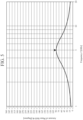
- FIG. 2 is an explanatory diagram showing simulation results of the amount of phase shift ⁇ of the phase shifter 1 shown in FIG. 1 .
- FIG. 2 Simulations of FIG. 2 are shown for the phase shifter 1 that is designed with a center frequency f 0 of 5.0 [GHz] and an amount of phase shift ⁇ 0 at the center frequency f 0 of 90 [degrees].
- the phase shifter 1 is configured in such a manner that the phase shifter 1 includes the first all-pass filter 11 including a plurality of elements; the second all-pass filter 12 including a plurality of elements; the first switching switch 13 that provides a signal to either one of the first all-pass filter 11 and the second all-pass filter 12; and the second switching switch 14 that selects the signal having passed through the first all-pass filter 11 or the signal having passed through the second all-pass filter 12, and the first all-pass filter 11 includes two inductors and three capacitors as the plurality of elements, and the second all-pass filter 12 includes two inductors and three capacitors as the plurality of elements, and element values of the plurality of elements included in the first all-pass filter 11 and element values of the plurality of elements included in the second all-pass filter 12 are determined by impedance at which impedance matching is achieved, the frequency of the signal, and a variable.
- the phase shifter 1 can achieve a frequency characteristic of the desired amount of phase shift in a
- a phase shifter 1 in which a first all-pass filter 15 includes three inductors and two capacitors as a plurality of elements and a second all-pass filter 16 includes three inductors and two capacitors as a plurality of elements.
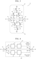
- FIG. 3 is a configuration diagram showing the phase shifter 1 according to the second embodiment.
- the same reference signs as those of FIG. 1 indicate the same or corresponding portions and thus description thereof is omitted.
- the phase shifter 1 includes the first all-pass filter 15, the second all-pass filter 16, a first switching switch 13, and a second switching switch 14.
- the first all-pass filter 15 includes three inductors and two capacitors as a plurality of elements.
- the first all-pass filter 15 includes a first inductor 42, a second inductor 43, a third inductor 45, a first capacitor 41, and a second capacitor 44 as a plurality of elements.
- a pass phase ⁇ 1 of the first all-pass filter 15 is determined by an element value of each of the first inductor 42, the second inductor 43, the third inductor 45, the first capacitor 41, and the second capacitor 44.
- the second all-pass filter 16 includes three inductors and two capacitors as a plurality of elements.
- the second all-pass filter 16 includes a fourth inductor 52, a fifth inductor 53, a sixth inductor 55, a third capacitor 51, and a fourth capacitor 54 as a plurality of elements.
- a pass phase ⁇ 2 of the second all-pass filter 16 is determined by an element value of each of the fourth inductor 52, the fifth inductor 53, the sixth inductor 55, the third capacitor 51, and the fourth capacitor 54.
- the first capacitor 41 is inserted in a first path 20.
- the element value of the first capacitor 41 is C 1r '.
- One end of the first inductor 42 is connected to one end of the first capacitor 41.
- the other end of the first inductor 42 is connected to each of the other end of the second inductor 43 and one end of the second capacitor 44.
- the element value of the first inductor 42 is L 1r '.
- One end of the second inductor 43 is connected to the other end of the first capacitor 41.
- the other end of the second inductor 43 is connected to each of the other end of the first inductor 42 and the one end of the second capacitor 44.
- the element value of the second inductor 43 is L 1r '.
- the one end of the second capacitor 44 is connected to the other end of each of the first inductor 42 and the second inductor 43.
- the other end of the second capacitor 44 is connected to one end of the third inductor 45.
- the element value of the second capacitor 44 is C 2r '.
- the one end of the third inductor 45 is connected to the other end of the second capacitor 44.
- the other end of the third inductor 45 is grounded.
- the element value of the third inductor 45 is L 2r '.
- the third capacitor 51 is inserted in a second path 30.
- the element value of the third capacitor 51 is C 1p '.
- One end of the fourth inductor 52 is connected to one end of the third capacitor 51.
- the other end of the fourth inductor 52 is connected to each of the other end of the fifth inductor 53 and one end of the fourth capacitor 54.
- the element value of the fourth inductor 52 is L 1p '.
- One end of the fifth inductor 53 is connected to the other end of the third capacitor 51.
- the other end of the fifth inductor 53 is connected to each of the other end of the fourth inductor 52 and the one end of the fourth capacitor 54.
- the element value of the fifth inductor 53 is L 1p '.
- the one end of the fourth capacitor 54 is connected to the other end of each of the fourth inductor 52 and the fifth inductor 53.
- the other end of the fourth capacitor 54 is connected to one end of the sixth inductor 55.
- the element value of the fourth capacitor 54 is C 2p '.
- the one end of the sixth inductor 55 is connected to the other end of the fourth capacitor 54.
- the other end of the sixth inductor 55 is grounded.
- the element value of the sixth inductor 55 is L 2p ' .
- the first all-pass filter 15 forms a phase reference circuit and the second all-pass filter 16 forms a phase-delay circuit.
- the amount of phase shift ⁇ of the phase shifter 1 shown in FIG. 3 is determined by a phase difference between the pass phase ⁇ 1 of the first all-pass filter 15 and the pass phase ⁇ 2 of the second all-pass filter 16.
- connection terminal 13a of the first switching switch 13 When a connection terminal 13a of the first switching switch 13 is connected to one end 20a of the first path 20, a signal is provided to the first all-pass filter 15 from, for example, a transmitter which is not shown through the first switching switch 13.
- connection terminal 14a of the second switching switch 14 When a connection terminal 14a of the second switching switch 14 is connected to the other end 20b of the first path 20, the signal having passed through the first all-pass filter 15 is outputted to, for example, an antenna element which is not shown through the second switching switch 14.
- connection terminal 13a of the first switching switch 13 When the connection terminal 13a of the first switching switch 13 is connected to one end 30a of the second path 30, a signal is provided to the second all-pass filter 16 from, for example, the transmitter which is not shown through the first switching switch 13.
- connection terminal 14a of the second switching switch 14 When the connection terminal 14a of the second switching switch 14 is connected to the other end 30b of the second path 30, the signal having passed through the second all-pass filter 16 is outputted to, for example, the antenna element which is not shown through the second switching switch 14.
- the impedance of each of the antenna element and the transmitter is Z 0 , and the phase shifter 1 achieves both of impedance matching with the antenna element and impedance matching with the transmitter.
- the phase shifter 1 can achieve impedance matching at all frequencies.
- ⁇ 0 is the center angular frequency of a frequency band of each of the first all-pass filter 15 and the second all-pass filter 16, and ⁇ t and G are common variables for each element value.
- each of ⁇ t and G is a free variable for changing the amount of phase shift ⁇ 0 at the center angular frequency ⁇ 0 .
- the phase shifter 1 is configured in such a manner that the phase shifter 1 includes the first all-pass filter 15 including a plurality of elements; the second all-pass filter 16 including a plurality of elements; the first switching switch 13 that provides a signal to either one of the first all-pass filter 15 and the second all-pass filter 16; and the second switching switch 14 that selects the signal having passed through the first all-pass filter 15 or the signal having passed through the second all-pass filter 16, and the first all-pass filter 15 includes three inductors and two capacitors as the plurality of elements, and the second all-pass filter 16 includes three inductors and two capacitors as the plurality of elements, and element values of the plurality of elements included in the first all-pass filter 15 and element values of the plurality of elements included in the second all-pass filter 16 are determined by impedance at which impedance matching is achieved, the frequency of the signal, and a variable.
- the phase shifter 1 can achieve a frequency characteristic of the desired amount of phase shift in a
- phase shifter 1 in which a plurality of first all-pass filters 11 inserted in a first path 20 are connected in series and a plurality of second all-pass filters 12 inserted in a second path 30 are connected in series.
- FIG. 4 is a configuration diagram showing the phase shifter 1 according to the third embodiment.
- the same reference signs as those of FIGS. 1 and 3 indicate the same or corresponding portions and thus description thereof is omitted.
- a phase reference circuit 61 is provided between a first switching switch 13 and a second switching switch 14, and includes a plurality of first all-pass filters 11 shown in FIG. 1 .
- the plurality of first all-pass filters 11 are connected in series with each other.
- the phase reference circuit 61 includes the plurality of first all-pass filters 11.
- the phase reference circuit 61 may include a plurality of first all-pass filters 15 shown in FIG. 3 , instead of the first all-pass filters 11 shown in FIG. 1 .
- a phase-delay circuit 62 is provided between the first switching switch 13 and the second switching switch 14, and includes a plurality of second all-pass filters 12 shown in FIG. 1 .
- the plurality of second all-pass filters 12 are connected in series with each other.
- the phase-delay circuit 62 includes the plurality of second all-pass filters 12.
- the phase-delay circuit 62 may include a plurality of second all-pass filters 16 shown in FIG. 3 , instead of the second all-pass filters 12 shown in FIG. 1 .
- a pass phase of the phase reference circuit 61 is a total sum of pass phases ⁇ 1 of the plurality of first all-pass filters 11, and a pass phase of the phase-delay circuit 62 is a total sum of pass phases ⁇ 2 of the plurality of second all-pass filters 12.
- the amount of phase shift ⁇ of the phase shifter 1 shown in FIG. 4 is determined by a phase difference between the pass phase of the phase reference circuit 61 and the pass phase of the phase-delay circuit 62.
- FIGS. 5 and 2 are explanatory diagrams showing simulation results of the amount of phase shift ⁇ obtained when the phase reference circuit 61 includes only one first all-pass filter 11 (hereinafter, referred to as “first all-pass filter 11 at the first stage") and the phase-delay circuit 62 includes only one second all-pass filter 12 (hereinafter, referred to as “second all-pass filter 12 at the first stage").
- each element value is designed in such a manner that when the center frequency f 0 is 5.0 [GHz], the amount of phase shift ⁇ 0 at the center frequency f 0 is 90 degrees, and the amount of phase shift ⁇ of the phase shifter 1 has a maximal value at the center frequency f 0 .
- each element value is designed in such a manner that when the center frequency f 0 is 5.0 [GHz], the amount of phase shift ⁇ 0 at the center frequency f 0 is 90 degrees, and the amount of phase shift ⁇ of the phase shifter 1 has a minimal value at the center frequency f 0 .
- phase reference circuit 61 includes two first all-pass filters 11, and the phase-delay circuit 62 includes two second all-pass filters 12.
- a first all-pass filter 11 that is the first one from the first switching switch 13 is a first all-pass filter 11 at the first stage
- a first all-pass filter 11 that is the second one from the first switching switch 13 is a first all-pass filter 11 at the second stage.
- a second all-pass filter 12 that is the first one from the first switching switch 13 is a second all-pass filter 12 at the first stage
- a second all-pass filter 12 that is the second one from the first switching switch 13 is a second all-pass filter 12 at the second stage.
- each element value is designed in such a manner that for the amount of phase shift ⁇ produced by the first all-pass filter 11 at the first stage and the second all-pass filter 12 at the first stage, as shown in FIG. 5 , the amount of phase shift ⁇ 0 at the center frequency f 0 is 90 degrees, and the amount of phase shift ⁇ of the phase shifter 1 has a maximal value at the center frequency f 0 .
- each element value is designed in such a manner that for the amount of phase shift ⁇ produced by the first all-pass filter 11 at the second stage and the second all-pass filter 12 at the second stage, as shown in FIG. 2 , the amount of phase shift ⁇ 0 at the center frequency f 0 is 90 degrees, and the amount of phase shift ⁇ of the phase shifter 1 has a minimal value at the center frequency f 0 .
- frequency dependence of the amount of phase shift ⁇ produced by the first all-pass filter 11 at the first stage and the second all-pass filter 12 at the first stage and frequency dependence of the amount of phase shift ⁇ produced by the first all-pass filter 11 at the second stage and the second all-pass filter 12 at the second stage compensate for each other.
- a phase-shift error of the phase shifter 1 is reduced.
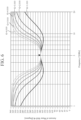
- FIG. 6 is an explanatory diagram showing simulation results of the amount of phase shift ⁇ of the phase shifter 1 shown in FIG. 4 .
- the center frequency f 0 is 5.0 [GHz] and a variable G for element values included in the first all-pass filter 11 at the second stage and the second all-pass filter 12 at the second stage is changed.
- phase reference circuit 61 includes two first all-pass filters 11 and the phase-delay circuit 62 includes two second all-pass filters 12, and the amounts of phase shift for the first stage and the second stage both achieve the amount of phase shift ⁇ 0 at the center frequency f 0 .
- the phase reference circuit 61 may include N first all-pass filters 11 and the phase-delay circuit 62 may include N second all-pass filters 12, and the center frequency f 0 and the amount of phase shift ⁇ 0 at the center frequency f 0 for each stage may vary between stages.
- each circuit may include only all-pass filters whose frequency characteristic of the amount of phase shift ⁇ at each stage has a maximal value, or may include only all-pass filters whose frequency characteristic of the amount of phase shift ⁇ at each stage has a minimal value.
- each circuit may include a combination of all-pass filters whose frequency characteristic of the amount of phase shift ⁇ at each stage has a maximal value and all-pass filters whose frequency characteristic of the amount of phase shift ⁇ at each stage has a minimal value.
- the order of cascade connection of the N first all-pass filters 11 may be any and the order of cascade connection of the N second all-pass filters 12 may be any.
- phase shifter 1 in which a phase reference circuit 61 includes a third all-pass filter 17 in addition to a first all-pass filter 11, and a phase-delay circuit 62 includes a fourth all-pass filter 18 in addition to a second all-pass filter 12.
- FIG. 7 is a configuration diagram showing the phase shifter 1 according to the fourth embodiment.
- the same reference signs as those of FIGS. 1 , 3, and 4 indicate the same or corresponding portions and thus description thereof is omitted.
- the third all-pass filter 17 is connected in series with the first all-pass filter 11.
- the third all-pass filter 17 includes two inductors and two capacitors as a plurality of elements.
- the third all-pass filter 17 includes inductors 72 and 73 and capacitors 71 and 74 as a plurality of elements.
- the capacitor 71 is inserted in a first path 20.
- One end of the inductor 72 is connected to one end of the capacitor 71.
- the other end of the inductor 72 is connected to each of the other end of the inductor 73 and one end of the capacitor 74.
- One end of the inductor 73 is connected to the other end of the capacitor 71.
- the other end of the inductor 73 is connected to each of the other end of the inductor 72 and the one end of the capacitor 74.
- the one end of the capacitor 74 is connected to each of the other end of the inductor 72 and the other end of the inductor 73.
- the other end of the capacitor 74 is grounded.
- the fourth all-pass filter 18 is connected in series with the second all-pass filter 12.
- the fourth all-pass filter 18 includes two inductors and two capacitors as a plurality of elements.
- the fourth all-pass filter 18 includes inductors 82 and 83 and capacitors 81 and 84 as a plurality of elements.
- the capacitor 81 is inserted in a second path 30.
- One end of the inductor 82 is connected to one end of the capacitor 81.
- the other end of the inductor 82 is connected to each of the other end of the inductor 83 and one end of the capacitor 84.
- One end of the inductor 83 is connected to the other end of the capacitor 81.
- the other end of the inductor 83 is connected to each of the other end of the inductor 82 and the one end of the capacitor 84.
- the one end of the capacitor 84 is connected to each of the other end of the inductor 82 and the other end of the inductor 83.
- the other end of the capacitor 84 is grounded.
- the phase reference circuit 61 includes the third all-pass filter 17 in addition to the first all-pass filter 11, and the phase-delay circuit 62 includes the fourth all-pass filter 18 in addition to the second all-pass filter 12.
- phase reference circuit 61 may include the third all-pass filter 17 in addition to a first all-pass filter 15, and the phase-delay circuit 62 may include the fourth all-pass filter 18 in addition to a second all-pass filter 16.
- phase reference circuit 61 may include the third all-pass filter 17 in addition to the first all-pass filter 11 and a first all-pass filter 15, and the phase-delay circuit 62 may include the fourth all-pass filter 18 in addition to the second all-pass filter 12 and a second all-pass filter 16.
- the third all-pass filter 17 corresponds to the first all-pass filter described in Non-Patent Literature 1.
- the fourth all-pass filter 18 corresponds to the second all-pass filter described in Non-Patent Literature 1.
- phase shifter that includes only the third all-pass filter 17 included in the phase reference circuit 61 and the fourth all-pass filter 18 included in the phase-delay circuit 62 cannot change a frequency characteristic of the amount of phase shift while impedance matching is achieved.
- phase reference circuit 61 includes the first all-pass filter 11 and the phase-delay circuit 62 includes the second all-pass filter 12, and thus, the amount of phase shift can be changed while impedance matching is achieved.
- the elements included in the third all-pass filter 17 are two inductors 72 and 73 and two capacitors 71 and 74, and the number of the elements included in the third all-pass filter 17 is smaller than the number of elements included in the first all-pass filter 11.
- the elements included in the fourth all-pass filter 18 are two inductors 82 and 83 and two capacitors 81 and 84, and the number of the elements included in the fourth all-pass filter 18 is smaller than the number of elements included in the second all-pass filter 12.
- phase shifter 1 shown in FIG. 7 can achieve a further size reduction than in the phase shifter 1 shown in FIG. 4 under conditions that the number of stages of all-pass filters included in the phase reference circuit 61 is the same and the number of stages of all-pass filters included in the phase-delay circuit 62 is the same.
- phase shifter 1 shown in FIG. 7 as long as the third all-pass filter 17 includes two inductors 72 and 73 and two capacitors 71 and 74, disposition of each of the two inductors 72 and 73 and the two capacitors 71 and 74 is not limited to that shown in FIG. 7 .
- the inductor 72 may be disposed at a location where the capacitor 71 is disposed, the inductor 73 may be disposed at a location where the capacitor 74 is disposed, the capacitor 71 may be disposed at a location where the inductor 72 is disposed, and the capacitor 74 may be disposed at a location where the inductor 73 is disposed.
- phase shifter 1 shown in FIG. 7 as long as the fourth all-pass filter 18 includes two inductors 82 and 83 and two capacitors 81 and 84, disposition of each of the two inductors 82 and 83 and the two capacitors 81 and 84 is not limited to that shown in FIG. 7 .
- the inductor 82 may be disposed at a location where the capacitor 81 is disposed, the inductor 83 may be disposed at a location where the capacitor 84 is disposed, the capacitor 81 may be disposed at a location where the inductor 82 is disposed, and the capacitor 84 may be disposed at a location where the inductor 83 is disposed.
- phased array antenna device including a phase shifter 1 according to any one of the first to fourth embodiments will be described.
- FIG. 8 is a configuration diagram showing a phased array antenna device according to a fifth embodiment.
- M is an integer greater than or equal to 2.
- the phase shifter 92-m is the phase shifter 1 according to any one of the first to fourth embodiments.
- the phase shifter 92-m shifts the phase of the transmission signal outputted from the transmitter 91-m, and outputs the phase-shifted transmission signal to an antenna element 93-m.
- the antenna element 93-m radiates a radio wave based on the transmission signal whose phase has been shifted by the phase shifter 92-m into space.
- the phased array antenna device shown in FIG. 8 radiates radio waves based on transmission signals into space. However, this is merely an example, and the phased array antenna device may receive radio waves.
- the antenna element 93-m of the phased array antenna device receives a radio wave
- the antenna element 93-m outputs a reception signal of the radio wave to the phase shifter 92-m.
- the phase shifter 92-m shifts the phase of the reception signal outputted from the antenna element 93-m, and outputs the phase-shifted reception signal to a receiver which is not shown.
- the present disclosure is suitable for a phase shifter.
- the present disclosure is suitable for a phased array antenna device including a phase shifter.
Landscapes
- Filters And Equalizers (AREA)
- Waveguide Switches, Polarizers, And Phase Shifters (AREA)
- Variable-Direction Aerials And Aerial Arrays (AREA)
Abstract
Description
- The present disclosure relates to a phase shifter and a phased array antenna device including the phase shifter.
- A phased array antenna device generally has a phase shifter mounted thereon that can change the phase of a signal. The phase shifter is connected to an antenna element included in the phased array antenna device.
- The following
Non-Patent Literature 1 discloses a phase shifter in which a phase difference between a pass phase of a first path and a pass phase of a second path is the amount of phase shift. A circuit in which a plurality of first all-pass filters are connected in series is inserted in the first path, and a circuit in which a plurality of second all-pass filters are connected in series is inserted in the second path. The first all-pass filters each include two inductors and two capacitors as lumped-parameter elements. In addition, the second all-pass filters each include two inductors and two capacitors as lumped-parameter elements. - Non-Patent Literature 1: Xinyi Tang, et al, "Large Bandwidth Digital Phase Shifters with All-pass, High-pass, and Low-pass Networks", IEEE Transactions on MTTS, Vo161, pp. 2325-2331 June 2013.
- In the phase shifter disclosed in
Non-Patent Literature 1, a combination of lumped-parameter elements that achieves an amount of phase shift and a matching condition is uniquely determined, and a frequency characteristic of the amount of phase shift is also uniquely determined. Hence, there is a problem that in a desired frequency band, a phase-shift error is uniquely determined and a desired amount of phase shift may not be able to be obtained. - The present disclosure is made to solve a problem such as that described above, and an object of the present disclosure is to obtain a phase shifter that can achieve a frequency characteristic of a desired amount of phase shift in a desired frequency band.
- A phase shifter according to the present disclosure includes a first all-pass filter including a plurality of elements; a second all-pass filter including a plurality of elements; a first switching switch to provide a signal to either one of the first all-pass filter and the second all-pass filter; and a second switching switch to select the signal having passed through the first all-pass filter or the signal having passed through the second all-pass filter, wherein the first all-pass filter includes two inductors and three capacitors as the plurality of elements, and the second all-pass filter includes two inductors and three capacitors as the plurality of elements, or the first all-pass filter includes three inductors and two capacitors as the plurality of elements, and the second all-pass filter includes three inductors and two capacitors as the plurality of elements, and element values of the plurality of elements included in the first all-pass filter and element values of the plurality of elements included in the second all-pass filter are determined by impedance at which impedance matching is achieved, a frequency of the signal, and a variable.
- According to the present disclosure, a frequency characteristic of the desired amount of phase shift can be achieved in a desired frequency band.
-
-
FIG. 1 is a configuration diagram showing aphase shifter 1 according to a first embodiment. -
FIG. 2 is an explanatory diagram showing simulation results of an amount of phase shift Φ of thephase shifter 1 shown inFIG. 1 . -
FIG. 3 is a configuration diagram showing aphase shifter 1 according to a second embodiment. -
FIG. 4 is a configuration diagram showing aphase shifter 1 according to a third embodiment. -
FIG. 5 is an explanatory diagram showing a simulation result of the amount of phase shift Φ obtained when aphase reference circuit 61 includes only one first all-pass filter 11 and a phase-delay circuit 62 includes only one second all-pass filter 12. -
FIG. 6 is an explanatory diagram showing simulation results of the amount of phase shift Φ of thephase shifter 1 shown inFIG. 4 . -
FIG. 7 is a configuration diagram showing aphase shifter 1 according to a fourth embodiment. -
FIG. 8 is a configuration diagram showing a phased array antenna device according to a fifth embodiment. - To describe the present disclosure in more detail, embodiments for carrying out the present disclosure will be described below with reference to the accompanying drawings.
-
FIG. 1 is a configuration diagram showing aphase shifter 1 according to a first embodiment. - The
phase shifter 1 includes a first all-pass filter 11, a second all-pass filter 12, afirst switching switch 13, and asecond switching switch 14. - The first all-
pass filter 11 includes two inductors and three capacitors as a plurality of elements. - Namely, the first all-
pass filter 11 includes afirst inductor 21, asecond inductor 24, afirst capacitor 22, asecond capacitor 23, and athird capacitor 25 as a plurality of elements. - A pass phase Φ1 of the first all-
pass filter 11 is determined by an element value of each of thefirst inductor 21, thesecond inductor 24, thefirst capacitor 22, thesecond capacitor 23, and thethird capacitor 25. - The second all-
pass filter 12 includes two inductors and three capacitors as a plurality of elements. - Namely, the second all-
pass filter 12 includes athird inductor 31, afourth inductor 34, afourth capacitor 32, afifth capacitor 33, and asixth capacitor 35 as a plurality of elements. - A pass phase Φ2 of the second all-
pass filter 12 is determined by an element value of each of thethird inductor 31, thefourth inductor 34, thefourth capacitor 32, thefifth capacitor 33, and thesixth capacitor 35. - A
connection terminal 13a of thefirst switching switch 13 is connected to either one of oneend 20a of afirst path 20 and oneend 30a of asecond path 30. - The
first switching switch 13 provides a signal to either one of the first all-pass filter 11 and the second all-pass filter 12. - Namely, when the
connection terminal 13a is connected to the oneend 20a of thefirst path 20, thefirst switching switch 13 provides a signal to the first all-pass filter 11. - When the
connection terminal 13a is connected to the oneend 30a of thesecond path 30, thefirst switching switch 13 provides a signal to the second all-pass filter 12. - A
connection terminal 14a of thesecond switching switch 14 is connected to either one of theother end 20b of thefirst path 20 and theother end 30b of thesecond path 30. - The
second switching switch 14 selects a signal having passed through the first all-pass filter 11 or a signal having passed through the second all-pass filter 12. - Namely, when the
connection terminal 13a of thefirst switching switch 13 is connected to the oneend 20a of thefirst path 20 and theconnection terminal 14a is connected to theother end 20b of thefirst path 20, thesecond switching switch 14 selects a signal having passed through the first all-pass filter 11. - When the
connection terminal 13a of thefirst switching switch 13 is connected to the oneend 20a of thefirst path 20 and theconnection terminal 14a is connected to theother end 30b of thesecond path 30, thesecond switching switch 14 selects a signal having passed through the second all-pass filter 12. - The
first path 20 is a path that connects thefirst switching switch 13 to thesecond switching switch 14. Thefirst inductor 21 is inserted in thefirst path 20. - The
second path 30 is a path that connects thefirst switching switch 13 to thesecond switching switch 14. Thethird inductor 31 is inserted in thesecond path 30. - The one
end 20a of thefirst path 20 or the oneend 30a of thesecond path 30 is connected to theconnection terminal 13a of thefirst switching switch 13. - The
other end 20b of thefirst path 20 or theother end 30b of thesecond path 30 is connected to theconnection terminal 14a of thesecond switching switch 14. - The
first inductor 21 is inserted in thefirst path 20. - The element value of the
first inductor 21 is L1r. - One end of the
first capacitor 22 is connected to one end of thefirst inductor 21. - The other end of the
first capacitor 22 is connected to each of the other end of thesecond capacitor 23 and one end of thesecond inductor 24. - The element value of the
first capacitor 22 is C1r. - One end of the
second capacitor 23 is connected to the other end of thefirst inductor 21. - The other end of the
second capacitor 23 is connected to each of the other end of thefirst capacitor 22 and the one end of thesecond inductor 24. - The element value of the
second capacitor 23 is C1r. - The one end of the
second inductor 24 is connected to the other end of each of thefirst capacitor 22 and thesecond capacitor 23. - The other end of the
second inductor 24 is connected to one end of thethird capacitor 25. - The element value of the
second inductor 24 is L2r. - The one end of the
third capacitor 25 is connected to the other end of thesecond inductor 24. - The other end of the
third capacitor 25 is grounded. - The element value of the
third capacitor 25 is C2r. - The
third inductor 31 is inserted in thesecond path 30. - The element value of the
third inductor 31 is L1p. - One end of the
fourth capacitor 32 is connected to one end of thethird inductor 31. - The other end of the
fourth capacitor 32 is connected to each of the other end of thefifth capacitor 33 and one end of thefourth inductor 34. - The element value of the
fourth capacitor 32 is C1p. - One end of the
fifth capacitor 33 is connected to the other end of thethird inductor 31. - The other end of the
fifth capacitor 33 is connected to each of the other end of thefourth capacitor 32 and the one end of thefourth inductor 34. - The element value of the
fifth capacitor 33 is C1p. - The one end of the
fourth inductor 34 is connected to the other end of each of thefourth capacitor 32 and thefifth capacitor 33. - The other end of the
fourth inductor 34 is connected to one end of thesixth capacitor 35. - The element value of the
fourth inductor 34 is L2p. - The one end of the
sixth capacitor 35 is connected to the other end of thefourth inductor 34. - The other end of the
sixth capacitor 35 is grounded. - The element value of the
sixth capacitor 35 is C2p. - Next, operations of the
phase shifter 1 shown inFIG. 1 will be described. - The first all-
pass filter 11 forms a phase reference circuit and the second all-pass filter 12 forms a phase-delay circuit. - The amount of phase shift Φ of the
phase shifter 1 shown inFIG. 1 is determined by a phase difference between a pass phase Φ1 of the first all-pass filter 11 and a pass phase Φ2 of the second all-pass filter 12. - When the
connection terminal 13a of the first switchingswitch 13 is connected to the oneend 20a of thefirst path 20, a signal is provided to the first all-pass filter 11 from, for example, a transmitter which is not shown through the first switchingswitch 13. - When the
connection terminal 14a of thesecond switching switch 14 is connected to theother end 20b of thefirst path 20, the signal having passed through the first all-pass filter 11 is outputted to, for example, an antenna element which is not shown through thesecond switching switch 14. - When the
connection terminal 13a of the first switchingswitch 13 is connected to the oneend 30a of thesecond path 30, a signal is provided to the second all-pass filter 12 from, for example, the transmitter which is not shown through the first switchingswitch 13. - When the
connection terminal 14a of thesecond switching switch 14 is connected to theother end 30b of thesecond path 30, the signal having passed through the second all-pass filter 12 is outputted to, for example, the antenna element which is not shown through thesecond switching switch 14. - It is assumed that the impedance of each of the antenna element and the transmitter is Z0, and the
phase shifter 1 achieves both of impedance matching with the antenna element and impedance matching with the transmitter. - When the element values of the plurality of elements included in the first all-
pass filter 11 and the element values of the plurality of elements included in the second all-pass filter 12 satisfy the following equation (1), thephase shifter 1 can achieve impedance matching at all frequencies.
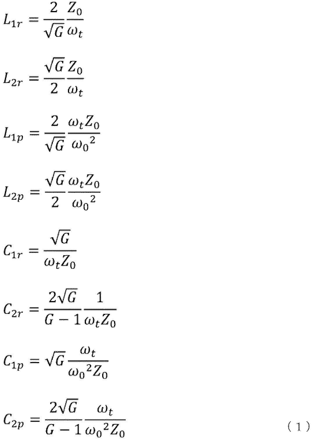
- In equation (1), ω0 is the center angular frequency of a frequency band of each of the first all-
pass filter 11 and the second all-pass filter 12, and ωt and G are common variables for each element value. - The amount of phase shift Φ of the
phase shifter 1 shown inFIG. 1 is determined by a phase difference between the pass phase Φ1 of the first all-pass filter 11 and the pass phase Φ2 of the second all-pass filter 12, and the amount of phase shift Φ0 at the center angular frequency ω0 is represented by the following equation (2):
- As shown in equation (2), each of ωt and G is a free variable for changing the amount of phase shift Φ0 at the center angular frequency ω0.
- Thus, by changing ωt or G, the amount of phase shift Φ0 at the center angular frequency ω0 can be changed while matching at impedance Z0 is achieved.
- Note that when, as in the phase shifter described in
Non-Patent Literature 1, each of the first all-pass filters and the second all-pass filters includes two inductors and two capacitors as a plurality of elements, the amount of phase shift Φ0 at the center angular frequency ω0 is represented as shown in the following equation (3):
- The phase shifter described in
Non-Patent Literature 1 has one free variable ωt for changing the amount of phase shift Φ0 at the center angular frequency ω0.By determining ωt, a combination of elements is uniquely determined and the amounts of phase shift other than that at the center angular frequency ω0 are also uniquely determined, and thus, a frequency characteristic of the amount of phase shift is uniquely determined. Thus, there is little flexibility in design for widening frequency band. Hence, in a desired frequency band, a phase-shift error is uniquely determined, and thus, a desired amount of phase shift may not be able to be obtained. - The
phase shifter 1 shown inFIG. 1 has two free variables ωt and G for changing the amount of phase shift Φ, and there is more flexibility in design for widening frequency band than in the phase shifter described inNon-Patent Literature 1. -
FIG. 2 is an explanatory diagram showing simulation results of the amount of phase shift Φ of thephase shifter 1 shown inFIG. 1 . - Simulations of
FIG. 2 are shown for thephase shifter 1 that is designed with a center frequency f0 of 5.0 [GHz] and an amount of phase shift Φ0 at the center frequency f0 of 90 [degrees]. Here, a relationship between the center frequency f0 and the center angular frequency ω0 is represented by ω0 = 2πf0. As a free variable for changing a frequency characteristic of the amount of phase shift Φ of thephase shifter 1, the variable G is changed. Namely, the amount of phase shift Φ for G = 1.010, G = 2.010, G = 3.010, G = 4.010, G = 5.010, and G = 6.010 is simulated. - As shown in
FIG. 2 , it can be seen that by changing the variable G, the frequency characteristic of the amount of phase shift Φ changes. - In the above-described first embodiment, the
phase shifter 1 is configured in such a manner that thephase shifter 1 includes the first all-pass filter 11 including a plurality of elements; the second all-pass filter 12 including a plurality of elements; the first switchingswitch 13 that provides a signal to either one of the first all-pass filter 11 and the second all-pass filter 12; and thesecond switching switch 14 that selects the signal having passed through the first all-pass filter 11 or the signal having passed through the second all-pass filter 12, and the first all-pass filter 11 includes two inductors and three capacitors as the plurality of elements, and the second all-pass filter 12 includes two inductors and three capacitors as the plurality of elements, and element values of the plurality of elements included in the first all-pass filter 11 and element values of the plurality of elements included in the second all-pass filter 12 are determined by impedance at which impedance matching is achieved, the frequency of the signal, and a variable. Thus, thephase shifter 1 can achieve a frequency characteristic of the desired amount of phase shift in a desired frequency band. - In a second embodiment, a
phase shifter 1 will be described in which a first all-pass filter 15 includes three inductors and two capacitors as a plurality of elements and a second all-pass filter 16 includes three inductors and two capacitors as a plurality of elements. -
FIG. 3 is a configuration diagram showing thephase shifter 1 according to the second embodiment. InFIG. 3 , the same reference signs as those ofFIG. 1 indicate the same or corresponding portions and thus description thereof is omitted. - The
phase shifter 1 includes the first all-pass filter 15, the second all-pass filter 16, afirst switching switch 13, and asecond switching switch 14. - The first all-
pass filter 15 includes three inductors and two capacitors as a plurality of elements. - Namely, the first all-
pass filter 15 includes afirst inductor 42, asecond inductor 43, athird inductor 45, afirst capacitor 41, and asecond capacitor 44 as a plurality of elements. - A pass phase Φ1 of the first all-
pass filter 15 is determined by an element value of each of thefirst inductor 42, thesecond inductor 43, thethird inductor 45, thefirst capacitor 41, and thesecond capacitor 44. - The second all-
pass filter 16 includes three inductors and two capacitors as a plurality of elements. - Namely, the second all-
pass filter 16 includes afourth inductor 52, afifth inductor 53, asixth inductor 55, athird capacitor 51, and afourth capacitor 54 as a plurality of elements. - A pass phase Φ2 of the second all-
pass filter 16 is determined by an element value of each of thefourth inductor 52, thefifth inductor 53, thesixth inductor 55, thethird capacitor 51, and thefourth capacitor 54. - The
first capacitor 41 is inserted in afirst path 20. - The element value of the
first capacitor 41 is C1r'. - One end of the
first inductor 42 is connected to one end of thefirst capacitor 41. - The other end of the
first inductor 42 is connected to each of the other end of thesecond inductor 43 and one end of thesecond capacitor 44. - The element value of the
first inductor 42 is L1r'. - One end of the
second inductor 43 is connected to the other end of thefirst capacitor 41. - The other end of the
second inductor 43 is connected to each of the other end of thefirst inductor 42 and the one end of thesecond capacitor 44. - The element value of the
second inductor 43 is L1r'. - The one end of the
second capacitor 44 is connected to the other end of each of thefirst inductor 42 and thesecond inductor 43. - The other end of the
second capacitor 44 is connected to one end of thethird inductor 45. - The element value of the
second capacitor 44 is C2r'. - The one end of the
third inductor 45 is connected to the other end of thesecond capacitor 44. - The other end of the
third inductor 45 is grounded. - The element value of the
third inductor 45 is L2r'. - The
third capacitor 51 is inserted in asecond path 30. - The element value of the
third capacitor 51 is C1p'. - One end of the
fourth inductor 52 is connected to one end of thethird capacitor 51. - The other end of the
fourth inductor 52 is connected to each of the other end of thefifth inductor 53 and one end of thefourth capacitor 54. - The element value of the
fourth inductor 52 is L1p'. - One end of the
fifth inductor 53 is connected to the other end of thethird capacitor 51. - The other end of the
fifth inductor 53 is connected to each of the other end of thefourth inductor 52 and the one end of thefourth capacitor 54. - The element value of the
fifth inductor 53 is L1p'. - The one end of the
fourth capacitor 54 is connected to the other end of each of thefourth inductor 52 and thefifth inductor 53. - The other end of the
fourth capacitor 54 is connected to one end of thesixth inductor 55. - The element value of the
fourth capacitor 54 is C2p'. - The one end of the
sixth inductor 55 is connected to the other end of thefourth capacitor 54. - The other end of the
sixth inductor 55 is grounded. - The element value of the
sixth inductor 55 is L2p'. - Next, operations of the
phase shifter 1 shown inFIG. 3 will be described. - The first all-
pass filter 15 forms a phase reference circuit and the second all-pass filter 16 forms a phase-delay circuit. - The amount of phase shift Φ of the
phase shifter 1 shown inFIG. 3 is determined by a phase difference between the pass phase Φ1 of the first all-pass filter 15 and the pass phase Φ2 of the second all-pass filter 16. - When a
connection terminal 13a of the first switchingswitch 13 is connected to oneend 20a of thefirst path 20, a signal is provided to the first all-pass filter 15 from, for example, a transmitter which is not shown through the first switchingswitch 13. - When a
connection terminal 14a of thesecond switching switch 14 is connected to theother end 20b of thefirst path 20, the signal having passed through the first all-pass filter 15 is outputted to, for example, an antenna element which is not shown through thesecond switching switch 14. - When the
connection terminal 13a of the first switchingswitch 13 is connected to oneend 30a of thesecond path 30, a signal is provided to the second all-pass filter 16 from, for example, the transmitter which is not shown through the first switchingswitch 13. - When the
connection terminal 14a of thesecond switching switch 14 is connected to theother end 30b of thesecond path 30, the signal having passed through the second all-pass filter 16 is outputted to, for example, the antenna element which is not shown through thesecond switching switch 14. - It is assumed that the impedance of each of the antenna element and the transmitter is Z0, and the
phase shifter 1 achieves both of impedance matching with the antenna element and impedance matching with the transmitter. - When the element values of the plurality of elements included in the first all-
pass filter 15 and the element values of the plurality of elements included in the second all-pass filter 16 satisfy the following equation (4), thephase shifter 1 can achieve impedance matching at all frequencies.

- In equation (4), ω0 is the center angular frequency of a frequency band of each of the first all-
pass filter 15 and the second all-pass filter 16, and ωt and G are common variables for each element value. - The amount of phase shift Φ of the
phase shifter 1 shown inFIG. 3 is determined by a phase difference between the pass phase Φ1 of the first all-pass filter 15 and the pass phase Φ2 of the second all-pass filter 16, and the amount of phase shift Φ0 at the center angular frequency ω0 is represented by the following equation (5):
- As shown in equation (5), each of ωt and G is a free variable for changing the amount of phase shift Φ0 at the center angular frequency ω0.
- Thus, by changing ωt or G, the amount of phase shift Φ0 at the center angular frequency ω0 can be changed while matching at impedance Z0 is achieved.
- In the above-described second embodiment, the
phase shifter 1 is configured in such a manner that thephase shifter 1 includes the first all-pass filter 15 including a plurality of elements; the second all-pass filter 16 including a plurality of elements; the first switchingswitch 13 that provides a signal to either one of the first all-pass filter 15 and the second all-pass filter 16; and thesecond switching switch 14 that selects the signal having passed through the first all-pass filter 15 or the signal having passed through the second all-pass filter 16, and the first all-pass filter 15 includes three inductors and two capacitors as the plurality of elements, and the second all-pass filter 16 includes three inductors and two capacitors as the plurality of elements, and element values of the plurality of elements included in the first all-pass filter 15 and element values of the plurality of elements included in the second all-pass filter 16 are determined by impedance at which impedance matching is achieved, the frequency of the signal, and a variable. Thus, thephase shifter 1 can achieve a frequency characteristic of the desired amount of phase shift in a desired frequency band. - In a third embodiment, a
phase shifter 1 will be described in which a plurality of first all-pass filters 11 inserted in afirst path 20 are connected in series and a plurality of second all-pass filters 12 inserted in asecond path 30 are connected in series. -
FIG. 4 is a configuration diagram showing thephase shifter 1 according to the third embodiment. InFIG. 4 , the same reference signs as those ofFIGS. 1 and3 indicate the same or corresponding portions and thus description thereof is omitted. - A
phase reference circuit 61 is provided between afirst switching switch 13 and asecond switching switch 14, and includes a plurality of first all-pass filters 11 shown inFIG. 1 . The plurality of first all-pass filters 11 are connected in series with each other. - In the
phase shifter 1 shown inFIG. 4 , thephase reference circuit 61 includes the plurality of first all-pass filters 11. However, this is merely an example, and thephase reference circuit 61 may include a plurality of first all-pass filters 15 shown inFIG. 3 , instead of the first all-pass filters 11 shown inFIG. 1 . - A phase-
delay circuit 62 is provided between the first switchingswitch 13 and thesecond switching switch 14, and includes a plurality of second all-pass filters 12 shown inFIG. 1 . The plurality of second all-pass filters 12 are connected in series with each other. - In the
phase shifter 1 shown inFIG. 4 , the phase-delay circuit 62 includes the plurality of second all-pass filters 12. However, this is merely an example, and the phase-delay circuit 62 may include a plurality of second all-pass filters 16 shown inFIG. 3 , instead of the second all-pass filters 12 shown inFIG. 1 . - A pass phase of the
phase reference circuit 61 is a total sum of pass phases Φ1 of the plurality of first all-pass filters 11, and a pass phase of the phase-delay circuit 62 is a total sum of pass phases Φ2 of the plurality of second all-pass filters 12. - The amount of phase shift Φ of the
phase shifter 1 shown inFIG. 4 is determined by a phase difference between the pass phase of thephase reference circuit 61 and the pass phase of the phase-delay circuit 62. -
FIGS. 5 and2 are explanatory diagrams showing simulation results of the amount of phase shift Φ obtained when thephase reference circuit 61 includes only one first all-pass filter 11 (hereinafter, referred to as "first all-pass filter 11 at the first stage") and the phase-delay circuit 62 includes only one second all-pass filter 12 (hereinafter, referred to as "second all-pass filter 12 at the first stage"). - In a simulation of the amount of phase shift Φ shown in
FIG. 5 , each element value is designed in such a manner that when the center frequency f0 is 5.0 [GHz], the amount of phase shift Φ0 at the center frequency f0 is 90 degrees, and the amount of phase shift Φ of thephase shifter 1 has a maximal value at the center frequency f0. - In simulations of the amount of phase shift Φ shown in
FIG. 2 , each element value is designed in such a manner that when the center frequency f0 is 5.0 [GHz], the amount of phase shift Φ0 at the center frequency f0 is 90 degrees, and the amount of phase shift Φ of thephase shifter 1 has a minimal value at the center frequency f0. - It is assumed that the
phase reference circuit 61 includes two first all-pass filters 11, and the phase-delay circuit 62 includes two second all-pass filters 12. - In this case, a first all-
pass filter 11 that is the first one from the first switchingswitch 13 is a first all-pass filter 11 at the first stage, and a first all-pass filter 11 that is the second one from the first switchingswitch 13 is a first all-pass filter 11 at the second stage. - In addition, a second all-
pass filter 12 that is the first one from the first switchingswitch 13 is a second all-pass filter 12 at the first stage, and a second all-pass filter 12 that is the second one from the first switchingswitch 13 is a second all-pass filter 12 at the second stage. - It is assumed that each element value is designed in such a manner that for the amount of phase shift Φ produced by the first all-
pass filter 11 at the first stage and the second all-pass filter 12 at the first stage, as shown inFIG. 5 , the amount of phase shift Φ0 at the center frequency f0 is 90 degrees, and the amount of phase shift Φ of thephase shifter 1 has a maximal value at the center frequency f0. - On the other hand, it is assumed that each element value is designed in such a manner that for the amount of phase shift Φ produced by the first all-
pass filter 11 at the second stage and the second all-pass filter 12 at the second stage, as shown inFIG. 2 , the amount of phase shift Φ0 at the center frequency f0 is 90 degrees, and the amount of phase shift Φ of thephase shifter 1 has a minimal value at the center frequency f0. - In a case of the above-described design, as shown in
FIG. 6 , frequency dependence of the amount of phase shift Φ produced by the first all-pass filter 11 at the first stage and the second all-pass filter 12 at the first stage and frequency dependence of the amount of phase shift Φ produced by the first all-pass filter 11 at the second stage and the second all-pass filter 12 at the second stage compensate for each other. By compensation for the frequency dependence, a phase-shift error of thephase shifter 1 is reduced. -
FIG. 6 is an explanatory diagram showing simulation results of the amount of phase shift Φ of thephase shifter 1 shown inFIG. 4 . - In simulations of the amount of phase shift Φ, the center frequency f0 is 5.0 [GHz] and a variable G for element values included in the first all-
pass filter 11 at the second stage and the second all-pass filter 12 at the second stage is changed. Namely, the amount of phase shift Φ for G = 1.010, G = 2.010, G = 3.010, G = 4.010, G = 5.010, and G = 6.010 is simulated. - As shown in
FIG. 2 , by changing the variable G for element values included in the first all-pass filter 11 at the second stage and the second all-pass filter 12 at the second stage, it can be seen that the compensation for frequency dependence of the amount of phase shift produced by each of the first all-pass filter 11 at the first stage and the second all-pass filter 12 at the first stage is performed, and a phase-shift error of thephase shifter 1 is reduced. - Here, it is assumed that the
phase reference circuit 61 includes two first all-pass filters 11 and the phase-delay circuit 62 includes two second all-pass filters 12, and the amounts of phase shift for the first stage and the second stage both achieve the amount of phase shift Φ0 at the center frequency f0. - In general, the
phase reference circuit 61 may include N first all-pass filters 11 and the phase-delay circuit 62 may include N second all-pass filters 12, and the center frequency f0 and the amount of phase shift Φ0 at the center frequency f0 for each stage may vary between stages. In addition, each circuit may include only all-pass filters whose frequency characteristic of the amount of phase shift Φ at each stage has a maximal value, or may include only all-pass filters whose frequency characteristic of the amount of phase shift Φ at each stage has a minimal value. In addition, each circuit may include a combination of all-pass filters whose frequency characteristic of the amount of phase shift Φ at each stage has a maximal value and all-pass filters whose frequency characteristic of the amount of phase shift Φ at each stage has a minimal value. The order of cascade connection of the N first all-pass filters 11 may be any and the order of cascade connection of the N second all-pass filters 12 may be any. - In a fourth embodiment, a
phase shifter 1 will be described in which aphase reference circuit 61 includes a third all-pass filter 17 in addition to a first all-pass filter 11, and a phase-delay circuit 62 includes a fourth all-pass filter 18 in addition to a second all-pass filter 12. -
FIG. 7 is a configuration diagram showing thephase shifter 1 according to the fourth embodiment. InFIG. 7 , the same reference signs as those ofFIGS. 1 ,3, and 4 indicate the same or corresponding portions and thus description thereof is omitted. - The third all-
pass filter 17 is connected in series with the first all-pass filter 11. - The third all-
pass filter 17 includes two inductors and two capacitors as a plurality of elements. - Namely, the third all-
pass filter 17 includesinductors capacitors - The
capacitor 71 is inserted in afirst path 20. - One end of the
inductor 72 is connected to one end of thecapacitor 71. - The other end of the
inductor 72 is connected to each of the other end of theinductor 73 and one end of thecapacitor 74. - One end of the
inductor 73 is connected to the other end of thecapacitor 71. - The other end of the
inductor 73 is connected to each of the other end of theinductor 72 and the one end of thecapacitor 74. - The one end of the
capacitor 74 is connected to each of the other end of theinductor 72 and the other end of theinductor 73. - The other end of the
capacitor 74 is grounded. - The fourth all-
pass filter 18 is connected in series with the second all-pass filter 12. - The fourth all-
pass filter 18 includes two inductors and two capacitors as a plurality of elements. - Namely, the fourth all-
pass filter 18 includesinductors capacitors - The
capacitor 81 is inserted in asecond path 30. - One end of the
inductor 82 is connected to one end of thecapacitor 81. - The other end of the
inductor 82 is connected to each of the other end of theinductor 83 and one end of thecapacitor 84. - One end of the
inductor 83 is connected to the other end of thecapacitor 81. - The other end of the
inductor 83 is connected to each of the other end of theinductor 82 and the one end of thecapacitor 84. - The one end of the
capacitor 84 is connected to each of the other end of theinductor 82 and the other end of theinductor 83. - The other end of the
capacitor 84 is grounded. - In the
phase shifter 1 shown inFIG. 7 , thephase reference circuit 61 includes the third all-pass filter 17 in addition to the first all-pass filter 11, and the phase-delay circuit 62 includes the fourth all-pass filter 18 in addition to the second all-pass filter 12. - However, this is merely an example, and the
phase reference circuit 61 may include the third all-pass filter 17 in addition to a first all-pass filter 15, and the phase-delay circuit 62 may include the fourth all-pass filter 18 in addition to a second all-pass filter 16. - In addition, the
phase reference circuit 61 may include the third all-pass filter 17 in addition to the first all-pass filter 11 and a first all-pass filter 15, and the phase-delay circuit 62 may include the fourth all-pass filter 18 in addition to the second all-pass filter 12 and a second all-pass filter 16. - The third all-
pass filter 17 corresponds to the first all-pass filter described inNon-Patent Literature 1. - In addition, the fourth all-
pass filter 18 corresponds to the second all-pass filter described inNon-Patent Literature 1. - Thus, a phase shifter that includes only the third all-
pass filter 17 included in thephase reference circuit 61 and the fourth all-pass filter 18 included in the phase-delay circuit 62 cannot change a frequency characteristic of the amount of phase shift while impedance matching is achieved. - However, in the
phase shifter 1 shown inFIG. 7 , thephase reference circuit 61 includes the first all-pass filter 11 and the phase-delay circuit 62 includes the second all-pass filter 12, and thus, the amount of phase shift can be changed while impedance matching is achieved. - The elements included in the third all-
pass filter 17 are twoinductors capacitors pass filter 17 is smaller than the number of elements included in the first all-pass filter 11. - In addition, the elements included in the fourth all-
pass filter 18 are twoinductors capacitors pass filter 18 is smaller than the number of elements included in the second all-pass filter 12. - Thus, the
phase shifter 1 shown inFIG. 7 can achieve a further size reduction than in thephase shifter 1 shown inFIG. 4 under conditions that the number of stages of all-pass filters included in thephase reference circuit 61 is the same and the number of stages of all-pass filters included in the phase-delay circuit 62 is the same. - In the
phase shifter 1 shown inFIG. 7 , as long as the third all-pass filter 17 includes twoinductors capacitors inductors capacitors FIG. 7 . - In
FIG. 7 , for example, theinductor 72 may be disposed at a location where thecapacitor 71 is disposed, theinductor 73 may be disposed at a location where thecapacitor 74 is disposed, thecapacitor 71 may be disposed at a location where theinductor 72 is disposed, and thecapacitor 74 may be disposed at a location where theinductor 73 is disposed. - In the
phase shifter 1 shown inFIG. 7 , as long as the fourth all-pass filter 18 includes twoinductors capacitors inductors capacitors FIG. 7 . - In
FIG. 7 , for example, theinductor 82 may be disposed at a location where thecapacitor 81 is disposed, theinductor 83 may be disposed at a location where thecapacitor 84 is disposed, thecapacitor 81 may be disposed at a location where theinductor 82 is disposed, and thecapacitor 84 may be disposed at a location where theinductor 83 is disposed. - A phased array antenna device including a
phase shifter 1 according to any one of the first to fourth embodiments will be described. -
FIG. 8 is a configuration diagram showing a phased array antenna device according to a fifth embodiment. - In
FIG. 8 , a transmitter 91-m (m = 1, ..., M) outputs a transmission signal to a phase shifter 92-m. M is an integer greater than or equal to 2. - The phase shifter 92-m is the
phase shifter 1 according to any one of the first to fourth embodiments. - The phase shifter 92-m shifts the phase of the transmission signal outputted from the transmitter 91-m, and outputs the phase-shifted transmission signal to an antenna element 93-m.
- The antenna element 93-m radiates a radio wave based on the transmission signal whose phase has been shifted by the phase shifter 92-m into space.
- The phased array antenna device shown in
FIG. 8 radiates radio waves based on transmission signals into space. However, this is merely an example, and the phased array antenna device may receive radio waves. When the antenna element 93-m of the phased array antenna device receives a radio wave, the antenna element 93-m outputs a reception signal of the radio wave to the phase shifter 92-m. - The phase shifter 92-m shifts the phase of the reception signal outputted from the antenna element 93-m, and outputs the phase-shifted reception signal to a receiver which is not shown.
- Note that in the present disclosure, a free combination of the embodiments, modifications to any component of each of the embodiments, or omissions of any component in each of the embodiments are possible.
- The present disclosure is suitable for a phase shifter.
- The present disclosure is suitable for a phased array antenna device including a phase shifter.
- 1: Phase shifter, 11: First all-pass filter, 12: Second all-pass filter, 13: First switching switch, 13a: Connection terminal, 14: Second switching switch, 14a: Connection terminal, 15: First all-pass filter, 16: Second all-pass filter, 17: Third all-pass filter, 18: Fourth all-pass filter, 20: First path, 20a: One end, 20b: Other end, 21: First inductor, 22: First capacitor, 23: Second capacitor, 24: Second inductor, 25: Third capacitor, 30: Second path, 30a: One end, 30b: Other end, 31: Third inductor, 32: Fourth capacitor, 33: Fifth capacitor, 34: Fourth inductor, 35: Sixth capacitor, 41: First capacitor, 42: First inductor, 43: Second inductor, 44: Second capacitor, 45: Third inductor, 51: Third capacitor, 52: Fourth inductor, 53: Fifth inductor, 54: Fourth capacitor, 55: Sixth inductor, 61: Phase reference circuit, 62: Phase-delay circuit, 71 and 74: Capacitor, 72 and 73: Inductor, 81 and 84: Capacitor, 82 and 83: Inductor, 91-1 to 91-M: Transmitter, 92-1 to 92-M: Phase shifter, 93-1 to 93-M: Antenna element
Claims (7)
- A phase shifter comprising:a first all-pass filter including a plurality of elements;a second all-pass filter including a plurality of elements;a first switching switch to provide a signal to either one of the first all-pass filter and the second all-pass filter; anda second switching switch to select the signal having passed through the first all-pass filter or the signal having passed through the second all-pass filter, whereinthe first all-pass filter includes two inductors and three capacitors as the plurality of elements, and the second all-pass filter includes two inductors and three capacitors as the plurality of elements, orthe first all-pass filter includes three inductors and two capacitors as the plurality of elements, and the second all-pass filter includes three inductors and two capacitors as the plurality of elements, andelement values of the plurality of elements included in the first all-pass filter and element values of the plurality of elements included in the second all-pass filter are determined by impedance at which impedance matching is achieved, a frequency of the signal, and a variable.
- The phase shifter according to claim 1, whereinthe first all-pass filter includes a first inductor, a second inductor, a first capacitor, a second capacitor, and a third capacitor as the plurality of elements,the second all-pass filter includes a third inductor, a fourth inductor, a fourth capacitor, a fifth capacitor, and a sixth capacitor as the plurality of elements,the first inductor is inserted in a first path that connects the first switching switch to the second switching switch,a first end of the first capacitor is connected to a first end of the first inductor,a first end of the second capacitor is connected to a second end of the first inductor,a first end of the second inductor is connected to a second end of each of the first capacitor and the second capacitor,a first end of the third capacitor is connected to a second end of the second inductor, and a second end of the third capacitor is grounded,the third inductor is inserted in a second path that connects the first switching switch to the second switching switch,a first end of the fourth capacitor is connected to a first end of the third inductor,a first end of the fifth capacitor is connected to a second end of the third inductor,a first end of the fourth inductor is connected to a second end of each of the fourth capacitor and the fifth capacitor, anda first end of the sixth capacitor is connected to a second end of the fourth inductor, and a second end of the sixth capacitor is grounded.
- The phase shifter according to claim 1, whereinthe first all-pass filter includes a first inductor, a second inductor, a third inductor, a first capacitor, and a second capacitor as the plurality of elements,the second all-pass filter includes a fourth inductor, a fifth inductor, a sixth inductor, a third capacitor, and a fourth capacitor as the plurality of elements,the first capacitor is inserted in a first path that connects the first switching switch to the second switching switch,a first end of the first inductor is connected to a first end of the first capacitor,a first end of the second inductor is connected to a second end of the first capacitor,a first end of the second capacitor is connected to a second end of each of the first inductor and the second inductor,a first end of the third inductor is connected to a second end of the second capacitor, and a second end of the third inductor is grounded,the third capacitor is inserted in a second path that connects the first switching switch to the second switching switch,a first end of the fourth inductor is connected to a first end of the third capacitor,a first end of the fifth inductor is connected to a second end of the third capacitor,a first end of the fourth capacitor is connected to a second end of each of the fourth inductor and the fifth inductor, anda first end of the sixth inductor is connected to a second end of the fourth capacitor, and a second end of the sixth inductor is grounded.
- The phase shifter according to claim 1, whereina plurality of first all-pass filters inserted in the first path are connected in series, anda plurality of second all-pass filters inserted in the second path are connected in series.
- The phase shifter according to claim 4, whereinthe plurality of first all-pass filters have different pass phases, andthe plurality of second all-pass filters have different pass phases.
- The phase shifter according to claim 1, comprising:a third all-pass filter including two inductors and two capacitors; anda fourth all-pass filter including two inductors and two capacitors, whereinthe third all-pass filter is connected in series with the first all-pass filter, andthe fourth all-pass filter is connected in series with the second all-pass filter.
- A phased array antenna device comprising the phase shifter according to any one of claims 1 to 6.
Applications Claiming Priority (1)
| Application Number | Priority Date | Filing Date | Title |
|---|---|---|---|
| PCT/JP2020/030932 WO2022038646A1 (en) | 2020-08-17 | 2020-08-17 | Phase shifter and phased array antenna device |
Publications (3)
| Publication Number | Publication Date |
|---|---|
| EP4175056A1 true EP4175056A1 (en) | 2023-05-03 |
| EP4175056A4 EP4175056A4 (en) | 2023-08-02 |
| EP4175056B1 EP4175056B1 (en) | 2025-01-15 |
Family
ID=80322869
Family Applications (1)
| Application Number | Title | Priority Date | Filing Date |
|---|---|---|---|
| EP20950212.9A Active EP4175056B1 (en) | 2020-08-17 | 2020-08-17 | Phase shifter and phased array antenna device |
Country Status (4)
| Country | Link |
|---|---|
| US (1) | US12323123B2 (en) |
| EP (1) | EP4175056B1 (en) |
| JP (1) | JP7150223B2 (en) |
| WO (1) | WO2022038646A1 (en) |
Families Citing this family (1)
| Publication number | Priority date | Publication date | Assignee | Title |
|---|---|---|---|---|
| CN116762275A (en) * | 2021-02-12 | 2023-09-15 | 株式会社村田制作所 | Distributors and communication devices |
Family Cites Families (10)
| Publication number | Priority date | Publication date | Assignee | Title |
|---|---|---|---|---|
| US5920241A (en) * | 1997-05-12 | 1999-07-06 | Emc Technology Llc | Passive temperature compensating LC filter |
| JP2002076810A (en) * | 2000-08-31 | 2002-03-15 | Mitsubishi Electric Corp | Phase shifter |
| US7276993B2 (en) * | 2005-05-31 | 2007-10-02 | Agile Rf, Inc. | Analog phase shifter using cascaded voltage tunable capacitor |
| JP4963241B2 (en) | 2007-02-23 | 2012-06-27 | 三菱電機株式会社 | Phase shift circuit |
| JP2011259215A (en) * | 2010-06-09 | 2011-12-22 | Toshiba Corp | Phase shifter |
| JP2013098744A (en) * | 2011-10-31 | 2013-05-20 | Sumitomo Electric Device Innovations Inc | Phase shifter and method of designing the same |
| TWI536733B (en) * | 2014-05-30 | 2016-06-01 | 國立臺灣大學 | Common mode noise suppressing device |
| JP6566441B2 (en) | 2016-01-07 | 2019-08-28 | 学校法人上智学院 | Phase shifter |
| CN107332538A (en) * | 2017-06-27 | 2017-11-07 | 中国科学院微电子研究所 | a digital phase shifter |
| JP6808096B2 (en) | 2018-06-19 | 2021-01-06 | 三菱電機株式会社 | Phaser |
-
2020
- 2020-08-17 EP EP20950212.9A patent/EP4175056B1/en active Active
- 2020-08-17 JP JP2022543816A patent/JP7150223B2/en active Active
- 2020-08-17 WO PCT/JP2020/030932 patent/WO2022038646A1/en not_active Ceased
-
2022
- 2022-12-12 US US18/079,377 patent/US12323123B2/en active Active
Also Published As
| Publication number | Publication date |
|---|---|
| US20230106157A1 (en) | 2023-04-06 |
| US12323123B2 (en) | 2025-06-03 |
| JP7150223B2 (en) | 2022-10-07 |
| EP4175056A4 (en) | 2023-08-02 |
| WO2022038646A1 (en) | 2022-02-24 |
| EP4175056B1 (en) | 2025-01-15 |
| JPWO2022038646A1 (en) | 2022-02-24 |
Similar Documents
| Publication | Publication Date | Title |
|---|---|---|
| CA2852383C (en) | Electronically tunable filter | |
| CN112260651B (en) | Broadband programmable harmonic rejection mixer | |
| US9438288B2 (en) | System providing reduced intermodulation distortion | |
| RU2495524C2 (en) | Digital conversion method and apparatus, and signal reconfiguration method | |
| CN107015206B (en) | Adaptive antenna interference detection system and method | |
| US9712313B2 (en) | Systems for multi-peak-filter-based analog self-interference cancellation | |
| KR102060029B1 (en) | Beamforming engine | |
| US12323123B2 (en) | Phase shifter comprising selectable first and second all-pass filters, where the all-pass filters include capacitors and inductors of determined values to achieve impedance matching | |
| EP3742551A1 (en) | Antenna device and wireless communication device | |
| JP4910586B2 (en) | Transmission / reception device and electronic apparatus using the same | |
| CN107144821A (en) | Efficient reception passage based on time delay Wave beam forming in wideband digital battle array radar | |
| JP7034385B2 (en) | Delay circuit and line switching type phase shifter | |
| WO2015073070A1 (en) | Methods and apparatus for signal sideband receiver/transceiver for phased array radar antenna | |
| Montaseri et al. | Analysis of HBT vector modulator phase shifters based on Gilbert cell for sub-THz regimes | |
| US12294334B2 (en) | In-phase/quadrature-phase generating device and phase shift device using the same | |
| US20230216468A1 (en) | Dual-band 360 degree phase shifter using series/parallel resonance circuit for phased array antenna system | |
| JP4864758B2 (en) | Orthogonal mixer and image rejection mixer | |
| EP3925078B1 (en) | A differential combiner circuit | |
| Kwon et al. | Wideband switchable-capacitor loaded differential phase shifter with lattice structures | |
| JP6466275B2 (en) | Phased array antenna | |
| CN216390945U (en) | Phase shift network | |
| US8600333B2 (en) | Apparatus for mixing frequency | |
| Swenson et al. | Discrete-Time Channelizers for Aeronautical Telemetry: Part I-Fixed Bandwidth | |
| JPH0515521U (en) | Image Rigidation Mixer | |
| HK1187162A (en) | Tunable filter devices and methods |
Legal Events
| Date | Code | Title | Description |
|---|---|---|---|
| STAA | Information on the status of an ep patent application or granted ep patent |
Free format text: STATUS: THE INTERNATIONAL PUBLICATION HAS BEEN MADE |
|
| PUAI | Public reference made under article 153(3) epc to a published international application that has entered the european phase |
Free format text: ORIGINAL CODE: 0009012 |
|
| STAA | Information on the status of an ep patent application or granted ep patent |
Free format text: STATUS: REQUEST FOR EXAMINATION WAS MADE |
|
| 17P | Request for examination filed |
Effective date: 20230106 |
|
| AK | Designated contracting states |
Kind code of ref document: A1 Designated state(s): AL AT BE BG CH CY CZ DE DK EE ES FI FR GB GR HR HU IE IS IT LI LT LU LV MC MK MT NL NO PL PT RO RS SE SI SK SM TR |
|
| REG | Reference to a national code |
Ref country code: DE Ref legal event code: R079 Free format text: PREVIOUS MAIN CLASS: H01P0001180000 Ipc: H03H0007190000 Ref country code: DE Ref legal event code: R079 Ref document number: 602020045011 Country of ref document: DE Free format text: PREVIOUS MAIN CLASS: H01P0001180000 Ipc: H03H0007190000 |
|
| A4 | Supplementary search report drawn up and despatched |
Effective date: 20230630 |
|
| RIC1 | Information provided on ipc code assigned before grant |
Ipc: H03H 7/19 20060101AFI20230626BHEP |
|
| DAV | Request for validation of the european patent (deleted) | ||
| DAX | Request for extension of the european patent (deleted) | ||
| STAA | Information on the status of an ep patent application or granted ep patent |
Free format text: STATUS: EXAMINATION IS IN PROGRESS |
|
| 17Q | First examination report despatched |
Effective date: 20240221 |
|
| GRAP | Despatch of communication of intention to grant a patent |
Free format text: ORIGINAL CODE: EPIDOSNIGR1 |
|
| STAA | Information on the status of an ep patent application or granted ep patent |
Free format text: STATUS: GRANT OF PATENT IS INTENDED |
|
| INTG | Intention to grant announced |
Effective date: 20240905 |
|
| GRAS | Grant fee paid |
Free format text: ORIGINAL CODE: EPIDOSNIGR3 |
|
| GRAA | (expected) grant |
Free format text: ORIGINAL CODE: 0009210 |
|
| STAA | Information on the status of an ep patent application or granted ep patent |
Free format text: STATUS: THE PATENT HAS BEEN GRANTED |
|
| AK | Designated contracting states |
Kind code of ref document: B1 Designated state(s): AL AT BE BG CH CY CZ DE DK EE ES FI FR GB GR HR HU IE IS IT LI LT LU LV MC MK MT NL NO PL PT RO RS SE SI SK SM TR |
|
| REG | Reference to a national code |
Ref country code: CH Ref legal event code: EP Ref country code: GB Ref legal event code: FG4D |
|
| REG | Reference to a national code |
Ref country code: DE Ref legal event code: R096 Ref document number: 602020045011 Country of ref document: DE |
|
| REG | Reference to a national code |
Ref country code: IE Ref legal event code: FG4D |
|
| REG | Reference to a national code |
Ref country code: NL Ref legal event code: MP Effective date: 20250115 |
|
| PG25 | Lapsed in a contracting state [announced via postgrant information from national office to epo] |
Ref country code: NL Free format text: LAPSE BECAUSE OF FAILURE TO SUBMIT A TRANSLATION OF THE DESCRIPTION OR TO PAY THE FEE WITHIN THE PRESCRIBED TIME-LIMIT Effective date: 20250115 |
|
| PG25 | Lapsed in a contracting state [announced via postgrant information from national office to epo] |
Ref country code: RS Free format text: LAPSE BECAUSE OF FAILURE TO SUBMIT A TRANSLATION OF THE DESCRIPTION OR TO PAY THE FEE WITHIN THE PRESCRIBED TIME-LIMIT Effective date: 20250415 |
|
| PG25 | Lapsed in a contracting state [announced via postgrant information from national office to epo] |
Ref country code: FI Free format text: LAPSE BECAUSE OF FAILURE TO SUBMIT A TRANSLATION OF THE DESCRIPTION OR TO PAY THE FEE WITHIN THE PRESCRIBED TIME-LIMIT Effective date: 20250115 |
|
| PG25 | Lapsed in a contracting state [announced via postgrant information from national office to epo] |
Ref country code: PL Free format text: LAPSE BECAUSE OF FAILURE TO SUBMIT A TRANSLATION OF THE DESCRIPTION OR TO PAY THE FEE WITHIN THE PRESCRIBED TIME-LIMIT Effective date: 20250115 |
|
| PG25 | Lapsed in a contracting state [announced via postgrant information from national office to epo] |
Ref country code: ES Free format text: LAPSE BECAUSE OF FAILURE TO SUBMIT A TRANSLATION OF THE DESCRIPTION OR TO PAY THE FEE WITHIN THE PRESCRIBED TIME-LIMIT Effective date: 20250115 |
|
| REG | Reference to a national code |
Ref country code: LT Ref legal event code: MG9D |
|
| PG25 | Lapsed in a contracting state [announced via postgrant information from national office to epo] |
Ref country code: IS Free format text: LAPSE BECAUSE OF FAILURE TO SUBMIT A TRANSLATION OF THE DESCRIPTION OR TO PAY THE FEE WITHIN THE PRESCRIBED TIME-LIMIT Effective date: 20250515 Ref country code: NO Free format text: LAPSE BECAUSE OF FAILURE TO SUBMIT A TRANSLATION OF THE DESCRIPTION OR TO PAY THE FEE WITHIN THE PRESCRIBED TIME-LIMIT Effective date: 20250415 |
|
| REG | Reference to a national code |
Ref country code: AT Ref legal event code: MK05 Ref document number: 1760488 Country of ref document: AT Kind code of ref document: T Effective date: 20250115 |
|
| PG25 | Lapsed in a contracting state [announced via postgrant information from national office to epo] |
Ref country code: HR Free format text: LAPSE BECAUSE OF FAILURE TO SUBMIT A TRANSLATION OF THE DESCRIPTION OR TO PAY THE FEE WITHIN THE PRESCRIBED TIME-LIMIT Effective date: 20250115 |
|
| PG25 | Lapsed in a contracting state [announced via postgrant information from national office to epo] |
Ref country code: LV Free format text: LAPSE BECAUSE OF FAILURE TO SUBMIT A TRANSLATION OF THE DESCRIPTION OR TO PAY THE FEE WITHIN THE PRESCRIBED TIME-LIMIT Effective date: 20250115 Ref country code: PT Free format text: LAPSE BECAUSE OF FAILURE TO SUBMIT A TRANSLATION OF THE DESCRIPTION OR TO PAY THE FEE WITHIN THE PRESCRIBED TIME-LIMIT Effective date: 20250515 |
|
| PG25 | Lapsed in a contracting state [announced via postgrant information from national office to epo] |
Ref country code: BG Free format text: LAPSE BECAUSE OF FAILURE TO SUBMIT A TRANSLATION OF THE DESCRIPTION OR TO PAY THE FEE WITHIN THE PRESCRIBED TIME-LIMIT Effective date: 20250115 Ref country code: GR Free format text: LAPSE BECAUSE OF FAILURE TO SUBMIT A TRANSLATION OF THE DESCRIPTION OR TO PAY THE FEE WITHIN THE PRESCRIBED TIME-LIMIT Effective date: 20250416 |
|
| PG25 | Lapsed in a contracting state [announced via postgrant information from national office to epo] |
Ref country code: AT Free format text: LAPSE BECAUSE OF FAILURE TO SUBMIT A TRANSLATION OF THE DESCRIPTION OR TO PAY THE FEE WITHIN THE PRESCRIBED TIME-LIMIT Effective date: 20250115 |
|
| PG25 | Lapsed in a contracting state [announced via postgrant information from national office to epo] |
Ref country code: SE Free format text: LAPSE BECAUSE OF FAILURE TO SUBMIT A TRANSLATION OF THE DESCRIPTION OR TO PAY THE FEE WITHIN THE PRESCRIBED TIME-LIMIT Effective date: 20250115 |
|
| P01 | Opt-out of the competence of the unified patent court (upc) registered |
Free format text: CASE NUMBER: UPC_APP_4948_4175056/2025 Effective date: 20250827 |
|
| PG25 | Lapsed in a contracting state [announced via postgrant information from national office to epo] |
Ref country code: SM Free format text: LAPSE BECAUSE OF FAILURE TO SUBMIT A TRANSLATION OF THE DESCRIPTION OR TO PAY THE FEE WITHIN THE PRESCRIBED TIME-LIMIT Effective date: 20250115 |
|
| PG25 | Lapsed in a contracting state [announced via postgrant information from national office to epo] |
Ref country code: DK Free format text: LAPSE BECAUSE OF FAILURE TO SUBMIT A TRANSLATION OF THE DESCRIPTION OR TO PAY THE FEE WITHIN THE PRESCRIBED TIME-LIMIT Effective date: 20250115 |
|
| PGFP | Annual fee paid to national office [announced via postgrant information from national office to epo] |
Ref country code: DE Payment date: 20250702 Year of fee payment: 6 |
|
| PG25 | Lapsed in a contracting state [announced via postgrant information from national office to epo] |
Ref country code: IT Free format text: LAPSE BECAUSE OF FAILURE TO SUBMIT A TRANSLATION OF THE DESCRIPTION OR TO PAY THE FEE WITHIN THE PRESCRIBED TIME-LIMIT Effective date: 20250115 |
|
| PGFP | Annual fee paid to national office [announced via postgrant information from national office to epo] |
Ref country code: GB Payment date: 20250703 Year of fee payment: 6 |
|
| REG | Reference to a national code |
Ref country code: DE Ref legal event code: R097 Ref document number: 602020045011 Country of ref document: DE |
|
| PGFP | Annual fee paid to national office [announced via postgrant information from national office to epo] |
Ref country code: FR Payment date: 20250703 Year of fee payment: 6 |
|
| PG25 | Lapsed in a contracting state [announced via postgrant information from national office to epo] |
Ref country code: EE Free format text: LAPSE BECAUSE OF FAILURE TO SUBMIT A TRANSLATION OF THE DESCRIPTION OR TO PAY THE FEE WITHIN THE PRESCRIBED TIME-LIMIT Effective date: 20250115 Ref country code: CZ Free format text: LAPSE BECAUSE OF FAILURE TO SUBMIT A TRANSLATION OF THE DESCRIPTION OR TO PAY THE FEE WITHIN THE PRESCRIBED TIME-LIMIT Effective date: 20250115 |
|
| PG25 | Lapsed in a contracting state [announced via postgrant information from national office to epo] |
Ref country code: RO Free format text: LAPSE BECAUSE OF FAILURE TO SUBMIT A TRANSLATION OF THE DESCRIPTION OR TO PAY THE FEE WITHIN THE PRESCRIBED TIME-LIMIT Effective date: 20250115 |
|
| PG25 | Lapsed in a contracting state [announced via postgrant information from national office to epo] |
Ref country code: SK Free format text: LAPSE BECAUSE OF FAILURE TO SUBMIT A TRANSLATION OF THE DESCRIPTION OR TO PAY THE FEE WITHIN THE PRESCRIBED TIME-LIMIT Effective date: 20250115 |
|
| PLBE | No opposition filed within time limit |
Free format text: ORIGINAL CODE: 0009261 |
|
| STAA | Information on the status of an ep patent application or granted ep patent |
Free format text: STATUS: NO OPPOSITION FILED WITHIN TIME LIMIT |
|
| REG | Reference to a national code |
Ref country code: CH Ref legal event code: L10 Free format text: ST27 STATUS EVENT CODE: U-0-0-L10-L00 (AS PROVIDED BY THE NATIONAL OFFICE) Effective date: 20251126 |
|
| 26N | No opposition filed |
Effective date: 20251016 |
|
| REG | Reference to a national code |
Ref country code: CH Ref legal event code: H13 Free format text: ST27 STATUS EVENT CODE: U-0-0-H10-H13 (AS PROVIDED BY THE NATIONAL OFFICE) Effective date: 20260324 |
|
| PG25 | Lapsed in a contracting state [announced via postgrant information from national office to epo] |
Ref country code: MC Free format text: LAPSE BECAUSE OF FAILURE TO SUBMIT A TRANSLATION OF THE DESCRIPTION OR TO PAY THE FEE WITHIN THE PRESCRIBED TIME-LIMIT Effective date: 20250115 |
|
| PG25 | Lapsed in a contracting state [announced via postgrant information from national office to epo] |
Ref country code: LU Free format text: LAPSE BECAUSE OF NON-PAYMENT OF DUE FEES Effective date: 20250817 |
|
| PG25 | Lapsed in a contracting state [announced via postgrant information from national office to epo] |
Ref country code: CH Free format text: LAPSE BECAUSE OF NON-PAYMENT OF DUE FEES Effective date: 20250831 |