EP4174955A1 - Semiconductor device and method of fabricating the same - Google Patents
Semiconductor device and method of fabricating the same Download PDFInfo
- Publication number
- EP4174955A1 EP4174955A1 EP22185272.6A EP22185272A EP4174955A1 EP 4174955 A1 EP4174955 A1 EP 4174955A1 EP 22185272 A EP22185272 A EP 22185272A EP 4174955 A1 EP4174955 A1 EP 4174955A1
- Authority
- EP
- European Patent Office
- Prior art keywords
- pattern
- metal
- layer
- filler metal
- active
- Prior art date
- Legal status (The legal status is an assumption and is not a legal conclusion. Google has not performed a legal analysis and makes no representation as to the accuracy of the status listed.)
- Pending
Links
- 239000004065 semiconductor Substances 0.000 title claims abstract description 92
- 238000004519 manufacturing process Methods 0.000 title claims description 8
- 229910052751 metal Inorganic materials 0.000 claims abstract description 288
- 239000002184 metal Substances 0.000 claims abstract description 288
- 239000000945 filler Substances 0.000 claims abstract description 122
- 230000004888 barrier function Effects 0.000 claims abstract description 97
- 239000000758 substrate Substances 0.000 claims abstract description 46
- ZOKXTWBITQBERF-UHFFFAOYSA-N Molybdenum Chemical compound [Mo] ZOKXTWBITQBERF-UHFFFAOYSA-N 0.000 claims abstract description 19
- 229910052750 molybdenum Inorganic materials 0.000 claims abstract description 19
- 239000011733 molybdenum Substances 0.000 claims abstract description 19
- 150000004767 nitrides Chemical class 0.000 claims abstract description 13
- 229910017052 cobalt Inorganic materials 0.000 claims abstract description 10
- 239000010941 cobalt Substances 0.000 claims abstract description 10
- WFKWXMTUELFFGS-UHFFFAOYSA-N tungsten Chemical compound [W] WFKWXMTUELFFGS-UHFFFAOYSA-N 0.000 claims abstract description 10
- 229910052721 tungsten Inorganic materials 0.000 claims abstract description 10
- 239000010937 tungsten Substances 0.000 claims abstract description 10
- GUTLYIVDDKVIGB-UHFFFAOYSA-N cobalt atom Chemical compound [Co] GUTLYIVDDKVIGB-UHFFFAOYSA-N 0.000 claims abstract description 9
- KJTLSVCANCCWHF-UHFFFAOYSA-N Ruthenium Chemical compound [Ru] KJTLSVCANCCWHF-UHFFFAOYSA-N 0.000 claims abstract description 8
- 229910052707 ruthenium Inorganic materials 0.000 claims abstract description 8
- 229910052720 vanadium Inorganic materials 0.000 claims abstract description 7
- LEONUFNNVUYDNQ-UHFFFAOYSA-N vanadium atom Chemical compound [V] LEONUFNNVUYDNQ-UHFFFAOYSA-N 0.000 claims abstract 3
- 239000010410 layer Substances 0.000 claims description 365
- 239000011229 interlayer Substances 0.000 claims description 58
- 238000000034 method Methods 0.000 claims description 56
- 150000002739 metals Chemical class 0.000 claims description 13
- 238000010849 ion bombardment Methods 0.000 claims description 11
- XKRFYHLGVUSROY-UHFFFAOYSA-N Argon Chemical compound [Ar] XKRFYHLGVUSROY-UHFFFAOYSA-N 0.000 claims description 9
- NRTOMJZYCJJWKI-UHFFFAOYSA-N Titanium nitride Chemical compound [Ti]#N NRTOMJZYCJJWKI-UHFFFAOYSA-N 0.000 claims description 9
- 229910052786 argon Inorganic materials 0.000 claims description 5
- 239000001307 helium Substances 0.000 claims description 3
- 229910052734 helium Inorganic materials 0.000 claims description 3
- SWQJXJOGLNCZEY-UHFFFAOYSA-N helium atom Chemical compound [He] SWQJXJOGLNCZEY-UHFFFAOYSA-N 0.000 claims description 3
- 229910052743 krypton Inorganic materials 0.000 claims description 3
- DNNSSWSSYDEUBZ-UHFFFAOYSA-N krypton atom Chemical compound [Kr] DNNSSWSSYDEUBZ-UHFFFAOYSA-N 0.000 claims description 3
- 229910052754 neon Inorganic materials 0.000 claims description 3
- GKAOGPIIYCISHV-UHFFFAOYSA-N neon atom Chemical compound [Ne] GKAOGPIIYCISHV-UHFFFAOYSA-N 0.000 claims description 3
- FHNFHKCVQCLJFQ-UHFFFAOYSA-N xenon atom Chemical compound [Xe] FHNFHKCVQCLJFQ-UHFFFAOYSA-N 0.000 claims description 3
- 229910052724 xenon Inorganic materials 0.000 claims description 2
- 230000007423 decrease Effects 0.000 claims 1
- 102100022340 SHC-transforming protein 1 Human genes 0.000 description 37
- 108010040625 Transforming Protein 1 Src Homology 2 Domain-Containing Proteins 0.000 description 27
- 229910052732 germanium Inorganic materials 0.000 description 24
- GNPVGFCGXDBREM-UHFFFAOYSA-N germanium atom Chemical compound [Ge] GNPVGFCGXDBREM-UHFFFAOYSA-N 0.000 description 24
- 125000006850 spacer group Chemical group 0.000 description 24
- 239000000463 material Substances 0.000 description 19
- 102100022335 SHC-transforming protein 2 Human genes 0.000 description 17
- 108010040632 Transforming Protein 2 Src Homology 2 Domain-Containing Proteins 0.000 description 17
- 238000002955 isolation Methods 0.000 description 17
- 101000773184 Homo sapiens Twist-related protein 1 Proteins 0.000 description 16
- 102100030398 Twist-related protein 1 Human genes 0.000 description 16
- 229910000577 Silicon-germanium Inorganic materials 0.000 description 15
- 238000005520 cutting process Methods 0.000 description 14
- XUIMIQQOPSSXEZ-UHFFFAOYSA-N Silicon Chemical compound [Si] XUIMIQQOPSSXEZ-UHFFFAOYSA-N 0.000 description 13
- 238000005530 etching Methods 0.000 description 13
- 239000012535 impurity Substances 0.000 description 13
- 229910052710 silicon Inorganic materials 0.000 description 13
- 239000010703 silicon Substances 0.000 description 13
- 239000013078 crystal Substances 0.000 description 12
- 229910052814 silicon oxide Inorganic materials 0.000 description 11
- VYPSYNLAJGMNEJ-UHFFFAOYSA-N Silicium dioxide Chemical compound O=[Si]=O VYPSYNLAJGMNEJ-UHFFFAOYSA-N 0.000 description 10
- 230000015572 biosynthetic process Effects 0.000 description 10
- 239000002019 doping agent Substances 0.000 description 10
- 230000000052 comparative effect Effects 0.000 description 9
- 238000005137 deposition process Methods 0.000 description 9
- 229910052782 aluminium Inorganic materials 0.000 description 8
- 150000001875 compounds Chemical class 0.000 description 8
- 229910000449 hafnium oxide Inorganic materials 0.000 description 8
- WIHZLLGSGQNAGK-UHFFFAOYSA-N hafnium(4+);oxygen(2-) Chemical compound [O-2].[O-2].[Hf+4] WIHZLLGSGQNAGK-UHFFFAOYSA-N 0.000 description 8
- LEVVHYCKPQWKOP-UHFFFAOYSA-N [Si].[Ge] Chemical compound [Si].[Ge] LEVVHYCKPQWKOP-UHFFFAOYSA-N 0.000 description 7
- XAGFODPZIPBFFR-UHFFFAOYSA-N aluminium Chemical compound [Al] XAGFODPZIPBFFR-UHFFFAOYSA-N 0.000 description 7
- 102100040615 Homeobox protein MSX-2 Human genes 0.000 description 6
- 101000967222 Homo sapiens Homeobox protein MSX-2 Proteins 0.000 description 6
- 239000003990 capacitor Substances 0.000 description 6
- 238000005229 chemical vapour deposition Methods 0.000 description 6
- 208000015842 craniosynostosis 2 Diseases 0.000 description 6
- 239000010936 titanium Substances 0.000 description 6
- IJGRMHOSHXDMSA-UHFFFAOYSA-N Atomic nitrogen Chemical compound N#N IJGRMHOSHXDMSA-UHFFFAOYSA-N 0.000 description 5
- 150000002500 ions Chemical class 0.000 description 5
- 239000007769 metal material Substances 0.000 description 5
- -1 nickel nitride Chemical class 0.000 description 5
- 229910052688 Gadolinium Inorganic materials 0.000 description 4
- 230000005669 field effect Effects 0.000 description 4
- UIWYJDYFSGRHKR-UHFFFAOYSA-N gadolinium atom Chemical compound [Gd] UIWYJDYFSGRHKR-UHFFFAOYSA-N 0.000 description 4
- KQHQLIAOAVMAOW-UHFFFAOYSA-N hafnium(4+) oxygen(2-) zirconium(4+) Chemical compound [O--].[O--].[O--].[O--].[Zr+4].[Hf+4] KQHQLIAOAVMAOW-UHFFFAOYSA-N 0.000 description 4
- 239000011810 insulating material Substances 0.000 description 4
- VSZWPYCFIRKVQL-UHFFFAOYSA-N selanylidenegallium;selenium Chemical compound [Se].[Se]=[Ga].[Se]=[Ga] VSZWPYCFIRKVQL-UHFFFAOYSA-N 0.000 description 4
- GPPXJZIENCGNKB-UHFFFAOYSA-N vanadium Chemical compound [V]#[V] GPPXJZIENCGNKB-UHFFFAOYSA-N 0.000 description 4
- 229910052727 yttrium Inorganic materials 0.000 description 4
- VWQVUPCCIRVNHF-UHFFFAOYSA-N yttrium atom Chemical compound [Y] VWQVUPCCIRVNHF-UHFFFAOYSA-N 0.000 description 4
- 102100038248 Cis-aconitate decarboxylase Human genes 0.000 description 3
- 101001032339 Homo sapiens Cis-aconitate decarboxylase Proteins 0.000 description 3
- 102100027302 Interferon-induced protein with tetratricopeptide repeats 3 Human genes 0.000 description 3
- 101710166376 Interferon-induced protein with tetratricopeptide repeats 3 Proteins 0.000 description 3
- RTAQQCXQSZGOHL-UHFFFAOYSA-N Titanium Chemical compound [Ti] RTAQQCXQSZGOHL-UHFFFAOYSA-N 0.000 description 3
- 229910052757 nitrogen Inorganic materials 0.000 description 3
- 238000000059 patterning Methods 0.000 description 3
- 229910021332 silicide Inorganic materials 0.000 description 3
- FVBUAEGBCNSCDD-UHFFFAOYSA-N silicide(4-) Chemical compound [Si-4] FVBUAEGBCNSCDD-UHFFFAOYSA-N 0.000 description 3
- 229910052715 tantalum Inorganic materials 0.000 description 3
- GUVRBAGPIYLISA-UHFFFAOYSA-N tantalum atom Chemical compound [Ta] GUVRBAGPIYLISA-UHFFFAOYSA-N 0.000 description 3
- 229910052719 titanium Inorganic materials 0.000 description 3
- ZOXJGFHDIHLPTG-UHFFFAOYSA-N Boron Chemical compound [B] ZOXJGFHDIHLPTG-UHFFFAOYSA-N 0.000 description 2
- GYHNNYVSQQEPJS-UHFFFAOYSA-N Gallium Chemical compound [Ga] GYHNNYVSQQEPJS-UHFFFAOYSA-N 0.000 description 2
- 229910052581 Si3N4 Inorganic materials 0.000 description 2
- AZDRQVAHHNSJOQ-UHFFFAOYSA-N alumane Chemical group [AlH3] AZDRQVAHHNSJOQ-UHFFFAOYSA-N 0.000 description 2
- VKJLWXGJGDEGSO-UHFFFAOYSA-N barium(2+);oxygen(2-);titanium(4+) Chemical compound [O-2].[O-2].[O-2].[Ti+4].[Ba+2] VKJLWXGJGDEGSO-UHFFFAOYSA-N 0.000 description 2
- 229910052796 boron Inorganic materials 0.000 description 2
- 239000011575 calcium Substances 0.000 description 2
- 238000010586 diagram Methods 0.000 description 2
- 239000003989 dielectric material Substances 0.000 description 2
- 230000001747 exhibiting effect Effects 0.000 description 2
- 229910052733 gallium Inorganic materials 0.000 description 2
- 229910052735 hafnium Inorganic materials 0.000 description 2
- VBJZVLUMGGDVMO-UHFFFAOYSA-N hafnium atom Chemical compound [Hf] VBJZVLUMGGDVMO-UHFFFAOYSA-N 0.000 description 2
- 238000011065 in-situ storage Methods 0.000 description 2
- 229910052738 indium Inorganic materials 0.000 description 2
- APFVFJFRJDLVQX-UHFFFAOYSA-N indium atom Chemical compound [In] APFVFJFRJDLVQX-UHFFFAOYSA-N 0.000 description 2
- MRELNEQAGSRDBK-UHFFFAOYSA-N lanthanum(3+);oxygen(2-) Chemical compound [O-2].[O-2].[O-2].[La+3].[La+3] MRELNEQAGSRDBK-UHFFFAOYSA-N 0.000 description 2
- 239000011777 magnesium Substances 0.000 description 2
- 229910044991 metal oxide Inorganic materials 0.000 description 2
- 150000004706 metal oxides Chemical class 0.000 description 2
- 239000010955 niobium Substances 0.000 description 2
- TWNQGVIAIRXVLR-UHFFFAOYSA-N oxo(oxoalumanyloxy)alumane Chemical compound O=[Al]O[Al]=O TWNQGVIAIRXVLR-UHFFFAOYSA-N 0.000 description 2
- RVTZCBVAJQQJTK-UHFFFAOYSA-N oxygen(2-);zirconium(4+) Chemical compound [O-2].[O-2].[Zr+4] RVTZCBVAJQQJTK-UHFFFAOYSA-N 0.000 description 2
- 238000000623 plasma-assisted chemical vapour deposition Methods 0.000 description 2
- BASFCYQUMIYNBI-UHFFFAOYSA-N platinum Substances [Pt] BASFCYQUMIYNBI-UHFFFAOYSA-N 0.000 description 2
- 229910021420 polycrystalline silicon Inorganic materials 0.000 description 2
- 229920005591 polysilicon Polymers 0.000 description 2
- HQVNEWCFYHHQES-UHFFFAOYSA-N silicon nitride Chemical compound N12[Si]34N5[Si]62N3[Si]51N64 HQVNEWCFYHHQES-UHFFFAOYSA-N 0.000 description 2
- CZXRMHUWVGPWRM-UHFFFAOYSA-N strontium;barium(2+);oxygen(2-);titanium(4+) Chemical compound [O-2].[O-2].[O-2].[O-2].[Ti+4].[Sr+2].[Ba+2] CZXRMHUWVGPWRM-UHFFFAOYSA-N 0.000 description 2
- 238000001039 wet etching Methods 0.000 description 2
- 229910001928 zirconium oxide Inorganic materials 0.000 description 2
- OYPRJOBELJOOCE-UHFFFAOYSA-N Calcium Chemical compound [Ca] OYPRJOBELJOOCE-UHFFFAOYSA-N 0.000 description 1
- OKTJSMMVPCPJKN-UHFFFAOYSA-N Carbon Chemical compound [C] OKTJSMMVPCPJKN-UHFFFAOYSA-N 0.000 description 1
- 229910052684 Cerium Inorganic materials 0.000 description 1
- RYGMFSIKBFXOCR-UHFFFAOYSA-N Copper Chemical compound [Cu] RYGMFSIKBFXOCR-UHFFFAOYSA-N 0.000 description 1
- 229910052692 Dysprosium Inorganic materials 0.000 description 1
- 229910052691 Erbium Inorganic materials 0.000 description 1
- FYYHWMGAXLPEAU-UHFFFAOYSA-N Magnesium Chemical compound [Mg] FYYHWMGAXLPEAU-UHFFFAOYSA-N 0.000 description 1
- OAICVXFJPJFONN-UHFFFAOYSA-N Phosphorus Chemical compound [P] OAICVXFJPJFONN-UHFFFAOYSA-N 0.000 description 1
- ATJFFYVFTNAWJD-UHFFFAOYSA-N Tin Chemical compound [Sn] ATJFFYVFTNAWJD-UHFFFAOYSA-N 0.000 description 1
- GWEVSGVZZGPLCZ-UHFFFAOYSA-N Titan oxide Chemical compound O=[Ti]=O GWEVSGVZZGPLCZ-UHFFFAOYSA-N 0.000 description 1
- QCWXUUIWCKQGHC-UHFFFAOYSA-N Zirconium Chemical compound [Zr] QCWXUUIWCKQGHC-UHFFFAOYSA-N 0.000 description 1
- XWCMFHPRATWWFO-UHFFFAOYSA-N [O-2].[Ta+5].[Sc+3].[O-2].[O-2].[O-2] Chemical compound [O-2].[Ta+5].[Sc+3].[O-2].[O-2].[O-2] XWCMFHPRATWWFO-UHFFFAOYSA-N 0.000 description 1
- ILCYGSITMBHYNK-UHFFFAOYSA-N [Si]=O.[Hf] Chemical compound [Si]=O.[Hf] ILCYGSITMBHYNK-UHFFFAOYSA-N 0.000 description 1
- 229910052787 antimony Inorganic materials 0.000 description 1
- WATWJIUSRGPENY-UHFFFAOYSA-N antimony atom Chemical compound [Sb] WATWJIUSRGPENY-UHFFFAOYSA-N 0.000 description 1
- 229910052785 arsenic Inorganic materials 0.000 description 1
- RQNWIZPPADIBDY-UHFFFAOYSA-N arsenic atom Chemical compound [As] RQNWIZPPADIBDY-UHFFFAOYSA-N 0.000 description 1
- QVGXLLKOCUKJST-UHFFFAOYSA-N atomic oxygen Chemical compound [O] QVGXLLKOCUKJST-UHFFFAOYSA-N 0.000 description 1
- IVHJCRXBQPGLOV-UHFFFAOYSA-N azanylidynetungsten Chemical compound [W]#N IVHJCRXBQPGLOV-UHFFFAOYSA-N 0.000 description 1
- 229910052791 calcium Inorganic materials 0.000 description 1
- 229910052799 carbon Inorganic materials 0.000 description 1
- GWXLDORMOJMVQZ-UHFFFAOYSA-N cerium Chemical compound [Ce] GWXLDORMOJMVQZ-UHFFFAOYSA-N 0.000 description 1
- 239000004020 conductor Substances 0.000 description 1
- 229910052802 copper Inorganic materials 0.000 description 1
- 239000010949 copper Substances 0.000 description 1
- 229910021419 crystalline silicon Inorganic materials 0.000 description 1
- 230000003247 decreasing effect Effects 0.000 description 1
- 230000006866 deterioration Effects 0.000 description 1
- 230000009977 dual effect Effects 0.000 description 1
- KBQHZAAAGSGFKK-UHFFFAOYSA-N dysprosium atom Chemical compound [Dy] KBQHZAAAGSGFKK-UHFFFAOYSA-N 0.000 description 1
- UYAHIZSMUZPPFV-UHFFFAOYSA-N erbium Chemical compound [Er] UYAHIZSMUZPPFV-UHFFFAOYSA-N 0.000 description 1
- 239000007789 gas Substances 0.000 description 1
- ZQXQADNTSSMHJI-UHFFFAOYSA-N hafnium(4+) oxygen(2-) tantalum(5+) Chemical compound [O-2].[Ta+5].[Hf+4] ZQXQADNTSSMHJI-UHFFFAOYSA-N 0.000 description 1
- 239000011261 inert gas Substances 0.000 description 1
- 229910052746 lanthanum Inorganic materials 0.000 description 1
- FZLIPJUXYLNCLC-UHFFFAOYSA-N lanthanum atom Chemical compound [La] FZLIPJUXYLNCLC-UHFFFAOYSA-N 0.000 description 1
- JQJCSZOEVBFDKO-UHFFFAOYSA-N lead zinc Chemical compound [Zn].[Pb] JQJCSZOEVBFDKO-UHFFFAOYSA-N 0.000 description 1
- HFGPZNIAWCZYJU-UHFFFAOYSA-N lead zirconate titanate Chemical compound [O-2].[O-2].[O-2].[O-2].[O-2].[Ti+4].[Zr+4].[Pb+2] HFGPZNIAWCZYJU-UHFFFAOYSA-N 0.000 description 1
- FUJCRWPEOMXPAD-UHFFFAOYSA-N lithium oxide Chemical compound [Li+].[Li+].[O-2] FUJCRWPEOMXPAD-UHFFFAOYSA-N 0.000 description 1
- 229910001947 lithium oxide Inorganic materials 0.000 description 1
- 229910052749 magnesium Inorganic materials 0.000 description 1
- 238000001451 molecular beam epitaxy Methods 0.000 description 1
- 229910052759 nickel Inorganic materials 0.000 description 1
- PXHVJJICTQNCMI-UHFFFAOYSA-N nickel Substances [Ni] PXHVJJICTQNCMI-UHFFFAOYSA-N 0.000 description 1
- RUFLMLWJRZAWLJ-UHFFFAOYSA-N nickel silicide Chemical compound [Ni]=[Si]=[Ni] RUFLMLWJRZAWLJ-UHFFFAOYSA-N 0.000 description 1
- 229910021334 nickel silicide Inorganic materials 0.000 description 1
- 229910052758 niobium Inorganic materials 0.000 description 1
- GUCVJGMIXFAOAE-UHFFFAOYSA-N niobium atom Chemical compound [Nb] GUCVJGMIXFAOAE-UHFFFAOYSA-N 0.000 description 1
- 239000001301 oxygen Substances 0.000 description 1
- 229910052760 oxygen Inorganic materials 0.000 description 1
- BPUBBGLMJRNUCC-UHFFFAOYSA-N oxygen(2-);tantalum(5+) Chemical compound [O-2].[O-2].[O-2].[O-2].[O-2].[Ta+5].[Ta+5] BPUBBGLMJRNUCC-UHFFFAOYSA-N 0.000 description 1
- 230000000149 penetrating effect Effects 0.000 description 1
- 229910052698 phosphorus Inorganic materials 0.000 description 1
- 239000011574 phosphorus Substances 0.000 description 1
- 238000000206 photolithography Methods 0.000 description 1
- 229910052697 platinum Inorganic materials 0.000 description 1
- 238000005498 polishing Methods 0.000 description 1
- 229910052706 scandium Inorganic materials 0.000 description 1
- SIXSYDAISGFNSX-UHFFFAOYSA-N scandium atom Chemical compound [Sc] SIXSYDAISGFNSX-UHFFFAOYSA-N 0.000 description 1
- 229910052712 strontium Inorganic materials 0.000 description 1
- CIOAGBVUUVVLOB-UHFFFAOYSA-N strontium atom Chemical compound [Sr] CIOAGBVUUVVLOB-UHFFFAOYSA-N 0.000 description 1
- VEALVRVVWBQVSL-UHFFFAOYSA-N strontium titanate Chemical compound [Sr+2].[O-][Ti]([O-])=O VEALVRVVWBQVSL-UHFFFAOYSA-N 0.000 description 1
- MZLGASXMSKOWSE-UHFFFAOYSA-N tantalum nitride Chemical compound [Ta]#N MZLGASXMSKOWSE-UHFFFAOYSA-N 0.000 description 1
- 229910001936 tantalum oxide Inorganic materials 0.000 description 1
- OGIDPMRJRNCKJF-UHFFFAOYSA-N titanium oxide Inorganic materials [Ti]=O OGIDPMRJRNCKJF-UHFFFAOYSA-N 0.000 description 1
- 229910021341 titanium silicide Inorganic materials 0.000 description 1
- WQJQOUPTWCFRMM-UHFFFAOYSA-N tungsten disilicide Chemical compound [Si]#[W]#[Si] WQJQOUPTWCFRMM-UHFFFAOYSA-N 0.000 description 1
- 229910021342 tungsten silicide Inorganic materials 0.000 description 1
- 229910052726 zirconium Inorganic materials 0.000 description 1
- GFQYVLUOOAAOGM-UHFFFAOYSA-N zirconium(iv) silicate Chemical compound [Zr+4].[O-][Si]([O-])([O-])[O-] GFQYVLUOOAAOGM-UHFFFAOYSA-N 0.000 description 1
Images


Classifications
-
- H—ELECTRICITY
- H01—ELECTRIC ELEMENTS
- H01L—SEMICONDUCTOR DEVICES NOT COVERED BY CLASS H10
- H01L29/00—Semiconductor devices adapted for rectifying, amplifying, oscillating or switching, or capacitors or resistors with at least one potential-jump barrier or surface barrier, e.g. PN junction depletion layer or carrier concentration layer; Details of semiconductor bodies or of electrodes thereof ; Multistep manufacturing processes therefor
- H01L29/40—Electrodes ; Multistep manufacturing processes therefor
- H01L29/43—Electrodes ; Multistep manufacturing processes therefor characterised by the materials of which they are formed
- H01L29/45—Ohmic electrodes
-
- H—ELECTRICITY
- H01—ELECTRIC ELEMENTS
- H01L—SEMICONDUCTOR DEVICES NOT COVERED BY CLASS H10
- H01L21/00—Processes or apparatus adapted for the manufacture or treatment of semiconductor or solid state devices or of parts thereof
- H01L21/02—Manufacture or treatment of semiconductor devices or of parts thereof
- H01L21/02104—Forming layers
- H01L21/02365—Forming inorganic semiconducting materials on a substrate
- H01L21/02518—Deposited layers
- H01L21/02587—Structure
- H01L21/0259—Microstructure
- H01L21/02603—Nanowires
-
- H—ELECTRICITY
- H01—ELECTRIC ELEMENTS
- H01L—SEMICONDUCTOR DEVICES NOT COVERED BY CLASS H10
- H01L21/00—Processes or apparatus adapted for the manufacture or treatment of semiconductor or solid state devices or of parts thereof
- H01L21/02—Manufacture or treatment of semiconductor devices or of parts thereof
- H01L21/04—Manufacture or treatment of semiconductor devices or of parts thereof the devices having at least one potential-jump barrier or surface barrier, e.g. PN junction, depletion layer or carrier concentration layer
- H01L21/18—Manufacture or treatment of semiconductor devices or of parts thereof the devices having at least one potential-jump barrier or surface barrier, e.g. PN junction, depletion layer or carrier concentration layer the devices having semiconductor bodies comprising elements of Group IV of the Periodic System or AIIIBV compounds with or without impurities, e.g. doping materials
- H01L21/28—Manufacture of electrodes on semiconductor bodies using processes or apparatus not provided for in groups H01L21/20 - H01L21/268
- H01L21/283—Deposition of conductive or insulating materials for electrodes conducting electric current
- H01L21/285—Deposition of conductive or insulating materials for electrodes conducting electric current from a gas or vapour, e.g. condensation
- H01L21/28506—Deposition of conductive or insulating materials for electrodes conducting electric current from a gas or vapour, e.g. condensation of conductive layers
- H01L21/28512—Deposition of conductive or insulating materials for electrodes conducting electric current from a gas or vapour, e.g. condensation of conductive layers on semiconductor bodies comprising elements of Group IV of the Periodic System
- H01L21/28568—Deposition of conductive or insulating materials for electrodes conducting electric current from a gas or vapour, e.g. condensation of conductive layers on semiconductor bodies comprising elements of Group IV of the Periodic System the conductive layers comprising transition metals
-
- H—ELECTRICITY
- H01—ELECTRIC ELEMENTS
- H01L—SEMICONDUCTOR DEVICES NOT COVERED BY CLASS H10
- H01L21/00—Processes or apparatus adapted for the manufacture or treatment of semiconductor or solid state devices or of parts thereof
- H01L21/70—Manufacture or treatment of devices consisting of a plurality of solid state components formed in or on a common substrate or of parts thereof; Manufacture of integrated circuit devices or of parts thereof
- H01L21/71—Manufacture of specific parts of devices defined in group H01L21/70
- H01L21/768—Applying interconnections to be used for carrying current between separate components within a device comprising conductors and dielectrics
- H01L21/76838—Applying interconnections to be used for carrying current between separate components within a device comprising conductors and dielectrics characterised by the formation and the after-treatment of the conductors
- H01L21/76841—Barrier, adhesion or liner layers
- H01L21/76843—Barrier, adhesion or liner layers formed in openings in a dielectric
-
- H—ELECTRICITY
- H01—ELECTRIC ELEMENTS
- H01L—SEMICONDUCTOR DEVICES NOT COVERED BY CLASS H10
- H01L21/00—Processes or apparatus adapted for the manufacture or treatment of semiconductor or solid state devices or of parts thereof
- H01L21/70—Manufacture or treatment of devices consisting of a plurality of solid state components formed in or on a common substrate or of parts thereof; Manufacture of integrated circuit devices or of parts thereof
- H01L21/71—Manufacture of specific parts of devices defined in group H01L21/70
- H01L21/768—Applying interconnections to be used for carrying current between separate components within a device comprising conductors and dielectrics
- H01L21/76838—Applying interconnections to be used for carrying current between separate components within a device comprising conductors and dielectrics characterised by the formation and the after-treatment of the conductors
- H01L21/76841—Barrier, adhesion or liner layers
- H01L21/76853—Barrier, adhesion or liner layers characterized by particular after-treatment steps
- H01L21/76855—After-treatment introducing at least one additional element into the layer
- H01L21/76856—After-treatment introducing at least one additional element into the layer by treatment in plasmas or gaseous environments, e.g. nitriding a refractory metal liner
-
- H—ELECTRICITY
- H01—ELECTRIC ELEMENTS
- H01L—SEMICONDUCTOR DEVICES NOT COVERED BY CLASS H10
- H01L21/00—Processes or apparatus adapted for the manufacture or treatment of semiconductor or solid state devices or of parts thereof
- H01L21/70—Manufacture or treatment of devices consisting of a plurality of solid state components formed in or on a common substrate or of parts thereof; Manufacture of integrated circuit devices or of parts thereof
- H01L21/71—Manufacture of specific parts of devices defined in group H01L21/70
- H01L21/768—Applying interconnections to be used for carrying current between separate components within a device comprising conductors and dielectrics
- H01L21/76838—Applying interconnections to be used for carrying current between separate components within a device comprising conductors and dielectrics characterised by the formation and the after-treatment of the conductors
- H01L21/76877—Filling of holes, grooves or trenches, e.g. vias, with conductive material
-
- H—ELECTRICITY
- H01—ELECTRIC ELEMENTS
- H01L—SEMICONDUCTOR DEVICES NOT COVERED BY CLASS H10
- H01L21/00—Processes or apparatus adapted for the manufacture or treatment of semiconductor or solid state devices or of parts thereof
- H01L21/70—Manufacture or treatment of devices consisting of a plurality of solid state components formed in or on a common substrate or of parts thereof; Manufacture of integrated circuit devices or of parts thereof
- H01L21/77—Manufacture or treatment of devices consisting of a plurality of solid state components or integrated circuits formed in, or on, a common substrate
- H01L21/78—Manufacture or treatment of devices consisting of a plurality of solid state components or integrated circuits formed in, or on, a common substrate with subsequent division of the substrate into plural individual devices
- H01L21/82—Manufacture or treatment of devices consisting of a plurality of solid state components or integrated circuits formed in, or on, a common substrate with subsequent division of the substrate into plural individual devices to produce devices, e.g. integrated circuits, each consisting of a plurality of components
- H01L21/822—Manufacture or treatment of devices consisting of a plurality of solid state components or integrated circuits formed in, or on, a common substrate with subsequent division of the substrate into plural individual devices to produce devices, e.g. integrated circuits, each consisting of a plurality of components the substrate being a semiconductor, using silicon technology
- H01L21/8232—Field-effect technology
- H01L21/8234—MIS technology, i.e. integration processes of field effect transistors of the conductor-insulator-semiconductor type
- H01L21/8238—Complementary field-effect transistors, e.g. CMOS
- H01L21/823807—Complementary field-effect transistors, e.g. CMOS with a particular manufacturing method of the channel structures, e.g. channel implants, halo or pocket implants, or channel materials
-
- H—ELECTRICITY
- H01—ELECTRIC ELEMENTS
- H01L—SEMICONDUCTOR DEVICES NOT COVERED BY CLASS H10
- H01L21/00—Processes or apparatus adapted for the manufacture or treatment of semiconductor or solid state devices or of parts thereof
- H01L21/70—Manufacture or treatment of devices consisting of a plurality of solid state components formed in or on a common substrate or of parts thereof; Manufacture of integrated circuit devices or of parts thereof
- H01L21/77—Manufacture or treatment of devices consisting of a plurality of solid state components or integrated circuits formed in, or on, a common substrate
- H01L21/78—Manufacture or treatment of devices consisting of a plurality of solid state components or integrated circuits formed in, or on, a common substrate with subsequent division of the substrate into plural individual devices
- H01L21/82—Manufacture or treatment of devices consisting of a plurality of solid state components or integrated circuits formed in, or on, a common substrate with subsequent division of the substrate into plural individual devices to produce devices, e.g. integrated circuits, each consisting of a plurality of components
- H01L21/822—Manufacture or treatment of devices consisting of a plurality of solid state components or integrated circuits formed in, or on, a common substrate with subsequent division of the substrate into plural individual devices to produce devices, e.g. integrated circuits, each consisting of a plurality of components the substrate being a semiconductor, using silicon technology
- H01L21/8232—Field-effect technology
- H01L21/8234—MIS technology, i.e. integration processes of field effect transistors of the conductor-insulator-semiconductor type
- H01L21/8238—Complementary field-effect transistors, e.g. CMOS
- H01L21/823814—Complementary field-effect transistors, e.g. CMOS with a particular manufacturing method of the source or drain structures, e.g. specific source or drain implants or silicided source or drain structures or raised source or drain structures
-
- H—ELECTRICITY
- H01—ELECTRIC ELEMENTS
- H01L—SEMICONDUCTOR DEVICES NOT COVERED BY CLASS H10
- H01L21/00—Processes or apparatus adapted for the manufacture or treatment of semiconductor or solid state devices or of parts thereof
- H01L21/70—Manufacture or treatment of devices consisting of a plurality of solid state components formed in or on a common substrate or of parts thereof; Manufacture of integrated circuit devices or of parts thereof
- H01L21/77—Manufacture or treatment of devices consisting of a plurality of solid state components or integrated circuits formed in, or on, a common substrate
- H01L21/78—Manufacture or treatment of devices consisting of a plurality of solid state components or integrated circuits formed in, or on, a common substrate with subsequent division of the substrate into plural individual devices
- H01L21/82—Manufacture or treatment of devices consisting of a plurality of solid state components or integrated circuits formed in, or on, a common substrate with subsequent division of the substrate into plural individual devices to produce devices, e.g. integrated circuits, each consisting of a plurality of components
- H01L21/822—Manufacture or treatment of devices consisting of a plurality of solid state components or integrated circuits formed in, or on, a common substrate with subsequent division of the substrate into plural individual devices to produce devices, e.g. integrated circuits, each consisting of a plurality of components the substrate being a semiconductor, using silicon technology
- H01L21/8232—Field-effect technology
- H01L21/8234—MIS technology, i.e. integration processes of field effect transistors of the conductor-insulator-semiconductor type
- H01L21/8238—Complementary field-effect transistors, e.g. CMOS
- H01L21/823871—Complementary field-effect transistors, e.g. CMOS interconnection or wiring or contact manufacturing related aspects
-
- H—ELECTRICITY
- H01—ELECTRIC ELEMENTS
- H01L—SEMICONDUCTOR DEVICES NOT COVERED BY CLASS H10
- H01L23/00—Details of semiconductor or other solid state devices
- H01L23/48—Arrangements for conducting electric current to or from the solid state body in operation, e.g. leads, terminal arrangements ; Selection of materials therefor
- H01L23/482—Arrangements for conducting electric current to or from the solid state body in operation, e.g. leads, terminal arrangements ; Selection of materials therefor consisting of lead-in layers inseparably applied to the semiconductor body
- H01L23/485—Arrangements for conducting electric current to or from the solid state body in operation, e.g. leads, terminal arrangements ; Selection of materials therefor consisting of lead-in layers inseparably applied to the semiconductor body consisting of layered constructions comprising conductive layers and insulating layers, e.g. planar contacts
-
- H—ELECTRICITY
- H01—ELECTRIC ELEMENTS
- H01L—SEMICONDUCTOR DEVICES NOT COVERED BY CLASS H10
- H01L23/00—Details of semiconductor or other solid state devices
- H01L23/52—Arrangements for conducting electric current within the device in operation from one component to another, i.e. interconnections, e.g. wires, lead frames
- H01L23/522—Arrangements for conducting electric current within the device in operation from one component to another, i.e. interconnections, e.g. wires, lead frames including external interconnections consisting of a multilayer structure of conductive and insulating layers inseparably formed on the semiconductor body
- H01L23/5226—Via connections in a multilevel interconnection structure
-
- H—ELECTRICITY
- H01—ELECTRIC ELEMENTS
- H01L—SEMICONDUCTOR DEVICES NOT COVERED BY CLASS H10
- H01L23/00—Details of semiconductor or other solid state devices
- H01L23/52—Arrangements for conducting electric current within the device in operation from one component to another, i.e. interconnections, e.g. wires, lead frames
- H01L23/522—Arrangements for conducting electric current within the device in operation from one component to another, i.e. interconnections, e.g. wires, lead frames including external interconnections consisting of a multilayer structure of conductive and insulating layers inseparably formed on the semiconductor body
- H01L23/532—Arrangements for conducting electric current within the device in operation from one component to another, i.e. interconnections, e.g. wires, lead frames including external interconnections consisting of a multilayer structure of conductive and insulating layers inseparably formed on the semiconductor body characterised by the materials
- H01L23/53204—Conductive materials
- H01L23/53209—Conductive materials based on metals, e.g. alloys, metal silicides
- H01L23/53257—Conductive materials based on metals, e.g. alloys, metal silicides the principal metal being a refractory metal
- H01L23/53266—Additional layers associated with refractory-metal layers, e.g. adhesion, barrier, cladding layers
-
- H—ELECTRICITY
- H01—ELECTRIC ELEMENTS
- H01L—SEMICONDUCTOR DEVICES NOT COVERED BY CLASS H10
- H01L27/00—Devices consisting of a plurality of semiconductor or other solid-state components formed in or on a common substrate
- H01L27/02—Devices consisting of a plurality of semiconductor or other solid-state components formed in or on a common substrate including semiconductor components specially adapted for rectifying, oscillating, amplifying or switching and having at least one potential-jump barrier or surface barrier; including integrated passive circuit elements with at least one potential-jump barrier or surface barrier
- H01L27/04—Devices consisting of a plurality of semiconductor or other solid-state components formed in or on a common substrate including semiconductor components specially adapted for rectifying, oscillating, amplifying or switching and having at least one potential-jump barrier or surface barrier; including integrated passive circuit elements with at least one potential-jump barrier or surface barrier the substrate being a semiconductor body
- H01L27/08—Devices consisting of a plurality of semiconductor or other solid-state components formed in or on a common substrate including semiconductor components specially adapted for rectifying, oscillating, amplifying or switching and having at least one potential-jump barrier or surface barrier; including integrated passive circuit elements with at least one potential-jump barrier or surface barrier the substrate being a semiconductor body including only semiconductor components of a single kind
- H01L27/085—Devices consisting of a plurality of semiconductor or other solid-state components formed in or on a common substrate including semiconductor components specially adapted for rectifying, oscillating, amplifying or switching and having at least one potential-jump barrier or surface barrier; including integrated passive circuit elements with at least one potential-jump barrier or surface barrier the substrate being a semiconductor body including only semiconductor components of a single kind including field-effect components only
- H01L27/088—Devices consisting of a plurality of semiconductor or other solid-state components formed in or on a common substrate including semiconductor components specially adapted for rectifying, oscillating, amplifying or switching and having at least one potential-jump barrier or surface barrier; including integrated passive circuit elements with at least one potential-jump barrier or surface barrier the substrate being a semiconductor body including only semiconductor components of a single kind including field-effect components only the components being field-effect transistors with insulated gate
- H01L27/092—Devices consisting of a plurality of semiconductor or other solid-state components formed in or on a common substrate including semiconductor components specially adapted for rectifying, oscillating, amplifying or switching and having at least one potential-jump barrier or surface barrier; including integrated passive circuit elements with at least one potential-jump barrier or surface barrier the substrate being a semiconductor body including only semiconductor components of a single kind including field-effect components only the components being field-effect transistors with insulated gate complementary MIS field-effect transistors
-
- H—ELECTRICITY
- H01—ELECTRIC ELEMENTS
- H01L—SEMICONDUCTOR DEVICES NOT COVERED BY CLASS H10
- H01L29/00—Semiconductor devices adapted for rectifying, amplifying, oscillating or switching, or capacitors or resistors with at least one potential-jump barrier or surface barrier, e.g. PN junction depletion layer or carrier concentration layer; Details of semiconductor bodies or of electrodes thereof ; Multistep manufacturing processes therefor
- H01L29/02—Semiconductor bodies ; Multistep manufacturing processes therefor
- H01L29/06—Semiconductor bodies ; Multistep manufacturing processes therefor characterised by their shape; characterised by the shapes, relative sizes, or dispositions of the semiconductor regions ; characterised by the concentration or distribution of impurities within semiconductor regions
- H01L29/0657—Semiconductor bodies ; Multistep manufacturing processes therefor characterised by their shape; characterised by the shapes, relative sizes, or dispositions of the semiconductor regions ; characterised by the concentration or distribution of impurities within semiconductor regions characterised by the shape of the body
- H01L29/0665—Semiconductor bodies ; Multistep manufacturing processes therefor characterised by their shape; characterised by the shapes, relative sizes, or dispositions of the semiconductor regions ; characterised by the concentration or distribution of impurities within semiconductor regions characterised by the shape of the body the shape of the body defining a nanostructure
- H01L29/0669—Nanowires or nanotubes
- H01L29/0673—Nanowires or nanotubes oriented parallel to a substrate
-
- H—ELECTRICITY
- H01—ELECTRIC ELEMENTS
- H01L—SEMICONDUCTOR DEVICES NOT COVERED BY CLASS H10
- H01L29/00—Semiconductor devices adapted for rectifying, amplifying, oscillating or switching, or capacitors or resistors with at least one potential-jump barrier or surface barrier, e.g. PN junction depletion layer or carrier concentration layer; Details of semiconductor bodies or of electrodes thereof ; Multistep manufacturing processes therefor
- H01L29/02—Semiconductor bodies ; Multistep manufacturing processes therefor
- H01L29/12—Semiconductor bodies ; Multistep manufacturing processes therefor characterised by the materials of which they are formed
- H01L29/16—Semiconductor bodies ; Multistep manufacturing processes therefor characterised by the materials of which they are formed including, apart from doping materials or other impurities, only elements of Group IV of the Periodic System
- H01L29/161—Semiconductor bodies ; Multistep manufacturing processes therefor characterised by the materials of which they are formed including, apart from doping materials or other impurities, only elements of Group IV of the Periodic System including two or more of the elements provided for in group H01L29/16, e.g. alloys
- H01L29/165—Semiconductor bodies ; Multistep manufacturing processes therefor characterised by the materials of which they are formed including, apart from doping materials or other impurities, only elements of Group IV of the Periodic System including two or more of the elements provided for in group H01L29/16, e.g. alloys in different semiconductor regions, e.g. heterojunctions
-
- H—ELECTRICITY
- H01—ELECTRIC ELEMENTS
- H01L—SEMICONDUCTOR DEVICES NOT COVERED BY CLASS H10
- H01L29/00—Semiconductor devices adapted for rectifying, amplifying, oscillating or switching, or capacitors or resistors with at least one potential-jump barrier or surface barrier, e.g. PN junction depletion layer or carrier concentration layer; Details of semiconductor bodies or of electrodes thereof ; Multistep manufacturing processes therefor
- H01L29/40—Electrodes ; Multistep manufacturing processes therefor
- H01L29/401—Multistep manufacturing processes
-
- H—ELECTRICITY
- H01—ELECTRIC ELEMENTS
- H01L—SEMICONDUCTOR DEVICES NOT COVERED BY CLASS H10
- H01L29/00—Semiconductor devices adapted for rectifying, amplifying, oscillating or switching, or capacitors or resistors with at least one potential-jump barrier or surface barrier, e.g. PN junction depletion layer or carrier concentration layer; Details of semiconductor bodies or of electrodes thereof ; Multistep manufacturing processes therefor
- H01L29/40—Electrodes ; Multistep manufacturing processes therefor
- H01L29/41—Electrodes ; Multistep manufacturing processes therefor characterised by their shape, relative sizes or dispositions
- H01L29/417—Electrodes ; Multistep manufacturing processes therefor characterised by their shape, relative sizes or dispositions carrying the current to be rectified, amplified or switched
- H01L29/41725—Source or drain electrodes for field effect devices
- H01L29/41733—Source or drain electrodes for field effect devices for thin film transistors with insulated gate
-
- H—ELECTRICITY
- H01—ELECTRIC ELEMENTS
- H01L—SEMICONDUCTOR DEVICES NOT COVERED BY CLASS H10
- H01L29/00—Semiconductor devices adapted for rectifying, amplifying, oscillating or switching, or capacitors or resistors with at least one potential-jump barrier or surface barrier, e.g. PN junction depletion layer or carrier concentration layer; Details of semiconductor bodies or of electrodes thereof ; Multistep manufacturing processes therefor
- H01L29/40—Electrodes ; Multistep manufacturing processes therefor
- H01L29/41—Electrodes ; Multistep manufacturing processes therefor characterised by their shape, relative sizes or dispositions
- H01L29/417—Electrodes ; Multistep manufacturing processes therefor characterised by their shape, relative sizes or dispositions carrying the current to be rectified, amplified or switched
- H01L29/41725—Source or drain electrodes for field effect devices
- H01L29/41766—Source or drain electrodes for field effect devices with at least part of the source or drain electrode having contact below the semiconductor surface, e.g. the source or drain electrode formed at least partially in a groove or with inclusions of conductor inside the semiconductor
-
- H—ELECTRICITY
- H01—ELECTRIC ELEMENTS
- H01L—SEMICONDUCTOR DEVICES NOT COVERED BY CLASS H10
- H01L29/00—Semiconductor devices adapted for rectifying, amplifying, oscillating or switching, or capacitors or resistors with at least one potential-jump barrier or surface barrier, e.g. PN junction depletion layer or carrier concentration layer; Details of semiconductor bodies or of electrodes thereof ; Multistep manufacturing processes therefor
- H01L29/40—Electrodes ; Multistep manufacturing processes therefor
- H01L29/41—Electrodes ; Multistep manufacturing processes therefor characterised by their shape, relative sizes or dispositions
- H01L29/417—Electrodes ; Multistep manufacturing processes therefor characterised by their shape, relative sizes or dispositions carrying the current to be rectified, amplified or switched
- H01L29/41725—Source or drain electrodes for field effect devices
- H01L29/41791—Source or drain electrodes for field effect devices for transistors with a horizontal current flow in a vertical sidewall, e.g. FinFET, MuGFET
-
- H—ELECTRICITY
- H01—ELECTRIC ELEMENTS
- H01L—SEMICONDUCTOR DEVICES NOT COVERED BY CLASS H10
- H01L29/00—Semiconductor devices adapted for rectifying, amplifying, oscillating or switching, or capacitors or resistors with at least one potential-jump barrier or surface barrier, e.g. PN junction depletion layer or carrier concentration layer; Details of semiconductor bodies or of electrodes thereof ; Multistep manufacturing processes therefor
- H01L29/40—Electrodes ; Multistep manufacturing processes therefor
- H01L29/41—Electrodes ; Multistep manufacturing processes therefor characterised by their shape, relative sizes or dispositions
- H01L29/423—Electrodes ; Multistep manufacturing processes therefor characterised by their shape, relative sizes or dispositions not carrying the current to be rectified, amplified or switched
- H01L29/42312—Gate electrodes for field effect devices
- H01L29/42316—Gate electrodes for field effect devices for field-effect transistors
- H01L29/4232—Gate electrodes for field effect devices for field-effect transistors with insulated gate
- H01L29/42384—Gate electrodes for field effect devices for field-effect transistors with insulated gate for thin film field effect transistors, e.g. characterised by the thickness or the shape of the insulator or the dimensions, the shape or the lay-out of the conductor
- H01L29/42392—Gate electrodes for field effect devices for field-effect transistors with insulated gate for thin film field effect transistors, e.g. characterised by the thickness or the shape of the insulator or the dimensions, the shape or the lay-out of the conductor fully surrounding the channel, e.g. gate-all-around
-
- H—ELECTRICITY
- H01—ELECTRIC ELEMENTS
- H01L—SEMICONDUCTOR DEVICES NOT COVERED BY CLASS H10
- H01L29/00—Semiconductor devices adapted for rectifying, amplifying, oscillating or switching, or capacitors or resistors with at least one potential-jump barrier or surface barrier, e.g. PN junction depletion layer or carrier concentration layer; Details of semiconductor bodies or of electrodes thereof ; Multistep manufacturing processes therefor
- H01L29/40—Electrodes ; Multistep manufacturing processes therefor
- H01L29/43—Electrodes ; Multistep manufacturing processes therefor characterised by the materials of which they are formed
- H01L29/45—Ohmic electrodes
- H01L29/456—Ohmic electrodes on silicon
-
- H—ELECTRICITY
- H01—ELECTRIC ELEMENTS
- H01L—SEMICONDUCTOR DEVICES NOT COVERED BY CLASS H10
- H01L29/00—Semiconductor devices adapted for rectifying, amplifying, oscillating or switching, or capacitors or resistors with at least one potential-jump barrier or surface barrier, e.g. PN junction depletion layer or carrier concentration layer; Details of semiconductor bodies or of electrodes thereof ; Multistep manufacturing processes therefor
- H01L29/66—Types of semiconductor device ; Multistep manufacturing processes therefor
- H01L29/66007—Multistep manufacturing processes
- H01L29/66075—Multistep manufacturing processes of devices having semiconductor bodies comprising group 14 or group 13/15 materials
- H01L29/66227—Multistep manufacturing processes of devices having semiconductor bodies comprising group 14 or group 13/15 materials the devices being controllable only by the electric current supplied or the electric potential applied, to an electrode which does not carry the current to be rectified, amplified or switched, e.g. three-terminal devices
- H01L29/66409—Unipolar field-effect transistors
- H01L29/66439—Unipolar field-effect transistors with a one- or zero-dimensional channel, e.g. quantum wire FET, in-plane gate transistor [IPG], single electron transistor [SET], striped channel transistor, Coulomb blockade transistor
-
- H—ELECTRICITY
- H01—ELECTRIC ELEMENTS
- H01L—SEMICONDUCTOR DEVICES NOT COVERED BY CLASS H10
- H01L29/00—Semiconductor devices adapted for rectifying, amplifying, oscillating or switching, or capacitors or resistors with at least one potential-jump barrier or surface barrier, e.g. PN junction depletion layer or carrier concentration layer; Details of semiconductor bodies or of electrodes thereof ; Multistep manufacturing processes therefor
- H01L29/66—Types of semiconductor device ; Multistep manufacturing processes therefor
- H01L29/66007—Multistep manufacturing processes
- H01L29/66075—Multistep manufacturing processes of devices having semiconductor bodies comprising group 14 or group 13/15 materials
- H01L29/66227—Multistep manufacturing processes of devices having semiconductor bodies comprising group 14 or group 13/15 materials the devices being controllable only by the electric current supplied or the electric potential applied, to an electrode which does not carry the current to be rectified, amplified or switched, e.g. three-terminal devices
- H01L29/66409—Unipolar field-effect transistors
- H01L29/66477—Unipolar field-effect transistors with an insulated gate, i.e. MISFET
- H01L29/66545—Unipolar field-effect transistors with an insulated gate, i.e. MISFET using a dummy, i.e. replacement gate in a process wherein at least a part of the final gate is self aligned to the dummy gate
-
- H—ELECTRICITY
- H01—ELECTRIC ELEMENTS
- H01L—SEMICONDUCTOR DEVICES NOT COVERED BY CLASS H10
- H01L29/00—Semiconductor devices adapted for rectifying, amplifying, oscillating or switching, or capacitors or resistors with at least one potential-jump barrier or surface barrier, e.g. PN junction depletion layer or carrier concentration layer; Details of semiconductor bodies or of electrodes thereof ; Multistep manufacturing processes therefor
- H01L29/66—Types of semiconductor device ; Multistep manufacturing processes therefor
- H01L29/66007—Multistep manufacturing processes
- H01L29/66075—Multistep manufacturing processes of devices having semiconductor bodies comprising group 14 or group 13/15 materials
- H01L29/66227—Multistep manufacturing processes of devices having semiconductor bodies comprising group 14 or group 13/15 materials the devices being controllable only by the electric current supplied or the electric potential applied, to an electrode which does not carry the current to be rectified, amplified or switched, e.g. three-terminal devices
- H01L29/66409—Unipolar field-effect transistors
- H01L29/66477—Unipolar field-effect transistors with an insulated gate, i.e. MISFET
- H01L29/66742—Thin film unipolar transistors
-
- H—ELECTRICITY
- H01—ELECTRIC ELEMENTS
- H01L—SEMICONDUCTOR DEVICES NOT COVERED BY CLASS H10
- H01L29/00—Semiconductor devices adapted for rectifying, amplifying, oscillating or switching, or capacitors or resistors with at least one potential-jump barrier or surface barrier, e.g. PN junction depletion layer or carrier concentration layer; Details of semiconductor bodies or of electrodes thereof ; Multistep manufacturing processes therefor
- H01L29/66—Types of semiconductor device ; Multistep manufacturing processes therefor
- H01L29/68—Types of semiconductor device ; Multistep manufacturing processes therefor controllable by only the electric current supplied, or only the electric potential applied, to an electrode which does not carry the current to be rectified, amplified or switched
- H01L29/76—Unipolar devices, e.g. field effect transistors
- H01L29/772—Field effect transistors
- H01L29/775—Field effect transistors with one dimensional charge carrier gas channel, e.g. quantum wire FET
-
- H—ELECTRICITY
- H01—ELECTRIC ELEMENTS
- H01L—SEMICONDUCTOR DEVICES NOT COVERED BY CLASS H10
- H01L29/00—Semiconductor devices adapted for rectifying, amplifying, oscillating or switching, or capacitors or resistors with at least one potential-jump barrier or surface barrier, e.g. PN junction depletion layer or carrier concentration layer; Details of semiconductor bodies or of electrodes thereof ; Multistep manufacturing processes therefor
- H01L29/66—Types of semiconductor device ; Multistep manufacturing processes therefor
- H01L29/68—Types of semiconductor device ; Multistep manufacturing processes therefor controllable by only the electric current supplied, or only the electric potential applied, to an electrode which does not carry the current to be rectified, amplified or switched
- H01L29/76—Unipolar devices, e.g. field effect transistors
- H01L29/772—Field effect transistors
- H01L29/78—Field effect transistors with field effect produced by an insulated gate
- H01L29/785—Field effect transistors with field effect produced by an insulated gate having a channel with a horizontal current flow in a vertical sidewall of a semiconductor body, e.g. FinFET, MuGFET
-
- H—ELECTRICITY
- H01—ELECTRIC ELEMENTS
- H01L—SEMICONDUCTOR DEVICES NOT COVERED BY CLASS H10
- H01L29/00—Semiconductor devices adapted for rectifying, amplifying, oscillating or switching, or capacitors or resistors with at least one potential-jump barrier or surface barrier, e.g. PN junction depletion layer or carrier concentration layer; Details of semiconductor bodies or of electrodes thereof ; Multistep manufacturing processes therefor
- H01L29/66—Types of semiconductor device ; Multistep manufacturing processes therefor
- H01L29/68—Types of semiconductor device ; Multistep manufacturing processes therefor controllable by only the electric current supplied, or only the electric potential applied, to an electrode which does not carry the current to be rectified, amplified or switched
- H01L29/76—Unipolar devices, e.g. field effect transistors
- H01L29/772—Field effect transistors
- H01L29/78—Field effect transistors with field effect produced by an insulated gate
- H01L29/786—Thin film transistors, i.e. transistors with a channel being at least partly a thin film
- H01L29/78696—Thin film transistors, i.e. transistors with a channel being at least partly a thin film characterised by the structure of the channel, e.g. multichannel, transverse or longitudinal shape, length or width, doping structure, or the overlap or alignment between the channel and the gate, the source or the drain, or the contacting structure of the channel
-
- B—PERFORMING OPERATIONS; TRANSPORTING
- B82—NANOTECHNOLOGY
- B82Y—SPECIFIC USES OR APPLICATIONS OF NANOSTRUCTURES; MEASUREMENT OR ANALYSIS OF NANOSTRUCTURES; MANUFACTURE OR TREATMENT OF NANOSTRUCTURES
- B82Y10/00—Nanotechnology for information processing, storage or transmission, e.g. quantum computing or single electron logic
-
- H—ELECTRICITY
- H01—ELECTRIC ELEMENTS
- H01L—SEMICONDUCTOR DEVICES NOT COVERED BY CLASS H10
- H01L21/00—Processes or apparatus adapted for the manufacture or treatment of semiconductor or solid state devices or of parts thereof
- H01L21/70—Manufacture or treatment of devices consisting of a plurality of solid state components formed in or on a common substrate or of parts thereof; Manufacture of integrated circuit devices or of parts thereof
- H01L21/71—Manufacture of specific parts of devices defined in group H01L21/70
- H01L21/768—Applying interconnections to be used for carrying current between separate components within a device comprising conductors and dielectrics
- H01L21/76801—Applying interconnections to be used for carrying current between separate components within a device comprising conductors and dielectrics characterised by the formation and the after-treatment of the dielectrics, e.g. smoothing
- H01L21/76802—Applying interconnections to be used for carrying current between separate components within a device comprising conductors and dielectrics characterised by the formation and the after-treatment of the dielectrics, e.g. smoothing by forming openings in dielectrics
- H01L21/76805—Applying interconnections to be used for carrying current between separate components within a device comprising conductors and dielectrics characterised by the formation and the after-treatment of the dielectrics, e.g. smoothing by forming openings in dielectrics the opening being a via or contact hole penetrating the underlying conductor
-
- H—ELECTRICITY
- H01—ELECTRIC ELEMENTS
- H01L—SEMICONDUCTOR DEVICES NOT COVERED BY CLASS H10
- H01L21/00—Processes or apparatus adapted for the manufacture or treatment of semiconductor or solid state devices or of parts thereof
- H01L21/70—Manufacture or treatment of devices consisting of a plurality of solid state components formed in or on a common substrate or of parts thereof; Manufacture of integrated circuit devices or of parts thereof
- H01L21/77—Manufacture or treatment of devices consisting of a plurality of solid state components or integrated circuits formed in, or on, a common substrate
- H01L21/78—Manufacture or treatment of devices consisting of a plurality of solid state components or integrated circuits formed in, or on, a common substrate with subsequent division of the substrate into plural individual devices
- H01L21/82—Manufacture or treatment of devices consisting of a plurality of solid state components or integrated circuits formed in, or on, a common substrate with subsequent division of the substrate into plural individual devices to produce devices, e.g. integrated circuits, each consisting of a plurality of components
- H01L21/822—Manufacture or treatment of devices consisting of a plurality of solid state components or integrated circuits formed in, or on, a common substrate with subsequent division of the substrate into plural individual devices to produce devices, e.g. integrated circuits, each consisting of a plurality of components the substrate being a semiconductor, using silicon technology
- H01L21/8232—Field-effect technology
- H01L21/8234—MIS technology, i.e. integration processes of field effect transistors of the conductor-insulator-semiconductor type
- H01L21/8238—Complementary field-effect transistors, e.g. CMOS
- H01L21/823864—Complementary field-effect transistors, e.g. CMOS with a particular manufacturing method of the gate sidewall spacers, e.g. double spacers, particular spacer material or shape
-
- H—ELECTRICITY
- H01—ELECTRIC ELEMENTS
- H01L—SEMICONDUCTOR DEVICES NOT COVERED BY CLASS H10
- H01L21/00—Processes or apparatus adapted for the manufacture or treatment of semiconductor or solid state devices or of parts thereof
- H01L21/70—Manufacture or treatment of devices consisting of a plurality of solid state components formed in or on a common substrate or of parts thereof; Manufacture of integrated circuit devices or of parts thereof
- H01L21/77—Manufacture or treatment of devices consisting of a plurality of solid state components or integrated circuits formed in, or on, a common substrate
- H01L21/78—Manufacture or treatment of devices consisting of a plurality of solid state components or integrated circuits formed in, or on, a common substrate with subsequent division of the substrate into plural individual devices
- H01L21/82—Manufacture or treatment of devices consisting of a plurality of solid state components or integrated circuits formed in, or on, a common substrate with subsequent division of the substrate into plural individual devices to produce devices, e.g. integrated circuits, each consisting of a plurality of components
- H01L21/822—Manufacture or treatment of devices consisting of a plurality of solid state components or integrated circuits formed in, or on, a common substrate with subsequent division of the substrate into plural individual devices to produce devices, e.g. integrated circuits, each consisting of a plurality of components the substrate being a semiconductor, using silicon technology
- H01L21/8232—Field-effect technology
- H01L21/8234—MIS technology, i.e. integration processes of field effect transistors of the conductor-insulator-semiconductor type
- H01L21/8238—Complementary field-effect transistors, e.g. CMOS
- H01L21/823878—Complementary field-effect transistors, e.g. CMOS isolation region manufacturing related aspects, e.g. to avoid interaction of isolation region with adjacent structure
-
- H—ELECTRICITY
- H01—ELECTRIC ELEMENTS
- H01L—SEMICONDUCTOR DEVICES NOT COVERED BY CLASS H10
- H01L23/00—Details of semiconductor or other solid state devices
- H01L23/52—Arrangements for conducting electric current within the device in operation from one component to another, i.e. interconnections, e.g. wires, lead frames
- H01L23/522—Arrangements for conducting electric current within the device in operation from one component to another, i.e. interconnections, e.g. wires, lead frames including external interconnections consisting of a multilayer structure of conductive and insulating layers inseparably formed on the semiconductor body
- H01L23/528—Geometry or layout of the interconnection structure
- H01L23/5283—Cross-sectional geometry
-
- H—ELECTRICITY
- H01—ELECTRIC ELEMENTS
- H01L—SEMICONDUCTOR DEVICES NOT COVERED BY CLASS H10
- H01L29/00—Semiconductor devices adapted for rectifying, amplifying, oscillating or switching, or capacitors or resistors with at least one potential-jump barrier or surface barrier, e.g. PN junction depletion layer or carrier concentration layer; Details of semiconductor bodies or of electrodes thereof ; Multistep manufacturing processes therefor
- H01L29/02—Semiconductor bodies ; Multistep manufacturing processes therefor
- H01L29/06—Semiconductor bodies ; Multistep manufacturing processes therefor characterised by their shape; characterised by the shapes, relative sizes, or dispositions of the semiconductor regions ; characterised by the concentration or distribution of impurities within semiconductor regions
- H01L29/08—Semiconductor bodies ; Multistep manufacturing processes therefor characterised by their shape; characterised by the shapes, relative sizes, or dispositions of the semiconductor regions ; characterised by the concentration or distribution of impurities within semiconductor regions with semiconductor regions connected to an electrode carrying current to be rectified, amplified or switched and such electrode being part of a semiconductor device which comprises three or more electrodes
- H01L29/0843—Source or drain regions of field-effect devices
- H01L29/0847—Source or drain regions of field-effect devices of field-effect transistors with insulated gate
-
- H—ELECTRICITY
- H01—ELECTRIC ELEMENTS
- H01L—SEMICONDUCTOR DEVICES NOT COVERED BY CLASS H10
- H01L29/00—Semiconductor devices adapted for rectifying, amplifying, oscillating or switching, or capacitors or resistors with at least one potential-jump barrier or surface barrier, e.g. PN junction depletion layer or carrier concentration layer; Details of semiconductor bodies or of electrodes thereof ; Multistep manufacturing processes therefor
- H01L29/02—Semiconductor bodies ; Multistep manufacturing processes therefor
- H01L29/12—Semiconductor bodies ; Multistep manufacturing processes therefor characterised by the materials of which they are formed
- H01L29/16—Semiconductor bodies ; Multistep manufacturing processes therefor characterised by the materials of which they are formed including, apart from doping materials or other impurities, only elements of Group IV of the Periodic System
- H01L29/161—Semiconductor bodies ; Multistep manufacturing processes therefor characterised by the materials of which they are formed including, apart from doping materials or other impurities, only elements of Group IV of the Periodic System including two or more of the elements provided for in group H01L29/16, e.g. alloys
-
- H—ELECTRICITY
- H01—ELECTRIC ELEMENTS
- H01L—SEMICONDUCTOR DEVICES NOT COVERED BY CLASS H10
- H01L29/00—Semiconductor devices adapted for rectifying, amplifying, oscillating or switching, or capacitors or resistors with at least one potential-jump barrier or surface barrier, e.g. PN junction depletion layer or carrier concentration layer; Details of semiconductor bodies or of electrodes thereof ; Multistep manufacturing processes therefor
- H01L29/66—Types of semiconductor device ; Multistep manufacturing processes therefor
- H01L29/66007—Multistep manufacturing processes
- H01L29/66075—Multistep manufacturing processes of devices having semiconductor bodies comprising group 14 or group 13/15 materials
- H01L29/66227—Multistep manufacturing processes of devices having semiconductor bodies comprising group 14 or group 13/15 materials the devices being controllable only by the electric current supplied or the electric potential applied, to an electrode which does not carry the current to be rectified, amplified or switched, e.g. three-terminal devices
- H01L29/66409—Unipolar field-effect transistors
- H01L29/66477—Unipolar field-effect transistors with an insulated gate, i.e. MISFET
- H01L29/665—Unipolar field-effect transistors with an insulated gate, i.e. MISFET using self aligned silicidation, i.e. salicide
-
- H—ELECTRICITY
- H01—ELECTRIC ELEMENTS
- H01L—SEMICONDUCTOR DEVICES NOT COVERED BY CLASS H10
- H01L29/00—Semiconductor devices adapted for rectifying, amplifying, oscillating or switching, or capacitors or resistors with at least one potential-jump barrier or surface barrier, e.g. PN junction depletion layer or carrier concentration layer; Details of semiconductor bodies or of electrodes thereof ; Multistep manufacturing processes therefor
- H01L29/66—Types of semiconductor device ; Multistep manufacturing processes therefor
- H01L29/68—Types of semiconductor device ; Multistep manufacturing processes therefor controllable by only the electric current supplied, or only the electric potential applied, to an electrode which does not carry the current to be rectified, amplified or switched
- H01L29/76—Unipolar devices, e.g. field effect transistors
- H01L29/772—Field effect transistors
- H01L29/78—Field effect transistors with field effect produced by an insulated gate
- H01L29/7842—Field effect transistors with field effect produced by an insulated gate means for exerting mechanical stress on the crystal lattice of the channel region, e.g. using a flexible substrate
- H01L29/7848—Field effect transistors with field effect produced by an insulated gate means for exerting mechanical stress on the crystal lattice of the channel region, e.g. using a flexible substrate the means being located in the source/drain region, e.g. SiGe source and drain
Definitions
- the present disclosure relates to a semiconductor device and a method of fabricating the same, and in particular, to a semiconductor device including a field effect transistor and a method of fabricating the same.
- a semiconductor device includes an integrated circuit that may consist of metal-oxide-semiconductor field-effect transistors (MOS-FETs).
- MOS-FETs metal-oxide-semiconductor field-effect transistors
- MOS-FETs may be being aggressively scaled down.
- the scale-down of the MOS-FETs may lead to deterioration in operational properties of the semiconductor device.
- a variety of studies are being conducted to overcome technical limitations associated with the scale-down of the semiconductor device and to realize high-performance semiconductor devices.
- An embodiment of the inventive concept may provide a semiconductor device with improved electrical characteristics.
- An embodiment of the inventive concept may provide a method of fabricating a semiconductor device with improved electrical characteristics.
- a semiconductor device may include a substrate including an active pattern, a channel pattern and a source/drain pattern that are on the active pattern and connected to each other, and an active contact electrically connected to the source/drain pattern.
- the active contact may include a first barrier metal and a first filler metal on the first barrier metal, and the first barrier metal may include a metal nitride layer.
- the first filler metal may include at least one of molybdenum, tungsten, ruthenium, cobalt, or vanadium.
- the first filler metal may include a first crystalline region having a body-centered cubic (BCC) structure and a second crystalline region having a face-centered cubic (FCC) structure. A proportion of the first crystalline region in the first filler metal may range from 60% to 99%.
- a semiconductor device may include a substrate including an active pattern, a channel pattern and a source/drain pattern that are on the active pattern and connected to each other, an active contact coupled to the source/drain pattern, and a metal layer on the active contact.
- An interconnection line in the metal layer may be electrically connected to the active contact through a via, and the active contact may include a first barrier metal and a first filler metal on the first barrier metal.
- the via may include a second barrier metal and a second filler metal on the second barrier metal, and each of the first and second barrier metals may include a metal nitride layer.
- the first and second filler metals may each include at least one of molybdenum, tungsten, ruthenium, cobalt, or vanadium.
- the first filler metal includes a first crystalline region having a body-centered cubic (BCC) structure and the second filler metal includes a second crystalline region having the body-centered cubic (BCC) structure.
- a proportion of the body-centered cubic (BCC) structure in the first filler metal may be higher than a proportion of a body-centered cubic (BCC) structure in the second filler metal.
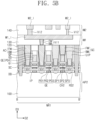
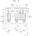
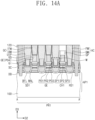
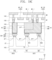
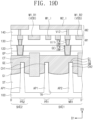
- a semiconductor device may include a substrate including a PMOSFET region and an NMOSFET region, a first active pattern on the PMOSFET region and a second active pattern on the NMOSFET region, a first channel pattern and a first source/drain pattern on the first active pattern, a second channel pattern and a second source/drain pattern on the second active pattern, a gate electrode on the first and second channel patterns, a gate insulating layer between the gate electrode and the first and second channel patterns, a gate spacer on a side surface of the gate electrode, a gate capping pattern on a top surface of the gate electrode, a gate cutting pattern penetrating the gate electrode, an interlayer insulating layer on the gate capping pattern and the gate cutting pattern, an active contact that penetrates the interlayer insulating layer and is electrically connected to the first and second source/drain patterns, metal-semiconductor compound layers between the active contact and the first and second source/drain patterns, respectively, a gate contact that
- the second metal layer may include second interconnection lines electrically connected to the first metal layer.
- the active contact may include a first barrier metal and a first filler metal on the first barrier metal
- the gate contact may include a second barrier metal and a second filler metal on the second barrier metal.
- a proportion of a body-centered cubic (BCC) structure in the first filler metal may be higher than a proportion of a body-centered cubic (BCC) structure in the second filler metal.
- a method of fabricating a semiconductor device may include forming an active pattern on a substrate, forming a sacrificial pattern, which extends in a first direction, on the active pattern, forming a source/drain pattern, which includes a sacrificial layer, at a side of the sacrificial pattern, forming an interlayer insulating layer on the sacrificial pattern and the source/drain pattern, replacing the sacrificial pattern with a gate electrode, forming a contact trench in the interlayer insulating layer, such that at least a portion of the source/drain pattern is free of the interlayer insulating layer, and forming an active contact in the contact trench.
- the forming of the active contact may include forming a barrier metal layer in the contact trench, performing a plasma-using ion bombardment process on the barrier metal layer, and forming a filler metal layer on the barrier metal layer.
- a proportion of a body-centered cubic (BCC) structure in the filler metal layer may range from 60% to 99%.
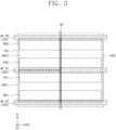
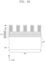
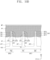
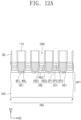
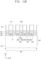
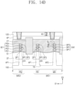
- FIGS. 1 to 3 are conceptual diagrams illustrating logic cells of a semiconductor device according to an embodiment of the inventive concept.
- a single height cell SHC may be provided.
- a first power line M1_R1 and a second power line M1_R2 may be provided on a substrate 100.
- the first power line M1_R1 may be a conduction path, to which a drain voltage VDD (e.g., a power voltage) is provided.
- the second power line M1_R2 may be a conduction path, to which a source voltage VSS (e.g., a ground voltage) is provided.
- VDD drain voltage
- VSS e.g., a ground voltage
- the single height cell SHC may be defined between the first power line M1_R1 and the second power line M1_R2.
- the single height cell SHC may include one PMOSFET region PR and one NMOSFET region NR.
- the single height cell SHC may have a CMOS structure provided between the first and second power lines M1_R1 and M1_R2.
- Each of the PMOSFET and NMOSFET regions PR and NR may have a first width W1 in a first direction D1.
- the widths of the PR and NR regions may be different I the first direction D1.
- a length of the single height cell SHC in the first direction D1 may be defined as a first height HE1.
- the first height HE1 may be substantially equal to a distance (e.g., a pitch) between the first and second power lines M1_R1 and M1_R2.
- the single height cell SHC may constitute a single logic cell.
- the logic cell may mean a logic device (e.g., AND, OR, XOR, XNOR, inverter, and so forth), which is configured to execute a specific function.
- the logic cell may include transistors constituting the logic device and interconnection lines connecting transistors to each other.
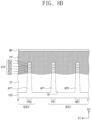
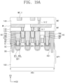
- a double height cell DHC may be provided.
- the first power line M1_R1, the second power line M1_R2, and a third power line M1_R3 may be provided on the substrate 100.
- the first power line M1_R1 may be disposed between the second power line M1_R2 and the third power line M1_R3.
- the third power line M1_R3 may be a conduction path, to which the drain voltage VDD is provided.
- the double height cell DHC may be defined between the second power line M1_R2 and the third power line M1_R3.
- the double height cell DHC may include a first PMOSFET region PR1, a second PMOSFET region PR2, a first NMOSFET region NR1, and a second NMOSFET region NR2.
- the first NMOSFET region NR1 may be adjacent to the second power line M1_R2.
- the second NMOSFET region NR2 may be adjacent to the third power line M1_R3.
- the first and second PMOSFET regions PR1 and PR2 may be adjacent to the first power line M1_R1.
- the first power line M1_R1 When viewed in a plan view, the first power line M1_R1 may be disposed between the first and second PMOSFET regions PR1 and PR2.
- a length of the double height cell DHC in the first direction D1 may be defined as a second height HE2.
- the second height HE2 may be about two times the first height HE1 of FIG. 1 .
- the first and second PMOSFET regions PR1 and PR2 of the double height cell DHC may be combined to constitute as a single PMOSFET region.
- a channel size of a PMOS transistor of the double height cell DHC may be greater than a channel size of a PMOS transistor of the single height cell SHC previously described with reference to FIG. 1 .
- the channel size of the PMOS transistor of the double height cell DHC may be about two times the channel size of the PMOS transistor of the single height cell SHC.
- the double height cell DHC may be operated at a higher speed than the single height cell SHC.
- the double height cell DHC shown in FIG. 2 may be defined as a multi-height cell.
- the multi-height cell may include a triple height cell whose cell height is about three times that of the single height cell SHC.
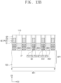
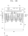
- a first single height cell SHC1, a second single height cell SHC2, and the double height cell DHC may be two-dimensionally disposed on the substrate 100.
- the first single height cell SHC1 may be disposed between the first and second power lines M1_R1 and M1_R2.
- the second single height cell SHC2 may be disposed between the first and third power lines M1_R1 and M1_R3.
- the second single height cell SHC2 may be adjacent to the first single height cell SHC1 in the first direction D1.
- the double height cell DHC may be disposed between the second and third power lines M1_R2 and M1_R3.
- the double height cell DHC may be adjacent to the first and second single height cells SHC1 and SHC2 in a second direction D2.
- a division structure DB may be provided between the first single height cell SHC1 and the double height cell DHC and between the second single height cell SHC2 and the double height cell DHC.
- the active region of the double height cell DHC may be electrically separated from the active region of each of the first and second single height cells SHC1 and SHC2 by the division structure DB.
- FIG. 4 is a plan view illustrating a semiconductor device according to an embodiment of the inventive concept.
- FIGS. 5A to 5D are sectional views, which are respectively taken along lines A-A', B-B', C-C', and D-D' of FIG. 4 .
- FIG. 6 is an enlarged sectional view illustrating a portion 'M' of FIG. 5A .
- FIGS. 4 and 5A to 5D illustrate an example of a detailed structure of the first and second single height cells SHC1 and SHC2 of FIG. 3 .
- the first and second single height cells SHC1 and SHC2 may be provided on the substrate 100.
- Logic transistors constituting the logic circuit may be disposed on each of the first and second single height cells SHC1 and SHC2.
- the substrate 100 may be a semiconductor substrate that is formed of or includes one or more materials, such as silicon, germanium, silicon germanium, a compound semiconductor material, or the like. In an embodiment, the substrate 100 may be a silicon wafer.
- the substrate 100 may include the first PMOSFET region PR1, the second PMOSFET region PR2, the first NMOSFET region NR1, and the second NMOSFET region NR2.
- Each of the first PMOSFET region PR1, the second PMOSFET region PR2, the first NMOSFET region NR1, and the second NMOSFET region NR2 may extend in the second direction D2.
- the first single height cell SHC1 may include the first NMOSFET region NR1 and the first PMOSFET region PR1
- the second single height cell SHC2 may include the second PMOSFET region PR2 and the second NMOSFET region NR2.
- a first active pattern AP1 and a second active pattern AP2 may be defined by a trench TR, which is formed in an upper portion of the substrate 100.
- the first active pattern AP1 may be provided on each of the first and second PMOSFET regions PR1 and PR2.
- the second active pattern AP2 may be provided on each of the first and second NMOSFET regions NR1 and NR2.
- the first and second active patterns AP1 and AP2 may extend in the second direction D2.
- Each of the first and second active patterns AP1 and AP2 may be a vertically-protruding portion of the substrate 100, i.e., extending in the D3 direction or a direction normal to an upper surface of the substrate 100.
- a device isolation layer ST may be provided to at least partially fill the trench TR.
- the device isolation layer ST may include a silicon oxide layer.
- the device isolation layer ST may not cover first and second channel patterns CH1 and CH2, i.e., at least a portion of the first and second channel patterns CH1 and CH2 may be free of the device isolation layer ST as will be described below.
- the first channel pattern CH1 may be provided on the first active pattern AP1.
- the second channel pattern CH2 may be provided on the second active pattern AP2.
- Each of the first and second channel patterns CH1 and CH2 may include a first semiconductor pattern SP1, a second semiconductor pattern SP2, and a third semiconductor pattern SP3, which are sequentially stacked.
- the first to third semiconductor patterns SP1, SP2, and SP3 may be spaced apart from each other in a vertical direction (i.e., a third direction D3 or a direction normal to an upper surface of the substrate 100).
- Each of the first to third semiconductor patterns SP1, SP2, and SP3 may be formed of or include at least one of silicon (Si), germanium (Ge), or silicon germanium (SiGe).
- each of the first to third semiconductor patterns SP1, SP2, and SP3 may be formed of or include crystalline silicon.
- a plurality of first source/drain patterns SD1 may be provided on the first active pattern AP1.
- a plurality of first recesses RS1 may be formed in an upper portion of the first active pattern AP1.
- the first source/drain patterns SD1 may be provided in the first recesses RS1, respectively.
- the first source/drain patterns SD1 may be impurity regions of a first conductivity type (e.g., p-type).
- the first channel pattern CH1 may be interposed between each pair of the first source/drain patterns SD1. In other words, each pair of the first source/drain patterns SD1 may be connected to each other by the stacked first to third semiconductor patterns SP1, SP2, and SP3.
- a plurality of second source/drain patterns SD2 may be provided on the second active pattern AP2.
- a plurality of second recesses RS2 may be formed in an upper portion of the second active pattern AP2.
- the second source/drain patterns SD2 may be provided in the second recesses RS2, respectively.
- the second source/drain patterns SD2 may be impurity regions of a second conductivity type (e.g., n-type).
- the second channel pattern CH2 may be interposed between each pair of the second source/drain patterns SD2. In other words, each pair of the second source/drain patterns SD2 may be connected to each other by the stacked first to third semiconductor patterns SP1, SP2, and SP3.
- the first and second source/drain patterns SD1 and SD2 may be epitaxial patterns, which are formed by a selective epitaxial growth (SEG) process.
- each of the first and second source/drain patterns SD1 and SD2 may have a top surface that is higher than a top surface of the third semiconductor pattern SP3 in the D3 direction and in a cross-sectional view with the substrate 100 serving as a base reference layer.
- a top surface of at least one of the first and second source/drain patterns SD1 and SD2 may be located at substantially the same level as the top surface of the third semiconductor pattern SP3 in the D3 direction.
- the first source/drain patterns SD1 may include a semiconductor material (e.g., SiGe) whose lattice constant is greater than that of the substrate 100.
- the pair of the first source/drain patterns SD1 may exert a compressive stress on the first channel patterns CH1 therebetween.
- the second source/drain patterns SD2 may be formed of or include the same semiconductor element (e.g., Si) as the substrate 100.
- Each of the first source/drain patterns SD1 may include a buffer layer BFL and a main layer MAL on the buffer layer BFL.
- a sectional shape of the first source/drain pattern SD1 in the second direction D2 will be described in more detail with reference to FIG. 5A .
- the buffer layer BFL may be on and at least partially cover an inner surface of the first recess RS1.
- the buffer layer BFL may have a decreasing thickness in an upward direction, i.e., the D3 direction or a direction normal to an upper surface of the substrate 100.
- a thickness of the buffer layer BFL which is measured in the third direction D3 on a bottom of the first recess RS1
- a thickness of the buffer layer BFL which is measured in the second direction D2 at a top level of the first recess RS1.
- the buffer layer BFL may have a 'U'-shaped section along a profile of the first recess RS1.
- the main layer MAL may fill most of an unfilled region of the first recess RS1 having the buffer layer BFL therein.
- a volume of the main layer MAL may be larger than a volume of the buffer layer BFL. That is, a ratio of the volume of the main layer MAL to a total volume of the first source/drain pattern SD1 may be greater than a ratio of the volume of the buffer layer BFL to a total volume of the first source/drain pattern SD1.
- Each of the buffer and main layers BFL and MAL may be formed of or include silicon germanium (SiGe).
- the buffer layer BFL may contain a relatively low concentration of germanium (Ge).
- the buffer layer BFL may contain only silicon (Si), without germanium (Ge).
- a germanium concentration of the buffer layer BFL may range from 0 at% to 10 at%. More specifically, the germanium concentration of the buffer layer BFL may range from 2 at% to 8 at%.
- the main layer MAL may contain a relatively high concentration of germanium (Ge).
- a germanium concentration of the main layer MAL may range from 30 at% to 70 at%.
- the germanium concentration of the main layer MAL may increase in the third direction D3.
- a portion of the main layer MAL, which is adjacent to the buffer layer BFL, may have a germanium concentration of about 40 at%, and an upper portion of the main layer MAL may have a germanium concentration of about 60 at%.
- Each of the buffer and main layers BFL and MAL may contain an impurity (e.g., boron, gallium, or indium) that allows the first source/drain pattern SD1 to have a p-type conductivity.
- the impurity concentration of each of the buffer and main layers BFL and MAL may range from 1E18 atoms/cm 3 to 5E22 atoms/cm 3 .
- An impurity concentration of the main layer MAL may be greater than an impurity concentration of the buffer layer BFL.
- the buffer layer BFL may prevent or reduce the likelihood of a stacking fault between the substrate 100 (i.e., the first active pattern AP1) and the main layer MAL and between the first to third semiconductor patterns SP1, SP2, and SP3 and the main layer MAL.
- the stacking fault may lead to an increase of a channel resistance.
- the stacking fault may easily occur on the bottom of the first recess RS1.
- the buffer layer BFL may be provided to have a relatively large thickness near the bottom of the first recess RS1.
- the buffer layer BFL may protect the main layer MAL from a process of replacing sacrificial layers SAL, which will be described below, with the first to third portions PO1, PO2, and PO3 of the gate electrode GE.
- the buffer layer BFL may prevent or inhibit an etchant material, which is used to remove the sacrificial layers SAL, from entering and etching the main layer MAL.
- the gate electrodes GE may extend in the first direction D1 and may cross the first and second channel patterns CH1 and CH2.
- the gate electrodes GE may be arranged at a first pitch in the second direction D2.
- Each of the gate electrodes GE may overlap the first and second channel patterns CH1 and CH2 in the vertical or D3 direction.
- the gate electrode GE may include a first portion PO1 interposed between the active pattern AP1 or AP2 and the first semiconductor pattern SP1, a second portion PO2 interposed between the first and second semiconductor patterns SP1 and SP2, a third portion PO3 interposed between the second and third semiconductor patterns SP2 and SP3, and a fourth portion PO4 on the third semiconductor pattern SP3.
- the first to third portions PO1, PO2, and PO3 of the gate electrode GE on the PMOSFET region PR may have different widths from each other in the D2 direction.
- the largest width of the third portion PO3 in the second direction D2 may be larger than the largest width of the second portion PO2 in the second direction D2.
- the largest width of the first portion PO1 in the second direction D2 may be larger than the largest width of the third portion PO3 in the second direction D2.
- the gate electrode GE may be provided on a top surface TS, a bottom surface BS, and opposite side surfaces SW of each of the first to third semiconductor patterns SP1, SP2, and SP3. That is, the transistor according to the present embodiment may be a three-dimensional field effect transistor (e.g., MBCFET or GAAFET) in which the gate electrode GE is provided to three-dimensionally surround the channel pattern.
- MBCFET MBCFET
- GAAFET three-dimensional field effect transistor
- the first single height cell SHC1 may have a first border BD1 and a second border BD2, which are opposite to each other in the second direction D2.
- the first and second borders BD1 and BD2 may be extended in the first direction D1.
- the first single height cell SHC1 may have a third border BD3 and a fourth border BD4, which are opposite to each other in the first direction D1.
- the third and fourth borders BD3 and BD4 may be extended in the second direction D2.
- Gate cutting patterns CT may be disposed on a border, which is parallel to the second direction D2, of each of the first and second single height cells SHC1 and SHC2.
- the gate cutting patterns CT may be disposed on the third and fourth borders BD3 and BD4 of the first single height cell SHC1.
- the gate cutting patterns CT may be arranged at the first pitch along the third border BD3.
- the gate cutting patterns CT may be arranged at the first pitch along the fourth border BD4.
- the gate cutting patterns CT on the third and fourth borders BD3 and BD4 may overlap the gate electrodes GE, respectively, in the D3 direction.
- the gate cutting patterns CT may be formed of or include one or more insulating materials (e.g., silicon oxide, silicon nitride, or combinations thereof).
- the gate electrode GE on the first single height cell SHC1 may be separated from the gate electrode GE on the second single height cell SHC2 by the gate cutting pattern CT.
- the gate cutting pattern CT may be interposed between the gate electrodes GE on the first and second single height cells SHC1 and SHC2 which are aligned to each other in the first direction D1. That is, the gate electrode GE extending in the first direction D1 may be divided into a plurality of the gate electrodes GE by the gate cutting patterns CT.
- a pair of gate spacers GS may be respectively disposed on opposite side surfaces of the fourth portion PO4 of the gate electrode GE.
- the gate spacers GS may extend along the gate electrode GE and in the first direction D1. Top surfaces of the gate spacers GS may be higher than a top surface of the gate electrode GE in the D3 direction with the substrate 100 serving as a base reference layer.
- the top surfaces of the gate spacers GS may be coplanar with a top surface of a first interlayer insulating layer 110, which will be described below.
- the gate spacers GS may be formed of or include at least one of SiCN, SiCON, or SiN.
- the gate spacers GS may be a multi-layered structure, which is formed of or includes at least two different materials selected from SiCN, SiCON, and SiN.
- a gate capping pattern GP may be provided on the gate electrode GE.
- the gate capping pattern GP may extend along the gate electrode GE or in the first direction D1.
- the gate capping pattern GP may be formed of or include a material having an etch selectivity with respect to first and second interlayer insulating layers 110 and 120, which will be described below.
- the gate capping pattern GP may be formed of or include at least one of SiON, SiCN, SiCON, or SiN.
- a gate insulating layer GI may be interposed between the gate electrode GE and the first channel pattern CH1 and between the gate electrode GE and the second channel pattern CH2.
- the gate insulating layer GI may be on and at least partially cover the top surface TS, the bottom surface BS, and the opposite side surfaces SW of each of the first to third semiconductor patterns SP1, SP2, and SP3.
- the gate insulating layer GI may be on and at least partially cover a top surface of the device isolation layer ST below the gate electrode GE.
- the gate insulating layer GI may include a silicon oxide layer, a silicon oxynitride layer, and/or a high-k dielectric layer.
- the high-k dielectric layer may be formed of or include one or more high-k dielectric materials whose dielectric constants are higher than that of silicon oxide.
- the high-k dielectric material may include at least one of hafnium oxide, hafnium silicon oxide, hafnium zirconium oxide, hafnium tantalum oxide, lanthanum oxide, zirconium oxide, zirconium silicon oxide, tantalum oxide, titanium oxide, barium strontium titanium oxide, barium titanium oxide, strontium titanium oxide, lithium oxide, aluminum oxide, lead scandium tantalum oxide, or lead zinc niobate.
- the semiconductor device may include a negative capacitance (NC) FET using a negative capacitor.
- the gate insulating layer GI may include a ferroelectric layer exhibiting a ferroelectric property and a paraelectric layer exhibiting a paraelectric property.
- the ferroelectric layer may have a negative capacitance, and the paraelectric layer may have a positive capacitance.
- a total capacitance may be reduced to a value that is less than a capacitance of each of the capacitors.
- a total capacitance of the serially-connected capacitors may have a positive value and may be greater than an absolute value of each capacitance.
- a total capacitance of the serially-connected ferroelectric and paraelectric layers may be increased. Due to such an increase of the total capacitance, a transistor including the ferroelectric layer may have a subthreshold swing (SS), which is less than 60 mV/decade, at room temperature.
- SS subthreshold swing
- the ferroelectric layer may have a ferroelectric property.
- the ferroelectric layer may be formed of or include at least one of, for example, hafnium oxide, hafnium zirconium oxide, barium strontium titanium oxide, barium titanium oxide, and/or lead zirconium titanium oxide.
- the hafnium zirconium oxide may be hafnium oxide that is doped with zirconium (Zr).
- the hafnium zirconium oxide may be a compound composed of hafnium (Hf), zirconium (Zr), and/or oxygen (O).
- the ferroelectric layer may further include dopants.
- the dopants may include at least one of aluminum (Al), titanium (Ti), niobium (Nb), lanthanum (La), yttrium (Y), magnesium (Mg), silicon (Si), calcium (Ca), cerium (Ce), dysprosium (Dy), erbium (Er), gadolinium (Gd), germanium (Ge), scandium (Sc), strontium (Sr), and/or tin (Sn).
- the kind of the dopants in the ferroelectric layer may vary depending on a ferroelectric material included in the ferroelectric layer.
- the dopants in the ferroelectric layer may include at least one of, for example, gadolinium (Gd), silicon (Si), zirconium (Zr), aluminum (Al), and/or yttrium (Y).
- Gd gadolinium
- Si silicon
- Zr zirconium
- Al aluminum
- Y yttrium
- a content of aluminum in the ferroelectric layer may range from 3 to 8 at% (atomic percentage).
- the content of the dopants e.g., aluminum atoms
- the content of the dopants may be a ratio of the number of aluminum atoms to the number of hafnium and aluminum atoms.
- a content of silicon in the ferroelectric layer may range from 2 at% to 10 at%.
- a content of yttrium in the ferroelectric layer may range from 2 at% to 10 at%.
- a content of gadolinium in the ferroelectric layer may range from 1 at% to 7 at%.
- the dopants are zirconium (Zr)
- a content of zirconium in the ferroelectric layer may range from 50 at% to 80 at%.
- the paraelectric layer may have a paraelectric property.
- the paraelectric layer may be formed of or include at least one of, for example, silicon oxide and/or high-k metal oxides.
- the metal oxides, which can be used as the paraelectric layer may include at least one of, for example, hafnium oxide, zirconium oxide, and/or aluminum oxide, but embodiments of the inventive concept are not limited to these examples.
- the ferroelectric layer and the paraelectric layer may be formed of or include the same material.
- the ferroelectric layer may have a ferroelectric property, but the paraelectric layer may not have a ferroelectric property.
- a crystal structure of the hafnium oxide in the ferroelectric layer may be different from a crystal structure of the hafnium oxide in the paraelectric layer.
- the ferroelectric layer may exhibit a ferroelectric property only when its thickness is in a specific range.
- the ferroelectric layer may have a thickness ranging from 0.5 to 10 nm, but embodiments of the inventive concept are not limited to this example. Because a critical thickness associated with the occurrence of the ferroelectric property varies depending on the kind of the ferroelectric material, the thickness of the ferroelectric layer may be changed depending on the kind of the ferroelectric material.
- the gate insulating layer GI may include a single ferroelectric layer.
- the gate insulating layer GI may include a plurality of ferroelectric layers spaced apart from each other.
- the gate insulating layer GI may have a multi-layered structure, in which a plurality of ferroelectric layers and a plurality of paraelectric layers are alternately stacked.
- the gate electrode GE may include a first metal pattern and a second metal pattern on the first metal pattern.
- the first metal pattern may be provided on the gate insulating layer GI and may be adjacent to the first to third semiconductor patterns SP1, SP2, and SP3.
- the first metal pattern may include a work-function metal, which can be used to adjust a threshold voltage of the transistor. By adjusting a thickness and composition of the first metal pattern, it may be possible to realize a transistor having a desired threshold voltage.
- the first to third portions PO1, PO2, and PO3 of the gate electrode GE may be composed of the first metal pattern or the work-function metal.
- the first metal pattern may include a metal nitride layer.
- the first metal pattern may include a layer that is composed of at least one metallic material, which is selected from the group consisting of titanium (Ti), tantalum (Ta), aluminum (Al), tungsten (W) and molybdenum (Mo), and nitrogen (N).
- the first metal pattern may further include carbon (C).
- the first metal pattern may include a plurality of work function metal layers, which are stacked.
- the second metal pattern may be formed of or include a metallic material whose resistance is lower than the first metal pattern.
- the second metal pattern may be formed of or include at least one metallic material, which is selected from the group consisting of tungsten (W), aluminum (Al), titanium (Ti), and tantalum (Ta).
- the fourth portion PO4 of the gate electrode GE may include the first metal pattern and the second metal pattern on the first metal pattern.
- inner spacers IP may be provided on the first and second NMOSFET regions NR1 and NR2. That is, the inner spacers IP may be provided on the second active pattern AP2.
- the inner spacers IP may be respectively interposed between the first to third portions PO1, PO2, and PO3 of the gate electrode GE and the second source/drain pattern SD2.
- the inner spacers IP may be in direct contact with the second source/drain pattern SD2.
- Each of the first to third portions PO1, PO2, and PO3 of the gate electrode GE may be spaced apart from the second source/drain pattern SD2 by the inner spacerIP.
- a first interlayer insulating layer 110 may be provided on the substrate 100.
- the first interlayer insulating layer 110 may be on and at least partially cover the gate spacers GS and the first and second source/drain patterns SD1 and SD2.
- the first interlayer insulating layer 110 may have a top surface that is substantially coplanar with the top surface of the gate capping pattern GP and the top surface of the gate spacer GS.
- a second interlayer insulating layer 120 may be formed on the first interlayer insulating layer 110 to be on and at least partially cover the gate capping pattern GP.
- a third interlayer insulating layer 130 may be provided on the second interlayer insulating layer 120.
- a fourth interlayer insulating layer 140 may be provided on the third interlayer insulating layer 130.
- at least one of the first to fourth interlayer insulating layers 110 to 140 may include a silicon oxide layer.
- a pair of division structures DB may be provided at both sides of each of the first and second single height cells SHC1 and SHC2 to be opposite to each other in the second direction D2.
- pair of the division structures DB may be respectively provided on the first and second borders BD1 and BD2 of the first single height cell SHC1.
- the division structure DB may extend in the first direction D1 to be parallel to the gate electrodes GE.
- a pitch between the division structure DB and the gate electrode GE adjacent thereto may be equal to the first pitch.
- the division structure DB may penetrate the first and second interlayer insulating layers 110 and 120 and may extend into the first and second active patterns AP1 and AP2.
- the division structure DB may penetrate an upper portion of each of the first and second active patterns AP1 and AP2.
- the division structure DB may electrically separate an active region of each of the first and second single height cells SHC1 and SHC2 from an active region of a neighboring cell.
- Active contacts AC may penetrate the first and second interlayer insulating layers 110 and 120 and may be electrically connected to the first and second source/drain patterns SD1 and SD2, respectively.
- a pair of the active contacts AC may be respectively provided at both sides of the gate electrode GE.
- the active contact AC When viewed in a plan view, the active contact AC may be a bar-shaped pattern that extends in the first direction D1.
- the active contact AC may be a self-aligned contact.
- the active contact AC may be formed by a self-alignment process using the gate capping pattern GP and the gate spacer GS.
- the active contact AC may be on and cover at least a portion of the side surface of the gate spacer GS.
- the active contact AC may be on and at least partially cover a portion of the top surface of the gate capping pattern GP.
- Metal-semiconductor compound layers SC may be respectively interposed between the active contact AC and the first source/drain pattern SD1 and between the active contact AC and the second source/drain pattern SD2.
- the active contact AC may be electrically connected to the source/drain pattern SD1 and SD2 through the metal-semiconductor compound layer SC.
- the metal-semiconductor compound layer SC may be formed of or include at least one of titanium silicide, tantalum silicide, tungsten silicide, nickel silicide, or cobalt silicide.
- At least one active contact AC on the first single height cell SHC1 may electrically connect the first source/drain pattern SD1 of the first PMOSFET region PR1 to the second source/drain pattern SD2 of the first NMOSFET region NR1.
- the active contact AC may extend from the second source/drain pattern SD2 of the first NMOSFET region NR1 to the first source/drain pattern SD1 of the first PMOSFET region PR1 in the first direction D1.
- Gate contacts GC may penetrate the second interlayer insulating layer 120 and the gate capping pattern GP and may be electrically connected to the gate electrodes GE, respectively.
- two gate contacts GC on the first single height cell SHC1 may overlap the first PMOSFET region PR1 in the D3 direction. That is, the two gate contacts GC on the first single height cell SHC1 may be provided on the first active pattern AP1 (e.g., see FIG. 5A ).
- a single gate contact GC on the first single height cell SHC1 may overlap the first NMOSFET region NR1 in the D3 direction. In other words, the single gate contact GC on the first single height cell SHC1 may be provided on the second active pattern AP2 (e.g., see FIG. 5B ).
- the gate contact GC may be freely disposed on the gate electrode GE, without any limitation in its position.
- the gate contacts GC on the second single height cell SHC2 may be respectively disposed on the second PMOSFET region PR2, the second NMOSFET region NR2, and the device isolation layer ST at least partially filling the trench TR (e.g., see FIG. 4 ).
- an upper portion of the active contact AC adjacent to the gate contact GC may be at least partially filled with an upper insulating pattern UIP.
- a bottom surface of the upper insulating pattern UIP may be lower than a bottom surface of the gate contact GC in the D3 direction with the substrate 100 serving as a base reference layer.
- a top surface of the active contact AC adjacent to the gate contact GC may be formed at a level, which is lower than the bottom surface of the gate contact GC in the D3 direction with the substrate 100 serving as a base reference layer, by the upper insulating pattern UIP. Accordingly, it may be possible to prevent or reduce the likelihood of the gate contact GC and the active contact AC, which are adjacent to each other, from being in contact with each other and thereby to prevent or reduce the likelihood of a short circuit issue from occurring therebetween.
- Each of the active and gate contacts AC and GC may include a barrier metal BM and a filler metal FM on the barrier metal BM.
- the barrier metal BM may be provided to enclose all surfaces of the filler metal FM except for a top surface.
- the filler metal FM may be formed of or include at least one of molybdenum, tungsten, ruthenium, cobalt, or vanadium.
- the filler metal FM may be formed of or include molybdenum.
- the barrier metal BM may include a metal nitride layer.
- the metal nitride layer may be formed of or include at least one of titanium nitride (TiN), tantalum nitride (TaN), tungsten nitride (WN), nickel nitride (NiN), cobalt nitride (CoN), or platinum nitride (PtN).
- TiN titanium nitride
- TaN tantalum nitride
- WN tungsten nitride
- NiN nickel nitride
- CoN cobalt nitride
- PtN platinum nitride
- a first metal layer M1 may be provided in the third interlayer insulating layer 130.
- the first metal layer M1 may include the first power line M1_R1, the second power line M1_R2, the third power line M1_R3, and first interconnection lines M1_I.
- the interconnection lines M1_R1, M1_R2, M1_R3, and M1_I of the first metal layer M1 may extend in the second direction D2 to be parallel to each other.
- first and second power lines M1_R1 and M1_R2 may be provided on the third and fourth borders BD3 and BD4 of the first single height cell SHC1, respectively.
- the first power line M1_R1 may extend along the third border BD3 and in the second direction D2.
- the second power line M1_R2 may extend along the fourth border BD4 and in the second direction D2.
- the first interconnection lines M1_I of the first metal layer M1 may be arranged at a second pitch in the first direction D1.
- the second pitch may be smaller than the first pitch.
- a linewidth of each of the first interconnection lines M1_I may be smaller than a linewidth of each of the first to third power lines M1_R1, M1_R2, and M1_R3 in the D1 direction as shown in FIG. 5C .
- the first metal layer M1 may further include first vias VI1.
- the first vias VI1 may be respectively provided below (i.e., closer to the substrate 100) the interconnection lines M1_R1, M1_R2, M1_R3, and M1_I of the first metal layer M1.
- the active contact AC and the interconnection line of the first metal layer M1 may be electrically connected to each other through the first via VI1.
- the gate contact GC and the interconnection line of the first metal layer M1 may be electrically connected to each other through the first via VI1.
- the first via VI1 may include the barrier metal BM and the filler metal FM on the barrier metal BM, like the active and gate contacts AC and GC.
- the interconnection line of the first metal layer M1 and the first via VI1 thereunder may be formed by separate processes.
- the interconnection line and the first via VI1 of the first metal layer M1 may be independently formed by respective single damascene processes.
- the semiconductor device according to the present embodiment may be fabricated using a sub-20 nm process.
- a second metal layer M2 may be provided in the fourth interlayer insulating layer 140.
- the second metal layer M2 may include a plurality of second interconnection lines M2_I.
- Each of the second interconnection lines M2_I of the second metal layer M2 may be a line- or bar-shaped pattern that extend in the first direction D1. In other words, the second interconnection lines M2_I may extend in the first direction D1 and parallel to each other.
- the second metal layer M2 may further include second vias VI2, which are respectively provided below (i.e., closer to the substrate) the second interconnection lines M2_I.
- the interconnection lines of the first and second metal layers M1 and M2 may be electrically connected to each other through the second via VI2.
- the interconnection line of the second metal layer M2 and the second via VI2 thereunder may be formed together by a dual damascene process.
- the interconnection lines of the first metal layer M1 may be formed of or include a conductive material that is the same as or different from those of the second metal layer M2.
- the interconnection lines of the first and second metal layers M1 and M2 may be formed of or include one or more metallic materials (e.g., copper, ruthenium, aluminum, tungsten, molybdenum, and cobalt).
- a plurality of metal layers e.g., M3, M4, M5, and so forth
- Each of the stacked metal layers may include interconnection lines, which are used as routing paths between cells.
- the barrier metal BM may be provided on an inner surface of a contact trench CNH of the first interlayer insulating layer 110.
- the barrier metal BM may have a uniform thickness.
- the barrier metal BM may include a metal nitride layer (e.g., TiN) formed by a PECVD process.
- the barrier metal BM may include a metal nitride layer (e.g., TiN), which is formed using a deposition process and then is treated using plasma.
- the barrier metal BM may be or include a metal nitride layer that is treated by a plasma-using ion bombardment process which is performed during or directly after its deposition process.
- the material (e.g., TiN) of the barrier metal BM may be denser than a TiN layer deposited using a simple CVD process. Since the material (e.g., TiN) of the barrier metal BM has an increased density by the ion bombardment process, it may have a compressive stress.
- the filler metal FM may be formed through a deposition process (e.g., ALD), which is performed on the barrier metal BM after the formation of the barrier metal BM. During the formation of the filler metal FM, a crystal structure of the filler metal FM may be affected by the barrier metal BM.
- ALD atomic layer deposition
- the filler metal FM may be molybdenum and may include a first crystalline region CRS1 and a second crystalline region CRS2.
- the first crystalline region CRS1 may have a first crystal structure (e.g., a body-centered cubic (BCC) structure).
- the second crystalline region CRS2 may have a second crystal structure (e.g., a face-centered cubic (FCC) structure).
- a grain boundary GRB may be defined between the crystalline regions.
- the grain boundary GRB may be formed between the first and second crystalline regions CRS1 and CRS2 having different crystalline structures.
- the grain boundary GRB may be formed between the first crystalline regions CRS1, which are adjacent to each other and have the same crystalline structure.
- a proportion of the first crystalline regions CRS1 in the filler metal FM may range from 60% to 99%.
- a ratio of a volume of the first crystalline regions CRS1 to a total volume of the filler metal FM may range from 60% to 99%.
- a ratio of an area of the first crystalline regions CRS1 to a total area of the filler metal FM may range from 60% to 99%.
- a fraction or proportion of the BCC structure in the filler metal FM may range from 60% to 99%.
- the second crystalline region CRS2 may correspond to a remaining region of the filler metal FM except for the first crystalline regions CRS1.
- 60% to 99% of a crystal structure in the filler metal FM may be a BCC structure. More specifically, 80% to 99% of a crystal structure in the filler metal FM (i.e., molybdenum) may be a BCC structure.
- the filler metal FM may have a resistivity of 16 ⁇ cm to 18 ⁇ cm.
- the filler metal FM since the proportion of the BCC structure in the filler metal FM is higher than 80%, the filler metal FM may have a relatively low resistivity. That is, the active contact AC may have a relatively low resistance, and this may make it possible to improve electrical characteristics of the semiconductor device.
- the gate contact GC and the first via VI1 may also include the barrier and filler metals BM and FM, and in this case, the barrier and filler metals BM and FM in the gate contact GC and the first via VI1 may have the same features as those of the active contact AC described above.
- the transistors constituting the logic circuit may be connected to the interconnection lines of the first metal layer M1 thereon with a reduced electric resistance, and this may make it possible to improve electrical characteristics of the semiconductor device.
- a proportion of the body-centered cubic (BCC) structure in the filler metal FM of the active contact AC may be higher than a proportion of the body-centered cubic (BCC) structure in the filler metal FM of each of the gate contact GC and the first via VI1.
- resistivity of the filler metal FM may be lower in the active contact AC than in each of the gate contact GC and the first via VI1.
- FIGS. 7A to 14D are sectional views illustrating a method of fabricating a semiconductor device according to an embodiment of the inventive concept.
- FIGS. 7A , 8A , 9A , 10A , 11A , 12A , 13A , and 14A are sectional views corresponding to a line A-A' of FIG. 4 .
- FIGS. 9B , 10B , 11B , 12B , 13B , and 14B are sectional views corresponding to a line B-B' of FIG. 4 .
- FIGS. 9C , 10C , 11C , 12C , 13C , and 14C are sectional views corresponding to a line C-C' of FIG. 4 .
- FIGS. 7B , 8B , 9D , 10D , 11D , 12D , 13D , and 14D are sectional views corresponding to a line D-D' of FIG. 4 .
- the substrate 100 may be provided, and in an embodiment, the substrate may include the first and second PMOSFET regions PR1 and PR2 and the first and second NMOSFET regions NR1 and NR2. Active layers ACL and the sacrificial layers SAL may be alternately stacked on the substrate 100.
- the active layers ACL may be formed of or include silicon (Si), germanium (Ge), and/or silicon germanium (SiGe), and the sacrificial layers SAL may be formed of or include silicon (Si), germanium (Ge), and/or silicon germanium (SiGe).
- the sacrificial layer SAL may be formed of or include a material having an etch selectivity with respect to the active layer ACL.
- the active layers ACL may be formed of or include silicon (Si)
- the sacrificial layers SAL may be formed of or include silicon germanium (SiGe).
- a germanium concentration of each of the sacrificial layers SAL may range from 10 at% to 30 at%.
- a patterning process using the mask patterns as an etch mask may be performed to form the trench TR defining the first and second active patterns AP1 and AP2.
- the first active pattern AP1 may be formed on each of the first and second PMOSFET regions PR1 and PR2.
- the second active pattern AP2 may be formed on each of the first and second NMOSFET regions NR1 and NR2.
- a stacking pattern STP may be formed on each of the first and second active patterns AP1 and AP2.
- the stacking pattern STP may include the active layers ACL and the sacrificial layers SAL which are alternately stacked.
- the stacking pattern STP may be formed along with the first and second active patterns AP1 and AP2 during the patterning process.
- the device isolation layer ST may be formed to at least partially fill the trench TR.
- an insulating layer may be formed on the substrate 100 to at least partially cover the first and second active patterns AP1 and AP2 and the stacking patterns STP.
- the device isolation layer ST may be formed by recessing the insulating layer to expose at least a portion of the stacking patterns STP.
- the device isolation layer ST may be formed of or include at least one insulating material (e.g., silicon oxide).
- the stacking patterns STP may be placed above the device isolation layer ST in the D3 direction as shown in FIG. 7B and may be exposed to the outside of the device isolation layer ST. In other words, the stacking patterns STP may protrude vertically, i.e., the D3 direction, above the device isolation layer ST.
- sacrificial patterns PP may be formed on the substrate 100 to cross the stacking patterns STP.
- Each of the sacrificial patterns PP may be a line- or bar-shaped pattern that extends in the first direction D1.
- the sacrificial patterns PP may be arranged at a first pitch in the second direction D2.
- the formation of the sacrificial patterns PP may include forming a sacrificial layer on the substrate 100, forming hard mask patterns MP on the sacrificial layer, and patterning the sacrificial layer using the hard mask patterns MP as an etch mask.
- the sacrificial layer may be formed of or include polysilicon.
- a pair of the gate spacers GS may be formed on opposite side surfaces of each of the sacrificial patterns PP.
- the formation of the gate spacers GS may include conformally forming a gate spacer layer on the substrate 100 and anisotropically etching the gate spacer layer.
- the gate spacer GS may be a multi-layered structure including at least two layers.
- the first recesses RS1 may be formed in the stacking pattern STP on the first active pattern AP1.
- the second recesses RS2 may be formed in the stacking pattern STP on the second active pattern AP2.
- the device isolation layer ST may also be recessed at both sides of each of the first and second active patterns AP1 and AP2 (e.g., see FIG. 9C ).
- the first recesses RS1 may be formed by etching the stacking pattern STP on the first active pattern AP1 using the hard mask patterns MP and the gate spacers GS as an etch mask.
- the first recess RS1 may be formed between a pair of the sacrificial patterns PP.
- the second recesses RS2 in the stacking pattern STP on the second active pattern AP2 may be formed by the same method as that for the first recesses RS1.
- the formation of the second recess RS2 may further include forming the inner spacers IP in recessed regions that are formed by selectively etching the sacrificial layer SAL.
- the first to third semiconductor patterns SP1, SP2, and SP3, which are sequentially stacked between adjacent ones of the first recesses RS1, may be respectively formed from the active layers ACL.
- the first to third semiconductor patterns SP1, SP2, and SP3, which are sequentially stacked between adjacent ones of the second recesses RS2, may be respectively formed from the active layers ACL.
- the first to third semiconductor patterns SP1, SP2, and SP3 between the adjacent ones of the first recesses RS1 may constitute the first channel pattern CH1.
- the first to third semiconductor patterns SP1, SP2, and SP3 between the adjacent ones of the second recesses RS2 may constitute the second channel pattern CH2.
- the buffer layer BFL may contain a semiconductor material (e.g., SiGe) whose lattice constant is greater than that of a semiconductor material of the substrate 100.
- the buffer layer BFL may contain a relatively low concentration of germanium (Ge).
- the buffer layer BFL may contain only silicon (Si) without germanium (Ge).
- the germanium concentration of the buffer layer BFL may range from 0 at% to 10 at%.
- a second SEG process may be performed on the buffer layer BFL to form the main layer MAL.
- the main layer MAL may be formed to at least partially fill the first recess RS1.
- the main layer MAL may contain a relatively high concentration of germanium. In an embodiment, the germanium concentration of the main layer MAL may range from 30 at% to 70 at%.
- the first source/drain pattern SD1 may be doped in-situ with p-type impurities (e.g., boron, gallium, or indium) during the formation of the buffer and main layers BFL and MAL.
- impurities may be injected into the first source/drain pattern SD1, after the formation of the first source/drain pattern SD1.
- the second source/drain pattern SD2 may be doped in-situ with n-type impurities (e.g., phosphorus, arsenic, or antimony). In other embodiments, impurities may be injected into the second source/drain pattern SD2, after the formation of the second source/drain pattern SD2.
- n-type impurities e.g., phosphorus, arsenic, or antimony.
- impurities may be injected into the second source/drain pattern SD2, after the formation of the second source/drain pattern SD2.
- the first interlayer insulating layer 110 may be formed to at least partially cover the first and second source/drain patterns SD1 and SD2, the hard mask patterns MP, and the gate spacers GS.
- the first interlayer insulating layer 110 may include a silicon oxide layer.
- the first interlayer insulating layer 110 may be planarized to at least partially expose the top surfaces of the sacrificial patterns PP.
- the planarization of the first interlayer insulating layer 110 may be performed using an etch-back or chemical-mechanical polishing (CMP) process. Most or all of the hard mask patterns MP may be removed during the planarization process. Accordingly, the first interlayered insulating layer 110 may have a top surface that is coplanar with the top surfaces of the sacrificial patterns PP and the top surfaces of the gate spacers GS.
- CMP chemical-mechanical polishing
- a photolithography process may be performed to selectively open a region of the sacrificial pattern PP.
- a region of the sacrificial pattern PP on the third and fourth borders BD3 and BD4 of the first single height cell SHC1 may be selectively opened.
- the opened region of the sacrificial pattern PP may be selectively etched and removed.
- the gate cutting pattern CT may be formed by at least partially filling a space, which is formed by removing the sacrificial pattern PP, with an insulating material.
- the exposed sacrificial patterns PP may be selectively removed.
- an outer region ORG at least partially exposing the first and second channel patterns CH1 and CH2 may be formed (e.g., see FIG. 12D ).
- the removal of the sacrificial patterns PP may include a wet etching process, which is performed using an etching solution capable of selectively etching polysilicon.
- the sacrificial layers SAL exposed through the outer region ORG may be selectively removed to form inner regions IRG (e.g., see FIG. 12D ).
- the etching process may be chosen to have a high etch rate for a material (e.g., SiGe) having a relatively high germanium concentration.
- the etching process may be chosen to have a high etch rate for a silicon germanium layer whose germanium concentration is higher than 10 at%.
- the sacrificial layers SAL on the first and second PMOSFET regions PR1 and PR2 and the first and second NMOSFET regions NR1 and NR2 may be removed during the etching process.
- the etching process may be a wet etching process.
- An etchant material, which is used in the etching process, may be chosen to remove the sacrificial layer SAL having a relatively high germanium concentration.
- the first source/drain pattern SD1 on the first and second PMOSFET regions PR1 and PR2 may be protected from the etching process by the buffer layer BFL having a relatively low germanium concentration.
- first to third semiconductor patterns SP1, SP2, and SP3, which are stacked on each of the first and second active patterns AP1 and AP2, may be left.
- Empty regions, which are formed by removing the sacrificial layers SAL, may form first to third inner regions IRG1, IRG2, and IRG3, respectively.
- the first inner region IRG1 may be formed between the active pattern AP1 or AP2 and the first semiconductor pattern SP1
- the second inner region IRG2 may be formed between the first semiconductor pattern SP1 and the second semiconductor pattern SP2
- the third inner region IRG3 may be formed between the second semiconductor pattern SP2 and the third semiconductor pattern SP3.
- the gate insulating layer GI may be conformally formed on the exposed first to third semiconductor patterns SP1, SP2, and SP3.
- the gate electrode GE may be formed on the gate insulating layer GI.
- the gate electrode GE may include the first to third portions PO1, PO2, and PO3, which are respectively formed in the first to third inner regions IRG1, IRG2, and IRG3, and the fourth portion PO4, which is formed in the outer region ORG.
- the gate electrode GE may be recessed to have a reduced height. Upper portions of the first and second gate cutting patterns CT1 and CT2 may be slightly recessed, during the recessing of the gate electrode GE.
- the gate capping pattern GP may be formed on the recessed gate electrode GE.
- the second interlayer insulating layer 120 may be formed on the first interlayer insulating layer 110.
- the second interlayer insulating layer 120 may include a silicon oxide layer.
- the active contacts AC may be formed to penetrate the second interlayer insulating layer 120 and the first interlayer insulating layer 110 and to be electrically connected to the first and second source/drain patterns SD1 and SD2.
- the gate contacts GC may be formed to penetrate the second interlayer insulating layer 120 and the gate capping pattern GP and to be electrically connected to the gate electrodes GE, respectively.
- each of the active and gate contacts AC and GC may include forming the barrier metal BM and forming the filler metal FM on the barrier metal BM.
- the barrier metal BM may be conformally formed and may include a metal layer and a metal nitride layer.
- the filler metal FM may be formed of or include one or more low resistance metals.
- a pair of the division structures DB may be formed at both sides of each of the first and second single height cells SHC1 and SHC2.
- the division structure DB may penetrate the second interlayer insulating layer 120 and the gate electrode GE and may extend into the active pattern AP1 or AP2.
- the division structure DB may be formed of or include an insulating material (e.g., silicon oxide or silicon nitride).
- the third interlayer insulating layer 130 may be formed on the active contacts AC and the gate contacts GC.
- the first metal layer M1 may be formed in the third interlayer insulating layer 130.
- the first vias VI1 which are respectively connected to the active and gate contacts AC and GC, may be formed in a lower portion of the third interlayer insulating layer 130.
- Each of the first vias VI1 may include the barrier metal BM and the filler metal FM.
- the interconnection lines M1_R1, M1_R2, M1_R3, and M1_I, which are in contact with the first vias VI1, may be formed in an upper portion of the third interlayer insulating layer 130.
- the fourth interlayer insulating layer 140 may be formed on the third interlayer insulating layer 130.
- the second metal layer M2 may be formed in the fourth interlayer insulating layer 140.
- FIGS. 15 to 17 are enlarged sectional views illustrating a method of forming an active contact in a portion 'M' of FIG. 14A .
- the contact trench CNH may be formed to penetrate the first interlayer insulating layer 110.
- the contact trench CNH may be formed to at least partially expose the first source/drain pattern SD1.
- a bottom of the contact trench CNH may be lower than a top surface of the first source/drain pattern SD1in the D3 direction as shown in FIG. 15 .
- a barrier metal layer BML may be formed to conformally at least partially cover an inner surface of the contact trench CNH.
- the barrier metal layer BML may be formed using a chemical vapor deposition (CVD) process.
- the barrier metal layer BML may include a metal nitride (e.g., TiN) layer.
- the barrier metal layer BML may be formed using plasma.
- the barrier metal layer BML may be formed using a deposition process (e.g., PECVD process), which is performed under plasma environment.
- the barrier metal layer BML may be formed using a deposition process, and then, a plasma-using post-treatment process may be further performed on the barrier metal layer BML.
- the barrier metal layer BML may experience an ion bombardment caused by ions IN in plasma.
- the ions IN may be produced by supplying inactive and/or inert gases (e.g., nitrogen, argon, helium, neon, krypton, and xenon gases) in a process chamber during the plasma process.
- inactive and/or inert gases e.g., nitrogen, argon, helium, neon, krypton, and xenon gases
- the ion IN bombarding of the barrier metal layer BML may include a nitrogen ion.
- the ion IN bombarding of the barrier metal layer BML may include an argon ion.
- argon (Ar) may be left in the barrier metal layer BML and may serve as an impurity.
- the impurity, which is left in the barrier metal layer BML may include argon, helium, neon, krypton, and/or xenon atoms, which are injected in the form of an ion during the plasma process.
- a concentration of the impurity in the barrier metal layer BML may range from 1E18 atoms/cm3 to 1E21 atoms/cm3.
- the barrier metal layer BML may have a high density, compared with a layer that is not exposed to the plasma process.
- the barrier metal layer BML may have compressive stress.
- a filler metal layer FML may be formed on the barrier metal layer BML.
- the filler metal layer FML may be formed using a deposition process (e.g., ALD).
- the filler metal layer FML may be formed of or include at least one of molybdenum, tungsten, ruthenium, cobalt, or vanadium. In an embodiment, the filler metal layer FML may be formed of or include molybdenum.
- the filler metal layer FML may include the first crystalline regions CRS1 having a first crystal structure (e.g., a body-centered cubic (BCC) structure) and the second crystalline regions CRS2 having a second crystal structure (e.g., a face-centered cubic (FCC) structure).
- first crystal structure e.g., a body-centered cubic (BCC) structure
- second crystalline regions CRS2 having a second crystal structure (e.g., a face-centered cubic (FCC) structure).
- the filler metal layer FML may include the grain boundary GRB defined between the crystalline regions.
- a proportion of the first crystalline regions CRS1 in the filler metal layer FML may range from 60% to 99%. In an embodiment, the proportion of the first crystalline regions CRS1 in the filler metal layer FML may range from 80% to 99%.
- the filler metal layer FML may include molybdenum, in which a proportion of the BCC structure is higher than 80%. Because the filler metal layer FML is deposited on the barrier metal layer BML exposed to the ion bombardment process to have an increased density, the first crystalline regions CRS1 may account for 60% (preferably 80%) or higher of the filler metal layer FML.
- resistivity of the filler metal layer FML may be lowered in an inversely proportional manner. That is, the higher the proportion of the first crystalline regions CRS1 in the filler metal layer FML, the lower the resistivity of the filler metal layer FML. Because the filler metal layer FML according to some embodiments includes molybdenum in which the BCC structure proportion is 80% or higher, the filler metal layer FML may have a relatively low resistivity of 16 ⁇ cm to 18 ⁇ cm.
- the filler metal layer FML and the barrier metal layer BML in the contact trench CNH may be recessed to form the filler metal FM and the barrier metal BM, respectively.
- the filler metal FM and the barrier metal BM may constitute the active contact AC.
- the upper insulating pattern UIP may be formed on the active contact AC to fill the recessed region.
- the method of forming the barrier metal layer BML and the filler metal layer FML may be used to form each of the gate contact GC and the first via VI1.
- the ion bombardment process may be more easily performed on the barrier metal layer BML.
- the ion bombardment process may be less efficiently performed on the barrier metal layer BML.
- a density of the barrier metal layer BML may be lower in each of the gate contact GC and the first via VI1 than in the active contact AC.
- barrier metal layer BML of the active contact AC has a relatively high density
- a proportion of the body-centered cubic (BCC) structure in the filler metal layer FML formed thereon may be relatively high.
- barrier metal layer BML of each of the gate contact GC and the first via VI1 has a relatively low density
- a proportion of the body-centered cubic (BCC) structure in the filler metal layer FML formed thereon may be relatively low.
- FIG. 18 is an enlarged sectional view illustrating a method of forming an active contact in the portion 'M' of FIG. 14A , according to a comparative example.
- a barrier metal layer BML according to the comparative example may be formed through a process, which does not use plasma or uses less plasma.
- the barrier metal layer BML according to the comparative example may be formed by only a simple CVD process, and the subsequent post-treatment process using plasma may be omitted. Accordingly, the barrier metal layer BML according to the comparative example may have a density that is lower than that of the barrier metal layer BML, on which the ion bombardment process of FIG. 16 is performed.
- the first crystalline regions CRS1 may be formed to have a relatively small fraction.
- a proportion of the first crystalline regions CRS1 in the filler metal layer FML according to the comparative example may be less than 60%.
- a proportion of the second crystalline regions CRS2 in the filler metal layer FML may have a relatively increased value.
- the filler metal layer FML may have relatively high resistivity.
- the resistivity of the filler metal layer FML according to the comparative example may be greater than 18 ⁇ cm. This is because the filler metal layer FML has a crystal structure that is determined by a property of an underlying layer (i.e., the barrier metal layer BML), which is located under the same during its deposition process.
- FIGS. 19A to 19D are sectional views, which are respectively taken along lines A-A', B-B', C-C', and D-D' of FIG. 4 to illustrate a semiconductor device according to an embodiment of the inventive concept.
- FIGS. 4 and 5A to 5D may be identified by the same reference number without repeating an overlapping description thereof.
- the device isolation layer ST may define the first and second active patterns AP1 and AP2 in an upper portion of the substrate 100.
- the first active pattern AP1 may be defined on each of the first PMOSFET region PR1 and the second PMOSFET region PR2, and the second active pattern AP2 may be defined on each of the first NMOSFET region NR1 and the second NMOSFET region NR2.
- the device isolation layer ST may be on and at least partially cover a lower side surface of each of the first and second active patterns AP1 and AP2.
- An upper portion of each of the first and second active patterns AP1 and AP2 may be a protruding pattern, which extends vertically, i.e., in the D3 direction or a direction normal to an upper surface of the substrate, above the device isolation layer ST (e.g., see FIG. 19D ).
- the first active pattern AP1 may include the first source/drain patterns SD1, which are provided in an upper portion thereof, and the first channel pattern CH1, which is provided between the first source/drain patterns SD1.
- the second active pattern AP2 may include the second source/drain patterns SD2, which are provided in an upper portion thereof, and the second channel pattern CH2, which is provided between the second source/drain patterns SD2.
- each of the first and second channel patterns CH1 and CH2 may not include the stack of the first to third semiconductor patterns SP1, SP2, and SP3 previously described with reference to FIGS. 5A to 5D .
- Each of the first and second channel patterns CH1 and CH2 may be shaped like a single semiconductor pillar that protrudes above the device isolation layer ST (e.g., see FIG. 19D ).
- the gate electrode GE may be provided on the top surface TS and the opposite side surfaces SW of each of the first and second channel patterns CH1 and CH2.
- the transistor according to the present embodiment may be a three-dimensional field-effect transistor (e.g., FinFET), in which the gate electrode GE is provided to three-dimensionally at least partially surround the channel patterns.
- the first interlayer insulating layer 110 and the second interlayer insulating layer 120 may be provided on the substrate 100.
- the active contacts AC may penetrate the first and second interlayer insulating layers 110 and 120 and may be connected to the first and second source/drain patterns SD1 and SD2, respectively.
- the gate contact GC may penetrate the second interlayer insulating layer 120 and the gate capping pattern GP and may be connected to the gate electrode GE.
- the active contacts AC and the gate contacts GC may be configured to have substantially the same features as those described with reference to FIGS. 4 , 5A to 5D , and 6 .
- the third interlayer insulating layer 130 may be provided on the second interlayer insulating layer 120.
- the fourth interlayer insulating layer 140 may be provided on the third interlayer insulating layer 130.
- the first metal layer M1 may be provided in the third interlayer insulating layer 130.
- the second metal layer M2 may be provided in the fourth interlayer insulating layer 140.
- the first and second metal layers M1 and M2 may be configured to have substantially the same features as those described with reference to FIGS. 4 and 5A to 5D .
- a filler metal of a contact of a semiconductor device may have a body-centered cubic (BCC) structure in a relatively high proportion.
- BCC body-centered cubic
- the contact may have lower resistivity.
- an electrical resistance between transistors constituting a logic circuit and a first metal layer thereon may be reduced, and this may make it possible to improve electrical characteristics of the semiconductor device.
Abstract
A semiconductor device includes a substrate (100) including an active pattern (AP), a channel pattern (CH1) and a source/drain pattern (SD) that are on the active pattern (AP) and connected to each other, and an active contact (AC) electrically connected to the source/drain pattern (SD). The active contact (AC) includes a first barrier metal (BM) and a first filler metal (FM) on the first barrier metal (BM), and the first barrier metal (BM) includes a metal nitride layer. The first filler metal (FM) includes at least one of molybdenum, tungsten, ruthenium, cobalt, or vanadium. The first filler metal (FM) includes a first crystalline region (CRS1) having a body-centered cubic, BCC, structure and a second crystalline region (CRS2) having a face-centered cubic, FCC, structure. A proportion of the first crystalline region (CRS1) in the first filler metal ranges from 60% to 99%.
Description
- The present disclosure relates to a semiconductor device and a method of fabricating the same, and in particular, to a semiconductor device including a field effect transistor and a method of fabricating the same.
- A semiconductor device includes an integrated circuit that may consist of metal-oxide-semiconductor field-effect transistors (MOS-FETs). To meet an increasing demand for a semiconductor device with a small pattern size and a reduced design rule, the MOS-FETs may be being aggressively scaled down. The scale-down of the MOS-FETs may lead to deterioration in operational properties of the semiconductor device. A variety of studies are being conducted to overcome technical limitations associated with the scale-down of the semiconductor device and to realize high-performance semiconductor devices.
- An embodiment of the inventive concept may provide a semiconductor device with improved electrical characteristics.
- An embodiment of the inventive concept may provide a method of fabricating a semiconductor device with improved electrical characteristics.
- According to an embodiment of the inventive concept, a semiconductor device may include a substrate including an active pattern, a channel pattern and a source/drain pattern that are on the active pattern and connected to each other, and an active contact electrically connected to the source/drain pattern. The active contact may include a first barrier metal and a first filler metal on the first barrier metal, and the first barrier metal may include a metal nitride layer. The first filler metal may include at least one of molybdenum, tungsten, ruthenium, cobalt, or vanadium. The first filler metal may include a first crystalline region having a body-centered cubic (BCC) structure and a second crystalline region having a face-centered cubic (FCC) structure. A proportion of the first crystalline region in the first filler metal may range from 60% to 99%.
- According to an embodiment of the inventive concept, a semiconductor device may include a substrate including an active pattern, a channel pattern and a source/drain pattern that are on the active pattern and connected to each other, an active contact coupled to the source/drain pattern, and a metal layer on the active contact. An interconnection line in the metal layer may be electrically connected to the active contact through a via, and the active contact may include a first barrier metal and a first filler metal on the first barrier metal. The via may include a second barrier metal and a second filler metal on the second barrier metal, and each of the first and second barrier metals may include a metal nitride layer. The first and second filler metals may each include at least one of molybdenum, tungsten, ruthenium, cobalt, or vanadium. The first filler metal includes a first crystalline region having a body-centered cubic (BCC) structure and the second filler metal includes a second crystalline region having the body-centered cubic (BCC) structure. A proportion of the body-centered cubic (BCC) structure in the first filler metal may be higher than a proportion of a body-centered cubic (BCC) structure in the second filler metal.
- According to an embodiment of the inventive concept, a semiconductor device may include a substrate including a PMOSFET region and an NMOSFET region, a first active pattern on the PMOSFET region and a second active pattern on the NMOSFET region, a first channel pattern and a first source/drain pattern on the first active pattern, a second channel pattern and a second source/drain pattern on the second active pattern, a gate electrode on the first and second channel patterns, a gate insulating layer between the gate electrode and the first and second channel patterns, a gate spacer on a side surface of the gate electrode, a gate capping pattern on a top surface of the gate electrode, a gate cutting pattern penetrating the gate electrode, an interlayer insulating layer on the gate capping pattern and the gate cutting pattern, an active contact that penetrates the interlayer insulating layer and is electrically connected to the first and second source/drain patterns, metal-semiconductor compound layers between the active contact and the first and second source/drain patterns, respectively, a gate contact that penetrates the interlayer insulating layer and the gate capping pattern and electrically connected to the gate electrode, a first metal layer on the interlayer insulating layer, the first metal layer including a power line, which overlaps the gate cutting pattern in a direction normal to a surface of the substrate, and first interconnection lines, which are electrically connected to the active and gate contacts, respectively, and a second metal layer on the first metal layer. The second metal layer may include second interconnection lines electrically connected to the first metal layer. The active contact may include a first barrier metal and a first filler metal on the first barrier metal, and the gate contact may include a second barrier metal and a second filler metal on the second barrier metal. A proportion of a body-centered cubic (BCC) structure in the first filler metal may be higher than a proportion of a body-centered cubic (BCC) structure in the second filler metal.
- According to an embodiment of the inventive concept, a method of fabricating a semiconductor device may include forming an active pattern on a substrate, forming a sacrificial pattern, which extends in a first direction, on the active pattern, forming a source/drain pattern, which includes a sacrificial layer, at a side of the sacrificial pattern, forming an interlayer insulating layer on the sacrificial pattern and the source/drain pattern, replacing the sacrificial pattern with a gate electrode, forming a contact trench in the interlayer insulating layer, such that at least a portion of the source/drain pattern is free of the interlayer insulating layer, and forming an active contact in the contact trench. The forming of the active contact may include forming a barrier metal layer in the contact trench, performing a plasma-using ion bombardment process on the barrier metal layer, and forming a filler metal layer on the barrier metal layer. A proportion of a body-centered cubic (BCC) structure in the filler metal layer may range from 60% to 99%.
- At least some of the above and other features of the invention are set out in the claims.
-
-
FIGS. 1 to 3 are conceptual diagrams illustrating logic cells of a semiconductor device according to an embodiment of the inventive concept. -
FIG. 4 is a plan view illustrating a semicondutoctor device according to an embodiment of the inventive concept. -
FIGS. 5A to 5D are sectional views, which are respectively taken along lines A-A', B-B', C-C', and D-D' ofFIG. 4 . -
FIG. 6 is an enlarged sectional view illustrating a portion 'M' ofFIG. 5A . -
FIGS. 7A ,7B ;8A ,8B ;9A to 9D ;10A to 10D ;11A to 11D ;12A to 12D ;13A to 13D ;14A to 14D are sectional views illustrating a method of fabricating a semiconductor device according to an embodiment of the inventive concept. -
FIGS. 15 ,16 and17 are enlarged sectional views illustrating a method of forming an active contact in a portion 'M' ofFIG. 14A . -
FIG. 18 is an enlarged sectional view illustrating a method of forming an active contact in the portion 'M' ofFIG. 14A , according to a comparative example. -
FIGS. 19A to 19D are sectional views, which are respectively taken along lines A-A', B-B', C-C', and D-D' ofFIG. 4 to illustrate a semiconductor device according to an embodiment of the inventive concept. - Various example embodiments will be described more fully with reference to the accompanying drawings, in which embodiments are shown. The present disclosure may, however, be embodied in many different forms and should not be construed as limited to the embodiments set forth herein. Like reference numerals refer to like elements throughout this application. It will be understood that, although the terms first, second, etc. may be used herein to describe various elements, these elements should not be limited by these terms. These terms are only used to distinguish one element from another element. Thus, for example, a first element, a first component, or a first section discussed below could be termed a second element, a second component, or a second section, without departing from the teachings of the present inventive concept. As used herein, the term "and/or" includes any and all combinations of one or more of the associated listed items. It is noted that aspects described with respect to one embodiment may be incorporated in different embodiments although not specifically described relative thereto. That is, all embodiments and/or features of any embodiments can be combined in any way and/or combination.
FIGS. 1 to 3 are conceptual diagrams illustrating logic cells of a semiconductor device according to an embodiment of the inventive concept. - Referring to
FIG. 1 , a single height cell SHC may be provided. In detail, a first power line M1_R1 and a second power line M1_R2 may be provided on asubstrate 100. The first power line M1_R1 may be a conduction path, to which a drain voltage VDD (e.g., a power voltage) is provided. The second power line M1_R2 may be a conduction path, to which a source voltage VSS (e.g., a ground voltage) is provided. - The single height cell SHC may be defined between the first power line M1_R1 and the second power line M1_R2. The single height cell SHC may include one PMOSFET region PR and one NMOSFET region NR. In other words, the single height cell SHC may have a CMOS structure provided between the first and second power lines M1_R1 and M1_R2.
- Each of the PMOSFET and NMOSFET regions PR and NR may have a first width W1 in a first direction D1. In other embodiments, the widths of the PR and NR regions may be different I the first direction D1. A length of the single height cell SHC in the first direction D1 may be defined as a first height HE1. The first height HE1 may be substantially equal to a distance (e.g., a pitch) between the first and second power lines M1_R1 and M1_R2.
- The single height cell SHC may constitute a single logic cell. In the present specification, the logic cell may mean a logic device (e.g., AND, OR, XOR, XNOR, inverter, and so forth), which is configured to execute a specific function. In other words, the logic cell may include transistors constituting the logic device and interconnection lines connecting transistors to each other.
- Referring to
FIG. 2 , a double height cell DHC may be provided. In detail, the first power line M1_R1, the second power line M1_R2, and a third power line M1_R3 may be provided on thesubstrate 100. The first power line M1_R1 may be disposed between the second power line M1_R2 and the third power line M1_R3. The third power line M1_R3 may be a conduction path, to which the drain voltage VDD is provided. - The double height cell DHC may be defined between the second power line M1_R2 and the third power line M1_R3. The double height cell DHC may include a first PMOSFET region PR1, a second PMOSFET region PR2, a first NMOSFET region NR1, and a second NMOSFET region NR2.
- The first NMOSFET region NR1 may be adjacent to the second power line M1_R2. The second NMOSFET region NR2 may be adjacent to the third power line M1_R3. The first and second PMOSFET regions PR1 and PR2 may be adjacent to the first power line M1_R1. When viewed in a plan view, the first power line M1_R1 may be disposed between the first and second PMOSFET regions PR1 and PR2.
- A length of the double height cell DHC in the first direction D1 may be defined as a second height HE2. The second height HE2 may be about two times the first height HE1 of
FIG. 1 . The first and second PMOSFET regions PR1 and PR2 of the double height cell DHC may be combined to constitute as a single PMOSFET region. - Thus, a channel size of a PMOS transistor of the double height cell DHC may be greater than a channel size of a PMOS transistor of the single height cell SHC previously described with reference to
FIG. 1 . For example, the channel size of the PMOS transistor of the double height cell DHC may be about two times the channel size of the PMOS transistor of the single height cell SHC. In this case, the double height cell DHC may be operated at a higher speed than the single height cell SHC. In an embodiment, the double height cell DHC shown inFIG. 2 may be defined as a multi-height cell. Although not shown, the multi-height cell may include a triple height cell whose cell height is about three times that of the single height cell SHC. - Referring to
FIG. 3 , a first single height cell SHC1, a second single height cell SHC2, and the double height cell DHC may be two-dimensionally disposed on thesubstrate 100. The first single height cell SHC1 may be disposed between the first and second power lines M1_R1 and M1_R2. The second single height cell SHC2 may be disposed between the first and third power lines M1_R1 and M1_R3. The second single height cell SHC2 may be adjacent to the first single height cell SHC1 in the first direction D1. - The double height cell DHC may be disposed between the second and third power lines M1_R2 and M1_R3. The double height cell DHC may be adjacent to the first and second single height cells SHC1 and SHC2 in a second direction D2.
- A division structure DB may be provided between the first single height cell SHC1 and the double height cell DHC and between the second single height cell SHC2 and the double height cell DHC. The active region of the double height cell DHC may be electrically separated from the active region of each of the first and second single height cells SHC1 and SHC2 by the division structure DB.
-
FIG. 4 is a plan view illustrating a semiconductor device according to an embodiment of the inventive concept.FIGS. 5A to 5D are sectional views, which are respectively taken along lines A-A', B-B', C-C', and D-D' ofFIG. 4 .FIG. 6 is an enlarged sectional view illustrating a portion 'M' ofFIG. 5A .FIGS. 4 and5A to 5D illustrate an example of a detailed structure of the first and second single height cells SHC1 and SHC2 ofFIG. 3 . - Referring to
FIGS. 4 and5A to 5D , the first and second single height cells SHC1 and SHC2 may be provided on thesubstrate 100. Logic transistors constituting the logic circuit may be disposed on each of the first and second single height cells SHC1 and SHC2. Thesubstrate 100 may be a semiconductor substrate that is formed of or includes one or more materials, such as silicon, germanium, silicon germanium, a compound semiconductor material, or the like. In an embodiment, thesubstrate 100 may be a silicon wafer. - The
substrate 100 may include the first PMOSFET region PR1, the second PMOSFET region PR2, the first NMOSFET region NR1, and the second NMOSFET region NR2. Each of the first PMOSFET region PR1, the second PMOSFET region PR2, the first NMOSFET region NR1, and the second NMOSFET region NR2 may extend in the second direction D2. The first single height cell SHC1 may include the first NMOSFET region NR1 and the first PMOSFET region PR1, and the second single height cell SHC2 may include the second PMOSFET region PR2 and the second NMOSFET region NR2. - A first active pattern AP1 and a second active pattern AP2 may be defined by a trench TR, which is formed in an upper portion of the
substrate 100. The first active pattern AP1 may be provided on each of the first and second PMOSFET regions PR1 and PR2. The second active pattern AP2 may be provided on each of the first and second NMOSFET regions NR1 and NR2. The first and second active patterns AP1 and AP2 may extend in the second direction D2. Each of the first and second active patterns AP1 and AP2 may be a vertically-protruding portion of thesubstrate 100, i.e., extending in the D3 direction or a direction normal to an upper surface of thesubstrate 100. - A device isolation layer ST may be provided to at least partially fill the trench TR. The device isolation layer ST may include a silicon oxide layer. The device isolation layer ST may not cover first and second channel patterns CH1 and CH2, i.e., at least a portion of the first and second channel patterns CH1 and CH2 may be free of the device isolation layer ST as will be described below.
- The first channel pattern CH1 may be provided on the first active pattern AP1. The second channel pattern CH2 may be provided on the second active pattern AP2. Each of the first and second channel patterns CH1 and CH2 may include a first semiconductor pattern SP1, a second semiconductor pattern SP2, and a third semiconductor pattern SP3, which are sequentially stacked. The first to third semiconductor patterns SP1, SP2, and SP3 may be spaced apart from each other in a vertical direction (i.e., a third direction D3 or a direction normal to an upper surface of the substrate 100).
- Each of the first to third semiconductor patterns SP1, SP2, and SP3 may be formed of or include at least one of silicon (Si), germanium (Ge), or silicon germanium (SiGe). For example, each of the first to third semiconductor patterns SP1, SP2, and SP3 may be formed of or include crystalline silicon.
- A plurality of first source/drain patterns SD1 may be provided on the first active pattern AP1. A plurality of first recesses RS1 may be formed in an upper portion of the first active pattern AP1. The first source/drain patterns SD1 may be provided in the first recesses RS1, respectively. The first source/drain patterns SD1 may be impurity regions of a first conductivity type (e.g., p-type). The first channel pattern CH1 may be interposed between each pair of the first source/drain patterns SD1. In other words, each pair of the first source/drain patterns SD1 may be connected to each other by the stacked first to third semiconductor patterns SP1, SP2, and SP3.
- A plurality of second source/drain patterns SD2 may be provided on the second active pattern AP2. A plurality of second recesses RS2 may be formed in an upper portion of the second active pattern AP2. The second source/drain patterns SD2 may be provided in the second recesses RS2, respectively. The second source/drain patterns SD2 may be impurity regions of a second conductivity type (e.g., n-type). The second channel pattern CH2 may be interposed between each pair of the second source/drain patterns SD2. In other words, each pair of the second source/drain patterns SD2 may be connected to each other by the stacked first to third semiconductor patterns SP1, SP2, and SP3.
- The first and second source/drain patterns SD1 and SD2 may be epitaxial patterns, which are formed by a selective epitaxial growth (SEG) process. In an embodiment, each of the first and second source/drain patterns SD1 and SD2 may have a top surface that is higher than a top surface of the third semiconductor pattern SP3 in the D3 direction and in a cross-sectional view with the
substrate 100 serving as a base reference layer. In another embodiment, a top surface of at least one of the first and second source/drain patterns SD1 and SD2 may be located at substantially the same level as the top surface of the third semiconductor pattern SP3 in the D3 direction. - The first source/drain patterns SD1 may include a semiconductor material (e.g., SiGe) whose lattice constant is greater than that of the
substrate 100. In this case, the pair of the first source/drain patterns SD1 may exert a compressive stress on the first channel patterns CH1 therebetween. The second source/drain patterns SD2 may be formed of or include the same semiconductor element (e.g., Si) as thesubstrate 100. - Each of the first source/drain patterns SD1 may include a buffer layer BFL and a main layer MAL on the buffer layer BFL. Hereinafter, a sectional shape of the first source/drain pattern SD1 in the second direction D2 will be described in more detail with reference to
FIG. 5A . - The buffer layer BFL may be on and at least partially cover an inner surface of the first recess RS1. In an embodiment, the buffer layer BFL may have a decreasing thickness in an upward direction, i.e., the D3 direction or a direction normal to an upper surface of the
substrate 100. For example, a thickness of the buffer layer BFL, which is measured in the third direction D3 on a bottom of the first recess RS1, may be larger than a thickness of the buffer layer BFL, which is measured in the second direction D2 at a top level of the first recess RS1. In addition, the buffer layer BFL may have a 'U'-shaped section along a profile of the first recess RS1. - The main layer MAL may fill most of an unfilled region of the first recess RS1 having the buffer layer BFL therein. A volume of the main layer MAL may be larger than a volume of the buffer layer BFL. That is, a ratio of the volume of the main layer MAL to a total volume of the first source/drain pattern SD1 may be greater than a ratio of the volume of the buffer layer BFL to a total volume of the first source/drain pattern SD1.
- Each of the buffer and main layers BFL and MAL may be formed of or include silicon germanium (SiGe). In some embodiments, the buffer layer BFL may contain a relatively low concentration of germanium (Ge). In another embodiment, the buffer layer BFL may contain only silicon (Si), without germanium (Ge). A germanium concentration of the buffer layer BFL may range from 0 at% to 10 at%. More specifically, the germanium concentration of the buffer layer BFL may range from 2 at% to 8 at%.
- The main layer MAL may contain a relatively high concentration of germanium (Ge). As an example, a germanium concentration of the main layer MAL may range from 30 at% to 70 at%. The germanium concentration of the main layer MAL may increase in the third direction D3. For example, a portion of the main layer MAL, which is adjacent to the buffer layer BFL, may have a germanium concentration of about 40 at%, and an upper portion of the main layer MAL may have a germanium concentration of about 60 at%.
- Each of the buffer and main layers BFL and MAL may contain an impurity (e.g., boron, gallium, or indium) that allows the first source/drain pattern SD1 to have a p-type conductivity. The impurity concentration of each of the buffer and main layers BFL and MAL may range from 1E18 atoms/cm3 to 5E22 atoms/cm3. An impurity concentration of the main layer MAL may be greater than an impurity concentration of the buffer layer BFL.
- The buffer layer BFL may prevent or reduce the likelihood of a stacking fault between the substrate 100 (i.e., the first active pattern AP1) and the main layer MAL and between the first to third semiconductor patterns SP1, SP2, and SP3 and the main layer MAL. The stacking fault may lead to an increase of a channel resistance. The stacking fault may easily occur on the bottom of the first recess RS1. Thus, to prevent the stacking fault, the buffer layer BFL may be provided to have a relatively large thickness near the bottom of the first recess RS1.
- The buffer layer BFL may protect the main layer MAL from a process of replacing sacrificial layers SAL, which will be described below, with the first to third portions PO1, PO2, and PO3 of the gate electrode GE. For example, the buffer layer BFL may prevent or inhibit an etchant material, which is used to remove the sacrificial layers SAL, from entering and etching the main layer MAL.
- Referring back to
FIGS. 4 and5A to 5D , the gate electrodes GE may extend in the first direction D1 and may cross the first and second channel patterns CH1 and CH2. The gate electrodes GE may be arranged at a first pitch in the second direction D2. Each of the gate electrodes GE may overlap the first and second channel patterns CH1 and CH2 in the vertical or D3 direction. - The gate electrode GE may include a first portion PO1 interposed between the active pattern AP1 or AP2 and the first semiconductor pattern SP1, a second portion PO2 interposed between the first and second semiconductor patterns SP1 and SP2, a third portion PO3 interposed between the second and third semiconductor patterns SP2 and SP3, and a fourth portion PO4 on the third semiconductor pattern SP3.
- Referring back to
FIG. 5A , the first to third portions PO1, PO2, and PO3 of the gate electrode GE on the PMOSFET region PR may have different widths from each other in the D2 direction. For example, the largest width of the third portion PO3 in the second direction D2 may be larger than the largest width of the second portion PO2 in the second direction D2. The largest width of the first portion PO1 in the second direction D2 may be larger than the largest width of the third portion PO3 in the second direction D2. - Referring back to
FIG. 5D , the gate electrode GE may be provided on a top surface TS, a bottom surface BS, and opposite side surfaces SW of each of the first to third semiconductor patterns SP1, SP2, and SP3. That is, the transistor according to the present embodiment may be a three-dimensional field effect transistor (e.g., MBCFET or GAAFET) in which the gate electrode GE is provided to three-dimensionally surround the channel pattern. - Referring back to
FIGS. 4 and5A to 5D , the first single height cell SHC1 may have a first border BD1 and a second border BD2, which are opposite to each other in the second direction D2. The first and second borders BD1 and BD2 may be extended in the first direction D1. The first single height cell SHC1 may have a third border BD3 and a fourth border BD4, which are opposite to each other in the first direction D1. The third and fourth borders BD3 and BD4 may be extended in the second direction D2. - Gate cutting patterns CT may be disposed on a border, which is parallel to the second direction D2, of each of the first and second single height cells SHC1 and SHC2. For example, the gate cutting patterns CT may be disposed on the third and fourth borders BD3 and BD4 of the first single height cell SHC1. The gate cutting patterns CT may be arranged at the first pitch along the third border BD3. The gate cutting patterns CT may be arranged at the first pitch along the fourth border BD4. When viewed in a plan view, the gate cutting patterns CT on the third and fourth borders BD3 and BD4 may overlap the gate electrodes GE, respectively, in the D3 direction. The gate cutting patterns CT may be formed of or include one or more insulating materials (e.g., silicon oxide, silicon nitride, or combinations thereof).
- The gate electrode GE on the first single height cell SHC1 may be separated from the gate electrode GE on the second single height cell SHC2 by the gate cutting pattern CT. The gate cutting pattern CT may be interposed between the gate electrodes GE on the first and second single height cells SHC1 and SHC2 which are aligned to each other in the first direction D1. That is, the gate electrode GE extending in the first direction D1 may be divided into a plurality of the gate electrodes GE by the gate cutting patterns CT.
- A pair of gate spacers GS may be respectively disposed on opposite side surfaces of the fourth portion PO4 of the gate electrode GE. The gate spacers GS may extend along the gate electrode GE and in the first direction D1. Top surfaces of the gate spacers GS may be higher than a top surface of the gate electrode GE in the D3 direction with the
substrate 100 serving as a base reference layer. The top surfaces of the gate spacers GS may be coplanar with a top surface of a firstinterlayer insulating layer 110, which will be described below. In an embodiment, the gate spacers GS may be formed of or include at least one of SiCN, SiCON, or SiN. In another embodiment, the gate spacers GS may be a multi-layered structure, which is formed of or includes at least two different materials selected from SiCN, SiCON, and SiN. - A gate capping pattern GP may be provided on the gate electrode GE. The gate capping pattern GP may extend along the gate electrode GE or in the first direction D1. The gate capping pattern GP may be formed of or include a material having an etch selectivity with respect to first and second
interlayer insulating layers - A gate insulating layer GI may be interposed between the gate electrode GE and the first channel pattern CH1 and between the gate electrode GE and the second channel pattern CH2. The gate insulating layer GI may be on and at least partially cover the top surface TS, the bottom surface BS, and the opposite side surfaces SW of each of the first to third semiconductor patterns SP1, SP2, and SP3. The gate insulating layer GI may be on and at least partially cover a top surface of the device isolation layer ST below the gate electrode GE.
- In an embodiment, the gate insulating layer GI may include a silicon oxide layer, a silicon oxynitride layer, and/or a high-k dielectric layer. The high-k dielectric layer may be formed of or include one or more high-k dielectric materials whose dielectric constants are higher than that of silicon oxide. For example, the high-k dielectric material may include at least one of hafnium oxide, hafnium silicon oxide, hafnium zirconium oxide, hafnium tantalum oxide, lanthanum oxide, zirconium oxide, zirconium silicon oxide, tantalum oxide, titanium oxide, barium strontium titanium oxide, barium titanium oxide, strontium titanium oxide, lithium oxide, aluminum oxide, lead scandium tantalum oxide, or lead zinc niobate.
- In another embodiment, the semiconductor device may include a negative capacitance (NC) FET using a negative capacitor. For example, the gate insulating layer GI may include a ferroelectric layer exhibiting a ferroelectric property and a paraelectric layer exhibiting a paraelectric property.
- The ferroelectric layer may have a negative capacitance, and the paraelectric layer may have a positive capacitance. In the case where two or more capacitors are connected in series and each capacitor has a positive capacitance, a total capacitance may be reduced to a value that is less than a capacitance of each of the capacitors. By contrast, in the case where at least one of serially-connected capacitors has a negative capacitance, a total capacitance of the serially-connected capacitors may have a positive value and may be greater than an absolute value of each capacitance.
- In the case where a ferroelectric layer having a negative capacitance and a paraelectric layer having a positive capacitance are connected in series, a total capacitance of the serially-connected ferroelectric and paraelectric layers may be increased. Due to such an increase of the total capacitance, a transistor including the ferroelectric layer may have a subthreshold swing (SS), which is less than 60 mV/decade, at room temperature.
- The ferroelectric layer may have a ferroelectric property. The ferroelectric layer may be formed of or include at least one of, for example, hafnium oxide, hafnium zirconium oxide, barium strontium titanium oxide, barium titanium oxide, and/or lead zirconium titanium oxide. Here, the hafnium zirconium oxide may be hafnium oxide that is doped with zirconium (Zr). Alternatively, the hafnium zirconium oxide may be a compound composed of hafnium (Hf), zirconium (Zr), and/or oxygen (O).
- The ferroelectric layer may further include dopants. For example, the dopants may include at least one of aluminum (Al), titanium (Ti), niobium (Nb), lanthanum (La), yttrium (Y), magnesium (Mg), silicon (Si), calcium (Ca), cerium (Ce), dysprosium (Dy), erbium (Er), gadolinium (Gd), germanium (Ge), scandium (Sc), strontium (Sr), and/or tin (Sn). The kind of the dopants in the ferroelectric layer may vary depending on a ferroelectric material included in the ferroelectric layer.
- In the case where the ferroelectric layer includes hafnium oxide, the dopants in the ferroelectric layer may include at least one of, for example, gadolinium (Gd), silicon (Si), zirconium (Zr), aluminum (Al), and/or yttrium (Y).
- In the case where the dopants are aluminum (Al), a content of aluminum in the ferroelectric layer may range from 3 to 8 at% (atomic percentage). Here, the content of the dopants (e.g., aluminum atoms) may be a ratio of the number of aluminum atoms to the number of hafnium and aluminum atoms.
- In the case where the dopants are silicon (Si), a content of silicon in the ferroelectric layer may range from 2 at% to 10 at%. In the case where the dopants are yttrium (Y), a content of yttrium in the ferroelectric layer may range from 2 at% to 10 at%. In the case where the dopants are gadolinium (Gd), a content of gadolinium in the ferroelectric layer may range from 1 at% to 7 at%. In the case where the dopants are zirconium (Zr), a content of zirconium in the ferroelectric layer may range from 50 at% to 80 at%.
- The paraelectric layer may have a paraelectric property. The paraelectric layer may be formed of or include at least one of, for example, silicon oxide and/or high-k metal oxides. The metal oxides, which can be used as the paraelectric layer, may include at least one of, for example, hafnium oxide, zirconium oxide, and/or aluminum oxide, but embodiments of the inventive concept are not limited to these examples.
- The ferroelectric layer and the paraelectric layer may be formed of or include the same material. The ferroelectric layer may have a ferroelectric property, but the paraelectric layer may not have a ferroelectric property. For example, in the case where the ferroelectric and paraelectric layers contain hafnium oxide, a crystal structure of the hafnium oxide in the ferroelectric layer may be different from a crystal structure of the hafnium oxide in the paraelectric layer.
- The ferroelectric layer may exhibit a ferroelectric property only when its thickness is in a specific range. In an embodiment, the ferroelectric layer may have a thickness ranging from 0.5 to 10 nm, but embodiments of the inventive concept are not limited to this example. Because a critical thickness associated with the occurrence of the ferroelectric property varies depending on the kind of the ferroelectric material, the thickness of the ferroelectric layer may be changed depending on the kind of the ferroelectric material.
- As an example, the gate insulating layer GI may include a single ferroelectric layer. As another example, the gate insulating layer GI may include a plurality of ferroelectric layers spaced apart from each other. The gate insulating layer GI may have a multi-layered structure, in which a plurality of ferroelectric layers and a plurality of paraelectric layers are alternately stacked.
- The gate electrode GE may include a first metal pattern and a second metal pattern on the first metal pattern. The first metal pattern may be provided on the gate insulating layer GI and may be adjacent to the first to third semiconductor patterns SP1, SP2, and SP3. The first metal pattern may include a work-function metal, which can be used to adjust a threshold voltage of the transistor. By adjusting a thickness and composition of the first metal pattern, it may be possible to realize a transistor having a desired threshold voltage. For example, the first to third portions PO1, PO2, and PO3 of the gate electrode GE may be composed of the first metal pattern or the work-function metal.
- The first metal pattern may include a metal nitride layer. For example, the first metal pattern may include a layer that is composed of at least one metallic material, which is selected from the group consisting of titanium (Ti), tantalum (Ta), aluminum (Al), tungsten (W) and molybdenum (Mo), and nitrogen (N). In an embodiment, the first metal pattern may further include carbon (C). The first metal pattern may include a plurality of work function metal layers, which are stacked.
- The second metal pattern may be formed of or include a metallic material whose resistance is lower than the first metal pattern. For example, the second metal pattern may be formed of or include at least one metallic material, which is selected from the group consisting of tungsten (W), aluminum (Al), titanium (Ti), and tantalum (Ta). The fourth portion PO4 of the gate electrode GE may include the first metal pattern and the second metal pattern on the first metal pattern.
- Referring back to
FIG. 5B , inner spacers IP may be provided on the first and second NMOSFET regions NR1 and NR2. That is, the inner spacers IP may be provided on the second active pattern AP2. The inner spacers IP may be respectively interposed between the first to third portions PO1, PO2, and PO3 of the gate electrode GE and the second source/drain pattern SD2. The inner spacers IP may be in direct contact with the second source/drain pattern SD2. Each of the first to third portions PO1, PO2, and PO3 of the gate electrode GE may be spaced apart from the second source/drain pattern SD2 by the inner spacerIP. - A first
interlayer insulating layer 110 may be provided on thesubstrate 100. The firstinterlayer insulating layer 110 may be on and at least partially cover the gate spacers GS and the first and second source/drain patterns SD1 and SD2. The firstinterlayer insulating layer 110 may have a top surface that is substantially coplanar with the top surface of the gate capping pattern GP and the top surface of the gate spacer GS. A secondinterlayer insulating layer 120 may be formed on the firstinterlayer insulating layer 110 to be on and at least partially cover the gate capping pattern GP. A thirdinterlayer insulating layer 130 may be provided on the secondinterlayer insulating layer 120. A fourthinterlayer insulating layer 140 may be provided on the thirdinterlayer insulating layer 130. In an embodiment, at least one of the first to fourthinterlayer insulating layers 110 to 140 may include a silicon oxide layer. - A pair of division structures DB may be provided at both sides of each of the first and second single height cells SHC1 and SHC2 to be opposite to each other in the second direction D2. For example, pair of the division structures DB may be respectively provided on the first and second borders BD1 and BD2 of the first single height cell SHC1. The division structure DB may extend in the first direction D1 to be parallel to the gate electrodes GE. A pitch between the division structure DB and the gate electrode GE adjacent thereto may be equal to the first pitch.
- The division structure DB may penetrate the first and second
interlayer insulating layers - Active contacts AC may penetrate the first and second
interlayer insulating layers - The active contact AC may be a self-aligned contact. For example, the active contact AC may be formed by a self-alignment process using the gate capping pattern GP and the gate spacer GS. For example, the active contact AC may be on and cover at least a portion of the side surface of the gate spacer GS. Although not shown, the active contact AC may be on and at least partially cover a portion of the top surface of the gate capping pattern GP.
- Metal-semiconductor compound layers SC (e.g., a silicide layer) may be respectively interposed between the active contact AC and the first source/drain pattern SD1 and between the active contact AC and the second source/drain pattern SD2. The active contact AC may be electrically connected to the source/drain pattern SD1 and SD2 through the metal-semiconductor compound layer SC. For example, the metal-semiconductor compound layer SC may be formed of or include at least one of titanium silicide, tantalum silicide, tungsten silicide, nickel silicide, or cobalt silicide.
- Referring back to
FIG. 5C , at least one active contact AC on the first single height cell SHC1 may electrically connect the first source/drain pattern SD1 of the first PMOSFET region PR1 to the second source/drain pattern SD2 of the first NMOSFET region NR1. The active contact AC may extend from the second source/drain pattern SD2 of the first NMOSFET region NR1 to the first source/drain pattern SD1 of the first PMOSFET region PR1 in the first direction D1. - Gate contacts GC may penetrate the second
interlayer insulating layer 120 and the gate capping pattern GP and may be electrically connected to the gate electrodes GE, respectively. When viewed in a plan view, two gate contacts GC on the first single height cell SHC1 may overlap the first PMOSFET region PR1 in the D3 direction. That is, the two gate contacts GC on the first single height cell SHC1 may be provided on the first active pattern AP1 (e.g., seeFIG. 5A ). When viewed in a plan view, a single gate contact GC on the first single height cell SHC1 may overlap the first NMOSFET region NR1 in the D3 direction. In other words, the single gate contact GC on the first single height cell SHC1 may be provided on the second active pattern AP2 (e.g., seeFIG. 5B ). - The gate contact GC may be freely disposed on the gate electrode GE, without any limitation in its position. For example, the gate contacts GC on the second single height cell SHC2 may be respectively disposed on the second PMOSFET region PR2, the second NMOSFET region NR2, and the device isolation layer ST at least partially filling the trench TR (e.g., see
FIG. 4 ). - In an embodiment, referring to
FIGS. 5A and5B , an upper portion of the active contact AC adjacent to the gate contact GC may be at least partially filled with an upper insulating pattern UIP. A bottom surface of the upper insulating pattern UIP may be lower than a bottom surface of the gate contact GC in the D3 direction with thesubstrate 100 serving as a base reference layer. In other words, a top surface of the active contact AC adjacent to the gate contact GC may be formed at a level, which is lower than the bottom surface of the gate contact GC in the D3 direction with thesubstrate 100 serving as a base reference layer, by the upper insulating pattern UIP. Accordingly, it may be possible to prevent or reduce the likelihood of the gate contact GC and the active contact AC, which are adjacent to each other, from being in contact with each other and thereby to prevent or reduce the likelihood of a short circuit issue from occurring therebetween. - Each of the active and gate contacts AC and GC may include a barrier metal BM and a filler metal FM on the barrier metal BM. The barrier metal BM may be provided to enclose all surfaces of the filler metal FM except for a top surface. For example, the filler metal FM may be formed of or include at least one of molybdenum, tungsten, ruthenium, cobalt, or vanadium. In an embodiment, the filler metal FM may be formed of or include molybdenum. The barrier metal BM may include a metal nitride layer. The metal nitride layer may be formed of or include at least one of titanium nitride (TiN), tantalum nitride (TaN), tungsten nitride (WN), nickel nitride (NiN), cobalt nitride (CoN), or platinum nitride (PtN).
- A first metal layer M1 may be provided in the third
interlayer insulating layer 130. For example, the first metal layer M1 may include the first power line M1_R1, the second power line M1_R2, the third power line M1_R3, and first interconnection lines M1_I. The interconnection lines M1_R1, M1_R2, M1_R3, and M1_I of the first metal layer M1 may extend in the second direction D2 to be parallel to each other. - In detail, the first and second power lines M1_R1 and M1_R2 may be provided on the third and fourth borders BD3 and BD4 of the first single height cell SHC1, respectively. The first power line M1_R1 may extend along the third border BD3 and in the second direction D2. The second power line M1_R2 may extend along the fourth border BD4 and in the second direction D2.
- The first interconnection lines M1_I of the first metal layer M1 may be arranged at a second pitch in the first direction D1. The second pitch may be smaller than the first pitch. A linewidth of each of the first interconnection lines M1_I may be smaller than a linewidth of each of the first to third power lines M1_R1, M1_R2, and M1_R3 in the D1 direction as shown in
FIG. 5C . - The first metal layer M1 may further include first vias VI1. The first vias VI1 may be respectively provided below (i.e., closer to the substrate 100) the interconnection lines M1_R1, M1_R2, M1_R3, and M1_I of the first metal layer M1. The active contact AC and the interconnection line of the first metal layer M1 may be electrically connected to each other through the first via VI1. The gate contact GC and the interconnection line of the first metal layer M1 may be electrically connected to each other through the first via VI1.
- The first via VI1 may include the barrier metal BM and the filler metal FM on the barrier metal BM, like the active and gate contacts AC and GC. The interconnection line of the first metal layer M1 and the first via VI1 thereunder may be formed by separate processes. For example, the interconnection line and the first via VI1 of the first metal layer M1 may be independently formed by respective single damascene processes. The semiconductor device according to the present embodiment may be fabricated using a sub-20 nm process.
- A second metal layer M2 may be provided in the fourth
interlayer insulating layer 140. The second metal layer M2 may include a plurality of second interconnection lines M2_I. Each of the second interconnection lines M2_I of the second metal layer M2 may be a line- or bar-shaped pattern that extend in the first direction D1. In other words, the second interconnection lines M2_I may extend in the first direction D1 and parallel to each other. - The second metal layer M2 may further include second vias VI2, which are respectively provided below (i.e., closer to the substrate) the second interconnection lines M2_I. The interconnection lines of the first and second metal layers M1 and M2 may be electrically connected to each other through the second via VI2. The interconnection line of the second metal layer M2 and the second via VI2 thereunder may be formed together by a dual damascene process.
- The interconnection lines of the first metal layer M1 may be formed of or include a conductive material that is the same as or different from those of the second metal layer M2. For example, the interconnection lines of the first and second metal layers M1 and M2 may be formed of or include one or more metallic materials (e.g., copper, ruthenium, aluminum, tungsten, molybdenum, and cobalt). Although not shown, a plurality of metal layers (e.g., M3, M4, M5, and so forth) may be additionally stacked on the fourth
interlayer insulating layer 140. Each of the stacked metal layers may include interconnection lines, which are used as routing paths between cells. - Hereinafter, the barrier and filler metals BM and FM of the active contact AC will be described in more detail with reference to
FIG. 6 . The barrier metal BM may be provided on an inner surface of a contact trench CNH of the firstinterlayer insulating layer 110. The barrier metal BM may have a uniform thickness. - In an embodiment, the barrier metal BM may include a metal nitride layer (e.g., TiN) formed by a PECVD process. In another embodiment, the barrier metal BM may include a metal nitride layer (e.g., TiN), which is formed using a deposition process and then is treated using plasma. For example, the barrier metal BM may be or include a metal nitride layer that is treated by a plasma-using ion bombardment process which is performed during or directly after its deposition process.
- As a result of the ion bombardment process, the material (e.g., TiN) of the barrier metal BM may be denser than a TiN layer deposited using a simple CVD process. Since the material (e.g., TiN) of the barrier metal BM has an increased density by the ion bombardment process, it may have a compressive stress.
- The filler metal FM may be formed through a deposition process (e.g., ALD), which is performed on the barrier metal BM after the formation of the barrier metal BM. During the formation of the filler metal FM, a crystal structure of the filler metal FM may be affected by the barrier metal BM.
- According to an embodiment of the inventive concept, the filler metal FM may be molybdenum and may include a first crystalline region CRS1 and a second crystalline region CRS2. The first crystalline region CRS1 may have a first crystal structure (e.g., a body-centered cubic (BCC) structure). The second crystalline region CRS2 may have a second crystal structure (e.g., a face-centered cubic (FCC) structure).
- A grain boundary GRB may be defined between the crystalline regions. The grain boundary GRB may be formed between the first and second crystalline regions CRS1 and CRS2 having different crystalline structures. In addition, the grain boundary GRB may be formed between the first crystalline regions CRS1, which are adjacent to each other and have the same crystalline structure.
- A proportion of the first crystalline regions CRS1 in the filler metal FM may range from 60% to 99%. In other words, a ratio of a volume of the first crystalline regions CRS1 to a total volume of the filler metal FM may range from 60% to 99%. For example, the two-dimensional section shown in
FIG. 6 , a ratio of an area of the first crystalline regions CRS1 to a total area of the filler metal FM may range from 60% to 99%. A fraction or proportion of the BCC structure in the filler metal FM may range from 60% to 99%. The second crystalline region CRS2 may correspond to a remaining region of the filler metal FM except for the first crystalline regions CRS1. - According to an embodiment of the inventive concept, 60% to 99% of a crystal structure in the filler metal FM (i.e., molybdenum) may be a BCC structure. More specifically, 80% to 99% of a crystal structure in the filler metal FM (i.e., molybdenum) may be a BCC structure.
- In the case where the proportion of the BCC structure in the filler metal FM (i.e., molybdenum) ranges from 60% to 99% (more specifically, from 80% to 99%), the filler metal FM may have a resistivity of 16 µΩcm to 18 µΩcm. According to an embodiment of the inventive concept, since the proportion of the BCC structure in the filler metal FM is higher than 80%, the filler metal FM may have a relatively low resistivity. That is, the active contact AC may have a relatively low resistance, and this may make it possible to improve electrical characteristics of the semiconductor device.
- The barrier and filler metals BM and FM according to an embodiment of the inventive concept have been described with reference to the active contact AC. In an embodiment, the gate contact GC and the first via VI1 may also include the barrier and filler metals BM and FM, and in this case, the barrier and filler metals BM and FM in the gate contact GC and the first via VI1 may have the same features as those of the active contact AC described above.
- As a result, in a semiconductor device according to an embodiment of the inventive concept, the transistors constituting the logic circuit may be connected to the interconnection lines of the first metal layer M1 thereon with a reduced electric resistance, and this may make it possible to improve electrical characteristics of the semiconductor device.
- According to an embodiment of the inventive concept, a proportion of the body-centered cubic (BCC) structure in the filler metal FM of the active contact AC may be higher than a proportion of the body-centered cubic (BCC) structure in the filler metal FM of each of the gate contact GC and the first via VI1. In this case, resistivity of the filler metal FM may be lower in the active contact AC than in each of the gate contact GC and the first via VI1. This is because the active contact AC is provided in the form of a contact plug at least partially filling a relatively wide trench (e.g., see
FIG. 5C ) whereas each of the gate contact GC and the first via VI1 is provided in the form of a contact plug may at least partially fill a relatively narrow hole (e.g., seeFIG. 5D ). -
FIGS. 7A to 14D are sectional views illustrating a method of fabricating a semiconductor device according to an embodiment of the inventive concept. In detail,FIGS. 7A ,8A ,9A ,10A ,11A ,12A ,13A , and14A are sectional views corresponding to a line A-A' ofFIG. 4 .FIGS. 9B ,10B ,11B ,12B ,13B , and14B are sectional views corresponding to a line B-B' ofFIG. 4 .FIGS. 9C ,10C ,11C ,12C ,13C , and14C are sectional views corresponding to a line C-C' ofFIG. 4 .FIGS. 7B ,8B ,9D ,10D ,11D ,12D ,13D , and14D are sectional views corresponding to a line D-D' ofFIG. 4 . - Referring to
FIGS. 7A and7B , thesubstrate 100 may be provided, and in an embodiment, the substrate may include the first and second PMOSFET regions PR1 and PR2 and the first and second NMOSFET regions NR1 and NR2. Active layers ACL and the sacrificial layers SAL may be alternately stacked on thesubstrate 100. The active layers ACL may be formed of or include silicon (Si), germanium (Ge), and/or silicon germanium (SiGe), and the sacrificial layers SAL may be formed of or include silicon (Si), germanium (Ge), and/or silicon germanium (SiGe). - The sacrificial layer SAL may be formed of or include a material having an etch selectivity with respect to the active layer ACL. For example, the active layers ACL may be formed of or include silicon (Si), and the sacrificial layers SAL may be formed of or include silicon germanium (SiGe). A germanium concentration of each of the sacrificial layers SAL may range from 10 at% to 30 at%.
- Mask patterns may be respectively formed on the first and second PMOSFET regions PR1 and PR2 and the first and second NMOSFET regions NR1 and NR2 of the
substrate 100. The mask pattern may be a line- or bar-shaped pattern that extends in the second direction D2. - A patterning process using the mask patterns as an etch mask may be performed to form the trench TR defining the first and second active patterns AP1 and AP2. The first active pattern AP1 may be formed on each of the first and second PMOSFET regions PR1 and PR2. The second active pattern AP2 may be formed on each of the first and second NMOSFET regions NR1 and NR2.
- A stacking pattern STP may be formed on each of the first and second active patterns AP1 and AP2. The stacking pattern STP may include the active layers ACL and the sacrificial layers SAL which are alternately stacked. The stacking pattern STP may be formed along with the first and second active patterns AP1 and AP2 during the patterning process.
- The device isolation layer ST may be formed to at least partially fill the trench TR. In detail, an insulating layer may be formed on the
substrate 100 to at least partially cover the first and second active patterns AP1 and AP2 and the stacking patterns STP. The device isolation layer ST may be formed by recessing the insulating layer to expose at least a portion of the stacking patterns STP. - The device isolation layer ST may be formed of or include at least one insulating material (e.g., silicon oxide). The stacking patterns STP may be placed above the device isolation layer ST in the D3 direction as shown in
FIG. 7B and may be exposed to the outside of the device isolation layer ST. In other words, the stacking patterns STP may protrude vertically, i.e., the D3 direction, above the device isolation layer ST. - Referring to
FIGS. 8A and8B , sacrificial patterns PP may be formed on thesubstrate 100 to cross the stacking patterns STP. Each of the sacrificial patterns PP may be a line- or bar-shaped pattern that extends in the first direction D1. The sacrificial patterns PP may be arranged at a first pitch in the second direction D2. - In detail, the formation of the sacrificial patterns PP may include forming a sacrificial layer on the
substrate 100, forming hard mask patterns MP on the sacrificial layer, and patterning the sacrificial layer using the hard mask patterns MP as an etch mask. For example, the sacrificial layer may be formed of or include polysilicon. - A pair of the gate spacers GS may be formed on opposite side surfaces of each of the sacrificial patterns PP. The formation of the gate spacers GS may include conformally forming a gate spacer layer on the
substrate 100 and anisotropically etching the gate spacer layer. In an embodiment, the gate spacer GS may be a multi-layered structure including at least two layers. - Referring to
FIGS. 9A to 9D , the first recesses RS1 may be formed in the stacking pattern STP on the first active pattern AP1. The second recesses RS2 may be formed in the stacking pattern STP on the second active pattern AP2. During the formation of the first and second recesses RS1 and RS2, the device isolation layer ST may also be recessed at both sides of each of the first and second active patterns AP1 and AP2 (e.g., seeFIG. 9C ). - In detail, the first recesses RS1 may be formed by etching the stacking pattern STP on the first active pattern AP1 using the hard mask patterns MP and the gate spacers GS as an etch mask. The first recess RS1 may be formed between a pair of the sacrificial patterns PP.
- The second recesses RS2 in the stacking pattern STP on the second active pattern AP2 may be formed by the same method as that for the first recesses RS1. The formation of the second recess RS2 may further include forming the inner spacers IP in recessed regions that are formed by selectively etching the sacrificial layer SAL.
- The first to third semiconductor patterns SP1, SP2, and SP3, which are sequentially stacked between adjacent ones of the first recesses RS1, may be respectively formed from the active layers ACL. The first to third semiconductor patterns SP1, SP2, and SP3, which are sequentially stacked between adjacent ones of the second recesses RS2, may be respectively formed from the active layers ACL. The first to third semiconductor patterns SP1, SP2, and SP3 between the adjacent ones of the first recesses RS1 may constitute the first channel pattern CH1. The first to third semiconductor patterns SP1, SP2, and SP3 between the adjacent ones of the second recesses RS2 may constitute the second channel pattern CH2.
- Referring to
FIGS. 10A to 10D , the first source/drain patterns SD1 may be formed in the first recesses RS1, respectively. In detail, the buffer layer BFL may be formed by a first SEG process using an inner surface of the first recess RS1 as a seed layer. The buffer layer BFL may be grown using the first to third semiconductor patterns SP1, SP2, and SP3 and thesubstrate 100, which are at least partially exposed through the first recess RS1, as a seed layer. In an embodiment, the first SEG process may include a chemical vapor deposition (CVD) process or a molecular beam epitaxy (MBE) process. - The buffer layer BFL may contain a semiconductor material (e.g., SiGe) whose lattice constant is greater than that of a semiconductor material of the
substrate 100. The buffer layer BFL may contain a relatively low concentration of germanium (Ge). In an embodiment, the buffer layer BFL may contain only silicon (Si) without germanium (Ge). The germanium concentration of the buffer layer BFL may range from 0 at% to 10 at%. - A second SEG process may be performed on the buffer layer BFL to form the main layer MAL. The main layer MAL may be formed to at least partially fill the first recess RS1. The main layer MAL may contain a relatively high concentration of germanium. In an embodiment, the germanium concentration of the main layer MAL may range from 30 at% to 70 at%.
- The first source/drain pattern SD1 may be doped in-situ with p-type impurities (e.g., boron, gallium, or indium) during the formation of the buffer and main layers BFL and MAL. In other embodiments, impurities may be injected into the first source/drain pattern SD1, after the formation of the first source/drain pattern SD1.
- The second source/drain patterns SD2 may be formed in the second recesses RS2, respectively. In detail, the second source/drain pattern SD2 may be formed by a third SEG process, in which an inner surface of the second recess RS2 is used as a seed layer. In an embodiment, the second source/drain pattern SD2 may be formed of or include the same semiconductor material (e.g., Si) as the
substrate 100. - During the formation of the second source/drain pattern SD2, the second source/drain pattern SD2 may be doped in-situ with n-type impurities (e.g., phosphorus, arsenic, or antimony). In other embodiments, impurities may be injected into the second source/drain pattern SD2, after the formation of the second source/drain pattern SD2.
- Referring to
FIGS. 11A to 11D , the firstinterlayer insulating layer 110 may be formed to at least partially cover the first and second source/drain patterns SD1 and SD2, the hard mask patterns MP, and the gate spacers GS. As an example, the firstinterlayer insulating layer 110 may include a silicon oxide layer. - The first
interlayer insulating layer 110 may be planarized to at least partially expose the top surfaces of the sacrificial patterns PP. The planarization of the firstinterlayer insulating layer 110 may be performed using an etch-back or chemical-mechanical polishing (CMP) process. Most or all of the hard mask patterns MP may be removed during the planarization process. Accordingly, the first interlayered insulatinglayer 110 may have a top surface that is coplanar with the top surfaces of the sacrificial patterns PP and the top surfaces of the gate spacers GS. - A photolithography process may be performed to selectively open a region of the sacrificial pattern PP. For example, a region of the sacrificial pattern PP on the third and fourth borders BD3 and BD4 of the first single height cell SHC1 may be selectively opened. The opened region of the sacrificial pattern PP may be selectively etched and removed. The gate cutting pattern CT may be formed by at least partially filling a space, which is formed by removing the sacrificial pattern PP, with an insulating material.
- Referring to
FIGS. 12A to 12D , the exposed sacrificial patterns PP may be selectively removed. As a result of the removal of the sacrificial patterns PP, an outer region ORG at least partially exposing the first and second channel patterns CH1 and CH2 may be formed (e.g., seeFIG. 12D ). The removal of the sacrificial patterns PP may include a wet etching process, which is performed using an etching solution capable of selectively etching polysilicon. - The sacrificial layers SAL exposed through the outer region ORG may be selectively removed to form inner regions IRG (e.g., see
FIG. 12D ). In detail, by performing a process of selectively etching the sacrificial layers SAL, it may be possible to leave the first to third semiconductor patterns SP1, SP2, and SP3 and to remove only the sacrificial layers SAL. The etching process may be chosen to have a high etch rate for a material (e.g., SiGe) having a relatively high germanium concentration. For example, the etching process may be chosen to have a high etch rate for a silicon germanium layer whose germanium concentration is higher than 10 at%. - The sacrificial layers SAL on the first and second PMOSFET regions PR1 and PR2 and the first and second NMOSFET regions NR1 and NR2 may be removed during the etching process. The etching process may be a wet etching process. An etchant material, which is used in the etching process, may be chosen to remove the sacrificial layer SAL having a relatively high germanium concentration. Meanwhile, the first source/drain pattern SD1 on the first and second PMOSFET regions PR1 and PR2 may be protected from the etching process by the buffer layer BFL having a relatively low germanium concentration.
- Referring back to
FIG. 12D , because the sacrificial layers SAL are selectively removed, only the first to third semiconductor patterns SP1, SP2, and SP3, which are stacked on each of the first and second active patterns AP1 and AP2, may be left. Empty regions, which are formed by removing the sacrificial layers SAL, may form first to third inner regions IRG1, IRG2, and IRG3, respectively. - In detail, the first inner region IRG1 may be formed between the active pattern AP1 or AP2 and the first semiconductor pattern SP1, the second inner region IRG2 may be formed between the first semiconductor pattern SP1 and the second semiconductor pattern SP2, and the third inner region IRG3 may be formed between the second semiconductor pattern SP2 and the third semiconductor pattern SP3.
- Referring to
FIGS. 13A to 13D , the gate insulating layer GI may be conformally formed on the exposed first to third semiconductor patterns SP1, SP2, and SP3. The gate electrode GE may be formed on the gate insulating layer GI. The gate electrode GE may include the first to third portions PO1, PO2, and PO3, which are respectively formed in the first to third inner regions IRG1, IRG2, and IRG3, and the fourth portion PO4, which is formed in the outer region ORG. - The gate electrode GE may be recessed to have a reduced height. Upper portions of the first and second gate cutting patterns CT1 and CT2 may be slightly recessed, during the recessing of the gate electrode GE. The gate capping pattern GP may be formed on the recessed gate electrode GE.
- Referring to
FIGS. 14A to 14D , the secondinterlayer insulating layer 120 may be formed on the firstinterlayer insulating layer 110. The secondinterlayer insulating layer 120 may include a silicon oxide layer. The active contacts AC may be formed to penetrate the secondinterlayer insulating layer 120 and the firstinterlayer insulating layer 110 and to be electrically connected to the first and second source/drain patterns SD1 and SD2. The gate contacts GC may be formed to penetrate the secondinterlayer insulating layer 120 and the gate capping pattern GP and to be electrically connected to the gate electrodes GE, respectively. - The forming of each of the active and gate contacts AC and GC may include forming the barrier metal BM and forming the filler metal FM on the barrier metal BM. The barrier metal BM may be conformally formed and may include a metal layer and a metal nitride layer. The filler metal FM may be formed of or include one or more low resistance metals.
- A pair of the division structures DB may be formed at both sides of each of the first and second single height cells SHC1 and SHC2. The division structure DB may penetrate the second
interlayer insulating layer 120 and the gate electrode GE and may extend into the active pattern AP1 or AP2. The division structure DB may be formed of or include an insulating material (e.g., silicon oxide or silicon nitride). - Referring back to
FIGS. 5A to 5D , the thirdinterlayer insulating layer 130 may be formed on the active contacts AC and the gate contacts GC. The first metal layer M1 may be formed in the thirdinterlayer insulating layer 130. In detail, the first vias VI1, which are respectively connected to the active and gate contacts AC and GC, may be formed in a lower portion of the thirdinterlayer insulating layer 130. Each of the first vias VI1 may include the barrier metal BM and the filler metal FM. The interconnection lines M1_R1, M1_R2, M1_R3, and M1_I, which are in contact with the first vias VI1, may be formed in an upper portion of the thirdinterlayer insulating layer 130. The fourthinterlayer insulating layer 140 may be formed on the thirdinterlayer insulating layer 130. The second metal layer M2 may be formed in the fourthinterlayer insulating layer 140. -
FIGS. 15 to 17 are enlarged sectional views illustrating a method of forming an active contact in a portion 'M' ofFIG. 14A . Referring toFIG. 15 , the contact trench CNH may be formed to penetrate the firstinterlayer insulating layer 110. For example, the contact trench CNH may be formed to at least partially expose the first source/drain pattern SD1. A bottom of the contact trench CNH may be lower than a top surface of the first source/drain pattern SD1in the D3 direction as shown inFIG. 15 . - The metal-semiconductor compound layer SC may be formed by performing a silicidation process on the first source/drain pattern SD1 exposed through the contact trench CNH. The metal-semiconductor compound layer SC may be formed by reaction between a semiconductor material of the first source/drain pattern SD1, which is exposed through the contact trench CNH, and a metallic material, which is supplied through the contact trench CNH.
- Referring to
FIG. 16 , a barrier metal layer BML may be formed to conformally at least partially cover an inner surface of the contact trench CNH. The barrier metal layer BML may be formed using a chemical vapor deposition (CVD) process. The barrier metal layer BML may include a metal nitride (e.g., TiN) layer. - According to embodiments of the inventive concept, the barrier metal layer BML may be formed using plasma. In an embodiment, the barrier metal layer BML may be formed using a deposition process (e.g., PECVD process), which is performed under plasma environment. In another embodiment, the barrier metal layer BML may be formed using a deposition process, and then, a plasma-using post-treatment process may be further performed on the barrier metal layer BML.
- Because the barrier metal layer BML is exposed to plasma, the barrier metal layer BML may experience an ion bombardment caused by ions IN in plasma. The ions IN may be produced by supplying inactive and/or inert gases (e.g., nitrogen, argon, helium, neon, krypton, and xenon gases) in a process chamber during the plasma process.
- In an embodiment, the ion IN bombarding of the barrier metal layer BML may include a nitrogen ion. In another embodiment, the ion IN bombarding of the barrier metal layer BML may include an argon ion. In this case, argon (Ar) may be left in the barrier metal layer BML and may serve as an impurity. In other words, the impurity, which is left in the barrier metal layer BML, may include argon, helium, neon, krypton, and/or xenon atoms, which are injected in the form of an ion during the plasma process. A concentration of the impurity in the barrier metal layer BML may range from 1E18 atoms/cm3 to 1E21 atoms/cm3.
- Because the barrier metal layer BML experiences the process of the ion bombardment, the barrier metal layer BML may have a high density, compared with a layer that is not exposed to the plasma process. The barrier metal layer BML may have compressive stress.
- Referring to
FIG. 17 , a filler metal layer FML may be formed on the barrier metal layer BML. The filler metal layer FML may be formed using a deposition process (e.g., ALD). The filler metal layer FML may be formed of or include at least one of molybdenum, tungsten, ruthenium, cobalt, or vanadium. In an embodiment, the filler metal layer FML may be formed of or include molybdenum. - The filler metal layer FML may include the first crystalline regions CRS1 having a first crystal structure (e.g., a body-centered cubic (BCC) structure) and the second crystalline regions CRS2 having a second crystal structure (e.g., a face-centered cubic (FCC) structure).
- During the deposition process of the filler metal layer FML, at least two different crystal structures may be formed in the filler metal layer FML. During the deposition process of the filler metal layer FML, several crystalline regions, which have their own peculiar crystal structures and meet each other to form a boundary, may be formed in the filler metal layer FML. In other words, the filler metal layer FML may include the grain boundary GRB defined between the crystalline regions.
- A proportion of the first crystalline regions CRS1 in the filler metal layer FML may range from 60% to 99%. In an embodiment, the proportion of the first crystalline regions CRS1 in the filler metal layer FML may range from 80% to 99%. For example, the filler metal layer FML may include molybdenum, in which a proportion of the BCC structure is higher than 80%. Because the filler metal layer FML is deposited on the barrier metal layer BML exposed to the ion bombardment process to have an increased density, the first crystalline regions CRS1 may account for 60% (preferably 80%) or higher of the filler metal layer FML.
- In the case where a proportion of the first crystalline regions CRS1 of the BCC structure is increased in the filler metal layer FML, resistivity of the filler metal layer FML may be lowered in an inversely proportional manner. That is, the higher the proportion of the first crystalline regions CRS1 in the filler metal layer FML, the lower the resistivity of the filler metal layer FML. Because the filler metal layer FML according to some embodiments includes molybdenum in which the BCC structure proportion is 80% or higher, the filler metal layer FML may have a relatively low resistivity of 16 µΩcm to 18 µΩcm.
- Referring back to
FIG. 14A , the filler metal layer FML and the barrier metal layer BML in the contact trench CNH may be recessed to form the filler metal FM and the barrier metal BM, respectively. The filler metal FM and the barrier metal BM may constitute the active contact AC. The upper insulating pattern UIP may be formed on the active contact AC to fill the recessed region. - Although not shown, the method of forming the barrier metal layer BML and the filler metal layer FML, described with reference to
FIGS. 15 to 17 , may be used to form each of the gate contact GC and the first via VI1. - According to an embodiment of the inventive concept, because the active contact AC is formed in the relatively wide contact trench CNH, the ion bombardment process may be more easily performed on the barrier metal layer BML. Thus, it may be possible to more effectively increase a density of the barrier metal layer BML of the active contact AC. By contrast, since the gate contact GC and the first via VI1 are formed in relatively narrow holes, the ion bombardment process may be less efficiently performed on the barrier metal layer BML. Thus, a density of the barrier metal layer BML may be lower in each of the gate contact GC and the first via VI1 than in the active contact AC.
- Because the barrier metal layer BML of the active contact AC has a relatively high density, a proportion of the body-centered cubic (BCC) structure in the filler metal layer FML formed thereon may be relatively high. By contrast, because the barrier metal layer BML of each of the gate contact GC and the first via VI1 has a relatively low density, a proportion of the body-centered cubic (BCC) structure in the filler metal layer FML formed thereon may be relatively low.
-
FIG. 18 is an enlarged sectional view illustrating a method of forming an active contact in the portion 'M' ofFIG. 14A , according to a comparative example. Referring toFIG. 18 , a barrier metal layer BML according to the comparative example may be formed through a process, which does not use plasma or uses less plasma. For example, the barrier metal layer BML according to the comparative example may be formed by only a simple CVD process, and the subsequent post-treatment process using plasma may be omitted. Accordingly, the barrier metal layer BML according to the comparative example may have a density that is lower than that of the barrier metal layer BML, on which the ion bombardment process ofFIG. 16 is performed. - For the filler metal layer FML, which is deposited on the barrier metal layer BML according to the comparative example, the first crystalline regions CRS1 may be formed to have a relatively small fraction. For example, a proportion of the first crystalline regions CRS1 in the filler metal layer FML according to the comparative example may be less than 60%. In other words, a proportion of the second crystalline regions CRS2 in the filler metal layer FML may have a relatively increased value.
- In the comparative example, because a proportion of a BCC structure in the filler metal layer FML is relatively low, the filler metal layer FML may have relatively high resistivity. For example, the resistivity of the filler metal layer FML according to the comparative example may be greater than 18 µΩcm. This is because the filler metal layer FML has a crystal structure that is determined by a property of an underlying layer (i.e., the barrier metal layer BML), which is located under the same during its deposition process.
-
FIGS. 19A to 19D are sectional views, which are respectively taken along lines A-A', B-B', C-C', and D-D' ofFIG. 4 to illustrate a semiconductor device according to an embodiment of the inventive concept. For concise description, an element previously described with reference toFIGS. 4 and5A to 5D may be identified by the same reference number without repeating an overlapping description thereof. - Referring to
FIGS. 4 and19A to 19D , the device isolation layer ST may define the first and second active patterns AP1 and AP2 in an upper portion of thesubstrate 100. The first active pattern AP1 may be defined on each of the first PMOSFET region PR1 and the second PMOSFET region PR2, and the second active pattern AP2 may be defined on each of the first NMOSFET region NR1 and the second NMOSFET region NR2. - The device isolation layer ST may be on and at least partially cover a lower side surface of each of the first and second active patterns AP1 and AP2. An upper portion of each of the first and second active patterns AP1 and AP2 may be a protruding pattern, which extends vertically, i.e., in the D3 direction or a direction normal to an upper surface of the substrate, above the device isolation layer ST (e.g., see
FIG. 19D ). - The first active pattern AP1 may include the first source/drain patterns SD1, which are provided in an upper portion thereof, and the first channel pattern CH1, which is provided between the first source/drain patterns SD1. The second active pattern AP2 may include the second source/drain patterns SD2, which are provided in an upper portion thereof, and the second channel pattern CH2, which is provided between the second source/drain patterns SD2.
- Referring back to
FIG. 19D , each of the first and second channel patterns CH1 and CH2 may not include the stack of the first to third semiconductor patterns SP1, SP2, and SP3 previously described with reference toFIGS. 5A to 5D . Each of the first and second channel patterns CH1 and CH2 may be shaped like a single semiconductor pillar that protrudes above the device isolation layer ST (e.g., seeFIG. 19D ). - The gate electrode GE may be provided on the top surface TS and the opposite side surfaces SW of each of the first and second channel patterns CH1 and CH2. In other words, the transistor according to the present embodiment may be a three-dimensional field-effect transistor (e.g., FinFET), in which the gate electrode GE is provided to three-dimensionally at least partially surround the channel patterns.
- The first
interlayer insulating layer 110 and the secondinterlayer insulating layer 120 may be provided on thesubstrate 100. The active contacts AC may penetrate the first and secondinterlayer insulating layers interlayer insulating layer 120 and the gate capping pattern GP and may be connected to the gate electrode GE. The active contacts AC and the gate contacts GC may be configured to have substantially the same features as those described with reference toFIGS. 4 ,5A to 5D , and6 . - The third
interlayer insulating layer 130 may be provided on the secondinterlayer insulating layer 120. The fourthinterlayer insulating layer 140 may be provided on the thirdinterlayer insulating layer 130. The first metal layer M1 may be provided in the thirdinterlayer insulating layer 130. The second metal layer M2 may be provided in the fourthinterlayer insulating layer 140. The first and second metal layers M1 and M2 may be configured to have substantially the same features as those described with reference toFIGS. 4 and5A to 5D . - According to an embodiment of the inventive concept, a filler metal of a contact of a semiconductor device may have a body-centered cubic (BCC) structure in a relatively high proportion. In the case where the proportion of the body-centered cubic (BCC) structure in the filler metal of the contact is increased, the contact may have lower resistivity. As a result, an electrical resistance between transistors constituting a logic circuit and a first metal layer thereon may be reduced, and this may make it possible to improve electrical characteristics of the semiconductor device.
- While example embodiments of the inventive concept have been particularly shown and described, it will be understood by one of ordinary skill in the art that variations in form and detail may be made therein without departing from the scope of the attached claims.
Claims (15)
- A semiconductor device, comprising:a substrate including an active pattern;a channel pattern and a source/drain pattern that are on the active pattern and connected to each other; andan active contact electrically connected to the source/drain pattern,wherein the active contact comprises a first barrier metal and a first filler metal on the first barrier metal,wherein the first barrier metal comprises a metal nitride layer,wherein the first filler metal comprises at least one of molybdenum, tungsten, ruthenium, cobalt, or vanadium,wherein the first filler metal comprises a first crystalline region having a body-centered cubic structure and a second crystalline region having a face-centered cubic structure, andwherein a proportion of the first crystalline region in the first filler metal ranges from 60% to 99%.
- The semiconductor device of claim 1, wherein, in the first filler metal, the proportion of the first crystalline region is higher than a proportion of the second crystalline region.
- The semiconductor device of claim 1 or 2, wherein the first barrier metal comprises a titanium nitride layer,wherein the first filler metal comprises molybdenum, andoptionally wherein the proportion of the first crystalline region in the first filler metal ranges from 80% to 99%.
- The semiconductor device of claim 1, 2 or 3, wherein the first filler metal further comprises a grain boundary between the first crystalline region and the second crystalline region.
- The semiconductor device of any one of claims 1 to 4, wherein the first barrier metal comprises one or more of argon, helium, neon, krypton, or xenon.
- The semiconductor device of any one of claims 1 to 5, wherein the first filler metal has resistivity of 16 µΩcm to 18 µΩcm.
- The semiconductor device of any one of claims 1 to 6, further comprising:a gate electrode on the channel pattern; anda gate contact electrically connected to the gate electrode,wherein the gate contact comprises a second barrier metal and a second filler metal on the second barrier metal,wherein the second filler metal comprises a third crystalline region having a body-centered cubic structure and a fourth crystalline region having a face-centered cubic structure, andwherein the proportion of the first crystalline region in the first filler metal is higher than a proportion of the third crystalline region in the second filler metal.
- The semiconductor device of any one of claims 1 to 7, further comprising:an interconnection line on the active contact; anda via that electrically connects the interconnection line to the active contact,wherein the via comprises a second barrier metal and a second filler metal on the second barrier metal,wherein the second filler metal comprises a third crystalline region having a body-centered cubic structure and a fourth crystalline region having a face-centered cubic structure, andwherein the proportion of the first crystalline region in the first filler metal is higher than a proportion of the third crystalline region in the second filler metal.
- The semiconductor device of any one of claims 1 to 8, wherein the first barrier metal is on a surface of the first filler metal while a top surface of the first filler metal remains free of the first barrier metal.
- The semiconductor device of any one of claims 1 to 9, wherein a resistivity of the first filler metal decreases as the proportion of the first crystalline region in the first filler metal increases.
- A semiconductor device, comprising:a substrate including an active pattern;a channel pattern and a source/drain pattern that are on the active pattern and connected to each other;an active contact coupled to the source/drain pattern; anda metal layer on the active contact,an interconnection line in the metal layer that is electrically connected to the active contact through a via,wherein the active contact comprises a first barrier metal and a first filler metal on the first barrier metal,wherein the via comprises a second barrier metal and a second filler metal on the second barrier metal,wherein each of the first and second barrier metals comprises a metal nitride layer,wherein each of the first and second filler metals comprises at least one of molybdenum, tungsten, ruthenium, cobalt, or vanadium,wherein the first filler metal comprises a first crystalline region having a body-centered cubic structure and the second filler metal comprises a second crystalline region having the body-centered cubic structure; andwherein a proportion of the body-centered cubic structure in the first filler metal is higher than a proportion of a body-centered cubic structure in the second filler metal.
- The semiconductor device of claim 11, wherein the proportion of the body-centered cubic (BCC) structure in each of the first and second filler metals ranges from 60% to 99%.
- The semiconductor device of claim 11 or 12, wherein each of the first and second barrier metals comprises a titanium nitride layer, and
wherein each of the first and second filler metals comprises molybdenum. - The semiconductor device of claim 11, 12 or 13, wherein the first filler metal has a resistivity lower than a resistivity of the second filler metal, optionally wherein the resistivities of the first and second filler metals, respectively, are in a range of 16 µΩcm to 18 µΩcm.
- A method of fabricating a semiconductor device comprising:forming an active pattern on a substrate,forming a sacrificial pattern, which extends in a first direction, on the active pattern,forming a source/drain pattern, which includes a sacrificial layer, at a side of the sacrificial pattern,forming an interlayer insulating layer on the sacrificial pattern and the source/drain pattern, replacing the sacrificial pattern with a gate electrode, forming a contact trench in the interlayer insulating layer, such that at least a portion of the source/drain pattern is free of the interlayer insulating layer, and forming an active contact in the contact trenchwherein forming of the active contact comprises forming a barrier metal layer in the contact trench, performing a plasma-using ion bombardment process on the barrier metal layer, and forming a filler metal layer on the barrier metal layer,and wherein a proportion of a body-centered cubic (BCC) structure in the filler metal layer may range from 60% to 99%
Applications Claiming Priority (1)
| Application Number | Priority Date | Filing Date | Title |
|---|---|---|---|
| KR1020210145716A KR20230061642A (en) | 2021-10-28 | 2021-10-28 | Semiconductor device and method for manufacturing the same |
Publications (1)
| Publication Number | Publication Date |
|---|---|
| EP4174955A1 true EP4174955A1 (en) | 2023-05-03 |
Family
ID=82850165
Family Applications (1)
| Application Number | Title | Priority Date | Filing Date |
|---|---|---|---|
| EP22185272.6A Pending EP4174955A1 (en) | 2021-10-28 | 2022-07-15 | Semiconductor device and method of fabricating the same |
Country Status (5)
| Country | Link |
|---|---|
| US (1) | US20230135806A1 (en) |
| EP (1) | EP4174955A1 (en) |
| KR (1) | KR20230061642A (en) |
| CN (1) | CN116053277A (en) |
| TW (1) | TW202318509A (en) |
Citations (2)
| Publication number | Priority date | Publication date | Assignee | Title |
|---|---|---|---|---|
| US6139699A (en) * | 1997-05-27 | 2000-10-31 | Applied Materials, Inc. | Sputtering methods for depositing stress tunable tantalum and tantalum nitride films |
| US20200388485A1 (en) * | 2018-06-29 | 2020-12-10 | Taiwan Semiconductor Manufacturing Co. Ltd | Treatment for Adhesion Improvement |
-
2021
- 2021-10-28 KR KR1020210145716A patent/KR20230061642A/en unknown
-
2022
- 2022-06-30 TW TW111124405A patent/TW202318509A/en unknown
- 2022-07-15 EP EP22185272.6A patent/EP4174955A1/en active Pending
- 2022-08-19 US US17/821,033 patent/US20230135806A1/en active Pending
- 2022-10-26 CN CN202211317477.3A patent/CN116053277A/en active Pending
Patent Citations (2)
| Publication number | Priority date | Publication date | Assignee | Title |
|---|---|---|---|---|
| US6139699A (en) * | 1997-05-27 | 2000-10-31 | Applied Materials, Inc. | Sputtering methods for depositing stress tunable tantalum and tantalum nitride films |
| US20200388485A1 (en) * | 2018-06-29 | 2020-12-10 | Taiwan Semiconductor Manufacturing Co. Ltd | Treatment for Adhesion Improvement |
Non-Patent Citations (1)
| Title |
|---|
| DAS RITU ET AL: "Strain induced FCC to BCC structural change in sputtered molybdenum thin films", SURFACE AND COATINGS TECHNOLOGY, ELSEVIER, NL, vol. 353, 24 August 2018 (2018-08-24), pages 292 - 299, XP085478547, ISSN: 0257-8972, DOI: 10.1016/J.SURFCOAT.2018.08.065 * |
Also Published As
| Publication number | Publication date |
|---|---|
| KR20230061642A (en) | 2023-05-09 |
| TW202318509A (en) | 2023-05-01 |
| US20230135806A1 (en) | 2023-05-04 |
| CN116053277A (en) | 2023-05-02 |
Similar Documents
| Publication | Publication Date | Title |
|---|---|---|
| KR20210033102A (en) | Semiconductor device | |
| US20220199775A1 (en) | Semiconductor device | |
| EP4174955A1 (en) | Semiconductor device and method of fabricating the same | |
| US20240113163A1 (en) | Semiconductor device and method of fabricating the same | |
| EP4156290A1 (en) | Semiconductor device and method of fabricating the same | |
| US20230411487A1 (en) | Semiconductor device | |
| US20230207626A1 (en) | Semiconductor device and method of fabricating the same | |
| US20240162311A1 (en) | Semiconductor device and method of manufacturing the same | |
| US20230411451A1 (en) | Semiconductor device | |
| US20230402523A1 (en) | Semiconductor device | |
| US20230215930A1 (en) | Semiconductor device | |
| US20230378068A1 (en) | Semiconductor device | |
| US20240079466A1 (en) | Semiconductor device and method of fabricating the same | |
| US20220399452A1 (en) | Semiconductor device | |
| EP4141950A1 (en) | Semiconductor device and method of fabricating the same | |
| US20230019278A1 (en) | Semiconductor device and method of fabricating the same | |
| US20220359678A1 (en) | Semiconductor device and method of fabricating the same | |
| US20230231026A1 (en) | Semiconductor device and method of fabricating the same | |
| US20220254781A1 (en) | Semiconductor device and method of fabricating the same | |
| US20230238441A1 (en) | Semiconductor device | |
| US20230163213A1 (en) | Semiconductor device | |
| US20230066341A1 (en) | Semiconductor device | |
| TW202416539A (en) | Semiconductor device | |
| KR20240000949A (en) | Semiconductor device and method for manufacturing the same | |
| KR20240028231A (en) | Semiconductor device and method for manufacturing the same |
Legal Events
| Date | Code | Title | Description |
|---|---|---|---|
| PUAI | Public reference made under article 153(3) epc to a published international application that has entered the european phase |
Free format text: ORIGINAL CODE: 0009012 |
|
| STAA | Information on the status of an ep patent application or granted ep patent |
Free format text: STATUS: EXAMINATION IS IN PROGRESS |
|
| 17P | Request for examination filed |
Effective date: 20220715 |
|
| AK | Designated contracting states |
Kind code of ref document: A1 Designated state(s): AL AT BE BG CH CY CZ DE DK EE ES FI FR GB GR HR HU IE IS IT LI LT LU LV MC MK MT NL NO PL PT RO RS SE SI SK SM TR |
|
| P01 | Opt-out of the competence of the unified patent court (upc) registered |
Effective date: 20230519 |