EP4171843B1 - Substrate mapping apparatus and method therefor - Google Patents
Substrate mapping apparatus and method therefor Download PDFInfo
- Publication number
- EP4171843B1 EP4171843B1 EP21834134.5A EP21834134A EP4171843B1 EP 4171843 B1 EP4171843 B1 EP 4171843B1 EP 21834134 A EP21834134 A EP 21834134A EP 4171843 B1 EP4171843 B1 EP 4171843B1
- Authority
- EP
- European Patent Office
- Prior art keywords
- substrate
- wafer
- camera
- respective camera
- substrate carrier
- Prior art date
- Legal status (The legal status is an assumption and is not a legal conclusion. Google has not performed a legal analysis and makes no representation as to the accuracy of the status listed.)
- Active
Links
Images







Classifications
-
- H—ELECTRICITY
- H10—SEMICONDUCTOR DEVICES; ELECTRIC SOLID-STATE DEVICES NOT OTHERWISE PROVIDED FOR
- H10P—GENERIC PROCESSES OR APPARATUS FOR THE MANUFACTURE OR TREATMENT OF DEVICES COVERED BY CLASS H10
- H10P72/00—Handling or holding of wafers, substrates or devices during manufacture or treatment thereof
- H10P72/06—Apparatus for monitoring, sorting, marking, testing or measuring
- H10P72/0606—Position monitoring, e.g. misposition detection or presence detection
- H10P72/0608—Position monitoring, e.g. misposition detection or presence detection of substrates stored in a container, a magazine, a carrier, a boat or the like
-
- G—PHYSICS
- G06—COMPUTING OR CALCULATING; COUNTING
- G06T—IMAGE DATA PROCESSING OR GENERATION, IN GENERAL
- G06T7/00—Image analysis
- G06T7/10—Segmentation; Edge detection
- G06T7/13—Edge detection
-
- G—PHYSICS
- G06—COMPUTING OR CALCULATING; COUNTING
- G06T—IMAGE DATA PROCESSING OR GENERATION, IN GENERAL
- G06T7/00—Image analysis
- G06T7/70—Determining position or orientation of objects or cameras
- G06T7/73—Determining position or orientation of objects or cameras using feature-based methods
-
- H—ELECTRICITY
- H10—SEMICONDUCTOR DEVICES; ELECTRIC SOLID-STATE DEVICES NOT OTHERWISE PROVIDED FOR
- H10P—GENERIC PROCESSES OR APPARATUS FOR THE MANUFACTURE OR TREATMENT OF DEVICES COVERED BY CLASS H10
- H10P72/00—Handling or holding of wafers, substrates or devices during manufacture or treatment thereof
- H10P72/10—Handling or holding of wafers, substrates or devices during manufacture or treatment thereof using carriers specially adapted therefor, e.g. front opening unified pods [FOUP]
- H10P72/14—Vertical carrier comprising wall type elements whereby the substrates are horizontally supported, e.g. comprising sidewalls
-
- H—ELECTRICITY
- H10—SEMICONDUCTOR DEVICES; ELECTRIC SOLID-STATE DEVICES NOT OTHERWISE PROVIDED FOR
- H10P—GENERIC PROCESSES OR APPARATUS FOR THE MANUFACTURE OR TREATMENT OF DEVICES COVERED BY CLASS H10
- H10P72/00—Handling or holding of wafers, substrates or devices during manufacture or treatment thereof
- H10P72/30—Handling or holding of wafers, substrates or devices during manufacture or treatment thereof for conveying, e.g. between different workstations
- H10P72/34—Handling or holding of wafers, substrates or devices during manufacture or treatment thereof for conveying, e.g. between different workstations the wafers being stored in a carrier, involving loading and unloading
- H10P72/3411—Handling or holding of wafers, substrates or devices during manufacture or treatment thereof for conveying, e.g. between different workstations the wafers being stored in a carrier, involving loading and unloading involving loading and unloading of wafers
-
- H—ELECTRICITY
- H10—SEMICONDUCTOR DEVICES; ELECTRIC SOLID-STATE DEVICES NOT OTHERWISE PROVIDED FOR
- H10P—GENERIC PROCESSES OR APPARATUS FOR THE MANUFACTURE OR TREATMENT OF DEVICES COVERED BY CLASS H10
- H10P72/00—Handling or holding of wafers, substrates or devices during manufacture or treatment thereof
- H10P72/50—Handling or holding of wafers, substrates or devices during manufacture or treatment thereof for positioning, orientation or alignment
- H10P72/53—Handling or holding of wafers, substrates or devices during manufacture or treatment thereof for positioning, orientation or alignment using optical controlling means
-
- G—PHYSICS
- G01—MEASURING; TESTING
- G01N—INVESTIGATING OR ANALYSING MATERIALS BY DETERMINING THEIR CHEMICAL OR PHYSICAL PROPERTIES
- G01N21/00—Investigating or analysing materials by the use of optical means, i.e. using sub-millimetre waves, infrared, visible or ultraviolet light
- G01N21/84—Systems specially adapted for particular applications
- G01N21/88—Investigating the presence of flaws or contamination
- G01N21/95—Investigating the presence of flaws or contamination characterised by the material or shape of the object to be examined
- G01N21/9501—Semiconductor wafers
- G01N21/9503—Wafer edge inspection
-
- G—PHYSICS
- G06—COMPUTING OR CALCULATING; COUNTING
- G06T—IMAGE DATA PROCESSING OR GENERATION, IN GENERAL
- G06T2207/00—Indexing scheme for image analysis or image enhancement
- G06T2207/30—Subject of image; Context of image processing
- G06T2207/30108—Industrial image inspection
- G06T2207/30148—Semiconductor; IC; Wafer
Definitions
- the exemplary embodiments generally relate to semiconductor fabrication equipment, and more particularly, to identification of substrate in semiconductor fabrication equipment.
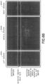
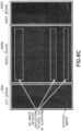
- Reflections detected in the middle region 600M but in the left region 600L and right region 600R for any given slot are mapped as being absent (e.g., an empty slot) (see Fig. 6C ).
- areas in the image corresponding to substrate holding slots in which a reflection in the middle region 600M exists but where there are no corresponding reflections in both the left region 600L and the right region 600R are mapped as being empty slots (i.e., substrate is absent).
- Fig. 13 illustrates the corrected true profile 500TC of the slot 13 substrate, which exhibits a warp/bow. Further, it is noted that the spatial correction can be applied prior to or after the processing the image by slicing of the image into the vertical image slices 410-416.
- the transport arm 180TA includes an end effector 180E movably mounted to the transport arm 180TA for loading substrates from the substrate carrier 110 through the opening 888 to the substrate processing apparatus 100, 150, 165 (and vice versa).
- each respective camera 210A, 210B, 210C is positioned with a field of view FOVA, FOVB, FOVC disposed to view, through the opening 888 with the common support 244 positioned by the transport arm 180TA at a common position CP, a different separate part of the substrate carrier 110 with wafer slots for holding at least one of the more one substrates S, separate and different from parts of the substrate carrier 110 with different wafer slots for holding substrates S different than the at least one substrate S viewed by each other camera 210A, 210B, 210C with the common support 244 at the common position CP, and each substrate S held in the substrate carrier 110 is imaged by the camera array 277 with the common support 244 at the common position CP.
- the at least one illuminator 220 is provided ( Fig. 14 , Block 1415) and is connected to the common support 244. As described above, the at least one illuminator is configured so as to illuminate, through the opening 888 with the common support 244 in the common position CP, an outer edge 233 of each substrate S in the substrate carrier 110, which edge delineates upper and lower edge boundaries 233U, 233L of the outer edge 233 of the substrate S.
- the at least one illuminator 220 is disposed with respect to each respective camera 210A, 210B, 210C, and the image of the corresponding separate different part (see, e.g., regions RA, RB, RC in Fig. 2C and the region of interest in Fig.
- each respective camera 210A, 210B, 210C is disposed so that the outer edge 233 directs reflected edge illumination, from the at least one illuminator 220, at the respective camera 210A, 210B, 210C, and optically blanks, at the upper edge boundary 233U and the lower edge boundary 233L, background reflection light, in the image captured of the separate different part of the substrate carrier 110 by the respective camera 210A, 210B, 210C through the opening 888 with the common support 244 at the common position CP.
- the outer edge 233 of the substrate S is defined with the upper and lower edge boundaries 233U, 233L in relief in image contrast, formed by and between the edge reflection and the optically blanked background, registered by each camera 210A, 210B, 210C so as to effect edge detection of each substrate S in the substrate carrier 110 with the common support 244 at the common position CP.
- the controller 199 commands movement of the transfer arm 180TA so that the transfer arm 180TA is positioned relative to the opening 888 ( Fig. 14 , Block 1420) for imaging the substrates S within the carrier 110 through the opening 888.
- the substrates S are illuminated by the at least one illuminator 220 and images of the substrates S in the different separate regions (see, e.g., regions RA, RB, RC in Fig. 2C ) are captured through the opening 888 by camera array 277 ( Fig. 14 , Block 1425).
- the controller 199 is configured to perform one or more of determining a substrate map and determining substrate warp/bow. As described herein, mapping and determining warps/bows of substrates may be determined in any suitable order relative to one another such as where both are desired to be determined.
- the controller 199 determines the intensity profile 480 (see Figs. 4A and 4B ) in the manner described herein ( Fig. 14 , Block 1430) for each of the different separate regions (e.g., regions RA, RB, RC). From the intensity profile 480, the controller 199 determines the true edge profile 500T in the manner described herein ( Fig. 14 , Block 1440) and the so as to determine the substrate map 280 ( Fig. 14 , Block 1442) for each different separate region and the substrate carrier 110 as a whole. The substrate state (e.g., absent, present, double, cross, shift) is determined ( Fig.
- Any substrate warping/bowing of the substrates in the different separate regions RA, RB, RC is determined by the controller 199 in any suitable manner (such as with the image processing described herein) from the corrected true edge profiles 500TC of the substrates S ( Fig. 14 , Block 1467).
- the warping/bowing determination is employed by the controller 199 to adjust the distance TD (or spacing) (see FIG. 1A ) between end effector tines 180ET1, 180ET2 for picking the warped/bowed substrates S ( Fig. 14 , Block 1470).
- a semiconductor wafer mapping apparatus comprises: a frame forming a wafer load opening communicating with a load station for a substrate carrier disposed to hold more than one wafers vertically distributed in the substrate carrier for loading through the wafer load opening; a movable arm movably mounted to the frame so as to move relative to the wafer load opening and having at least one end effector movably mounted to the movable arm to load wafers from the substrate carrier through the wafer load opening; an image acquisition system including an array of cameras arranged on a common support and each camera is fixed with respect to the common support that is static with respect to each camera of the array of cameras, wherein each respective camera is positioned with a field of view disposed to view, through the wafer load opening with the common support positioned by the movable arm at a common position, a different separate part of the substrate carrier with wafer slots for holding at least one of the more one wafers, separate and different from parts of the substrate carrier with different wafer slots for holding wafer
- each different separate part viewed by the respective camera of the array of cameras has a different set of wafer slots, corresponding to the separate part and the respective camera, vertically distributed at predetermined reference heights viewed by the respective camera.
- the semiconductor wafer mapping apparatus further comprises a controller communicably coupled to the movable arm to move the movable arm relative to the frame and position the common support at the common position.
- a semiconductor wafer mapping apparatus comprises: a frame forming a wafer load opening communicating with a load station for a substrate carrier disposed to hold more than one wafers vertically distributed in the substrate carrier for loading through the wafer load opening; a movable arm movably mounted to the frame so as to move relative to the wafer load opening and having at least one end effector movably mounted to the movable arm to load wafers from the substrate carrier through the wafer load opening; an image acquisition system including an array of cameras arranged on a common support and each camera is fixed with respect to the common support that is static with respect to each camera of the array of cameras, wherein each respective camera is positioned with a field of view disposed to view, through the wafer load opening with the common support positioned by the movable arm at a common position, a corresponding different separate part of the substrate carrier each with at least one corresponding wafer slot different from at least one other wafer slot in each other corresponding different separate part of the substrate carrier, each
- each of the corresponding different separate part is imaged by but one respective camera of the array.
- each of at least one wafer held in the corresponding wafer slot of the corresponding different separate part is imaged by but one of the respective camera of the array of cameras.
- the semiconductor wafer mapping apparatus further comprises a controller communicably coupled to the array of cameras and programmed with each respective camera calibration, that has a baseline image for the respective camera, different from the baseline image of each other respective camera, the baseline image defining predetermined baseline characteristics for each of at least one wafer in each of the at least one corresponding slot of the corresponding separate different part imaged by the respective camera.
- the illumination source is dispose relative to the respective camera so that reflected light from planar surfaces of the wafer and each other wafer slotted in the substrate carrier are optically blanked in each image by the respective camera of the different separate part of the substrate carrier.
Landscapes
- Engineering & Computer Science (AREA)
- Computer Vision & Pattern Recognition (AREA)
- Physics & Mathematics (AREA)
- General Physics & Mathematics (AREA)
- Theoretical Computer Science (AREA)
- Container, Conveyance, Adherence, Positioning, Of Wafer (AREA)
Description
- This application is a non-provisional of and claims the benefit of
United States provisional patent application number 63/046,555, filed June 30, 2020 - The exemplary embodiments generally relate to semiconductor fabrication equipment, and more particularly, to identification of substrate in semiconductor fabrication equipment.
- There are various places that a single substrate or a stack of substrates (such as, e.g., wafers, reticles, filmframes, trays, etc.) can be held in semiconductor fabrication equipment. The physical state of the substrate at each of these locations can be one of many, including but not limited to, absent, present, double-slotted, cross-slotted, and shifted/tilted. Generally, the physical state of each substrate at the holding locations is determined (or mapped) to facilitate substrate handling within the semiconductor fabrication equipment.
- One example of substrate mapping of a single substrate, such as located on a robotic end effector, includes a vacuum-suction technique where a vacuum suction cup is in contact with the back side of the substrate. By opening a valve on a vacuum line of the end effector, the vacuum pressure level of the suction cup determines the substrate state, which in this case is present or absent (the vacuum-suction technique does not detect substrate shifting). The vacuum-suction technique may result in a false reading when the contact of the substrate with the vacuum suction cup is not tightly sealed. In addition, it takes a few hundred milliseconds of time between activation of the vacuum valve and establishing a steady state vacuum pressure level to obtain a determination of the presence or absence of the substrate on the end effector. As may be realized, a few hundred milliseconds over a number of wafers has a negative impact on substrate throughput through the semiconductor fabrication equipment.
- Generally, for mapping a stack of substrates (with gaps separating each of the stacked substrates) held at, for example, a load port in a substrate cassette or carrier, a break-beam technique is employed. Here a light beam extends from a transmitter to a receiver in a direction parallel to the substrate planes. The transmitter and receiver may be referred to as a through-beam sensor. The through-beam sensor is moved up or down along a side of the substrate stack so that the light beam engages and is broken by the substrates (a break in the light beam indicates a presence of a substrate). While the break-beam technique can detect many of the substrate states noted above, the break-beam technique is sensitive to the angle of the light beam relative to the substrate planes such that it is desired the light beam be precision aligned with the substrate planes. Here, extending and retracting the through-beam sensor to and from the substrate holding location takes at least a few seconds and the correlation of beam breaking and beam restoring events for each substrate position generally entails a controlled and slow motion profile of the through-beam sensor, all of which negatively impact substrate throughput.
- Both the vacuum-suction and break-beam techniques involve complexity in mechanical design. For example, the vacuum-suction technique employs a vacuum supply to the substrate handling equipment, and involves routing a vacuum line through a substrate transport arm to the end effector. The break-beam technique involves moving parts as well as extension and retraction of the through-beam sensor. This increased complexity increases the costs of manufacturing and servicing the semiconductor processing equipment.
- In addition to the above, in advanced semiconductor fabrication technology the substrates are provided with varied thicknesses. The different thicknesses of the substrates pose a challenge to the break-beam technique in determining the map of the substrate holding location. For example, thin substrates may have a thickness that does not completely block the light beam resulting in a false identification of an absent substrate.
- Imaging systems have also been employed for substrate mapping; however, in conventional image mapping systems substrates, such as those imaging substrates through a load port opening, images of substrates towards the top (or bottom) of the substrate stack may be distorted or some substrates may be blocked from view by substrates positioned above or below. There may also be an issue with light reflecting off of the substrates and/or an interior of the substrate carrier which reflected light may obscure substrate detection.
- Further, in semiconductor fabrication facilities, various types of substrates (as noted above) are transported by substrate transports (e.g., robots) having end effectors on which the substrates are seated for transport. To transport a substrate, the substrate transport extends the end effector into a small space below (or from above for some applications) the substrate (e.g., seated on a substrate seating surface of a substrate carrier, process module, or other suitable substrate holding location) to pick up the substrate. Picking the substrate with the end effector poses no issues where the substrate is flat; however, as noted above, in advanced semiconductor fabrication technology the substrates are provided with varied thicknesses and may not be flat. For example, thinned substrates, reconstructed substrates, and fan-out substrates in advanced packaging may bow/warp up to a few millimeters. The warping of these substrates may prevent an end effector from extending into the small space below (or above) the substrate to pick the substrate up.
- The following document is cited as being a pertinent prior art illustration:
US 2005/086024 A1 discloses a semiconductor wafer mapping apparatus. - The following additional documents are also mentioned as a complementary prior art illustration:
- The foregoing aspects and other features of the disclosed embodiment are explained in the following description, taken in connection with the accompanying drawings, wherein:
-
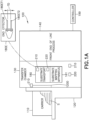
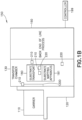
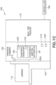
Figs. 1A ,1B , and1C are exemplary substrate processing apparatus incorporating aspects of the present disclosure; -
Figs. 2A ,2B, and 2C are exemplary schematic illustrations of a machine vision system and illuminator(s) of the substrate processing apparatus ofFigs. 1A ,1B , and1C in accordance with aspects of the present disclosure; -
Figs. 3A ,3B, 3C, and 3D are exemplary schematic illustrations of portions of the machine vision system and illuminator(s) ofFigs. 2A ,2B, and 2C in accordance with aspects of the present disclosure; -
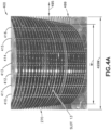
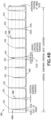
Fig. 4A is an exemplary image of substrates captured by the machine vision system ofFigs. 2A ,2B, and 2C in accordance with aspects of the present disclosure; -
Fig. 4B is an exemplary intensity profile of the image ofFig. 4A in accordance with aspects of the present disclosure; -
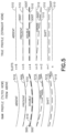
Fig. 5 is an exemplary comparison of a raw profile of imaged substrates imaged by the machine vision system ofFigs. 2A ,2B, and 2C and corresponding true profiles of the imaged substrates in accordance with aspects of the present disclosure; -
Fig. 6A is an exemplary image of a stack of substrates with upper and lower edges boundaries of the substrates and background optically blanked in accordance with aspects of the present disclosure; -
Figs. 6B and6C are exemplary images of substrates in a stack of substrates in accordance with aspects of the present disclosure; -
Fig. 6D is an example of image optimization showing an optimization of an image of a stack of substrates so as to isolate edges from a background of the image in accordance with aspects of the present disclosure; -
Fig. 6E is an example of the isolates edges ofFig. 6D in a region of interest in accordance with aspects of the present disclosure; -
Fig. 6F is an example of image optimization where the isolates edges ofFig. 6D within a common substrate holding slot of a carrier being connected and present with boundaries of the respective substrate holding slots in accordance with aspects of the present disclosure; -
Fig. 7A is an exemplary illustration of the illuminator(s) ofFigs. 2A ,2B, and 2C in accordance with aspects of the present disclosure; -
Fig. 7B is a schematic illustration of an exemplary light path of one or more of the illuminator(s) ofFig. 7A in accordance with aspects of the present disclosure; -
Fig. 8A is a schematic illustration of an exemplary transport arm of the substrate processing apparatus ofFigs. 1A ,1B , and1C in accordance with aspects of the present disclosure; -
Fig. 8B is a schematic illustration of an exemplary light path of one or more of the illuminator(s) of of the transport arm ofFig. 8A in accordance with aspects of the present disclosure; -
Figs. 9A, 9B ,9C, and 9D are exemplary schematic illustrations of raw edge profiles and true profiles of substrates imaged from different angles in accordance with aspects of the present disclosure; -
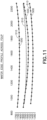
Figs. 10 ,11 ,12, and 13 are exemplary illustrations of raw edge profiles and corrected true profiles in accordance with aspects of the present disclosure; -
Fig. 14 is an exemplary flow diagram of a method in accordance with aspects of the present disclosure; -
Figs. 15A, 15B, 15C, and 15D illustrate exemplary baseline images of a substrate carrier in accordance with aspects of the present disclosure; and -
Figs. 16A and 16B are schematic illustrations of raw and true profile images of substrates taken by multiple cameras each capturing an image of a respective different separate region of a substrate carrier in accordance with aspects of the present disclosure. -
Figs. 1A ,1B , and1C illustrate exemplarysubstrate processing apparatus - Referring to
Figs. 1A ,1B ,1C , and2A , the aspects of the present disclosure provide a substrate mapping apparatus 181 (also referred to herein as a semiconductor wafer mapping apparatus) that includes a machine vision system 200 (also referred to herein as an image acquisition system) and at least one illuminator 220 (e.g., distributed direct or indirect light source including, but not limited to, LEDs, fluorescent light, flood light, light arrays, etc., or a combination thereof) for performing substrate mapping and/or substrate edge profiling. In accordance with the aspects of the present disclosure themachine vision system 200 includes at least one camera 210 (or any suitable image acquisition sensor). The at least onecamera 210 of themachine vision system 200 and the at least oneilluminator 220 are placed at one or more positions to capture images of asubstrate stack 270 disposed at any suitable location of thesubstrate processing apparatus camera 210 is a camera array 277 (also referred to herein as a camera system or array of cameras) as described herein. A substrate map 280 (referred to herein as a map) of the substrates S (also referred to herein as wafers) in thesubstrate stack 270 is determined from, for example,true edge profiles 500T (seeFig. 5 ) (or in some aspects corrected true edge profiles 500TC as shown in, e.g.,Fig. 10 ) of substrates S in thesubstrate stack 270 through any suitable analyzation/processing of the captured images of the substrates S in thesubstrate stack 270. As may be realized from the present disclosure, thesubstrate mapping apparatus 181 disclosed herein overcomes the deficiencies, such as those noted above, of conventional substrate mappers. Thesubstrate mapping apparatus 181 of the present disclosure is substantially free of moving parts and can be integrated into any suitable semiconductor fabrication equipment (also referred to herein as substrate processing apparatus), such assubstrate processing apparatus - The aspects of the present disclosure also provide for measuring edge profiles of the substrates S so that a distance TD (see
Fig. 1A ) between substrate holding tines 180ET1, 180ET2 of anend effector 180E (see alsoFig. 8A ) of a substrate transport 180 (SeeFig. 1A ) can be adjusted to pick up warped/bowed substrates. Suitable examples of end effectors having adjustable tines can be found inUnited States patent application number 15/693,871 filed on September 1, 2017 - Suitable examples of a
substrate transport 180 in which the end effectors with adjustable substrate holding tines 180ET1, 180ET2 can be incorporated is described inUnited States patent application number 14/928,352 filed on October 30, 2015 - As will be described herein, the at least one
camera 210 and the at least oneilluminator 220 are disposed at positions that capture images of the substrate S or thesubstrate stack 270 across a width of the substrate(s) S. The edge profile of each substrate S is defined from processing the captured images. Based on the edge profiles of the substrate(s), the available space below each substrate S across its width is determined in any suitable manner. Thesubstrate transport 180 under control of any suitable controller, such ascontroller 199, commands adjustment of a distance TD (seeFIG. 1A ) between substrate holding tines 180TE1, 180TE2 of theend effector 180E so that the tines extend into regions underneath the warped/bowed substrate S having clearance that allows theend effector 180E to extend under the substrate S. - Generally, as described in greater detail herein, the aspects of the present disclosure employ the at least one
camera 210 to capture images ofouter edges 233 of substrates while the substrates are illuminated by the at least oneilluminator 220. Here, any suitable controller (such as controller 199) defines the substrate edge profiles from the captured image(s) using any suitable algorithms such as those described herein. A number of data points on theouter edge 233 of each substrate imaged by the at least onecamera 210 is maximized through the employment of distributed and diffused illumination across the substrate width W where multiple exposure techniques (e.g., adjusting exposure speed, aperture, etc.) for different sections of the substrate width are employed. The accuracy of the data points on theouter edge 233 of each substrates S is maximized by an algorithm (e.g., which is programmed into the controller 199) that captures and stores the edge profiles of a standard substrate as spatial calibration data 281 (as will be described in greater detail herein). At runtime of thesubstrate mapping apparatus 181 for determining themap 280 and/or edge profiles, the measured substrate raw profiles are compared against thespatial calibration data 281 to determine corrected true profiles 500TC of the substrates S (SeeFigs. 10-13 ). The raw profile is the edge profile of a substrate as seen by a respective camera (i.e., the projection of the three-dimensional substrate edge onto the two-dimensional plane of the camera's field of view - see the left-hand side inFig. 5 and alsoFigs. 9B-9D ). Thetrue profile 500T and/or corrected true profile 500TC is what anend effector 180E of asubstrate transport 180 would "see" when picking a substrate S (i.e., a straight-on projection of the three-dimensional substrate edge onto the plane of extension/retraction of theend effector 180E - see the right-hand side ofFig. 5 and alsoFig. 9A ). - Referring to
Figs. 1A ,1B , and1C , the aspects of the present disclosure will be described with respect tosubstrate processing apparatus multiple carriers 110 are coupled to atransfer chamber 130 and substrates are moved from onecarrier 110 to anothercarrier 110 by asubstrate transport 180 within the transfer chamber 130 (e.g., to arrange the substrates in one or more carriers according to a predetermined sequence/order), where there is no substrate process (such asprocess Fig. 1A , thesubstrate processing apparatus 100 includes aload port 120, atransport chamber 130, and any suitable front end of line process 140 (e.g., generally including thin film processes that use vacuum such as etching, chemical vapor deposition, plasma vapor deposition, implantation, metrology, rapid thermal processing, dry strip atomic layer, oxidation/diffusion, forming of nitrides, lithography, epitaxy, or other thin film processes for fabrication of individual semiconductor structures patterned in the semiconductor up to, but not including, the deposition of metal interconnect layers). Theload port 120 is coupled to atransport chamber 130 and is configured to interface any suitable substrate cassette orcarrier 110 to thetransport chamber 130. Thetransport chamber 130 is coupled to the front end ofline process 140 and includes any suitable opening and/or valves through which substrates are passed between thetransport chamber 130 and the front end ofline process 140. - The
transport chamber 130 includessubstrate transport 180 configured to transfer substrates S between thesubstrate carrier 110 and the front end ofline process 140. Here thesubstrate transport 180 includes the transport arm 180TA having anend effector 180E for loading and unloading substrates S to and from thesubstrate carrier 110 through anopening 888 of theload port 120. As noted above, a suitable example of asubstrate transport 180 can be found inUnited States patent application number 14/928,352 filed on October 30, 2015 - For example, referring also to
Figs. 8A and8B , the aspects of the disclosed embodiment will be described with respect to anatmospheric transport robot 180 but it should be understood that the aspects of the disclosed embodiment are equally applicable to vacuum transport robots such as those found in the front end ofline process 140, the back end ofline process 160, and theback end process 170. As may be realized, thesubstrate transport 180 is mounted to alinear slide 850 or a boom arm BA (such as described inUnited States patent application number 14/377,987 filed on August 11, 2014 - As can be seen in
Figs. 1A-1C and8A , in one aspect, thesubstrate transport 180 is movably mounted to aframe 800 of thetransport chamber 130 or in other aspects to a frame of any suitable module of thesubstrate processing apparatus frame 800 includes one or more openings 888 (also referred to herein as a wafer load opening) communicating with the load port 120 (also referred to herein as a load station) for thesubstrate carrier 110 that is disposed on theload port 120 to hold one or more than one substrate S in a vertically distributed arrangement (as described herein) for loading into the substrate processing apparatus 100 (and similarly into thesubstrate processing apparatus opening 888. Thesubstrate transport 180 includes a transport arm 180TA (also referred to herein as a movable arm) that, in one aspect, is mounted to acarriage 863 so that the transport arm 180TA is movably mounted to theframe 800. Thecarriage 863 is, in one aspect, mounted to thelinear slide 850 so as to be movable in the X direction while in other aspects thecarriage 863 is mounted to theframe 800 so as to be fixed in the X (and/or Y direction). In one aspect anysuitable drive 867 is mounted to theframe 800 and drivingly connected to thecarriage 863 by any suitable transmission for moving the transport arm 180TA in the X direction. In this aspect the transmission is a belt and pulley transmission and the drive is a rotary drive but in other aspects thedrive 867 is a linear actuator that is drivingly connected to thecarriage 863 with any suitable transmission or without a transmission (e.g. such as where the carriage includes a drive portion of the linear actuator). Here the transport arm 180TA includes arotational drive 862, a Z-drive column 830, aslide body 820 and one ormore end effectors 180E. Therotational drive 862 is any suitable rotational drive mounted to thecarriage 863 and theZ drive column 830 is mounted to an output of therotational drive 862 so as to rotate in the direction of arrow T about the θ axis (e.g. the θ direction). Theslide body 820 is movably mounted to theZ drive column 830 where the Z-drive column 830 includes any suitable drive motor and/or transmission for moving theslide body 820 in the Z direction. - The one or more (e.g. at least one)
end effectors 180E are movably mounted to theslide body 820 in any suitable manner so as to extend and retract in the R direction (noting the R direction rotates about axis θ so that extension of the end effector(s) 180E can be aligned with the X or Y axes or at any suitable rotational angle in the X-Y plane). While twoend effectors 180E are illustrated for exemplary purposes only it should be understood that any suitable number of end effectors are mounted to theslide body 820. As may be realized, the one ormore end effectors 180E traverse, with the transport arm 180TA as a unit, in a first direction (e.g. one or more of the X, Y and Z directions) relative to theframe 800 and traverses linearly, relative to the transport arm 180TA, in a second direction (e.g. the R direction) that is different from the first direction. Theslide body 820 includes one or morelinear drives 825 configured to independently move eachend effector 180E in the R direction. The one or morelinear drives 825 are any suitable drive(s) having any suitable transmissions which in one aspect are substantially similar to those described in, for example,United States provisional patent application number 61/917,056 filed on December 17, 2013 - The
end effectors 180E are arranged on theslide body 820 so that they are stacked one over the other so as to have a common axis R of extension and retraction. The end effectors may also include any suitable drives for adjusting the distance TD (seeFIG. 1A ) between the end effector tines 180ET1, 180ET2 as described inUnited States patent application number 15/693,871 filed on September 1, 2017 - The
carrier 110 may be anysuitable carrier 110 such as a front opening carrier (illustrated inFigs. 1A and1B - a suitable example of which is a front opening unified pod (FOUP)) or bottom opening carrier (a suitable example of which is a standard mechanical interface (SMIF) pod). In one aspect, thecarrier 110 may be substantially similar to those described inUnited States patent number 9,105,673 issued on August 11, 2015 - In one aspect, the
transport chamber 130 has the same atmosphere (e.g., a vacuum atmosphere) as that of the front end ofline process 140; while in other aspects the transport chamber has an atmospheric environment and the front end ofline process 140 includes any suitable load lock for transferring substrates S between the front end ofline process 140 and thetransport chamber 130 without degradation of a processing atmosphere of the front end ofline process 140. - Referring to
Fig. 1B , thesubstrate processing apparatus 150 includes the load port 120 (similar to that described herein), the transport chamber 130 (similar to that described herein), and any suitable back end of line process 160 (e.g., generally associated with fabrication of metal interconnect layers of the semiconductor structures formed by the front end ofline process 140 and includes any suitable processing steps after the front end of line process up to and including final passivation layer fabrication). Theload port 120 is coupled to atransport chamber 130 and is configured to interface anysuitable substrate carrier 110 to thetransport chamber 130. Thetransport chamber 130 is coupled to the back end ofline process 160 and includes any suitable opening and/or valves through which substrates are passed between thetransport chamber 130 and the back end ofline process 160. Thetransport chamber 130 includes substrate transport 180 (such as that described above) configured to transfer substrates between thecarrier 110 and the back end ofline process 160. Thecarrier 110 may be anysuitable carrier 110 such as a front opening carrier (illustrated inFigs. 1A and1B - a suitable example of which is a front opening unified pod (FOUP)) or bottom opening carrier (a suitable example of which is a standard mechanical interface (SMIF) pod). In one aspect, thecarrier 110 may be substantially similar to those described inUnited States patent number 9,105,673 issued on August 11, 2015 - In one aspect, the
transport chamber 130 has the same atmosphere (e.g., a vacuum atmosphere) as that of the back end ofline process 160; while in other aspects the transport chamber has an atmospheric environment and the back end ofline process 160 includes any suitable load lock for transferring substrates S between the back end ofline process 160 and thetransport chamber 130 without degradation of a processing atmosphere of the back end ofline process 160. - Referring to
Fig. 1C , thesubstrate processing apparatus 165 includes the load port 120 (similar to that described herein), the transport chamber 130 (similar to that described herein), and any suitable back end process 170 (e.g., generally including substrate test, substrate backgrinding, die separation, die tests, IC (integrated circuit) packaging, and final test). Theload port 120 is coupled to atransport chamber 130 and is configured to interface anysuitable substrate carrier 110 to thetransport chamber 130. Thetransport chamber 130 is coupled to theback end process 170 and includes any suitable opening and/or valves through which substrates S are passed between thetransport chamber 130 and theback end process 170. Thetransport chamber 130 includes substrate transport 180 (such as that described above) configured to transfer substrates between thecarrier 110 and theback end process 170. Thecarrier 110 may be anysuitable carrier 110 such as a front opening carrier (illustrated inFigs. 1A and1B - a suitable example of which is a front opening unified pod (FOUP)) or bottom opening carrier (a suitable example of which is a standard mechanical interface (SMIF) pod) as noted above. In one aspect, thecarrier 110 may be substantially similar to those described inUnited States patent number 9,105,673 issued on August 11, 2015 - Referring to
Figs. 2A ,2B and 2C , thesubstrate mapping apparatus 181 will be described with respect to one substrate S or a stack ofsubstrates 270 held in asubstrate carrier 110 seated on and engaged with theload port 120; however, in other aspects the one substrate S or stack ofsubstrates 270 may be disposed at any suitable location of thesubstrate processing apparatus substrate mapping apparatus 181 includes at least onecamera 210 and at least oneilluminator 220 that are coupled to any suitable controller, such ascontroller 199 thesubstrate processing apparatus substrates 270 is/are illuminated by the at least oneilluminator 220 as will be described herein so that the at least one camera captures at least one image of the substrate edge(s) illuminated by the at least oneilluminator 220. Signals embodying the image are transmitted from the at least onecamera 210 to thecontroller 199 for processing of the image and to extract (or otherwise determine) themap 280 from the image using any suitable image processing algorithms. Themap 280 is stored in anysuitable memory 199M of or accessible by thecontroller 199 so that thecontroller 199 can command movement of substrate transport equipment based on a state of the substrate S or each substrate in thesubstrate stack 270 as determined by themap 280. As will be described herein, in one or more aspects a single camera and illuminator pair is employed to image the substrate(s) S and determine the map, while in other aspects more than one camera and/or more than one illuminator are used. In some aspects, such as depending on a substrate type (e.g., thickness, shape, material, etc.) as well as an environment surrounding the substrate (e.g., located within acarrier 110, located within an unenclosed rack, etc.), more than one image of the substrate S orsubstrate stack 270 are taken and analyzed as described herein to determine themap 280. For exemplary purposes only, the description provided herein assumes only a single image is analyzed; however, as noted above more than one image can be compared, superposed, etc. and analyzed in a manner similar to that described herein without departing from the aspects of the present invention which is defined by the appended claims. - Also for ease of explanation, the present disclosure is described with respect to analyzation of
substrate stack 270; however, analyzation of a single substrate S is substantially similar to that described herein. - As will be described herein, the
map 280 is determined or otherwise generated to determine the state of each substrate S in each holding slot of thesubstrate stack 270. An image of thesubstrate stack 270 is taken with the at least onecamera 210 and at least oneilluminator 220 in any suitable location(s) relative to thesubstrate stack 270 so thatouter edges 233 of the substrates S in thesubstrate stack 270 are captured in the image (see, e.g.,image 400 inFig. 4 ). The image is processed by thecontroller 199 in any suitable manner, such as described herein, to identify theouter edges 233 of the substrates S, where at least a partial definition of theouter edge 233 is performed by thecontroller 199 based on the image. - As noted briefly above, and referring also to
Fig. 5 , for each holding slot of the substrate stack 270 (noting that the holding slot(s) (n, n+1, n+2, ...; each having a predetermined height relative to a load port reference location as provided for in SEMI® standards) is/are defined by thesubstrate carrier 110 or other substrate support and are arranged to support a respective substrate S in thesubstrate stack 270 with a predetermined distance or pitch between the substrates S) the edge data of each substrate S (see, e.g.,Fig. 5 ) is determinative of the state of the substrate S in the holding slot based on the following exemplary substrate mapping rules: - where no substrate edge 500 (the
substrate edge 500 in the image being theouter edge 233 of the substrate S in the stack of substrates 270) is detected in the image the state of the substrate S for any given holding slot is absent (i.e., no substrate is present); - where a
single substrate edge 500 is detected in the image or a shape line (indicative of a substrate edge 500) is detected in the image as overlapping with a holdingslot baseline 510 the state of the substrate S in any given holding slot is present (i.e., a single substrate is present in the holding slot); - where two
substrate edges 500 are detected in the image or a thickness of the substrate S detected in the image is, for example, twice (or any suitable multiple of) an expected substrate thickness, the state of the substrate S in any given holding slot is double (i.e., two substrates S are disposed one on top of the other in the same holding slot); - where a shape line (indicative of a substrate edge 500) is not parallel to a
baseline 510 of the holding slot the state of the substrate S in any given holding slot is cross (i.e., cross-slotted where one substrate is placed across two slots, such as slots n+2 and n+3 inFig. 5 ); - where a shape line (indicative of a substrate edge 500) is parallel to a
slot baseline 510 but shifted vertically (such parallelism being detectable when the at least onecamera 210 views the substrate S from an angle (i.e., from above or below the substrate S) the state of the substrate S in any given holding slot is shifted or tilted (i.e., the substrate has slid out of its nominal position within the holding slot). - Referring to
Figs. 2A ,2B ,2C and3A , in accordance with aspects of the present disclosure, the at least onecamera 210 is mounted in one or more of anear plane 300 and afar plane 301. Thenear plane 300 is adjacent the substrate carrier 110 (e.g., seated on the load port 120) while thefar plane 301 is further away from thesubstrate carrier 110. Thenear plane 300 is any suitable distance Y1 that is nearest theopening 399 of thesubstrate carrier 110 with all of the substrates S stacked within thesubstrate carrier 110 captured in and substantially fill a field of view FOVW of thecamera 210 fitted with the wide angle lens (seeFig. 3C ). Thefar plane 301 is any suitable distance Y2 that is nearest theopening 399 of thesubstrate carrier 110 with all of the substrates S stacked within thesubstrate carrier 110 captured in and substantially fill a field of view FOVT of thecamera 210 fitted with a telephoto lens (Fig. 3D ). As may be realized, the distances Y1, Y2 can be determined based on a height of thesubstrate stack 270 and a focal length of the respective wide angle lens and telephoto lens. In accordance with the present disclosure, the mounting location of the at least onecamera 210 in the X direction is substantially along a vertical (Z-axis) centerline 371 of the substrate stack 270 (not shown inFig. 3A for clarity but is substantially coincident with a vertical centerline of the substrate carrier 110); however, in other aspects the at least onecamera 210 can be mounted on one or more sides (e.g., to the left or right) of thevertical centerline 371. The mounting location of the at least onecamera 210 in the Z direction may be substantially in-line with a horizontal center plane 370 (the X-Y plane) of thesubstrate carrier 110; however, in other aspects the at least onecamera 210 can be mounted above or below thecenter plane 370.Fig. 2B illustrates asingle camera 210 mounted in-line with thehorizontal center plane 370 whileFig. 2C illustrates acamera 210B mounted at thehorizontal center plane 370, acamera 210A mounted above thehorizontal center plane 370, and acamera 210C mounted below the horizontal center plane 370 (noting thatFigs. 2B and 2C are generic with respect tonear plane 300 and far plane 301). In other aspects more or fewer cameras may be used. The one or more cameras described herein are generally referred to as at least one camera 210 (which is inclusive of a single camera or a system/array ofcameras - In one or more aspects, at least one of the at least one
camera 210 is mounted at the lower center location LC so as to image thesubstrate stack 270 in an angled upwards direction. In lower center location LC the resulting image substantially eliminates background noise due to, for example, environmental reflections (such as from the interior of the carrier 110) and/or top surfaces of the substrates which may include the die grip patterns. Here the substrates are illuminated from one or more of the locations (e.g., upper left UL, upper center UC, upper right UR, middle left ML, middle center MC, middle right MR, lower left LL, lower center LC, and lower right LR). In one or more aspects, at least one of the at least onecamera 210 is mounted at the upper center location UC where the substrate stack is illuminated from one or more of the lower locations LL, LC, LR and middle locations ML, MC, MR so that at least background noise from or imaging of the top surface of the substrate is suppressed (e.g., the top surfaces of the substrate are cast in shadow in a manner similar to that described inUnited States patent application number 16/570,453 filed on September 13, 2019 - In one or more aspects, at least one of the at least one
camera 210 is mounted at the middle center location MC where thesubstrate stack 270 is illuminated from one or more of the lower locations LL, LC, LR to suppress at least background noise from or imaging of the top surface of the substrates S. In still other aspects, the at least onecamera 210 may be located at any number and combination (such as where the at least onecamera 210 comprises more than one camera) of the mounting locations UL, US, UR, ML, MC, MR, LL, LC, LR on thenear plane 300 and/orfar plane 301; however, where the at least onecamera 210 is mounted at the middle center location MC on thenear plane 300 the at least onecamera 210 is mounted to a load port door 120D of the load port so that the at least one camera is moved with the load port door from a substrate transfer path to and from thesubstrate cassette 110. Here, the at least onecamera 210 images the substrate stack 270 (with one or more images) as the load port door 120D moves to open and close the load port/substrate carrier. - Referring to
Figs. 1A-1C and2C , the at least onecamera 210 is mounted to a fixed location within an interior of thesubstrate processing apparatus Figs. 1A-1C ). The at least onecamera 210 can also be mounted to a movable component (e.g., the load port door 120D and/or substrate transport 180) of thesubstrate processing apparatus Figs. 1A-1C ). Here the movable component positions the at least onecamera 210 in the desired location UL, US, UR, ML, MC, MR, LL, LC, LR on thenear plane 300 and/orfar plane 301 for imaging thesubstrate stack 270.Fig. 2C illustrates an example, where thecamera array 277 including more than onecamera substrate transport 180. Here, thecamera array 277 is located on a common support 244 (which in this aspect is the Z-drive column 830) of the substrate transport 180 (where the "common support" refers to a single support to which each camera in thecamera array 277 is mounted so that the cameras share the single support); however, in other aspects, where stationarily mounted in thetransfer chamber 130 thecamera array 277 may be mounted to any common support of thesubstrate processing apparatus substrate processing apparatus camera common support 244. Thecommon support 244 is static with respect to eachcamera cameras - In one aspect, any
suitable camera controllers 278 are located on thesubstrate transport 180 and are coordinated by any suitable controller, such ascontroller 199; while, in other aspects thecamera controllers 278 are incorporated intocontroller 199. In one or more aspects, the at least oneilluminator 220 is mounted to thesubstrate transport 180 or in a stationary location within thesubstrate processing apparatus - Where the at least one
camera 210 and, in some aspects, the at least oneilluminator 220 is/are mounted to thesubstrate transport 180, thesubstrate transport 180 transports the at least a portion of themachine vision system 200 to any desired location within thesubstrate processing apparatus substrate stack 270 is held. Mounting the at least onecamera 210 and, in some aspects, the at least oneilluminator 220 to thesubstrate transport 180 may decrease the number of cameras and illuminators (such as where thesubstrate processing apparatus substrate carriers 110 are held andsubstrate stacks 270 are mapped) and may provide for optimal positioning (e.g., unobstructed fields of view on thenear plane 300 and/orfar plane 301 at any one or more of the locations UL, US, UR, ML, MC, MR, LL, LC, LR) of the at least onecamera 210 and at least oneilluminator 220 regardless of the construction of the robotic environment (i.e., the interior of thesubstrate processing apparatus - In the example illustrated in
Fig. 2C (see alsoFigs. 8A and8B ), eachrespective camera drive column 830 of thesubstrate transport 180 so that the fields of view FOVA, FOVB, FOVC extend in a direction parallel to or along thecenter plane 370 of the substrate carrier 110 (e.g., perpendicular to an extension axis of the substrate transport end effector). Here the fields of view FOVA, FOVB, FOVC are positioned on the Z-drive column 830 (i.e., the common support 244) to view, through theopening 888 with the Z-drive column 830 positioned by the transfer arm 180TA (Fig. 8A ) at a common position CP (seeFig. 8B - where the "common position" refers to a single position of the substrate transport so that thecameras common support 244 are dependent from the single position of the common support 244) relative to theopening 888, a different separate part (see, e.g., regions RA, RB, RC inFig. 2C , and a representative region of interest (i.e., any one of the regions RA, RB, RC) inFig. 6E ) of thesubstrate carrier 110. Each different separate region RA, RB, RC has substrate slots for holding at least one or more than one substrates S, separate and different from parts of thesubstrate carrier 110 with different substrate holding slots for holding substrates S different than the at least one or more than one substrates S in regions/parts viewed by eachother camera axis drive 830 at the common position CP. Each substrate S held in thesubstrate carrier 110 is imaged bycamera array 277 with the Z-axis drive 830 at the common position CP. In some aspects, each of the corresponding different separate parts is imaged by but onerespective camera respective camera respective camera respective camera controller 199 is communicably coupled to the transport arm 180TA to move the transport arm 180TA relative to the frame 800 (seeFig. 8 ) and position thecommon support 244 at the common position CP. - Each different separate part of the
substrate carrier 110 andsubstrate stack 270 therein viewed by therespective camera camera array 277, has a different set of wafer slots, corresponding to the separate part and therespective camera respective camera load port 120 on which thesubstrate carrier 110 is seated. For example, each field of view FOVA, FOVB, FOVC of therespective camera substrate stack 270 therein). In one or more aspects, an image captured by eachrespective camera respective camera substrate carrier 110 is imaged by thecamera array 277 with thecommon support 244 at the common position CP. In this example, thesubstrate carrier 110 is a 25 substrate carrier and region of interest RC corresponds to holding slots 1-8, region of interest RB corresponds to holding slots 9-17, and region of interest RA corresponds to holding slots 18-25. The fields of view FOVA, FOVB, FOVC may overlap any desired amount to provide substantially complete coverage of the interior 222 (which in some aspects may increase the amount of image information and increase resolution of the resulting map 280); while in other aspects, as described herein, the fields of view may not overlap or be cropped for image processing. In this aspect, image processing is performed as described herein for each image captured byrespective camera controller 199 combines the respective processed images to generate themap 280 of thesubstrate stack 270 within thesubstrate carrier 110. - While the
cameras Fig. 2C are illustrated one above the other (e.g., in locations UC, MC, LC) in other aspects, (which also apply to stationarily mounted cameras) may be mounted in any number of the locations UL, US, UR, ML, MC, MR, LL, LC, LR so as to form one dimensional vertical (in the Z direction) camera arrays, one dimensional horizontal (e.g., in the X direction) camera arrays, or a two dimensional arrays of cameras (e.g., in the X-Z plane). As may be realized, generally for round shaped substrates, the far left side FL and far right side FR (seeFig. 2A ) of the substrates when viewed through theopening 888 may be dimmer in illumination as the substrateouter edge 233 curves away from the at least onecamera 210. Where the edge signal obtained by the at least onecamera 210 falls below any suitable predetermined threshold, additional images of the substrates can be taken with longer exposure times and/or with a larger camera aperture. As may be realized, the longer exposure times and/or larger aperture may cause overexposure of a center region WC of the substrate in the image, where several images (low exposure and high exposure images) are combined using any suitable image processing algorithms including, but not limited to, high dynamic range (HDR) algorithms, or combining different vertical segments of the different images to produce a resulting image that has a uniform exposure that highlights the substrate edges 233. As such, cameras located in different ones of the locations UL, US, UR, ML, MC, MR, LL, LC, LR may be programmed with different aperture sizes and or exposure speeds that are optimized for different regions of the substrate stack/substrate carrier. For example, cameras closer to the at least oneilluminator 220 may have a slower exposure speed and/or smaller aperture than cameras further from the at least oneilluminator 220 so as to substantially prevent overexposure of the image which may prevent substrate edge detection. As may be realized, the exposure speeds and/or aperture sizes of the cameras in the different locations may be determined such that the resulting combined image has a consistent exposure and contrast of features in the image substantially throughout the image (see -
Fig. 4A ). - Referring to
Figs. 2A ,3B , and7 , the substrates S are illuminated by at least one illuminator 220 (also referred to herein as an illumination source) and the images are captured by the at least onecamera 210 in a manner such that the signal in the image corresponding to thesubstrate edge 500 is maximized and the signal in the image corresponding to the background (including the environment surrounding the substrate S, the top/bottom of the substrate S, any die grid pattern on the substrates S, etc.) is minimized to, for example, produce a high contrast image that emphasizes theedge 500. One example, of high contrast imaging is described inUnited States patent application number 16/570,453 - As will also be described herein, the at least one illuminator is configured to provide diffused illumination across a width W of the each substrate(s) S (when viewed from a minor side of the substrate - see, e.g.,
Fig. 4A where the width W is a visible width of the substrate(s) S held in a substrate holding location). As may be realized, the at least oneilluminator 220 may be positioned within thesubstrate processing apparatus cameras - As an example, referring to
Figs. 2A ,2B ,2C ,3B , and8A , the at least oneilluminator 220 is connected to thecommon support 244 and is/are configured to illuminate, through theopening 888 with thecommon support 244 in the common position CP, an outer edge 233 (seeFigs. 2A-2C ) (the term "outer" being with respect to thesubstrate carrier 110 and refers the a portion of the substrate edge that is visible through the opening 888) of each substrate S in thesubstrate carrier 110. Theouter edge 233 delineates upper andlower edge boundaries Fig. 2A ) of theouter edge 233 of the respective substrate S. The at least oneilluminator 220 is disposed with respect to eachcamera outer edge 233 directs reflected edge illumination, from the at least oneilluminator 220, at thecamera upper edge boundary 233U and thelower edge boundary 233L, background reflection light, viewed by eachcamera opening 888 with thecommon support 244 at the common position CP. The at least oneilluminator 220 is disposed relative to arespective camera substrate carrier 110 are optically blanked in each image (see for example, the image illustrated inFig. 4A and6B-6E ) by therespective camera substrate carrier 110. For example, the region of interest inFig. 6E is illustrative of any one or more of regions RA, RB, RC inFig. 2C (see alsoFigs. 16A and 16B ) where the image from eachcamera substrate carrier 110 are optically blanked. Here, theouter edge 233 of the substrate S defines or otherwise delineates the upper andlower edge boundaries Figs. 6A-6C ), formed by and between the edge reflection and the optically blanked background, registered by eachcamera substrate carrier 110 with thecommon support 244 at the common position CP. - As illustrated in
Figs. 2A and3B , in one aspect, the at least oneillumination source 220 is at least one shaped line ofillumination 369. In the examples illustrated, the shaped line ofillumination 369 is disposed in thenear plane 300 in one or more of the upper and lower locations; however, in other aspects the shaped line ofillumination 369 can be disposed in thefar plane 301 in one or more of the upper and lower locations or in the middle location of one or more of thenear plane 300 andfar plane 301. The shaped line ofillumination 369 has a shape that corresponds with theouter edge 233 of the substrates S held within thesubstrate carrier 110; however in other aspects the shaped line ofillumination 369 may have any suitable shape for illuminating the substrates S in the manner described herein. - Referring to
Figs. 8A and8B , the at least oneilluminator 220 includes at least one vertically (Z-axis) oriented illuminator 220V1, 220V2 and at least one horizontally (in the X-Y plane) orientedilluminator 220H. Here thecameras Figs. 3A and3B ) and are straddled by two illuminators 220V1, 220V2 that extend respectively from the upper right location UR to the lower right location LR and from the upper left location UL to the lower left location LL so as to form two straight lines of illumination. Theilluminator 220H is located above thecameras outer edge 233 of each substrate S from any suitable angle β (in the example illustrated inFig. 8B the angle β is relative to the X-Y plane but in other aspects the angle may be relative to the Z axis). Here, theilluminator 220H is positioned to illuminate the substrates S so that thecameras carrier 110 while the illuminators 220V1, 220V2 illuminate theouter edges 233 in a manner so as to substantially prevent or otherwise blank background reflections (e.g., from the interior of the carrier, the top of the substrates, or the bottom of the substrates). - In one aspect, referring also to
Figs. 7A and 7B , the illuminators 220V1, 220V2 are arranged to direct diffuse light in any suitable direction (i.e., at any suitable angle) in the X-Y plane for illuminating theedges 233 of the substrates S through the opening 888 (seeFig. 7A ). For exemplary purposes, as illustrated inFig. 7B , the illuminators 220V1, 220V1 are arranged to shine the diffuse light in one or more directions that are oblique to aplane 888P of theopening 888. In the example shown the illuminators shine the light in a direction that is angled outward relative to acenterline 110C of thesubstrate carrier 110 by any suitable angle α. In the example, shown the angle α is the same for both illuminators 220V1, 220V2; however, in other aspects the angle α for illuminator 220V1 may be different than the angle α for illuminator 220V2. Here, the light from the illuminators 220V1, 220V2 is arranged vertically so that the light reaches substrates S in all of the substrate holding slots of thesubstrate carrier 110 and is not blocked by vertically adjacent substrates. In this aspect, the light from the illuminators 220V1, 220V2 is directed towardsreflective surfaces transfer chamber 130 so that the light is reflected (now indirect light) onto theedges 233 of the substrates S by thereflective surfaces substrate carrier 110 as seen by thecameras substrate carrier 110 as seen by thecameras cameras - The
illuminators 220, 220V1, 220V2, 220H, 369 are, in one or more aspects, coupled to thecontroller 199 so as to be dynamically controlled (e.g., turned on and off) and/or adjusted (e.g., in intensity). Thecontroller 199 is configured to cycle one or more of theilluminators 220, 220V1, 220V2, 220H, 369 or a portion(s) thereof so as to separately or in combination illuminate different portions of the substrate stack 270 (e.g., separate illuminate the top section, the bottom section, the middle section, or any combination thereof such as substantially simultaneously illuminating both the top and middle sections, both the top and bottom sections, or illuminate one or more of the different sections in any suitable sequence where the sections are illuminated either separately or in combination) being imaged. Thecontroller 199 is configured to maintain an intensity of illumination from one or more of theilluminators 220, 220V1, 220V2, 220H, 369 as static (e.g., a substantially constant intensity) or dynamically vary the intensity. Where the intensity of one or more of theilluminators 220, 220V1, 220V2, 220H, 369 is dynamically varied the intensity may vary along the X direction, the Y direction, and/or the Z direction of theilluminators 220, 220V1, 220V2, 220H, 369, including on different illumination intensity on different sides of thecassette 110. In one or more aspects, the dynamic variation in intensity may be regular (e.g., in a regular sequence such as high-low where the illumination is high at a reference line (e.g., baseline) for each slot of thecassette 110 and decreases (e.g., low) away from the slot reference line, for each reference line. In other aspects, the illumination may be dynamically varied irregularly such as high-high-high-low at respective slot reference lines in a series of slot reference lines. Further, different types of light spectrum may be employed by thedifferent illuminators 220, 220V1, 220V2, 220H, 369 (e.g., infrared, visible white, visible color, etc.) to enhance image contrast. Eachilluminator 220, 220V1, 220V2, 220H, 369 may be controlled by thecontroller 199 independently for one or more of intensity and light spectrum. - Referring now to
Figs. 5 ,4A ,4B , and6A , the images (e.g., a final image, original image, or re-combined image) is processed by thecontroller 199 to define the edge profile of the outer edges 233. As may be realized, any suitable image processing can be applied to the images to enhance contrast of theouter edges 233 of thesubstrates 233 relative to background. Examples of image processing that can be applied to the images to enhance contrast include, but are not limited to, grey scale filters, contrast stretching, and intensity transition edge filters. An example application of an intensity transition edge filter is provided inFig. 6A , where eachouter edge 233 is identified with two intensity transitions (e.g., representing the upper andlower edge boundaries Fig. 6A two substrates disposed one top of the other (i.e., the "double" state) are located insubstrate holding slot 13 of thesubstrate carrier 110. - The substrate edge profiles are produced (through any suitable edge construction/image processing algorithm(s)) in a raw view/profile. The spatial correction algorithm is applied to the raw profiles using the spatial calibration data to produce the true substrate edge profiles (employed by the controller when commanding position of the
end effector 180E for picking substrates S) that are independent of a position of the at least onecamera 210. Here, multiple camera optical recognition systems (such as described herein) produce substantially identicaltrue profiles 500T from the different raw profiles in the images taken by the different cameras. - The edge defining algorithm programmed into the
controller 199 is the same for substrate mapping and edge profile defining. In one or more aspects, vertical image slices 410-416 of an image are analyzed to detect theouter edge 233. Substrate mapping may be performed with one or more of the vertical slices 410-416, where edge profile defining is performed with more than one of the vertical slices 410-416. It is noted that seven vertical slices are illustrated inFig. 4A for exemplary purposes only and in other aspects more or less than seven slices (or two or three slices) may be employed. To define theedges 233 of the substrates S for mapping and edge profiling animage 499 is sliced into the vertical slices 410-416, which are narrow vertical strips of theimage 499 taken at predetermined locations relative to awidth 499W of theimage 499. For each slice 410-416 thecontroller 199 averages an intensity of the image pixels along the horizontal direction 495 (the terms horizontal and vertical being used or reference and ease of explanation only) to produce anintensity profile 480 as a function of the vertical position within the slice 410-416. Theintensity profile 480 for, e.g.,slice 410 is illustrated inFig. 4B for a portion of the substrate stack, where each substrate edge 433 (corresponding to outer edge 233) is identified by a peak 489 (only some of which are labeled inFig. 4B for clarity) overbackground levels 488. A thickness of each substrate S can be determined based on a width of a respective peak base where as can be seen inFig. 4B the peak base of the peak corresponding to slot 13 in thesubstrate stack 270 has a width that is roughly twice the expected thickness of a substrate S (where the pixel size of the image can be converted to inches or millimeters bycontroller 199 in any suitable manner such as through image recognition of substrate cassette features having known sizes), which is indicative of two substrates S, one on top of the other, in the same slot (e.g., the "double" state illustrated inFig. 5 ). As can also be seen inFig. 4B , thepeak 489 corresponding to slot 13 comprises a "double peak" that is also indicative of two substrates S, one on top of the other, in the same slot. - With the
intensity profile 480 established and thepeaks 489 determined, for each substrate slot, thecontroller 199 searches for/determines which peaks are vertically located closest to a predetermined baseline height for the respective substrate holding slot (a predetermined vertical position within the cassette at which a substrate is to be held, i.e., a slot height). Here the peaks are correlated with the substrate slot heights so as to determine if a substrate is held in the respective substrate holding slot. Where a peak is found and correlated to a substrate holding height, the positions along the peak in theintensity profile 480 form a raw edge profile of the substrate in the respective substrate holding slot. For example, the height ofslot 18 is identified inFig. 4b , where thepeak 489A is substantially centered relative to theslot 18 height such that thecontroller 199 correlates peak 489A withslot 18 to indicate that a substrate is present inslot 18. Thetrue edge profile 500T (Fig. 5 ) of any given substrates S is determined by thecontroller 199 by subtracting the vertical position of the calibrated base lines (at the horizontal position of the image slice) from the vertical position of the raw profile (for that given substrate S at the same horizontal position of the image slice) for each data point (of the raw profile) in theintensity profile 480. The thickness of the given substrate S is determined by thecontroller 199 to be the mean of the thickness measured from all data points on the respective raw profile. - In one or more aspects, referring to
Figs. 6B ,6C , and6D , the edge defining algorithm includes dividing (e.g., with controller 199) the raw images from the at least onecamera 210 into amiddle region 600M, aleft region 600L, and aright region 600R. Theleft region 600L is illuminated substantially by illuminator 220V2, theright region 600R is illuminated substantially by illuminator 220V1, and thecenter region 600M is illuminated substantially byilluminator 220H; however, in other aspects theregions middle region 600M, theleft region 600L, and theright region 600R. Substrates that are disposed below (or above depending on the camera and/or lighting angles) a substrate that is slid out of thesubstrate carrier 110 may be hidden from view by the slid out substrate and may not be detected in themiddle region 600M but those hidden substrate are detectable in theleft region 600L and theright region 600R (seeFig. 6B ). As illustrated inFig. 6B , the fourth substrate (or wafer) from the top of the image (identified as the "detected wafer (slid out)") has slid out of thesubstrate carrier 110 and is blocking light from shining on substrates below the slid out substrate in themiddle region 600M; however the substrates below the slid out substrate are visible in theleft region 600L and theright region 600R. Here a substrate for any given slot is detected (i.e., identified as present) when that substrate is detected in both of theleft region 600L and theright region 600R for that given slot as illustrated inFig. 6B . Reflections detected in themiddle region 600M but in theleft region 600L andright region 600R for any given slot are mapped as being absent (e.g., an empty slot) (seeFig. 6C ). As can be seen inFig. 6C , areas in the image corresponding to substrate holding slots in which a reflection in themiddle region 600M exists but where there are no corresponding reflections in both theleft region 600L and theright region 600R are mapped as being empty slots (i.e., substrate is absent). -
Fig. 6D illustrates an image, captured by at least onecamera 210 located in the middle center MC of thefar plane 301 that has been optimized by the controller 199 (using any suitable image processing such as that described herein) that illustrates detected substrate edges in themiddle region 600M, theleft region 600L, and theright region 600M. Thecontroller 199 is configured to detect (through any suitable image processing such as described herein) the edges of the substrates in any suitable region of interest (that is inclusive of each of themiddle region 600M, theleft region 600L, and theright region 600M) within the captured as illustrated inFig. 6E . As can be seen inFig. 6F , thecontroller 199 is configured to connected the detected edges (corresponding to the substrate holding slots of thesubstrate carrier 110 which have slot boundaries that are known to the controller) in each of themiddle region 600M, theleft region 600L, and theright region 600M to determine substrate presence. - One or more of the
middle region 600M, theleft region 600L, and theright region 600R inFigs. 6B and6C is/are employed for detecting substrate warp/bow as described herein. - At this point in the edge defining algorithm sufficient data is obtained to perform substrate mapping of the states of the substrates S in the
substrate cassette 110 by employing the exemplary substrate mapping rules described above. - It is noted that for edge profiling of the substrates further data is desired (in addition to the data obtained for mapping) for determining bows/warps of the substrate that may hinder picking of the substrates. As noted above, the raw profiles of the substrates may depend on a position of the at least one
camera 210 imaging the substrates. Thecontroller 199 is configured to transform the raw profiles to camera independent corrected true profiles 500TC (seeFigs. 10-13 ) by applying the spatial correction to the raw profiles (seeFig. 5 ). Examples of raw (edge) profiles compared to a true (edge) profile are provided inFigs. 9A-9C .Fig. 9A illustrates atrue edge profile 500T of each substrate S in thesubstrate stack 270. Thetrue edge profile 500T is substantially equivalent to a raw image of a camera 210 (equipped with a telephoto lens) positioned on the far plane 301 (Figs. 3A and3B ) and located at the middle center location MC. For exemplary purposes only a telephoto lens is a lens having a focal length of about 100 mm or greater and employed with a full-frame camera (i.e., a camera with an image sensor format that is the same size as a 35 mm format film); however in other aspects the telephoto lens focal length may be more or less than about 100 mm. Here, the curved shape of the substrate edge is not apparent as the direction of the three-dimensional to two-dimensional projection is substantially parallel to the substrate planes.Fig. 9B illustrates the raw image of a camera 210 (equipped with a wide angle lens) positioned at thenear plane 300 at the middle center location MC. For exemplary purposes only a wide angle lens is a lens having a focal length of about 28 mm or less and employed with a full-frame camera; however, in other aspects the wide angle lens focal length may be more or less than about 28 mm.Fig. 9C is an illustration of the raw image of a camera 210 (equipped with the wide angle lens) located at the lower center location LC on thenear plane 300 with its field of view pointed upwards (at an angle) towards the substrates S in thesubstrate stack 270.Fig. 9D is an illustration of the raw image of a camera 210 (equipped with the wide angle lens) located at the upper center location LC on thenear plane 300 with its field of view pointed downwards (at an angle) towards the substrates S in thesubstrate stack 270. Here, the wide angle lens raw views (from the near plane 300) illustrate the effects of three-dimensional objects projecting in to the two-dimensional image plane of the camera field of view. As is apparent fromFigs. 9B-9D , the substrates' shapes become visible as the three-dimensional to two-dimensional projection lines are no longer parallel due to, for example, the close proximity to thecamera 210. The further away the substrates are from the camera location, the more apparent the three-dimensional shape of the substrate is. The perspective also changes as the substrates are positioned further from the camera (as illustrated inFigs. 9B-9D ), where the substrates at further distances appear to be smaller than substrates at closer distances relative to thecamera 210. The substrates in the raw images ofFigs. 9B-9D may also be distorted (e.g., barrel distortion) from characteristics of the wide angle lens. - The distortions of the substrate edges illustrated above in
Figs. 9B-9D can be corrected by thecontroller 199 by applying thespatial calibration data 281 to the raw images. Thecontroller 199 is configured to transform the raw profiles into corrected true profiles 500TC with an empirical method, where the corrected true profiles 500TC provide for substrate warp/bow determination and end effector adjustment for picking and placing the warped/bowed substrates S. The empirical method includes an initial spatial calibration and spatial correction at runtime when measuring substrate profiles. - The
controller 199 is communicably coupled to thecamera array 277 and is programmed with each respective camera calibration (also referred to herein as the spatial calibration data 281), that has a baseline image (see thebaselines 510 illustrated inFigs. 5 and10 , where eachbaseline 510 for therespective substrate carrier 110 slots collectively form the baseline image) for therespective camera Figs. 15A, 15B, 15C, and 15D (noting these baseline images correspond to, for exemplary purposes only, the raw and true profiles ofFigs. 9A, 9B ,9C, and 9D ). The baseline image for eachrespective camera Figs. 15A-15D illustrate baseline images for four cameras, one located at thefar plane 301 center middle CM, and three located at the near plane center middle CM, upper center US, and lower center LC) is different from the baseline image of each otherrespective camera Figs. 15A-15D ) and defines predetermined baseline characteristics for each of at least one substrate S in each of the at least one corresponding slot of the corresponding separate different part of the substrate carrier 110 (see regions RA, RB, RC inFig. 2C and the region of interest inFig. 6E ) imaged by therespective camera controller 199 is configured to register (such as in any suitable memory) thespatial calibration data 281 of eachrespective camera calibration wafer 1500 that characterizes the baseline image of therespective camera respective camera respective camera controller 199. - Referring also to
Figs. 10-13 , the initial spatial calibration is obtained by capturing raw profiles of flat substrates (e.g., thecalibration wafers 1500 which are known to be flat and not bowed/warped) whosetrue profiles 500T and locations within thesubstrate stack 270 are known. The raw baseline or calibration images are saved in the controller 199 (or amemory 199M accessible by the controller 199) as spatial calibration data 281 (seeFig. 2A ) for eachrespective camera calibration wafers 1500 corresponding to each of the substrate holding slots forms the baseline image and abaseline 510 position for each substrate (i.e., expected position of a respective substrate in the substrate carrier obtained from the baseline image) illustrated in, for example,Figs. 5 and10-13 . Generally, spatial calibration is performed following camera installation, and re-run if the camera position or angle changes after initial installation. In one or more aspects, thecalibration wafers 1500 are integrally formed with or otherwise affixed to a calibration cassette (substantially similar tocassette 110 but with the calibration wafers fixed therein in predetermined locations). Here thecalibration wafers 1500 may be partial wafers coupled to the carrier so as to form the front edges of the wafers that are scanned/detected in the calibration images in the manner described herein. Here the calibration cassette forms with the integral calibration wafers a calibration wafer rack that is seated on a load port as a unit. In other aspects, thecalibration wafers 1500 may be integrally formed as a stack of wafers that are inserted into a cassette as rack unit, with the predetermined spacing and vertical alignment between the integrally formed calibration wafers in the integral wafer stack. Here the integrally formed wafer stack may be seated on and/or removed from the slots of acassette 110 as a rack unit. - At runtime, where the substrate edge profiles are measured (such as for mapping and/or edge profiling), the
controller 199 performs a spatial correction on the raw images/profiles where thespatial calibration data 281 is applied by thecontroller 199 to correct the raw profiles of the substrates and obtain the corrected true profiles 500TC by subtracting the raw profile of a substrate in a given slot from thebaseline 510 for the given slot (e.g., where any deviations of the measuredraw profile 500 from thebaseline 510 represent a bow/warp of the substrate as represented in the corrected true profile 500TC (see the right-hand side ofFig. 10 ). - The spatial correction described herein provides for at least a transformation from a wide angle lens at close distance projection (e.g., at the near plane 300) to an equivalent of a telephoto lens at a long distance (e.g., at the far plane 301), correction of perspective effects corresponding to a camera's angle and distance from the substrates being imaged, correction of barrel distortion introduced by the wide angle lens, and correction of mechanical variation of position and direction in camera mounting. Experimental data obtained from employment of the spatial correction in edge profiling are illustrated in
Figs. 11-13 which illustrate the effectiveness of the spatial correction described herein.Fig. 11 illustratesraw profiles 500 of three substrates across the width of thesubstrate cassette 110.Fig. 12 illustrates the middle substrate (e.g., slot 13 substrate) ofFig. 11 .Fig. 13 illustrates the corrected true profile 500TC of theslot 13 substrate, which exhibits a warp/bow. Further, it is noted that the spatial correction can be applied prior to or after the processing the image by slicing of the image into the vertical image slices 410-416. - As noted above, the substrate profiles are employed by the
controller 199 when commanding thesubstrate transport 180 to pick substrates. Here thecontroller 199 may command theend effector 180E of the substrate transport to widen/increase the distance TD (seeFIG. 1A ) between the tines 180TE1, 180TE2 (SeeFig. 1A ), based on the corrected true profile 510TC of a substrate to accommodate any warp/bow in the substrate (e.g., such as in theslot 13 substrate ofFig. 13 ) by placing the tines 180TE1, 180TE2 in the exemplary locations illustrated inFig. 13 , such as where there is sufficient space to insert the tines below the substrate. - Referring to
Figs. 1A-1C ,2A-2C ,8A ,8B , and14 , an exemplary substrate mapping/edge profiling operation will be described. Aframe 800 forming an opening 888 (e.g., a wafer load opening) that is in communication with aload port 120 is provided (Fig. 14 , Block 1400). As described herein, theload port 120 is configured to hold asubstrate carrier 110 where thesubstrate carrier 110 holds more than one substrates S vertically distributed within thesubstrate carrier 110 for loading through theopening 888 into thesubstrate processing apparatus Fig. 14 , Block 1405) so as to move relative to theopening 888. As described the transport arm 180TA includes anend effector 180E movably mounted to the transport arm 180TA for loading substrates from thesubstrate carrier 110 through theopening 888 to thesubstrate processing apparatus - The machine vision system 200 (e.g., image acquisition system) is provided (
Fig. 14 , Block 1410) and includes at least onecamera 210. For exemplary purposes the method is described withrespect camera array 277 but it should be understood that the method is equally applicable to images captured by a single camera. As described above, eachrespective camera opening 888 with thecommon support 244 positioned by the transport arm 180TA at a common position CP, a different separate part of thesubstrate carrier 110 with wafer slots for holding at least one of the more one substrates S, separate and different from parts of thesubstrate carrier 110 with different wafer slots for holding substrates S different than the at least one substrate S viewed by eachother camera common support 244 at the common position CP, and each substrate S held in thesubstrate carrier 110 is imaged by thecamera array 277 with thecommon support 244 at the common position CP. - The at least one
illuminator 220 is provided (Fig. 14 , Block 1415) and is connected to thecommon support 244. As described above, the at least one illuminator is configured so as to illuminate, through theopening 888 with thecommon support 244 in the common position CP, anouter edge 233 of each substrate S in thesubstrate carrier 110, which edge delineates upper andlower edge boundaries outer edge 233 of the substrate S. The at least oneilluminator 220 is disposed with respect to eachrespective camera Fig. 2C and the region of interest inFig. 6E ) by eachrespective camera outer edge 233 directs reflected edge illumination, from the at least oneilluminator 220, at therespective camera upper edge boundary 233U and thelower edge boundary 233L, background reflection light, in the image captured of the separate different part of thesubstrate carrier 110 by therespective camera opening 888 with thecommon support 244 at the common position CP. As described herein, theouter edge 233 of the substrate S is defined with the upper andlower edge boundaries camera substrate carrier 110 with thecommon support 244 at the common position CP. - With the
substrate carrier 110 seated on theload port 120, thecontroller 199 commands movement of the transfer arm 180TA so that the transfer arm 180TA is positioned relative to the opening 888 (Fig. 14 , Block 1420) for imaging the substrates S within thecarrier 110 through theopening 888. The substrates S are illuminated by the at least oneilluminator 220 and images of the substrates S in the different separate regions (see, e.g., regions RA, RB, RC inFig. 2C ) are captured through theopening 888 by camera array 277 (Fig. 14 , Block 1425). With the raw images of the substrates in each different separate region captured, thecontroller 199 is configured to perform one or more of determining a substrate map and determining substrate warp/bow. As described herein, mapping and determining warps/bows of substrates may be determined in any suitable order relative to one another such as where both are desired to be determined. - With respect to substrate mapping, the
controller 199 determines the intensity profile 480 (seeFigs. 4A and4B ) in the manner described herein (Fig. 14 , Block 1430) for each of the different separate regions (e.g., regions RA, RB, RC). From theintensity profile 480, thecontroller 199 determines thetrue edge profile 500T in the manner described herein (Fig. 14 , Block 1440) and the so as to determine the substrate map 280 (Fig. 14 , Block 1442) for each different separate region and thesubstrate carrier 110 as a whole. The substrate state (e.g., absent, present, double, cross, shift) is determined (Fig. 14 , Block 1445) by thecontroller 199 from thesubstrate map 280 as described herein through employment of any suitable image processing algorithms for applying the substrate mapping rules to the true edge profiles 480. Referring briefly toFig. 16B , thecontroller 199 is configured to compare adjacent substrate holding locations of adjacent different separate regions to determine, for example, cross-slotted substrates that span between the adjacent different separate regions. For example, as can be seen inFig. 16B slots slots controller 199 is configured to employ the wafer mapping rules described herein in the slots that form the bounds between adjacent different separate regions (in this example referring to different separate regions RC and RB, the bounding slots areslots 8 and 9) when determining thesubstrate map 280 and the state of the substrates S in thesubstrate carrier 110 such as wheremultiple cameras - It is noted that capturing images in the different separate regions (e.g., multiple images from different cameras that cover a respective one of the different separate regions and are combined to form a substrate map) provides less distortion of the substrates S when the substrates S are imaged compared to imaging an
entire substrate carrier 110 in a single image. For example,Fig. 16A illustrates raw profile images of substrates S captured from thecameras Fig. 16B illustrates true profile images of substrates S captured from thecameras Figs. 9B-9C it can be seen that there is less distortion of the substrates (i.e., between the raw profiles and the true profiles) whenmultiple cameras substrate carrier 110 at one time. - With respect to the determination of substrate warping/bowing, where
spatial calibration data 281 does not exist for eachcamera load port 120 on which thesubstrate cassette 110 is seated, thecontroller 199 obtains/determines the spatial calibration data 281 (Fig. 14 , Block 1455) for eachcamera controller 199 determines the intensity profile 480 (seeFigs. 4A and4B ) of the substrates S held in the substrate carrier 210 (in each of the different separate regions) seated on theload port 210 in the manner described herein (Fig. 14 , Block 1430). Thespatial calibration data 281 is applied to the captured image (the imaged substrates thereof being identified through at least the intensity profile 480) (Fig. 14 , Block 1460) so that the corrected true edge profile 500TC is determined for the imaged substrates S. For example,camera 210A corresponds with different separate region RA,camera 210B corresponds with different separate region RB, andcamera 210C corresponds with different separate region RC. Thespatial correction data 281 forcamera 210A is applied to different separate region RA, thespatial correction data 281 forcamera 210B is applied to different separate region RB, and thespatial correction data 281 forcamera 210C is applied to different separate region RC. Any substrate warping/bowing of the substrates in the different separate regions RA, RB, RC is determined by thecontroller 199 in any suitable manner (such as with the image processing described herein) from the corrected true edge profiles 500TC of the substrates S (Fig. 14 , Block 1467). The warping/bowing determination is employed by thecontroller 199 to adjust the distance TD (or spacing) (seeFIG. 1A ) between end effector tines 180ET1, 180ET2 for picking the warped/bowed substrates S (Fig. 14 , Block 1470). - In accordance with one or more aspects of the present disclosure a semiconductor wafer mapping apparatus comprises: a frame forming a wafer load opening communicating with a load station for a substrate carrier disposed to hold more than one wafers vertically distributed in the substrate carrier for loading through the wafer load opening; a movable arm movably mounted to the frame so as to move relative to the wafer load opening and having at least one end effector movably mounted to the movable arm to load wafers from the substrate carrier through the wafer load opening; an image acquisition system including an array of cameras arranged on a common support and each camera is fixed with respect to the common support that is static with respect to each camera of the array of cameras, wherein each respective camera is positioned with a field of view disposed to view, through the wafer load opening with the common support positioned by the movable arm at a common position, a different separate part of the substrate carrier with wafer slots for holding at least one of the more one wafers, separate and different from parts of the substrate carrier with different wafer slots for holding wafers different than the at least one wafer viewed by each other camera with the common support at the common position, and each wafer held in the substrate carrier is imaged by the array of cameras with the common support at the common position; and an illumination source connected to the common support configured so as to illuminate, through the wafer load opening with the common support in the common position, an outer edge of each wafer in the substrate carrier, which edge delineates upper and lower edge boundaries of the outer edge of the wafer, the illumination source being disposed with respect to each camera so that the outer edge directs reflected edge illumination, from the illumination source, at each camera, and optically blanks, at the upper and lower edge boundaries, background reflection light, viewed by each camera through the wafer load opening with the common support at the common position; wherein the outer edge of the wafer is defined with the upper and lower edge boundaries in relief in image contrast, formed by and between the edge reflection and the optically blanked background, registered by each camera so as to effect edge detection of each wafer in the substrate carrier with the common support at the common position.
- In accordance with one or more aspects of the present disclosure each different separate part viewed by the respective camera of the array of cameras, has a different set of wafer slots, corresponding to the separate part and the respective camera, vertically distributed at predetermined reference heights viewed by the respective camera.
- In accordance with one or more aspects of the present disclosure the semiconductor wafer mapping apparatus further comprises a controller communicably coupled to the movable arm to move the movable arm relative to the frame and position the common support at the common position.
- In accordance with one or more aspects of the present disclosure the movable arm is an arm of a wafer transport robot having an end effector for loading and unloading wafers to and from the substrate carrier through the wafer load opening.
- In accordance with one or more aspects of the present disclosure the illumination source is dispose relative to the respective camera so that reflected light from planar surfaces of the wafer and each other wafer slotted in the substrate carrier are optically blanked in each image by the respective camera of the different separate part of the substrate carrier.
- In accordance with one or more aspects of the present disclosure a semiconductor wafer mapping apparatus comprises: a frame forming a wafer load opening communicating with a load station for a substrate carrier disposed to hold more than one wafers vertically distributed in the substrate carrier for loading through the wafer load opening; a movable arm movably mounted to the frame so as to move relative to the wafer load opening and having at least one end effector movably mounted to the movable arm to load wafers from the substrate carrier through the wafer load opening; an image acquisition system including an array of cameras arranged on a common support and each camera is fixed with respect to the common support that is static with respect to each camera of the array of cameras, wherein each respective camera is positioned with a field of view disposed to view, through the wafer load opening with the common support positioned by the movable arm at a common position, a corresponding different separate part of the substrate carrier each with at least one corresponding wafer slot different from at least one other wafer slot in each other corresponding different separate part of the substrate carrier, each of the corresponding different and separate parts being viewed, through the wafer load opening from the common position, by each respective camera, so that an image captured by each respective camera of the corresponding different separate part excludes each other different separate part viewed by each other respective camera, and each wafer in each slot in the substrate carrier is imaged by the array of cameras with the common support at the common position.
- In accordance with one or more aspects of the present disclosure the semiconductor wafer mapping apparatus further comprises an illumination source connected to the common support configured so as to illuminate, through the wafer load opening with the common support in the common position, an outer edge of each wafer in the substrate carrier, which outer edge delineates upper and lower edge boundaries of the outer edge of the wafer, wherein the illumination source is disposed with respect to each respective camera, and the image of the corresponding separate different part by each respective camera is disposed so that the outer edge directs reflected edge illumination, from the illumination source, at respective camera, and optically blanks, at the upper and lower edge boundaries, background reflection light, in the image captured of the separate different part by the respective camera through the wafer load opening with the common support at the common position.
- In accordance with one or more aspects of the present disclosure the outer edge of the wafer is defined with the upper and lower edge boundaries in relief in image contrast, formed by and between the edge reflection and the optically blanked background, registered by each respective camera so as to effect edge detection of each wafer in the substrate carrier with the common support at the common position.
- In accordance with one or more aspects of the present disclosure each of the corresponding different separate part is imaged by but one respective camera of the array.
- In accordance with one or more aspects of the present disclosure each of at least one wafer held in the corresponding wafer slot of the corresponding different separate part is imaged by but one of the respective camera of the array of cameras.
- In accordance with one or more aspects of the present disclosure the semiconductor wafer mapping apparatus further comprises a controller communicably coupled to the array of cameras and programmed with each respective camera calibration, that has a baseline image for the respective camera, different from the baseline image of each other respective camera, the baseline image defining predetermined baseline characteristics for each of at least one wafer in each of the at least one corresponding slot of the corresponding separate different part imaged by the respective camera.
- In accordance with one or more aspects of the present disclosure the controller is configured to register calibration of each respective camera, wherein a calibration wafer that characterizes the baseline image of the respective camera is disposed in each of the at least one corresponding slot of the corresponding separate different part and imaged with the respective camera defining the baseline image of the respective camera registered by the controller.
- In accordance with one or more aspects of the present disclosure a method comprises: providing a frame forming a wafer load opening communicating with a load station for a substrate carrier disposed to hold more than one wafers vertically distributed in the substrate carrier for loading through the wafer load opening; providing a movable arm movably mounted to the frame so as to move relative to the wafer load opening and having at least one end effector movably mounted to the movable arm to load wafers from the substrate carrier through the wafer load opening; providing an image acquisition system including an array of cameras arranged on a common support and each camera is fixed with respect to the common support that is static with respect to each camera of the array of cameras; moving the movable arm so that each respective camera is positioned with a field of view disposed to view, through the wafer load opening with the common support positioned by the movable arm at a common position, a different separate part of the substrate carrier with wafer slots for holding at least one of the more one wafers, separate and different from parts of the substrate carrier with different wafer slots for holding wafers different than the at least one wafer viewed by each other camera with the common support at the common position, and each wafer held in the substrate carrier is imaged by the array of cameras with the common support at the common position; and illuminating, with an illumination source connected to the common support, through the wafer load opening with the common support in the common position, an outer edge of each wafer in the substrate carrier, which edge delineates upper and lower edge boundaries of the outer edge of the wafer, the illumination source being disposed with respect to each camera so that the outer edge directs reflected edge illumination, from the illumination source, at each camera, and optically blanks, at the upper and lower edge boundaries, background reflection light, viewed by each camera through the wafer load opening with the common support at the common position; wherein the outer edge of the wafer is defined with the upper and lower edge boundaries in relief in image contrast, formed by and between the edge reflection and the optically blanked background, registered by each camera so as to effect edge detection of each wafer in the substrate carrier with the common support at the common position.
- In accordance with one or more aspects of the present disclosure each different separate part viewed by the respective camera of the array of cameras, has a different set of wafer slots, corresponding to the separate part and the respective camera, vertically distributed at predetermined reference heights viewed by the respective camera.
- In accordance with one or more aspects of the present disclosure the method further comprises commanding movement of the movable arm, with a controller communicably coupled to the movable arm, relative to the frame so as to position the common support at the common position.
- In accordance with one or more aspects of the present disclosure the movable arm is an arm of a wafer transport robot having an end effector for loading and unloading wafers to and from the substrate carrier through the wafer load opening.
- In accordance with one or more aspects of the present disclosure the illumination source is dispose relative to the respective camera so that reflected light from planar surfaces of the wafer and each other wafer slotted in the substrate carrier are optically blanked in each image by the respective camera of the different separate part of the substrate carrier.
- The present invention is defined by the appended claims, and various embodiments of said invention may be considered acceptable as long as they belong to its scope.
Claims (14)
- A semiconductor wafer mapping apparatus (181) comprising:a frame (800) forming a wafer load opening (888) communicating with a load station (120) for a substrate carrier (110) disposed to hold more than one wafers vertically distributed in the substrate carrier for loading through the wafer load opening;a movable arm (180TA) movably mounted to the frame so as to move relative to the wafer load opening and having at least one end effector (180E) movably mounted to the movable arm to load wafers from the substrate carrier through the wafer load opening;an image acquisition system (200) including an array of cameras (277) arranged on a common support (244) and each camera (210A, 210B, 210C) is fixed with respect to the common support that is static with respect to each camera of the array of cameras, wherein each respective camera is positioned with a field of view (FOVA, FOVB, FOVC) disposed to view, through the wafer load opening with the common support positioned by the movable arm at a common position (CP), corresponding different separate part (RA, RB, RC) of the substrate carrier each with at least one corresponding wafer slot (1-25) different from at least one other wafer slot (1-25) in each other corresponding different separate part of the substrate carrier, each of the corresponding different and separate parts being viewed, through the wafer load opening from the common position, by each respective camera, so that an image captured by each respective camera of the corresponding different separate part excludes each other different separate part viewed by each other respective camera, and each wafer in each slot in the substrate carrier is imaged by the array of cameras with the common support at the common position.
- The semiconductor wafer mapping apparatus of claim 1, further comprising an illumination source connected to the common support configured so as to illuminate, through the wafer load opening with the common support in the common position, an outer edge of each wafer in the substrate carrier, which outer edge delineates upper and lower edge boundaries of the outer edge of the wafer, wherein the illumination source is disposed with respect to each respective camera, and the image of the corresponding separate different part by each respective camera is disposed so that the outer edge directs reflected edge illumination, from the illumination source, at respective camera, and optically blanks, at the upper and lower edge boundaries, background reflection light, in the image captured of the separate different part by the respective camera through the wafer load opening with the common support at the common position.
- The semiconductor wafer mapping apparatus of claim 2, wherein the outer edge of the wafer is defined with the upper and lower edge boundaries in relief in image contrast, formed by and between the edge reflection and the optically blanked background, registered by each respective camera so as to effect edge detection of each wafer in the substrate carrier with the common support at the common position.
- The semiconductor wafer mapping apparatus of claim 2, wherein each of the corresponding different separate part is imaged by but one respective camera of the array.
- The semiconductor wafer mapping apparatus of claim 2, wherein each of at least one wafer held in the corresponding wafer slot of the corresponding different separate part is imaged by but one of the respective camera of the array of cameras.
- The semiconductor wafer mapping apparatus of claim 2, further comprising a controller communicably coupled to the array of cameras and programmed with each respective camera calibration, that has a baseline image for the respective camera, different from the baseline image of each other respective camera, the baseline image defining predetermined baseline characteristics for each of at least one wafer in each of the at least one corresponding slot of the corresponding separate different part imaged by the respective camera.
- The semiconductor wafer mapping apparatus of claim 6, wherein the controller is configured to register calibration of each respective camera, wherein a calibration wafer that characterizes the baseline image of the respective camera is disposed in each of the at least one corresponding slot of the corresponding separate different part and imaged with the respective camera defining the baseline image of the respective camera registered by the controller.
- A method comprising:providing a frame (800) forming a wafer load opening (888) communicating with a load station (120) for a substrate carrier (110) disposed to hold more than one wafers vertically distributed in the substrate carrier for loading through the wafer load opening;providing a movable arm (180TA) movably mounted to the frame so as to move relative to the wafer load opening and having at least one end effector (180E) movably mounted to the movable arm to load wafers from the substrate carrier through the wafer load opening;providing an image acquisition system (200) including an array of cameras (277) arranged on a common support (244) and each camera (210A, 210B, 210C) is fixed with respect to the common support that is static with respect to each camera of the array of cameras;moving the movable arm so that each respective camera is positioned with a field of view (FOVA, FOVB, FOVC) disposed to view, through the wafer load opening with the common support positioned by the movable arm at a common position (CP), a corresponding different separate part (RA, RB, RC) of the substrate carrier each with at least one corresponding wafer slot (1-25) different from at least one wafer slot (1-25) in each other corresponding different separate part of the substrate carrier, each of the corresponding different and separate parts being viewed, through the wafer load opening from the common position, by each respective camera, so that an image captured by each respective camera of the corresponding different separate part excludes each other different separate part viewed by each other respective camera, and each wafer in each slot in the substrate carrier is imaged by the array of cameras with the common support at the common position.
- The method of claim 8, further comprising illuminating, with an illumination source connected to the common support, through the wafer load opening with the common support in the common position, an outer edge of each wafer in the substrate carrier, which edge delineates upper and lower edge boundaries of the outer edge of the wafer, the illumination source being disposed with respect to each camera so that the outer edge directs reflected edge illumination, from the illumination source, at each camera, and optically blanks, at the upper and lower edge boundaries, background reflection light, viewed by each camera through the wafer load opening with the common support at the common position.
- The method of claim 9, wherein the outer edge of the wafer is defined with the upper and lower edge boundaries in relief in image contrast, formed by and between the edge reflection and the optically blanked background, registered by each camera so as to effect edge detection of each wafer in the substrate carrier with the common support at the common position.
- The method of claim 8, wherein each different separate part viewed by the respective camera of the array of cameras, has a different set of wafer slots, corresponding to the separate part and the respective camera, vertically distributed at predetermined reference heights viewed by the respective camera.
- The method of claim 8, further comprising commanding movement of the movable arm, with a controller communicably coupled to the movable arm, relative to the frame so as to position the common support at the common position.
- The method of claim 8, wherein the movable arm is an arm of a wafer transport robot having an end effector for loading and unloading wafers to and from the substrate carrier through the wafer load opening.
- The method of claim 8, wherein the illumination source is dispose relative to the respective camera so that reflected light from planar surfaces of the wafer and each other wafer slotted in the substrate carrier are optically blanked in each image by the respective camera of the different separate part of the substrate carrier.
Priority Applications (1)
| Application Number | Priority Date | Filing Date | Title |
|---|---|---|---|
| EP25179852.6A EP4589645A3 (en) | 2020-06-30 | 2021-06-30 | Substrate mapping apparatus and method therefor |
Applications Claiming Priority (3)
| Application Number | Priority Date | Filing Date | Title |
|---|---|---|---|
| US202063046555P | 2020-06-30 | 2020-06-30 | |
| US17/362,599 US12002696B2 (en) | 2020-06-30 | 2021-06-29 | Substrate mapping apparatus and method therefor |
| PCT/US2021/039966 WO2022006319A1 (en) | 2020-06-30 | 2021-06-30 | Substrate mapping apparatus and method therefor |
Related Child Applications (1)
| Application Number | Title | Priority Date | Filing Date |
|---|---|---|---|
| EP25179852.6A Division EP4589645A3 (en) | 2020-06-30 | 2021-06-30 | Substrate mapping apparatus and method therefor |
Publications (4)
| Publication Number | Publication Date |
|---|---|
| EP4171843A1 EP4171843A1 (en) | 2023-05-03 |
| EP4171843A4 EP4171843A4 (en) | 2024-01-17 |
| EP4171843C0 EP4171843C0 (en) | 2025-06-25 |
| EP4171843B1 true EP4171843B1 (en) | 2025-06-25 |
Family
ID=79031420
Family Applications (2)
| Application Number | Title | Priority Date | Filing Date |
|---|---|---|---|
| EP21834134.5A Active EP4171843B1 (en) | 2020-06-30 | 2021-06-30 | Substrate mapping apparatus and method therefor |
| EP25179852.6A Pending EP4589645A3 (en) | 2020-06-30 | 2021-06-30 | Substrate mapping apparatus and method therefor |
Family Applications After (1)
| Application Number | Title | Priority Date | Filing Date |
|---|---|---|---|
| EP25179852.6A Pending EP4589645A3 (en) | 2020-06-30 | 2021-06-30 | Substrate mapping apparatus and method therefor |
Country Status (7)
| Country | Link |
|---|---|
| US (2) | US12002696B2 (en) |
| EP (2) | EP4171843B1 (en) |
| JP (1) | JP7681628B2 (en) |
| KR (1) | KR20230029972A (en) |
| CN (3) | CN121035002A (en) |
| TW (1) | TW202205494A (en) |
| WO (1) | WO2022006319A1 (en) |
Families Citing this family (12)
| Publication number | Priority date | Publication date | Assignee | Title |
|---|---|---|---|---|
| US11469123B2 (en) * | 2019-08-19 | 2022-10-11 | Applied Materials, Inc. | Mapping of a replacement parts storage container |
| JP7849187B2 (en) * | 2022-02-24 | 2026-04-21 | 株式会社ディスコ | Conveying device |
| TWI831162B (en) * | 2022-03-24 | 2024-02-01 | 上銀科技股份有限公司 | Load ports and their mapping devices |
| KR102926940B1 (en) * | 2022-05-27 | 2026-02-12 | (주)테크윙 | Handler |
| WO2024010707A1 (en) * | 2022-07-08 | 2024-01-11 | Lam Research Corporation | Mobile sensor devices for semiconductor fabrication equipment |
| US12136225B2 (en) | 2022-09-09 | 2024-11-05 | Applied Materials, Inc. | Clog detection via image analytics |
| US12394647B2 (en) * | 2022-09-23 | 2025-08-19 | Taiwan Semiconductor Manufacturing Company, Ltd. | Wafer shift detection |
| US20240170312A1 (en) * | 2022-11-21 | 2024-05-23 | Applied Materials, Inc. | Determining a substrate location threshold based on optical properties |
| JP2024080228A (en) * | 2022-12-02 | 2024-06-13 | 株式会社安川電機 | Substrate transport device and substrate transport method |
| CN118723287A (en) * | 2023-03-28 | 2024-10-01 | Jcet星科金朋韩国有限公司 | Carrier assembly for carrying semiconductor package strip with improved warpage control |
| CN117438356B (en) * | 2023-12-21 | 2024-04-19 | 浙江果纳半导体技术有限公司 | Self-adaptive wafer transmission method, storable medium and wafer transmission equipment |
| US20260026294A1 (en) * | 2024-07-19 | 2026-01-22 | Kla Corporation | Systems and methods for wafer overview image scan and pre-alignment of film frame carrier |
Family Cites Families (33)
| Publication number | Priority date | Publication date | Assignee | Title |
|---|---|---|---|---|
| JP4253365B2 (en) * | 1997-10-17 | 2009-04-08 | オリンパス株式会社 | Wafer transfer device |
| JP3380147B2 (en) * | 1997-11-13 | 2003-02-24 | 大日本スクリーン製造株式会社 | Substrate processing equipment |
| US6013920A (en) * | 1997-11-28 | 2000-01-11 | Fortrend Engineering Coirporation | Wafer-mapping load post interface having an effector position sensing device |
| DE19814046C1 (en) * | 1998-03-30 | 1999-11-18 | Jenoptik Jena Gmbh | Arrangement for the detection of disk-shaped objects in a cassette |
| JPH11354609A (en) * | 1998-06-11 | 1999-12-24 | Mecs Corp | Cover opening/closing device for thin substrate accommodation cassette |
| US6188323B1 (en) * | 1998-10-15 | 2001-02-13 | Asyst Technologies, Inc. | Wafer mapping system |
| US6636626B1 (en) | 1999-11-30 | 2003-10-21 | Wafermasters, Inc. | Wafer mapping apparatus and method |
| JP3699348B2 (en) * | 2000-11-30 | 2005-09-28 | 平田機工株式会社 | Drive unit isolation FOUP opener |
| JP2002224982A (en) * | 2000-12-01 | 2002-08-13 | Yaskawa Electric Corp | Robot for transporting thin substrate and method for detecting thin substrate |
| US6452503B1 (en) | 2001-03-15 | 2002-09-17 | Pri Automation, Inc. | Semiconductor wafer imaging system |
| US6825486B1 (en) | 2001-07-13 | 2004-11-30 | Cyberoptics Corporation | System for mapping wafers using predictive dynamic lighting |
| US6900451B2 (en) * | 2001-11-08 | 2005-05-31 | Multimextrixs, Llc | Mapping sensor system for detecting positions of flat objects |
| JP4196335B2 (en) * | 2003-06-10 | 2008-12-17 | 株式会社安川電機 | Thin substrate detection method |
| US7015492B2 (en) | 2003-08-15 | 2006-03-21 | Asm International N.V. | Method and apparatus for mapping of wafers located inside a closed wafer cassette |
| US9691651B2 (en) * | 2005-01-28 | 2017-06-27 | Brooks Automation, Inc. | Substrate handling system for aligning and orienting substrates during a transfer operation |
| US20050086024A1 (en) * | 2003-09-19 | 2005-04-21 | Cyberoptics Semiconductor Inc. | Semiconductor wafer location sensing via non contact methods |
| JP2005167208A (en) | 2003-10-24 | 2005-06-23 | Ade Corp | Notch / flat 200mm wafer edge grip end effector |
| US7891936B2 (en) * | 2005-03-30 | 2011-02-22 | Brooks Automation, Inc. | High speed substrate aligner apparatus |
| US9105673B2 (en) | 2007-05-09 | 2015-08-11 | Brooks Automation, Inc. | Side opening unified pod |
| JP5185756B2 (en) * | 2008-10-01 | 2013-04-17 | 川崎重工業株式会社 | Substrate detection apparatus and method |
| WO2011062138A1 (en) | 2009-11-17 | 2011-05-26 | シンフォニアテクノロジー株式会社 | Wafer detecting apparatus |
| KR102139617B1 (en) | 2012-12-27 | 2020-07-31 | 세메스 주식회사 | Apparatus and method for transfering substrate |
| JP6415220B2 (en) * | 2014-09-29 | 2018-10-31 | 株式会社Screenホールディングス | Substrate processing apparatus and substrate processing method |
| US10755960B2 (en) * | 2014-11-04 | 2020-08-25 | Brooks Automation, Inc. | Wafer aligner |
| JP6571475B2 (en) * | 2015-09-30 | 2019-09-04 | 株式会社Screenホールディングス | Substrate processing equipment |
| CN108290694B (en) * | 2015-10-01 | 2021-05-04 | 因特瓦克公司 | Wafer Plates and Mask Sets for Substrate Fabrication |
| US10515834B2 (en) * | 2015-10-12 | 2019-12-24 | Lam Research Corporation | Multi-station tool with wafer transfer microclimate systems |
| US10607879B2 (en) | 2016-09-08 | 2020-03-31 | Brooks Automation, Inc. | Substrate processing apparatus |
| US10784134B2 (en) | 2017-05-03 | 2020-09-22 | Applied Materials, Inc. | Image based substrate mapper |
| US10714364B2 (en) * | 2017-08-31 | 2020-07-14 | Taiwan Semiconductor Manufacturing Co., Ltd. | Apparatus and method for inspecting wafer carriers |
| KR101843476B1 (en) * | 2017-10-11 | 2018-03-29 | 주식회사 싸이맥스 | Apparatus and method of load port module vision mapping |
| JP7073697B2 (en) * | 2017-12-07 | 2022-05-24 | Tdk株式会社 | Load port |
| JP6804069B2 (en) * | 2018-08-03 | 2020-12-23 | 株式会社Kokusai Electric | Manufacturing method of substrate processing system, substrate processing equipment and semiconductor equipment |
-
2021
- 2021-06-29 US US17/362,599 patent/US12002696B2/en active Active
- 2021-06-30 WO PCT/US2021/039966 patent/WO2022006319A1/en not_active Ceased
- 2021-06-30 CN CN202511151198.8A patent/CN121035002A/en active Pending
- 2021-06-30 EP EP21834134.5A patent/EP4171843B1/en active Active
- 2021-06-30 CN CN202180053513.7A patent/CN116056810B/en active Active
- 2021-06-30 JP JP2022581488A patent/JP7681628B2/en active Active
- 2021-06-30 CN CN202510797176.2A patent/CN120656970A/en active Pending
- 2021-06-30 KR KR1020237003525A patent/KR20230029972A/en active Pending
- 2021-06-30 EP EP25179852.6A patent/EP4589645A3/en active Pending
- 2021-06-30 TW TW110124052A patent/TW202205494A/en unknown
-
2024
- 2024-05-06 US US18/655,873 patent/US12564003B2/en active Active
Also Published As
| Publication number | Publication date |
|---|---|
| US20240290642A1 (en) | 2024-08-29 |
| US12564003B2 (en) | 2026-02-24 |
| US12002696B2 (en) | 2024-06-04 |
| EP4171843A4 (en) | 2024-01-17 |
| EP4589645A2 (en) | 2025-07-23 |
| TW202205494A (en) | 2022-02-01 |
| CN116056810B (en) | 2025-09-05 |
| EP4589645A3 (en) | 2026-01-21 |
| WO2022006319A1 (en) | 2022-01-06 |
| EP4171843A1 (en) | 2023-05-03 |
| KR20230029972A (en) | 2023-03-03 |
| US20210407831A1 (en) | 2021-12-30 |
| CN120656970A (en) | 2025-09-16 |
| EP4171843C0 (en) | 2025-06-25 |
| CN116056810A (en) | 2023-05-02 |
| JP7681628B2 (en) | 2025-05-22 |
| CN121035002A (en) | 2025-11-28 |
| JP2023532334A (en) | 2023-07-27 |
Similar Documents
| Publication | Publication Date | Title |
|---|---|---|
| US12564003B2 (en) | Substrate mapping apparatus and method therefor | |
| JP5663207B2 (en) | Modular optical inspection system | |
| CN110709975B (en) | Image-based substrate mapper | |
| JP2023532334A5 (en) | ||
| US20220336247A1 (en) | Method and apparatus for substrate alignment | |
| TWI428589B (en) | Visual inspection device and method | |
| US20230187244A1 (en) | Method for inspecting a container and inspection system | |
| US20160133502A1 (en) | Wafer transfer robot, method of controlling the same, and method of manufacturing a semiconductor device using the same | |
| US20120300039A1 (en) | Apparatus and method for three dimensional inspection of wafer saw marks | |
| US20250349587A1 (en) | Workpiece handling system, method of calibrating workpiece handling system and method of manufacturing semiconductor package | |
| KR20210143118A (en) | Image based metrology of surface deformations | |
| US8379082B2 (en) | System, methods and apparatus for substrate carrier content verification using a material handling system | |
| TW202516665A (en) | Substrate transporting device and substrate processing device equipped with the same | |
| US20250290745A1 (en) | Apparatus and method for determining the surface profile of a semiconductor substrate using a laser scanning technique | |
| US20260015173A1 (en) | Mapping system | |
| JP2025042538A (en) | Substrate transport robot system and substrate detection method | |
| US20260067552A1 (en) | Apparatus for inspecting appearance of battery prismatic can | |
| KR20230021892A (en) | Substrate inspection appratus and substrate inspection method |
Legal Events
| Date | Code | Title | Description |
|---|---|---|---|
| STAA | Information on the status of an ep patent application or granted ep patent |
Free format text: STATUS: THE INTERNATIONAL PUBLICATION HAS BEEN MADE |
|
| PUAI | Public reference made under article 153(3) epc to a published international application that has entered the european phase |
Free format text: ORIGINAL CODE: 0009012 |
|
| STAA | Information on the status of an ep patent application or granted ep patent |
Free format text: STATUS: REQUEST FOR EXAMINATION WAS MADE |
|
| 17P | Request for examination filed |
Effective date: 20221223 |
|
| AK | Designated contracting states |
Kind code of ref document: A1 Designated state(s): AL AT BE BG CH CY CZ DE DK EE ES FI FR GB GR HR HU IE IS IT LI LT LU LV MC MK MT NL NO PL PT RO RS SE SI SK SM TR |
|
| DAV | Request for validation of the european patent (deleted) | ||
| DAX | Request for extension of the european patent (deleted) | ||
| A4 | Supplementary search report drawn up and despatched |
Effective date: 20231218 |
|
| RIC1 | Information provided on ipc code assigned before grant |
Ipc: H01L 21/68 20060101ALI20231212BHEP Ipc: H01L 21/677 20060101ALI20231212BHEP Ipc: H01L 21/67 20060101ALI20231212BHEP Ipc: G06T 7/73 20170101ALI20231212BHEP Ipc: G06T 7/13 20170101ALI20231212BHEP Ipc: B44C 1/22 20060101ALI20231212BHEP Ipc: B08B 3/08 20060101ALI20231212BHEP Ipc: B08B 3/00 20060101AFI20231212BHEP |
|
| GRAP | Despatch of communication of intention to grant a patent |
Free format text: ORIGINAL CODE: EPIDOSNIGR1 |
|
| STAA | Information on the status of an ep patent application or granted ep patent |
Free format text: STATUS: GRANT OF PATENT IS INTENDED |
|
| INTG | Intention to grant announced |
Effective date: 20250130 |
|
| GRAS | Grant fee paid |
Free format text: ORIGINAL CODE: EPIDOSNIGR3 |
|
| GRAA | (expected) grant |
Free format text: ORIGINAL CODE: 0009210 |
|
| STAA | Information on the status of an ep patent application or granted ep patent |
Free format text: STATUS: THE PATENT HAS BEEN GRANTED |
|
| AK | Designated contracting states |
Kind code of ref document: B1 Designated state(s): AL AT BE BG CH CY CZ DE DK EE ES FI FR GB GR HR HU IE IS IT LI LT LU LV MC MK MT NL NO PL PT RO RS SE SI SK SM TR |
|
| REG | Reference to a national code |
Ref country code: GB Ref legal event code: FG4D |
|
| REG | Reference to a national code |
Ref country code: CH Ref legal event code: EP |
|
| REG | Reference to a national code |
Ref country code: DE Ref legal event code: R096 Ref document number: 602021033027 Country of ref document: DE |
|
| REG | Reference to a national code |
Ref country code: CH Ref legal event code: EP |
|
| REG | Reference to a national code |
Ref country code: IE Ref legal event code: FG4D |
|
| U01 | Request for unitary effect filed |
Effective date: 20250725 |
|
| U07 | Unitary effect registered |
Designated state(s): AT BE BG DE DK EE FI FR IT LT LU LV MT NL PT RO SE SI Effective date: 20250730 |
|
| PG25 | Lapsed in a contracting state [announced via postgrant information from national office to epo] |
Ref country code: NO Free format text: LAPSE BECAUSE OF FAILURE TO SUBMIT A TRANSLATION OF THE DESCRIPTION OR TO PAY THE FEE WITHIN THE PRESCRIBED TIME-LIMIT Effective date: 20250925 Ref country code: GR Free format text: LAPSE BECAUSE OF FAILURE TO SUBMIT A TRANSLATION OF THE DESCRIPTION OR TO PAY THE FEE WITHIN THE PRESCRIBED TIME-LIMIT Effective date: 20250926 |
|
| PG25 | Lapsed in a contracting state [announced via postgrant information from national office to epo] |
Ref country code: HR Free format text: LAPSE BECAUSE OF FAILURE TO SUBMIT A TRANSLATION OF THE DESCRIPTION OR TO PAY THE FEE WITHIN THE PRESCRIBED TIME-LIMIT Effective date: 20250625 |
|
| PG25 | Lapsed in a contracting state [announced via postgrant information from national office to epo] |
Ref country code: RS Free format text: LAPSE BECAUSE OF FAILURE TO SUBMIT A TRANSLATION OF THE DESCRIPTION OR TO PAY THE FEE WITHIN THE PRESCRIBED TIME-LIMIT Effective date: 20250925 |
|
| U20 | Renewal fee for the european patent with unitary effect paid |
Year of fee payment: 5 Effective date: 20251020 |
|
| PG25 | Lapsed in a contracting state [announced via postgrant information from national office to epo] |
Ref country code: IS Free format text: LAPSE BECAUSE OF FAILURE TO SUBMIT A TRANSLATION OF THE DESCRIPTION OR TO PAY THE FEE WITHIN THE PRESCRIBED TIME-LIMIT Effective date: 20251025 |
|
| PG25 | Lapsed in a contracting state [announced via postgrant information from national office to epo] |
Ref country code: SM Free format text: LAPSE BECAUSE OF FAILURE TO SUBMIT A TRANSLATION OF THE DESCRIPTION OR TO PAY THE FEE WITHIN THE PRESCRIBED TIME-LIMIT Effective date: 20250625 |
|
| PG25 | Lapsed in a contracting state [announced via postgrant information from national office to epo] |
Ref country code: CZ Free format text: LAPSE BECAUSE OF FAILURE TO SUBMIT A TRANSLATION OF THE DESCRIPTION OR TO PAY THE FEE WITHIN THE PRESCRIBED TIME-LIMIT Effective date: 20250625 |
|
| PG25 | Lapsed in a contracting state [announced via postgrant information from national office to epo] |
Ref country code: PL Free format text: LAPSE BECAUSE OF FAILURE TO SUBMIT A TRANSLATION OF THE DESCRIPTION OR TO PAY THE FEE WITHIN THE PRESCRIBED TIME-LIMIT Effective date: 20250625 |
|
| PG25 | Lapsed in a contracting state [announced via postgrant information from national office to epo] |
Ref country code: SK Free format text: LAPSE BECAUSE OF FAILURE TO SUBMIT A TRANSLATION OF THE DESCRIPTION OR TO PAY THE FEE WITHIN THE PRESCRIBED TIME-LIMIT Effective date: 20250625 |
|
| REG | Reference to a national code |
Ref country code: CH Ref legal event code: H13 Free format text: ST27 STATUS EVENT CODE: U-0-0-H10-H13 (AS PROVIDED BY THE NATIONAL OFFICE) Effective date: 20260127 |
|
| PG25 | Lapsed in a contracting state [announced via postgrant information from national office to epo] |
Ref country code: ES Free format text: LAPSE BECAUSE OF FAILURE TO SUBMIT A TRANSLATION OF THE DESCRIPTION OR TO PAY THE FEE WITHIN THE PRESCRIBED TIME-LIMIT Effective date: 20250625 |
|
| PG25 | Lapsed in a contracting state [announced via postgrant information from national office to epo] |
Ref country code: MC Free format text: LAPSE BECAUSE OF FAILURE TO SUBMIT A TRANSLATION OF THE DESCRIPTION OR TO PAY THE FEE WITHIN THE PRESCRIBED TIME-LIMIT Effective date: 20250625 |
|
| PG25 | Lapsed in a contracting state [announced via postgrant information from national office to epo] |
Ref country code: IE Free format text: LAPSE BECAUSE OF NON-PAYMENT OF DUE FEES Effective date: 20250630 |
|
| PG25 | Lapsed in a contracting state [announced via postgrant information from national office to epo] |
Ref country code: CH Free format text: LAPSE BECAUSE OF NON-PAYMENT OF DUE FEES Effective date: 20250630 |
|
| PLBE | No opposition filed within time limit |
Free format text: ORIGINAL CODE: 0009261 |
|
| STAA | Information on the status of an ep patent application or granted ep patent |
Free format text: STATUS: NO OPPOSITION FILED WITHIN TIME LIMIT |
|
| REG | Reference to a national code |
Ref country code: CH Ref legal event code: L10 Free format text: ST27 STATUS EVENT CODE: U-0-0-L10-L00 (AS PROVIDED BY THE NATIONAL OFFICE) Effective date: 20260507 |