EP4170911A1 - Differential circuitry - Google Patents
Differential circuitry Download PDFInfo
- Publication number
- EP4170911A1 EP4170911A1 EP21203829.3A EP21203829A EP4170911A1 EP 4170911 A1 EP4170911 A1 EP 4170911A1 EP 21203829 A EP21203829 A EP 21203829A EP 4170911 A1 EP4170911 A1 EP 4170911A1
- Authority
- EP
- European Patent Office
- Prior art keywords
- load
- circuitry
- nodes
- differential
- node
- Prior art date
- Legal status (The legal status is an assumption and is not a legal conclusion. Google has not performed a legal analysis and makes no representation as to the accuracy of the status listed.)
- Pending
Links
Images





Classifications
-
- H—ELECTRICITY
- H03—ELECTRONIC CIRCUITRY
- H03M—CODING; DECODING; CODE CONVERSION IN GENERAL
- H03M1/00—Analogue/digital conversion; Digital/analogue conversion
- H03M1/66—Digital/analogue converters
- H03M1/74—Simultaneous conversion
- H03M1/78—Simultaneous conversion using ladder network
- H03M1/785—Simultaneous conversion using ladder network using resistors, i.e. R-2R ladders
-
- H—ELECTRICITY
- H03—ELECTRONIC CIRCUITRY
- H03M—CODING; DECODING; CODE CONVERSION IN GENERAL
- H03M1/00—Analogue/digital conversion; Digital/analogue conversion
- H03M1/66—Digital/analogue converters
- H03M1/74—Simultaneous conversion
- H03M1/742—Simultaneous conversion using current sources as quantisation value generators
- H03M1/747—Simultaneous conversion using current sources as quantisation value generators with equal currents which are switched by unary decoded digital signals
-
- H—ELECTRICITY
- H03—ELECTRONIC CIRCUITRY
- H03K—PULSE TECHNIQUE
- H03K17/00—Electronic switching or gating, i.e. not by contact-making and –breaking
- H03K17/51—Electronic switching or gating, i.e. not by contact-making and –breaking characterised by the components used
- H03K17/56—Electronic switching or gating, i.e. not by contact-making and –breaking characterised by the components used by the use, as active elements, of semiconductor devices
- H03K17/60—Electronic switching or gating, i.e. not by contact-making and –breaking characterised by the components used by the use, as active elements, of semiconductor devices the devices being bipolar transistors
-
- H—ELECTRICITY
- H03—ELECTRONIC CIRCUITRY
- H03M—CODING; DECODING; CODE CONVERSION IN GENERAL
- H03M1/00—Analogue/digital conversion; Digital/analogue conversion
- H03M1/06—Continuously compensating for, or preventing, undesired influence of physical parameters
- H03M1/0617—Continuously compensating for, or preventing, undesired influence of physical parameters characterised by the use of methods or means not specific to a particular type of detrimental influence
- H03M1/0634—Continuously compensating for, or preventing, undesired influence of physical parameters characterised by the use of methods or means not specific to a particular type of detrimental influence by averaging out the errors, e.g. using sliding scale
- H03M1/0656—Continuously compensating for, or preventing, undesired influence of physical parameters characterised by the use of methods or means not specific to a particular type of detrimental influence by averaging out the errors, e.g. using sliding scale in the time domain, e.g. using intended jitter as a dither signal
- H03M1/0658—Continuously compensating for, or preventing, undesired influence of physical parameters characterised by the use of methods or means not specific to a particular type of detrimental influence by averaging out the errors, e.g. using sliding scale in the time domain, e.g. using intended jitter as a dither signal by calculating a running average of a number of subsequent samples
-
- H—ELECTRICITY
- H03—ELECTRONIC CIRCUITRY
- H03M—CODING; DECODING; CODE CONVERSION IN GENERAL
- H03M1/00—Analogue/digital conversion; Digital/analogue conversion
- H03M1/66—Digital/analogue converters
-
- H—ELECTRICITY
- H03—ELECTRONIC CIRCUITRY
- H03M—CODING; DECODING; CODE CONVERSION IN GENERAL
- H03M1/00—Analogue/digital conversion; Digital/analogue conversion
- H03M1/66—Digital/analogue converters
- H03M1/74—Simultaneous conversion
- H03M1/78—Simultaneous conversion using ladder network
Definitions
- the present invention relates to differential circuitry, for example for use in a digital-to-analogue converter (DAC), and in particular to differential circuitry able to protect components from overvoltage or reduce an impact of overvoltage on such components.
- DAC digital-to-analogue converter
- Such circuitry may be implemented as integrated circuitry, for example on an IC chip.
- Overvoltage may cause errors in circuitry such as a DAC or may even cause circuitry to stop functioning properly or have a reduced life.
- circuitry such as a DAC
- circuitry may even cause circuitry to stop functioning properly or have a reduced life.
- differential circuitry comprising: first and second current paths each comprising a succession of first and further load nodes, each successive further load node connected to its preceding load node via a divider impedance; and first switching circuitry connected to the further load node or nodes of the first current path, and second switching circuitry connected to the further load node or nodes of the second current path, the first and second switching circuitry configured to change/control (based on control signals) a magnitude of controllable current signals passing through the load nodes of the first current path and the second current path, respectively, wherein: the first load nodes of the first and second current paths comprise (or constitute) a first pair of load nodes, and the or each successive further load node of the first current path and its corresponding successive further load node of the second current path comprise (or constitute) a successive further pair of load nodes; the first pair of load nodes are connected to a first common node via respective first load impedances and the or each successive further further further
- Such circuitry can avoid problems associated with overvoltage. Such circuitry can achieve improved performance because the DC levels at the load nodes are closer to each other due to the resistor(s).
- the or at least one of the successive further common nodes may be connected to its preceding common node via one or more discrete impedances as the resistor.
- the or each other successive further common node may be shorted (or short-circuited) to its preceding common node.
- the or each other successive further common node may not be connected via a resistor to its preceding common node, or may be connected to its preceding common node via a substantially zero resistance connection or a low or negligible impedance/resistance connection.
- the differential circuitry may comprise N said successive further load nodes and N said successive further common nodes, wherein N is an integer greater than 1, wherein: for n of the successive further common node or nodes, the or each successive further common node is connected to its preceding common node via a resistor, wherein n is an integer and at least 1; and for N-n of the successive further common node or nodes, the or each successive further common node is shorted (or short-circuited) to its preceding common node.
- n may be 1 or N, or n may be any integer value in the range 1 ⁇ n ⁇ N.
- the differential circuitry may comprise a plurality of said successive further load nodes and a plurality of said successive further common nodes, and each successive further common node may be connected to its preceding common node via a resistor.
- the differential circuitry may comprise a plurality of said resistors, and the resistors interconnecting said common nodes may have the same resistance values as each other.
- At least a plurality of the load impedances may have the same impedance values as each other.
- the divider impedances may have the same impedance values as each other.
- the divider impedances may be or may comprise discrete divider impedances/discrete divider resistors, and/or the load impedances may be or may comprise discrete load impedances/discrete load resistors.
- the first load nodes may be connected to first and second output nodes, respectively.
- the differential circuitry may be configured to output a differential output signal between the first and second output nodes indicative of a differential input signal.
- the first switching circuitry and the second switching circuitry may be configured to change the magnitude of the controllable current signals based on control signals indicative of a/the differential input signal.
- the first switching circuitry may comprise a plurality of switches connected to the load nodes of the first current path, respectively, and the second switching circuitry may comprise a plurality of switches connected to the load nodes of the second current path, respectively.
- the first switching circuitry may comprise a plurality of current sources connected (between a (low) voltage reference and the switches of the first switching circuitry) to define respective currents at the switches of the first switching circuitry, respectively
- the second switching circuitry may comprise a plurality of current sources connected (between a (low) voltage reference and the switches of the second switching circuitry) to define respective currents at the switches of the second switching circuitry, respectively.
- the first switching circuitry and the second switching circuitry may comprise a plurality of current sources, each current source connected (between a (low) voltage reference (wherein the low voltage references may be the same low voltage reference) and the switches connected to a said pair of loads nodes) to define respective currents at the switches connected to a said pair of load nodes.
- the switches of the first switching circuitry may be connected/configured to be controlled by control signals indicative of a first input signal
- the switches of the second switching circuitry may be connected/configured to be controlled by control signals indicative of a second input signal, the first and second input signals together corresponding to a/the differential input signal.
- the differential input signal may be a digital signal.
- the differential circuitry may be configured to output an analogue signal as the differential output signal, based on the digital signal.
- differential circuitry comprising: first and second current paths each comprising a succession of first and further load nodes, each successive further load node connected to its preceding load node via a divider impedance, wherein: the first load nodes of the first and second current paths comprise a first pair of load nodes, and the or each successive further load node of the first current path and its corresponding successive further load node of the second current path comprise a successive further pair of load nodes; the first pair of load nodes are connected to a first common node via respective first load impedances and the or each successive further pair of load nodes are connected to a successive further common node via respective further load impedances; the or each successive further common node is connected to its preceding common node; and the or at least one of the successive further common nodes is connected to its preceding common node via a resistor.
- differential circuitry comprising: first and second current paths each comprising a first load node, a second load node, and an output node, wherein the differential circuitry is configured to output a differential current signal between the output nodes; and a first switching circuit connected to the first and second load nodes of the first current path, and a second switching circuit connected to the first and second load nodes of the second current path, the first and second switching circuits configured to change (based on control signals) a magnitude of controllable current signals passing through the load nodes of the first current path and the second current path, respectively, wherein each current path comprises a first divider impedance connected between its first load node and its output node, and a second divider impedance connected between its first load node and its second load node, wherein both of the first load nodes are connected to a first common node via respective first common impedances, both of the second load nodes are connected to a second common node via respective second common
- digital-to-analogue converter DAC
- circuitry comprising the differential circuitry of any of the first to third aspects.
- integrated circuitry such as an IC chip, comprising the differential circuitry of any of the first to third aspects or the DAC circuitry of the fourth aspect.
- FIG. 1 is a schematic diagram of DAC circuitry 100 as a comparative example.
- DAC circuitry 100 comprises a succession of first and further load nodes 121, 123, 125, 127, and 129, each successive further load node 123, 125, 127, and 129 connected to its preceding load node via a divider impedance 122, 124, 126, and 128 (which may be or comprise a resistor). That is, the further load node 123 is connected to its preceding load node (the first load node) 121 via the divider impedance 122, and so on and so forth.
- DAC circuitry 100 further comprises a plurality of load impedances 151, 153, 155, 157, and 159 (which may be or comprise resistors) connected between a (high) voltage reference AVD and the plurality of load nodes 121, 123, 125, 127, and 129, respectively. That is, the load impedance 151 is connected between the voltage reference AVD and the load node 121, the load impedance 153 is connected between the voltage reference AVD and the load node 123, and so on and so forth.
- load impedances 151, 153, 155, 157, and 159 which may be or comprise resistors
- DAC circuitry further comprises switching circuitry 170 and a plurality of current sources 193, 195, 197, and 199.
- the switching circuitry 170 is connected between the further load nodes 123, 125, 127, and 129 and the current sources 193, 195, 197, and 199.
- the current sources 193, 195, 197, and 199 are connected to a voltage reference lower than the voltage reference AVD (e.g. shown as GND).
- the first load node 121 is connected to an output node (not shown).
- the first load node 121 may be considered to be the output node.
- DAC circuitry 100 is configured to output an analogue output signal at the output node indicative of a digital input signal.
- the switching circuitry 170 which is configured to change, based on control signals (not shown), a magnitude of controllable current signals passing through the load nodes 121, 123, 125, 127, and 129.
- the control signals are indicative of the digital input signal.
- the switching circuitry 170 comprises a plurality of switches, each switch connected between a corresponding one of the further load nodes 123, 125, 127, and 129 and a corresponding one of the current sources 193, 195, 197, and 199 (e.g. between load node 123 and current source 193).
- the switches correspond to different data bits of the digital input signal and the setting of the switch is by the corresponding data bit. For this reason the further load nodes 123, 125, 127, and 129 may be associated with different bits of the digital input signal and may be labelled as LSB (least significant bit) 3, LSB2, LSB1, and LSB0, respectively.
- LSB east significant bit
- DAC circuitry 100 can be considered to be (or to comprise) an R2R network/ladder or an R2R circuit or R2R circuitry. That is, in order to effect binary weighting the impedances 122, 124, 126, 128 and 159 may have a relative resistance R and the impedances 153, 155 and 157 may have a relative resistance 2R, and this will be carried forwards as a running example.
- the voltage levels at the further load nodes 123, 125, 127, and 129 can vary as the switches of the switching circuitry 170 turn on and off because the current through the R2R ladder varies due to contributions from different current sources 193, 195, 197, and 199 (which may be referred to as slice currents).
- the voltage level at the further load nodes 123, 125, 127, and 129 can be higher when lower current is flowing in the R2R ladder.
- the voltage levels for the lower LSBs, e.g. LSB0 are higher than the higher LSBs, e.g. LSB3 (that is, the voltage level at e.g.
- the load node 129 may be higher than that at the load node 123).
- This voltage level e.g. the load node 129) can be higher than the rating of the components (i.e. the switches) used in the design which can lead to overvoltage. This can cause errors in the operation of the DAC circuitry 100 or cause the DAC circuitry 100 to stop working properly or have a reduced life.
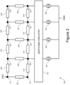
- Figure 2 is a schematic diagram of DAC circuitry 200 as a comparative example.
- DAC circuitry 200 is the same as DAC circuitry 100 except for the additional impedances and connections along the top of Figure 2 .
- Like reference numerals have been given to elements corresponding to elements in DAC circuitry 100 (with a "2" at the start instead of a "1").
- the elements corresponding to elements in DAC circuitry 100 will not be described and only the differences of DAC circuitry 200 compared to DAC circuitry 100 will be described.
- DAC circuitry 200 comprises a succession of first and further common nodes 231, 233, 235, 237 and 239, each successive further common node 233, 235, 237 and 239 connected to its preceding common node via a common impedance 232, 234, 236, and 238. That is, the further common node 233 is connected to its preceding common node (the first common node) 231 via the common impedance 232, and so on and so forth.
- the common nodes 231, 233, 235, 237 and 239 are connected to the load nodes 221, 223, 225, 227, and 229 via the load impedances 251, 253, 255, 257, and 259, respectively.
- the first common node 231 is connected to the high voltage reference AVD in line with Figure 1 .
- the common impedances 232, 234, 236, and 238 (which may be or comprise resistors) cause a voltage drop to prevent overvoltage.
- the common impedances 232, 234, 236, and 238 impact the binary ratio of the R2R ladder in the running example and as such the DAC circuitry 200 does not properly function as an R2R ladder.
- FIG. 3 is a schematic diagram of differential circuitry 300.
- Differential circuitry 300 may be referred to as DAC circuitry.
- Differential circuitry 300 comprises a first current path comprising a succession of first and further load nodes 11, 13, 15, 17, and 19, each successive further load node 13, 15, 17, and 19 connected to its preceding load node via a divider impedance 12, 14, 16, and 18. That is, the further load node 13 is connected to its preceding load node (the first load node) 11 via the divider impedance 12, and so on and so forth.
- Differential circuitry 300 comprises a second current path similarly comprising a succession of first and further load nodes 21, 23, 25, 27, and 29, each successive further load node 23, 25, 27, and 29 connected to its preceding load node via a divider impedance 22, 24, 26, and 28. That is, the further load node 23 is connected to its preceding load node (the first load node) 21 via the divider impedance 22, and so on and so forth.
- the first load nodes 11 and 21 of the first and second current paths comprise (and may be referred to as) a first pair of load nodes.
- Each successive further load node 13, 15, 17, and 19 of the first current path and its corresponding successive further load node 23, 25, 27, and 29 of the second current path comprise (and may be referred to as) a successive further pair of load nodes.
- further load nodes 13 and 23 constitute a further pair of load nodes.
- further load nodes 15 and 25 constitute a further pair of load nodes.
- the nodes of the first pair of load nodes 11 and 21 are each connected to a first common node 31 via respective first load impedances 41 and 51.
- Each successive further pair of load nodes 13, 23, 15, 25, 17, 27, 19, and 29 are connected to a successive further common node 33, 35, 37, and 39 via respective further load impedances 43, 53, 45, 55, 47, 57, 49, and 59. That is, the load node 13 of the first current path is connected to the common node 33 via the load impedance 43 and the load node 23 of the second current path is connected to the common node 33 via the load impedance 53, and so on and so forth.
- Each further common node 33, 35, 37, and 39 is connected to its preceding common node via a common impedance 32, 34, 36, and 38. That is, the common node 33 is connected to its preceding common node (the first common node) 31 via the common impedance 32, and so on and so forth.
- the divider impedances 12, 14, 16, 18, 22, 24, 26, and 28 may be or comprise resistors.
- the load impedances 41, 51, 43, 53, 45, 55, 47, 57, 49, and 59 may be or comprise resistors.
- the common impedances 32, 34, 36, and 38 may be or comprise resistors.
- the common impedances 32, 34, 36, and 38 may have a capacitance component and/or may be referred to as impedances, and/or may be referred to as discrete impedances, but in any case they have a resistance component and may be referred to as resistors.
- Differential circuitry 300 further comprises first switching circuitry 60 and a first plurality of current sources 83, 85, 87, and 89, and second switching circuitry 70 and a second plurality of current sources 93, 95, 97, and 99.
- the first switching circuitry 60 is connected between the further load nodes 13, 11, 17, and 19 of the first current path and the current sources 83, 85, 87, and 89.
- the second switching circuitry 70 is connected between the further load nodes 23, 21, 27, and 29 of the second current path and the current sources 93, 95, 97, and 99.
- the first switching circuitry 60 may be taken to comprise the current sources 83, 85, 87, and 89, or may be considered separate from the current sources.
- the second switching circuitry 70 may be taken to comprise the current sources 93, 95, 97, and 99, or may be considered separate from the current sources.
- the first common node 31 is connected to a voltage reference AVD (or VDD) in line with Figures 1 and 2 .
- the first load nodes 11 and 21 are connected respectively to first and second output nodes (not shown).
- the first load nodes 11 and 21 can be considered to be first and second output nodes, respectively.
- the current sources 83, 85, 87, 89, 93, 95, 97, and 99 are connected to a voltage reference lower than the voltage reference AVD (e.g. shown as GND) in line with Figures 1 and 2 , i.e. at the uppermost and lowermost rails in Figure 3 .
- GND voltage reference lower than the voltage reference AVD
- the AVD and GND voltage levels will depend on the application, and the circuitry could be implemented "the other way up" i.e. with the values of AVD and GND reversed.
- Differential circuitry 300 is configured to output a differential analogue output signal at (between) the output nodes indicative of a differential digital input signal. This is achieved by the first and second switching circuitry 60 and 70 which are configured to change, based on control signals, a magnitude of controllable current signals passing through the load nodes 11, 13, 15, 17, and 19 of the first current path and through the load nodes 21, 23, 25, 27, and 29 of the second current path.
- the control signals are indicative of the differential digital input signal.
- the control signals may be controlled/supplied by a controller (not shown).
- the first switching circuitry 60 comprises a plurality of switches, each switch connected between a corresponding one of the further load nodes 13, 15, 17, and 19 and a corresponding one of the current sources 83, 85, 87, and 89 (e.g. between load node 13 and current source 83).
- the second switching circuitry 70 comprises a plurality of switches, each switch connected between a corresponding one of the further load nodes 23, 25, 27, and 29 and a corresponding one of the current sources 93, 95, 97, and 99.
- the switches correspond to different data bits of the differential digital input signal and the setting of each switch is by the corresponding data bit.
- the switches corresponding to a pair of the load nodes may be considered a pair of switches and each pair of switches corresponds to a different data bit of the differential digital input signal.
- the further pairs of load nodes 13, 23, 15, 25, 17, 27, 19, and 29 may be associated with the corresponding different bits of the differential digital input signal and may be labelled as LSB (least significant bit) 3, LSB2, LSB1, and LSB0, respectively (in line with Figures 1 and 2 ).
- Differential circuitry 300 may comprise further connections shown by broken lines and further current sources 81 and 91.
- the first switching circuitry 60 and the second switching circuitry 70 may comprise a further pair of switches corresponding and connected to the first pair of load nodes 11 and 21, and to the current sources 81 and 91.
- This further pair of switches (and also the first pair of load nodes 11 and 21) may correspond to a bit of the differential digital input signal, for example the most significant bit (MSB).
- MSB most significant bit
- FIG. 4 is a schematic diagram of switching circuitry 301.
- Switching circuitry 301 illustrates an example of a part of the first switching circuitry 60 and the second switching circuitry 70.
- Switching circuitry 301 comprises one of the pairs of switches, in particular a first switch 63 connected between the load node 13 (at its drain terminal) and the current source 93 (at its source terminal), and a second switch 73 connected between the load node 23 (at its drain terminal) and the current source 93 (at its source terminal).
- the first switch 63 belongs to the first switching circuitry 60 and the second switch 73 belongs to the second switching circuitry 70.
- Switching circuitry 301 as illustrated further comprises the load impedances 43 and 45.
- the further connections of the load impedance 43 and 53 and of the load nodes 13 and 23 are not illustrated for simplicity of illustration and instead broken lines are used.
- the first and second switches 63 and 73 are connected to the same current source 93 in Figure 4 .
- Figure 3 shows the first switching circuitry 60 connected to a different current source to the second switching circuitry 70.
- the switches may share the same current source (as shown in Figure 4 ) or may use different current sources (as shown in Figure 3 ).
- each pair of switches corresponds to a data bit of the differential digital input signal.
- the first switch 63 is controlled by a control signal (at its gate terminal) labelled DATA and the second switch 73 is controlled by a complementary control signal (at its gate terminal) labelled /DATA.
- the control signals DATA and /DATA may be considered to represent a bit of the differential digital input signal. When DATA is high (or logic 1) /DATA is low (or logic 0) and vice versa.
- the other pairs of switches in differential circuitry 300 illustrated in Figure 3 may have the same or similar structures and connections as those shown in Figure 4 .
- each pair of switches may be considered to belong to a "slice" of the differential circuitry 300. Each such slice may be taken to comprise the pair of switches, and a pair of current sources (or a single shared current source in line with Figure 4 ) connected to those switches. It may therefore be considered that the current flowing from the supply (controlled by the pair of current sources considered together, or by the single shared current source in line with Figure 4 ) to the slice is fixed for each slice.
- the common impedances 32, 34, 36, and 38 each have a resistance value of r
- the divider impedances 12, 22, 14, 24, 16, 26, 18, and 28 each have a resistance value of R
- the load impedances 41 and 51 each have a resistance value of R0
- the load impedances 43, 53, 45, 55, 47 and 57 each have a resistance value of 2R
- the load impedances 49 and 59 each have a resistance value of R.
- the R2R binary weighting scheme need not be employed and the impedances may adopt other resistance values.
- the current caused to flow through output node 21 by the corresponding current source is 71, where I is the current caused to flow through each of the load nodes 23, 25, and 27 by the respective corresponding current sources.
- I the current caused to flow through each of the load nodes 23, 25, and 27 by the respective corresponding current sources.
- the load impedances 47 and 57 each have a resistance value of R (and not2R).
- R 150 Ohms
- R0 60 Ohms
- r (50/3) Ohms ⁇ 17 Ohms.
- the differential circuitry 300 achieves a number of advantages.
- the common impedances 32, 34, 36, and 38 provide fixed DC voltage drops across the successive further common nodes 33, 35, 37, and 39 (i.e. from one to the next) which do not change with the differential digital input signal. This in turn will lower the maximum voltages at the successive further load nodes 13, 15, 17, and 19 and the successive further load nodes 23, 25, 27, and 29, with those maximum voltages being lower from one successive further load node to the next. This therefore solves or at least partly addresses the overvoltage problem described above with reference to Figures 2 and 3 (i.e. the components (switches) are better protected).
- the maximum voltages at the load nodes 19 and 29 will be lower given the presence of the common impedances 32, 34, 36, and 38 than they would be without the presence of the common impedances 32, 34, 36, and 38, thereby offering some overvoltage protection to the switches (corresponding to switches 63/73 in Figure 4 ) connected to those nodes.
- the voltage drop produced by the common impedances 32, 34, 36, and 38 will change the current contribution from each slice, but since the voltage drops mentioned above are DC voltage drops the change in current contribution from each slice will be a DC change and will not affect the differential analogue output signal (current).
- the differential circuitry 300 addresses the overvoltage problem described with reference to Figures 2 and 3 , improves performance compared to the DAC circuitry 100 and 200 illustrated in Figures 2 and 3 , and functions with appropriate weightings between each slice (i.e. analogously to an R2R ladder/network) so as to be suitable for incorporation into or operation as a DAC.
- the load impedances 47 and 57 each have a resistance value of R (and not 2R).
- the load nodes 17, 27 correspond to LSB0
- the load nodes 15, 25 correspond to LSB1
- the load nodes 13, 23 correspond to LSB2
- the load nodes 11, 21 correspond to a combination of the top 3 MSB bits (e.g. with the current sources 81/91 and associated switches of the switching circuitry 60, 70 representative of 7 MSB slices controlled by thermometer decoded signals).
- a data signal D0 for the switches of LSB0 (at load nodes 17, 27) was toggled at 1 GHz
- a data signal D1 for the switches of LSB1 was toggled at 0.5 GHz
- a data signal D2 for the switches of LSB2 (at load nodes 11, 21) was toggled at 0.25 GHz
- data signals for the upper 3 MSB bits were kept static.
- Figure 5 is a graph useful for understanding the differential circuitry 300 (in its simpler form), and focusses on LSB0.
- the broken lines in each plot show, over time, the voltage at the load node 17 and the solid lines show, over time, the voltage at the load node 27.
- these graphs were obtained by keeping the values of the D1 and D2 (and the MSB data signals) fixed and only toggling the values of the D0 signals (i.e. D0 and /D0, looking at Figure 4 ).
- Figure 6 is a graph useful for understanding the differential circuitry 300 (in its simpler form), and like Figure 5 focusses on LSB0.
- the simulation settings e.g. the data signals
- the broken line shows how the DC voltage level at the load node 17 changes as the value of r changes and the solid line shows how the DC voltage level at the load node 27 changes also as the value of r changes. It will be appreciated that increasing the value of r reduces the DC voltage at the load nodes 17 and 27.
- the values for the load node 17 are lower than those for the load node 27 because the circuitry 300 is differential and in the case of this graph, the switch corresponding to the load node 17 is off whilst the switch corresponding to the load node 27 is on.
- Figure 7 is a graph useful for understanding the differential circuitry 300 (in its simpler form), and focusses on the LSBs (i.e. LSB0 to LSB2).
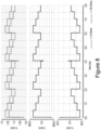
- Figure 8 is another graph useful for understanding the differential circuitry 300 (in its simpler form).
- the middle plot that the inclusion of the common impedances (i.e. r being non-zero or non-negligible, such as greater than 5 or 10 or 15 or 20 or 25 or 30 or 40 or 50 or 100 Ohms, depending on the application) does not affect the overall differential output voltage, as the solid and broken lines move together.
- the bottom plot appears "upside down” compared to the middle plot only because the differential output voltage in the bottom plot was calculated by calculating the difference between the two "sides" of differential circuitry 300 the other way round compared to the middle plot.
- Figure 9 is another graph useful for understanding the differential circuitry 300 (in its simpler form).
- the solid lines show the DC levels (or common mode voltages) at the common nodes 33, 35, and 37 and the broken lines show the DC levels (or common mode voltages) at the load nodes 13, 23, 15, 25, 17, and 27.
- the DC levels discussed above may be considered to be common mode voltages given that the differential circuitry 300 is differential.
- R and r are of course exemplary and there are many appropriate values that may be used. Furthermore, the values of for R and r may be different depending on the specific implementation of the differential circuitry 300, e.g., the maximum allowed voltage, the magnitude of the current signals flowing in the differential circuitry, etc. Furthermore, the impedances may have different values of impedance/resistance than shown.
- the differential circuitry 300 may comprise more or fewer slices than as described above and shown in Figure 3 .
- the differential circuitry 300 may comprise just the slices corresponding to the common nodes 31 and 33.
- the differential circuitry 300 may comprise fewer of the common impedances 32, 34, 36, and 38 than as described in the examples above.
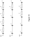
- Figure 10 is a schematic diagram showing three possible variations of a portion of the differential circuitry 300 of Figure 3 .
- the upper variation corresponds to Figure 3 itself, and all of the common impedances 32, 34, 36, and 38 are provided.
- the differential circuitry 300 may comprise only one of the common impedances 32, 34, 36, and 38 or any number of the common impedances, for example only common impedance 38 as in the middle variation, or only a plurality of the common impedances such as 36 and 38 as in the lower variation.
- the further common nodes 33, 35, 37, and 39 may be connected to its preceding common node via a common impedance 32, 34, 36, and 38 and the or each other further common node may be shorted or short-circuited to its preceding common node (i.e. a connection that is not via a resistor, or any other component). It may be said that the or each other further common node may be directly connected to its preceding common node, with "directly connected” meaning not connected via a resistor or a discrete impedance (or any other discrete component), or connected via a substantially zero resistance connection or a low or negligible impedance/resistance connection.
- the common impedances 32, 34, 36, and 38 are resistors in the running example (and may be referred to as discrete impedances, but having a resistance component) and are different from unavoidable (negligible) impedance in a circuit, e.g. of a wire connecting two components.
- Each of the common impedances 32, 34, 36, and 38, the load impedances 41, 51, 43, 53, 45, 55, 47, 57, 49, and 59, and the divider impedances 12, 22, 14, 24, 16, 26, 18, and 28 may be a discrete impedance, or a resistor, or a discrete resistor/resistance (bearing in mind that the common impedances 32, 34, 36, and 38 are or comprise resistors). These impedances are different from unavoidable impedance in a circuit, e.g. of a wire connecting two components. Any of these resistors may be implemented as polysilicon resistors, and/or as a discrete resistor or a distributed resistor.
- the switches of the first and second switching circuitry 60 and 70 may be transistors, in particular FET transistors.
- they may be MOSFET transistors.
- the slices of differential circuitry 300 described above may correspond to any bit or bits of a differential digital input signal and not only the bits as described above.
- Figure 11 is a schematic diagram of a DAC 400 comprising the differential circuitry 300.
- the slices of the differential circuitry 300 may correspond to bits of a differential digital input signal and the switches in differential circuitry 300 change, based on the bits of the differential digital input signal, a magnitude of the controllable current signals passing through the load nodes of differential circuitry 300 to ultimately output a differential analogue output signal between the first and second output nodes.
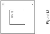
- Figure 12 is a schematic diagram illustrating an integrated circuit (IC) 500 comprising the differential circuitry 300 or the DAC 400.
- IC integrated circuit
- Circuitry of the present invention may be implemented as integrated circuitry, for example on an IC chip such as a flip chip.
- the present invention extends to integrated circuitry and IC chips as mentioned above, circuit boards comprising such IC chips, and communication networks (for example, internet fiber-optic networks and wireless networks) and network equipment of such networks, comprising such circuit boards.
- various features may be implemented in hardware, or as software modules running on one or more processors/computers.
- the invention also provides a computer program or a computer program product comprising instructions which, when executed by a computer, cause the computer to carry out (as a method) any functionality described herein, and a non-transitory computer-readable medium comprising instructions which, when executed by a computer, cause the computer to carry out any of the functionality described herein.
- a computer program embodying the invention may be stored on a non-transitory computer-readable medium, or it could, for example, be in the form of a signal such as a downloadable data signal provided from an Internet website, or it could be in any other form.
Landscapes
- Engineering & Computer Science (AREA)
- Theoretical Computer Science (AREA)
- Analogue/Digital Conversion (AREA)
Abstract
Description
- The present invention relates to differential circuitry, for example for use in a digital-to-analogue converter (DAC), and in particular to differential circuitry able to protect components from overvoltage or reduce an impact of overvoltage on such components. Such circuitry may be implemented as integrated circuitry, for example on an IC chip.
- Overvoltage may cause errors in circuitry such as a DAC or may even cause circuitry to stop functioning properly or have a reduced life. With increasing speeds of such circuitry, and corresponding miniaturisation of semiconductor device sizes, there is ever increasing pressure on operating such circuitry accurately.
- According to an embodiment of a first aspect of the present invention, there is provided differential circuitry comprising: first and second current paths each comprising a succession of first and further load nodes, each successive further load node connected to its preceding load node via a divider impedance; and first switching circuitry connected to the further load node or nodes of the first current path, and second switching circuitry connected to the further load node or nodes of the second current path, the first and second switching circuitry configured to change/control (based on control signals) a magnitude of controllable current signals passing through the load nodes of the first current path and the second current path, respectively, wherein: the first load nodes of the first and second current paths comprise (or constitute) a first pair of load nodes, and the or each successive further load node of the first current path and its corresponding successive further load node of the second current path comprise (or constitute) a successive further pair of load nodes; the first pair of load nodes are connected to a first common node via respective first load impedances and the or each successive further pair of load nodes are connected to a successive further common node via respective further load impedances; the or each successive further common node is connected to its preceding common node; and the or at least one of the successive further common nodes is connected to its preceding common node via a resistor (impedance having at least a resistance component).
- Such circuitry can avoid problems associated with overvoltage. Such circuitry can achieve improved performance because the DC levels at the load nodes are closer to each other due to the resistor(s).
- The or at least one of the successive further common nodes may be connected to its preceding common node via one or more discrete impedances as the resistor.
- The or each other successive further common node may be shorted (or short-circuited) to its preceding common node.
- In other words, the or each other successive further common node may not be connected via a resistor to its preceding common node, or may be connected to its preceding common node via a substantially zero resistance connection or a low or negligible impedance/resistance connection.
- The differential circuitry may comprise N said successive further load nodes and N said successive further common nodes, wherein N is an integer greater than 1, wherein: for n of the successive further common node or nodes, the or each successive further common node is connected to its preceding common node via a resistor, wherein n is an integer and at least 1; and for N-n of the successive further common node or nodes, the or each successive further common node is shorted (or short-circuited) to its preceding common node.
- The value n may be 1 or N, or n may be any integer value in the
range 1≤n≤N. - The differential circuitry may comprise a plurality of said successive further load nodes and a plurality of said successive further common nodes, and each successive further common node may be connected to its preceding common node via a resistor.
- The differential circuitry may comprise a plurality of said resistors, and the resistors interconnecting said common nodes may have the same resistance values as each other.
- At least a plurality of the load impedances may have the same impedance values as each other.
- The divider impedances may have the same impedance values as each other.
- The divider impedances may be or may comprise discrete divider impedances/discrete divider resistors, and/or the load impedances may be or may comprise discrete load impedances/discrete load resistors.
- The first load nodes may be connected to first and second output nodes, respectively.
- The differential circuitry may be configured to output a differential output signal between the first and second output nodes indicative of a differential input signal.
- The first switching circuitry and the second switching circuitry may be configured to change the magnitude of the controllable current signals based on control signals indicative of a/the differential input signal.
- The first switching circuitry may comprise a plurality of switches connected to the load nodes of the first current path, respectively, and the second switching circuitry may comprise a plurality of switches connected to the load nodes of the second current path, respectively.
- The first switching circuitry may comprise a plurality of current sources connected (between a (low) voltage reference and the switches of the first switching circuitry) to define respective currents at the switches of the first switching circuitry, respectively, and the second switching circuitry may comprise a plurality of current sources connected (between a (low) voltage reference and the switches of the second switching circuitry) to define respective currents at the switches of the second switching circuitry, respectively.
- The first switching circuitry and the second switching circuitry may comprise a plurality of current sources, each current source connected (between a (low) voltage reference (wherein the low voltage references may be the same low voltage reference) and the switches connected to a said pair of loads nodes) to define respective currents at the switches connected to a said pair of load nodes.
- The switches of the first switching circuitry may be connected/configured to be controlled by control signals indicative of a first input signal, and the switches of the second switching circuitry may be connected/configured to be controlled by control signals indicative of a second input signal, the first and second input signals together corresponding to a/the differential input signal.
- The differential input signal may be a digital signal. The differential circuitry may be configured to output an analogue signal as the differential output signal, based on the digital signal.
- According to an embodiment of a second aspect of the present invention, there is provided differential circuitry comprising: first and second current paths each comprising a succession of first and further load nodes, each successive further load node connected to its preceding load node via a divider impedance, wherein: the first load nodes of the first and second current paths comprise a first pair of load nodes, and the or each successive further load node of the first current path and its corresponding successive further load node of the second current path comprise a successive further pair of load nodes; the first pair of load nodes are connected to a first common node via respective first load impedances and the or each successive further pair of load nodes are connected to a successive further common node via respective further load impedances; the or each successive further common node is connected to its preceding common node; and the or at least one of the successive further common nodes is connected to its preceding common node via a resistor.
- According to an embodiment of a third aspect of the present invention, there is provided differential circuitry comprising: first and second current paths each comprising a first load node, a second load node, and an output node, wherein the differential circuitry is configured to output a differential current signal between the output nodes; and a first switching circuit connected to the first and second load nodes of the first current path, and a second switching circuit connected to the first and second load nodes of the second current path, the first and second switching circuits configured to change (based on control signals) a magnitude of controllable current signals passing through the load nodes of the first current path and the second current path, respectively, wherein each current path comprises a first divider impedance connected between its first load node and its output node, and a second divider impedance connected between its first load node and its second load node, wherein both of the first load nodes are connected to a first common node via respective first common impedances, both of the second load nodes are connected to a second common node via respective second common impedances, and both of the output nodes are connected to a reference node via respective reference impedances, wherein the reference node is connected to a voltage reference, wherein the differential circuitry further comprises a first common impedance/resistor connected between the reference node and the first common node, and a second common impedance/resistor connected between the first and second common nodes.
- According to an embodiment of a fourth aspect of the present invention, there is provided digital-to-analogue converter, DAC, circuitry comprising the differential circuitry of any of the first to third aspects.
- According to an embodiment of a fifth aspect of the present invention, there is provided integrated circuitry such as an IC chip, comprising the differential circuitry of any of the first to third aspects or the DAC circuitry of the fourth aspect.
- Reference will now be made, by way of example, to the accompanying drawings, of which:
-
Figure 1 is a schematic diagram of DAC circuitry as a comparative example; -
Figure 2 is a schematic diagram of DAC circuitry as a comparative example; -
Figure 3 is a schematic diagram of differential circuitry; -
Figure 4 is a schematic diagram of switching circuitry; -
Figure 5 is a graph useful for understandingFigure 3 ; -
Figure 6 is a graph useful for understandingFigure 3 ; -
Figure 7 is a graph useful for understandingFigure 3 ; -
Figure 8 is a graph useful for understandingFigure 3 ; -
Figure 9 is a diagram useful for understandingFigure 3 ; -
Figure 10 is a diagram useful for understanding variations ofFigure 3 ; -
Figure 11 is a schematic diagram of a DAC; and -
Figure 12 is a schematic diagram of integrated circuitry. -
Figure 1 is a schematic diagram ofDAC circuitry 100 as a comparative example.DAC circuitry 100 comprises a succession of first andfurther load nodes further load node divider impedance further load node 123 is connected to its preceding load node (the first load node) 121 via thedivider impedance 122, and so on and so forth. -
DAC circuitry 100 further comprises a plurality ofload impedances load nodes load impedance 151 is connected between the voltage reference AVD and theload node 121, theload impedance 153 is connected between the voltage reference AVD and theload node 123, and so on and so forth. - DAC circuitry further comprises switching
circuitry 170 and a plurality ofcurrent sources switching circuitry 170 is connected between thefurther load nodes current sources current sources - The
first load node 121 is connected to an output node (not shown). Thefirst load node 121 may be considered to be the output node. -
DAC circuitry 100 is configured to output an analogue output signal at the output node indicative of a digital input signal. This is achieved by theswitching circuitry 170 which is configured to change, based on control signals (not shown), a magnitude of controllable current signals passing through theload nodes switching circuitry 170 comprises a plurality of switches, each switch connected between a corresponding one of thefurther load nodes current sources load node 123 and current source 193). The switches correspond to different data bits of the digital input signal and the setting of the switch is by the corresponding data bit. For this reason thefurther load nodes -
DAC circuitry 100 can be considered to be (or to comprise) an R2R network/ladder or an R2R circuit or R2R circuitry. That is, in order to effect binary weighting theimpedances impedances relative resistance 2R, and this will be carried forwards as a running example. - The voltage levels at the
further load nodes switching circuitry 170 turn on and off because the current through the R2R ladder varies due to contributions from differentcurrent sources further load nodes load node 129 may be higher than that at the load node 123). This voltage level (e.g. the load node 129) can be higher than the rating of the components (i.e. the switches) used in the design which can lead to overvoltage. This can cause errors in the operation of theDAC circuitry 100 or cause theDAC circuitry 100 to stop working properly or have a reduced life. - Furthermore the difference in DC level (common mode voltage) across or at the
further load nodes Figure 9 ). -
Figure 2 is a schematic diagram ofDAC circuitry 200 as a comparative example. -
DAC circuitry 200 is the same asDAC circuitry 100 except for the additional impedances and connections along the top ofFigure 2 . Like reference numerals have been given to elements corresponding to elements in DAC circuitry 100 (with a "2" at the start instead of a "1"). The elements corresponding to elements inDAC circuitry 100 will not be described and only the differences ofDAC circuitry 200 compared toDAC circuitry 100 will be described. -
DAC circuitry 200 comprises a succession of first and furthercommon nodes common node common impedance common node 233 is connected to its preceding common node (the first common node) 231 via thecommon impedance 232, and so on and so forth. Thecommon nodes load nodes load impedances common node 231 is connected to the high voltage reference AVD in line withFigure 1 . - The
common impedances common impedances DAC circuitry 200 does not properly function as an R2R ladder. -
Figure 3 is a schematic diagram ofdifferential circuitry 300.Differential circuitry 300 may be referred to as DAC circuitry.Differential circuitry 300 comprises a first current path comprising a succession of first andfurther load nodes further load node divider impedance further load node 13 is connected to its preceding load node (the first load node) 11 via thedivider impedance 12, and so on and so forth. -
Differential circuitry 300 comprises a second current path similarly comprising a succession of first andfurther load nodes further load node divider impedance further load node 23 is connected to its preceding load node (the first load node) 21 via thedivider impedance 22, and so on and so forth. - The
first load nodes further load node further load node further load nodes further load nodes - The nodes of the first pair of
load nodes common node 31 via respectivefirst load impedances load nodes common node further load impedances load node 13 of the first current path is connected to thecommon node 33 via theload impedance 43 and theload node 23 of the second current path is connected to thecommon node 33 via theload impedance 53, and so on and so forth. - Each further
common node common impedance common node 33 is connected to its preceding common node (the first common node) 31 via thecommon impedance 32, and so on and so forth. - The divider impedances 12, 14, 16, 18, 22, 24, 26, and 28 may be or comprise resistors. The load impedances 41, 51, 43, 53, 45, 55, 47, 57, 49, and 59 may be or comprise resistors. The
common impedances common impedances -
Differential circuitry 300 further comprises first switchingcircuitry 60 and a first plurality ofcurrent sources second switching circuitry 70 and a second plurality ofcurrent sources first switching circuitry 60 is connected between thefurther load nodes current sources second switching circuitry 70 is connected between thefurther load nodes current sources - The
first switching circuitry 60 may be taken to comprise thecurrent sources second switching circuitry 70 may be taken to comprise thecurrent sources - The first
common node 31 is connected to a voltage reference AVD (or VDD) in line withFigures 1 and2 . Thefirst load nodes first load nodes current sources Figures 1 and2 , i.e. at the uppermost and lowermost rails inFigure 3 . Of course, the AVD and GND voltage levels will depend on the application, and the circuitry could be implemented "the other way up" i.e. with the values of AVD and GND reversed. -
Differential circuitry 300 is configured to output a differential analogue output signal at (between) the output nodes indicative of a differential digital input signal. This is achieved by the first andsecond switching circuitry load nodes load nodes - In particular, although not shown, the
first switching circuitry 60 comprises a plurality of switches, each switch connected between a corresponding one of thefurther load nodes current sources load node 13 and current source 83). Furthermore, thesecond switching circuitry 70 comprises a plurality of switches, each switch connected between a corresponding one of thefurther load nodes current sources load nodes Figures 1 and2 ). -
Differential circuitry 300 may comprise further connections shown by broken lines and furthercurrent sources first switching circuitry 60 and thesecond switching circuitry 70 may comprise a further pair of switches corresponding and connected to the first pair ofload nodes current sources load nodes 11 and 21) may correspond to a bit of the differential digital input signal, for example the most significant bit (MSB). Of course, the number of bits implemented at each pair of load nodes, and indeed the number of pairs of load nodes provided, will differ from implementation to implementation, and the arrangement inFigure 3 is simply an example. -
Figure 4 is a schematic diagram of switchingcircuitry 301.Switching circuitry 301 illustrates an example of a part of thefirst switching circuitry 60 and thesecond switching circuitry 70.Switching circuitry 301 comprises one of the pairs of switches, in particular afirst switch 63 connected between the load node 13 (at its drain terminal) and the current source 93 (at its source terminal), and asecond switch 73 connected between the load node 23 (at its drain terminal) and the current source 93 (at its source terminal). Thefirst switch 63 belongs to thefirst switching circuitry 60 and thesecond switch 73 belongs to thesecond switching circuitry 70. -
Switching circuitry 301 as illustrated further comprises the load impedances 43 and 45. The further connections of theload impedance load nodes - However it will be appreciated how the switching
circuitry 301 is a part of thedifferential circuitry 300 by referring toFigure 3 of thedifferential circuitry 300. - The first and
second switches current source 93 inFigure 4 .Figure 3 shows thefirst switching circuitry 60 connected to a different current source to thesecond switching circuitry 70. For each pair of switches in the first andsecond switching circuitry Figure 4 ) or may use different current sources (as shown inFigure 3 ). - As mentioned above with reference to
Figure 3 , each pair of switches corresponds to a data bit of the differential digital input signal. As illustrated inFigure 4 , thefirst switch 63 is controlled by a control signal (at its gate terminal) labelled DATA and thesecond switch 73 is controlled by a complementary control signal (at its gate terminal) labelled /DATA. The control signals DATA and /DATA may be considered to represent a bit of the differential digital input signal. When DATA is high (or logic 1) /DATA is low (or logic 0) and vice versa. - The other pairs of switches in
differential circuitry 300 illustrated inFigure 3 may have the same or similar structures and connections as those shown inFigure 4 . - Returning to
Figure 3 , for each pair of switches, as one switch is turned on and current is thus contributed to the corresponding current path the other switch is turned off. Therefore the current flowing from a given pair of current sources is fixed assuming the pair of current sources concerned have the same current magnitude as one another or assuming that the pair of current sources concerned is implemented as a single shared current source in line withFigure 4 . Each pair of switches may be considered to belong to a "slice" of thedifferential circuitry 300. Each such slice may be taken to comprise the pair of switches, and a pair of current sources (or a single shared current source in line withFigure 4 ) connected to those switches. It may therefore be considered that the current flowing from the supply (controlled by the pair of current sources considered together, or by the single shared current source in line withFigure 4 ) to the slice is fixed for each slice. - In a running example (in line with that mentioned earlier), the
common impedances - Considering an example implementation of the
differential circuitry 300 with the elements within the dashedbox 310 not provided (i.e. in particular configured as a 6-bit DAC), the current caused to flow throughoutput node 21 by the corresponding current source is 71, where I is the current caused to flow through each of theload nodes differential circuitry 300, i.e. for theoutput node 11 and theload nodes box 310 not provided), the load impedances 47 and 57 each have a resistance value of R (and not2R). In such an implementation the following values for R, R0 and r lead to improved performance: R = 150 Ohms, R0 = 60 Ohms, and r = (50/3) Ohms ≈ 17 Ohms. - The
differential circuitry 300 achieves a number of advantages. - The
common impedances common nodes further load nodes further load nodes Figures 2 and3 (i.e. the components (switches) are better protected). For example, the maximum voltages at theload nodes common impedances common impedances switches 63/73 inFigure 4 ) connected to those nodes. - This fixed DC voltage drop compensates for the variation in the DC levels (common mode voltage) across the network of impedances (including the common, load, and divider impedances) which otherwise affects the current contribution from each slice and degrades performance (as explained below in relation to
Figure 9 ). - Incidentally, the voltage drop produced by the
common impedances - In summary, the
differential circuitry 300 addresses the overvoltage problem described with reference toFigures 2 and3 , improves performance compared to theDAC circuitry Figures 2 and3 , and functions with appropriate weightings between each slice (i.e. analogously to an R2R ladder/network) so as to be suitable for incorporation into or operation as a DAC. - The graphs in
Figures 5 to 9 will now be described. These graphs were obtained by simulating a simpler form of thedifferential circuitry 300, in particular configured as a 6-bit DAC and with the elements within the dashedbox 310 not provided. In such an implementation and in line with the running example, the load impedances 47 and 57 each have a resistance value of R (and not 2R). Thus, in the implementation as simulated, theload nodes load nodes load nodes load nodes current sources 81/91 and associated switches of the switchingcircuitry - Furthermore, in the simulation (unless stated otherwise) a data signal D0 for the switches of LSB0 (at
load nodes 17, 27) was toggled at 1 GHz, a data signal D1 for the switches of LSB1 (atload nodes 15, 25) was toggled at 0.5 GHz and a data signal D2 for the switches of LSB2 (atload nodes 11, 21) was toggled at 0.25 GHz, and data signals for the upper 3 MSB bits were kept static. - It is also assumed that the
common impedances -
Figure 5 is a graph useful for understanding the differential circuitry 300 (in its simpler form), and focusses on LSB0. The broken lines in each plot show, over time, the voltage at theload node 17 and the solid lines show, over time, the voltage at theload node 27. The top plot shows the voltages when r = 0 Ohms and the bottom plot shows the voltages when r = 50 Ohms. For simplicity, these graphs were obtained by keeping the values of the D1 and D2 (and the MSB data signals) fixed and only toggling the values of the D0 signals (i.e. D0 and /D0, looking atFigure 4 ). - It will be appreciated from
Figure 5 that the voltage is at a lower level at both of theload nodes -
Figure 6 is a graph useful for understanding the differential circuitry 300 (in its simpler form), and likeFigure 5 focusses on LSB0. The simulation settings (e.g. the data signals) were the same as forFigure 5 . The broken line shows how the DC voltage level at theload node 17 changes as the value of r changes and the solid line shows how the DC voltage level at theload node 27 changes also as the value of r changes. It will be appreciated that increasing the value of r reduces the DC voltage at theload nodes load node 17 are lower than those for theload node 27 because thecircuitry 300 is differential and in the case of this graph, the switch corresponding to theload node 17 is off whilst the switch corresponding to theload node 27 is on. -
Figure 7 is a graph useful for understanding the differential circuitry 300 (in its simpler form), and focusses on the LSBs (i.e. LSB0 to LSB2). The solid lines show the voltages at theload nodes -
Figure 8 is another graph useful for understanding the differential circuitry 300 (in its simpler form). - In the top plot the solid line shows the voltage at the
load node 13 when r = 0 Ohms and the broken line shows the voltage at theload node 13 when r = 50 Ohms. It will be appreciated that the voltage is lower when r = 50 Ohms compared to when r = 0 Ohms. - In the middle plot, the solid line shows the differential voltage signal between the
load nodes load nodes - In the bottom plot, the solid line shows the overall differential voltage output of the differential circuitry 300 (i.e. between the output nodes, effectively between
nodes 11 and 21) when r = 0 Ohms and the broken line shows the same overall differential voltage output when r = 50 Ohms. It will be appreciated, as for the middle plot, that the inclusion of the common impedances (i.e. r being non-zero or non-negligible, such as greater than 5 or 10 or 15 or 20 or 25 or 30 or 40 or 50 or 100 Ohms, depending on the application) does not affect the overall differential output voltage, as the solid and broken lines move together. The bottom plot appears "upside down" compared to the middle plot only because the differential output voltage in the bottom plot was calculated by calculating the difference between the two "sides" ofdifferential circuitry 300 the other way round compared to the middle plot. -
Figure 9 is another graph useful for understanding the differential circuitry 300 (in its simpler form). The solid lines show the DC levels (or common mode voltages) at thecommon nodes load nodes - Looking at the solid lines, the DC level is the same at the
common nodes common nodes - Looking at the broken lines, the DC levels at the
load nodes load nodes - The DC levels at the
load nodes - The DC levels discussed above may be considered to be common mode voltages given that the
differential circuitry 300 is differential. - The values used above for R and r are of course exemplary and there are many appropriate values that may be used. Furthermore, the values of for R and r may be different depending on the specific implementation of the
differential circuitry 300, e.g., the maximum allowed voltage, the magnitude of the current signals flowing in the differential circuitry, etc. Furthermore, the impedances may have different values of impedance/resistance than shown. - The
differential circuitry 300 may comprise more or fewer slices than as described above and shown inFigure 3 . For example, thedifferential circuitry 300 may comprise just the slices corresponding to thecommon nodes - Alternatively or additionally, the
differential circuitry 300 may comprise fewer of thecommon impedances Figure 10 is a schematic diagram showing three possible variations of a portion of thedifferential circuitry 300 ofFigure 3 . The upper variation corresponds toFigure 3 itself, and all of thecommon impedances differential circuitry 300 may comprise only one of thecommon impedances common impedance 38 as in the middle variation, or only a plurality of the common impedances such as 36 and 38 as in the lower variation. These are simply examples and other variations are of course possible looking atFigure 10 . That is, only one (or each of any number) of the furthercommon nodes common impedance common impedances - Each of the
common impedances common impedances - The switches of the first and
second switching circuitry 60 and 70 (e.g. theswitches 63 and 73) may be transistors, in particular FET transistors. For example, they may be MOSFET transistors. - The slices of
differential circuitry 300 described above may correspond to any bit or bits of a differential digital input signal and not only the bits as described above. -
Figure 11 is a schematic diagram of aDAC 400 comprising thedifferential circuitry 300. As mentioned above, the slices of thedifferential circuitry 300 may correspond to bits of a differential digital input signal and the switches indifferential circuitry 300 change, based on the bits of the differential digital input signal, a magnitude of the controllable current signals passing through the load nodes ofdifferential circuitry 300 to ultimately output a differential analogue output signal between the first and second output nodes. -
Figure 12 is a schematic diagram illustrating an integrated circuit (IC) 500 comprising thedifferential circuitry 300 or theDAC 400. - Circuitry of the present invention may be implemented as integrated circuitry, for example on an IC chip such as a flip chip. The present invention extends to integrated circuitry and IC chips as mentioned above, circuit boards comprising such IC chips, and communication networks (for example, internet fiber-optic networks and wireless networks) and network equipment of such networks, comprising such circuit boards.
- In any of the above aspects, various features may be implemented in hardware, or as software modules running on one or more processors/computers. The invention also provides a computer program or a computer program product comprising instructions which, when executed by a computer, cause the computer to carry out (as a method) any functionality described herein, and a non-transitory computer-readable medium comprising instructions which, when executed by a computer, cause the computer to carry out any of the functionality described herein. A computer program embodying the invention may be stored on a non-transitory computer-readable medium, or it could, for example, be in the form of a signal such as a downloadable data signal provided from an Internet website, or it could be in any other form.
Claims (15)
- Differential circuitry comprising:first and second current paths each comprising a succession of first and further load nodes, each successive further load node connected to its preceding load node via a divider impedance; andfirst switching circuitry connected to the further load node or nodes of the first current path, and second switching circuitry connected to the further load node or nodes of the second current path, the first and second switching circuitry configured to control a magnitude of controllable current signals passing through the load nodes of the first current path and the second current path, respectively,wherein:the first load nodes of the first and second current paths comprise a first pair of load nodes, and the or each successive further load node of the first current path and its corresponding successive further load node of the second current path comprise a successive further pair of load nodes;the first pair of load nodes are connected to a first common node via respective first load impedances and the or each successive further pair of load nodes are connected to a successive further common node via respective further load impedances;the or each successive further common node is connected to its preceding common node; andthe or at least one of the successive further common nodes is connected to its preceding common node via a resistor.
- The differential circuitry as claimed in claim 1, wherein the or each other successive further common node is shorted to its preceding common node.
- The differential circuitry as claimed in claim 1 or 2, comprising N said successive further load nodes and N said successive further common nodes, wherein N is an integer greater than 1,
wherein:for n of the successive further common node or nodes, the or each successive further common node is connected to its preceding common node via a resistor, wherein n is an integer and at least 1; andfor N-n of the successive further common node or nodes, the or each successive further common node is shorted to its preceding common node. - The differential circuitry as claimed in claim 3, wherein:n is 1 or N; orn is 1≤n≤N.
- The differential circuitry as claimed in claim 1 or claim 2, wherein each successive further common node is connected to its preceding common node via a resistor.
- The differential circuitry as claimed in any of the preceding claims, wherein the resistors interconnecting said common nodes have the same resistance values as each other.
- The differential circuitry as claimed in any of the preceding claims, wherein the first load nodes are connected to first and second output nodes, respectively.
- The differential circuitry as claimed in claim 7, wherein the differential circuitry is configured to output a differential output signal between the first and second output nodes indicative of a differential input signal.
- The differential circuitry as claimed in claim 8, wherein the first switching circuitry and the second switching circuitry are configured to change the magnitude of the controllable current signals based on control signals indicative of the differential input signal.
- The differential circuitry as claimed in any of the preceding claims, wherein the first switching circuitry comprises a plurality of switches connected to the load nodes of the first current path, respectively, and wherein the second switching circuitry comprises a plurality of switches connected to the load nodes of the second current path, respectively.
- The differential circuitry as claimed in any of the preceding claims, wherein the first switching circuitry comprises a plurality of current sources connected to define respective currents at the switches of the first switching circuitry, respectively, and wherein the second switching circuitry comprises a plurality of current sources connected to define respective currents at the switches of the second switching circuitry, respectively.
- The differential circuitry as claimed in any of claims 1 to 10, wherein the first switching circuitry and the second switching circuitry comprise a plurality of current sources, each current source connected to define respective currents at the switches connected to a said pair of load nodes.
- The differential circuitry as claimed in any of the preceding claims, wherein the switches of the first switching circuitry are configured to be controlled by control signals indicative of a first input signal, and wherein the switches of the second switching circuitry are configured to be controlled by control signals indicative of a second input signal, the first and second input signals together corresponding to a differential input signal.
- Digital-to-analogue converter, DAC, circuitry comprising the differential circuitry as claimed in any of the preceding claims.
- Integrated circuitry such as an IC chip, comprising the differential circuitry as claimed in any of claims 1 to 13 or the DAC circuitry as claimed in claim 14.
Priority Applications (2)
| Application Number | Priority Date | Filing Date | Title |
|---|---|---|---|
| EP21203829.3A EP4170911A1 (en) | 2021-10-20 | 2021-10-20 | Differential circuitry |
| US17/959,887 US11863199B2 (en) | 2021-10-20 | 2022-10-04 | Differential circuitry |
Applications Claiming Priority (1)
| Application Number | Priority Date | Filing Date | Title |
|---|---|---|---|
| EP21203829.3A EP4170911A1 (en) | 2021-10-20 | 2021-10-20 | Differential circuitry |
Publications (1)
| Publication Number | Publication Date |
|---|---|
| EP4170911A1 true EP4170911A1 (en) | 2023-04-26 |
Family
ID=78332704
Family Applications (1)
| Application Number | Title | Priority Date | Filing Date |
|---|---|---|---|
| EP21203829.3A Pending EP4170911A1 (en) | 2021-10-20 | 2021-10-20 | Differential circuitry |
Country Status (2)
| Country | Link |
|---|---|
| US (1) | US11863199B2 (en) |
| EP (1) | EP4170911A1 (en) |
Citations (1)
| Publication number | Priority date | Publication date | Assignee | Title |
|---|---|---|---|---|
| JPH04217120A (en) * | 1990-12-18 | 1992-08-07 | Fujitsu Ltd | Digital/analog converter |
Family Cites Families (4)
| Publication number | Priority date | Publication date | Assignee | Title |
|---|---|---|---|---|
| US5781141A (en) | 1995-10-20 | 1998-07-14 | Denso Corporation | Digital-to-analog converter and sensor-characteristic adjustment circuit |
| US6593869B1 (en) * | 2002-03-28 | 2003-07-15 | Hrl Laboratories, Llc | High efficiency, high output drive current switch with application to digital to analog conversion |
| TWI370620B (en) | 2007-11-15 | 2012-08-11 | Univ Chung Yuan Christian | Folded r-2r ladder current-steering digital to analog converter |
| US10797720B2 (en) | 2018-09-21 | 2020-10-06 | Qualcomm Incorporated | Apparatus and method for measuring current source mismatches in current-steering DAC by re-using R2R network |
-
2021
- 2021-10-20 EP EP21203829.3A patent/EP4170911A1/en active Pending
-
2022
- 2022-10-04 US US17/959,887 patent/US11863199B2/en active Active
Patent Citations (1)
| Publication number | Priority date | Publication date | Assignee | Title |
|---|---|---|---|---|
| JPH04217120A (en) * | 1990-12-18 | 1992-08-07 | Fujitsu Ltd | Digital/analog converter |
Non-Patent Citations (1)
| Title |
|---|
| WEISS F G ET AL: "A 14-bit, 1 Gs/s DAC for direct digital synthesis applications", GALLIUM ARSENIDE INTEGRATED CIRCUIT (GAAS IC) SYMPOSIUM, 1991. TECHNIC AL DIGEST 1991., 13TH ANNUAL MONTEREY, CA, USA 20-23 OCT. 1991, NEW YORK, NY, USA,IEEE, US, 20 October 1991 (1991-10-20), pages 361 - 364, XP010053241, ISBN: 978-0-7803-0196-2, DOI: 10.1109/GAAS.1991.172714 * |
Also Published As
| Publication number | Publication date |
|---|---|
| US11863199B2 (en) | 2024-01-02 |
| US20230123260A1 (en) | 2023-04-20 |
Similar Documents
| Publication | Publication Date | Title |
|---|---|---|
| CN106209108B (en) | Segmented DAC | |
| US9397635B2 (en) | Segmented attenuator with glitch reduction | |
| US20100072821A1 (en) | Semiconductor device | |
| US10944417B1 (en) | Radio frequency DAC with improved linearity using shadow capacitor switching | |
| CN110456850B (en) | Semiconductor device, method of manufacturing the same, and method of operating the same | |
| US20130342241A1 (en) | Pseudo-Supply Hybrid Driver | |
| JP7542002B2 (en) | Voltage driver and method of operation thereof | |
| US8937568B2 (en) | D/A converter | |
| US8896473B2 (en) | Digital-to-analog-converter with resistor ladder | |
| US11863199B2 (en) | Differential circuitry | |
| US6344815B2 (en) | Digital-to-analog converter | |
| JP5477093B2 (en) | DA converter | |
| KR100884591B1 (en) | On Die Termination Circuit | |
| US20120176263A1 (en) | Current switch circuit and da converter | |
| US11356114B2 (en) | R-2R resistor ladder trim circuits | |
| US7696786B2 (en) | Precision differential level shifter | |
| US6788042B2 (en) | Variable impedance network for an integrated circuit potentiometer | |
| KR102958548B1 (en) | Voltage driver with supply current stabilization function | |
| US7554475B2 (en) | Low-power inverted ladder digital-to-analog converter | |
| US20210083661A1 (en) | Variable capacitance circuit | |
| US20200259499A1 (en) | Circuit technique to improve spur-free dynamic range of a digital to analog converter | |
| CN114884530B (en) | Wired transceiver | |
| KR20010042440A (en) | A current compensating bias generator and method therefor | |
| JP2006114711A (en) | Protection circuit and semiconductor integrated circuit equipped with the same | |
| JP4876254B2 (en) | Circuit equipment |
Legal Events
| Date | Code | Title | Description |
|---|---|---|---|
| PUAI | Public reference made under article 153(3) epc to a published international application that has entered the european phase |
Free format text: ORIGINAL CODE: 0009012 |
|
| STAA | Information on the status of an ep patent application or granted ep patent |
Free format text: STATUS: THE APPLICATION HAS BEEN PUBLISHED |
|
| AK | Designated contracting states |
Kind code of ref document: A1 Designated state(s): AL AT BE BG CH CY CZ DE DK EE ES FI FR GB GR HR HU IE IS IT LI LT LU LV MC MK MT NL NO PL PT RO RS SE SI SK SM TR |
|
| STAA | Information on the status of an ep patent application or granted ep patent |
Free format text: STATUS: REQUEST FOR EXAMINATION WAS MADE |
|
| 17P | Request for examination filed |
Effective date: 20231025 |
|
| RBV | Designated contracting states (corrected) |
Designated state(s): AL AT BE BG CH CY CZ DE DK EE ES FI FR GB GR HR HU IE IS IT LI LT LU LV MC MK MT NL NO PL PT RO RS SE SI SK SM TR |