EP4170371A1 - Magnetic sensor array - Google Patents
Magnetic sensor array Download PDFInfo
- Publication number
- EP4170371A1 EP4170371A1 EP21825894.5A EP21825894A EP4170371A1 EP 4170371 A1 EP4170371 A1 EP 4170371A1 EP 21825894 A EP21825894 A EP 21825894A EP 4170371 A1 EP4170371 A1 EP 4170371A1
- Authority
- EP
- European Patent Office
- Prior art keywords
- magnetic
- sensor
- magnetic sensor
- magnetic sensors
- sensor array
- Prior art date
- Legal status (The legal status is an assumption and is not a legal conclusion. Google has not performed a legal analysis and makes no representation as to the accuracy of the status listed.)
- Pending
Links
Images



Classifications
-
- G—PHYSICS
- G01—MEASURING; TESTING
- G01R—MEASURING ELECTRIC VARIABLES; MEASURING MAGNETIC VARIABLES
- G01R33/00—Arrangements or instruments for measuring magnetic variables
- G01R33/0094—Sensor arrays
-
- G—PHYSICS
- G01—MEASURING; TESTING
- G01R—MEASURING ELECTRIC VARIABLES; MEASURING MAGNETIC VARIABLES
- G01R33/00—Arrangements or instruments for measuring magnetic variables
- G01R33/0005—Geometrical arrangement of magnetic sensor elements; Apparatus combining different magnetic sensor types
-
- G—PHYSICS
- G01—MEASURING; TESTING
- G01R—MEASURING ELECTRIC VARIABLES; MEASURING MAGNETIC VARIABLES
- G01R33/00—Arrangements or instruments for measuring magnetic variables
- G01R33/0047—Housings or packaging of magnetic sensors ; Holders
-
- G—PHYSICS
- G01—MEASURING; TESTING
- G01R—MEASURING ELECTRIC VARIABLES; MEASURING MAGNETIC VARIABLES
- G01R33/00—Arrangements or instruments for measuring magnetic variables
- G01R33/02—Measuring direction or magnitude of magnetic fields or magnetic flux
- G01R33/06—Measuring direction or magnitude of magnetic fields or magnetic flux using galvano-magnetic devices
- G01R33/09—Magnetoresistive devices
- G01R33/091—Constructional adaptation of the sensor to specific applications
-
- G—PHYSICS
- G01—MEASURING; TESTING
- G01R—MEASURING ELECTRIC VARIABLES; MEASURING MAGNETIC VARIABLES
- G01R33/00—Arrangements or instruments for measuring magnetic variables
- G01R33/0011—Arrangements or instruments for measuring magnetic variables comprising means, e.g. flux concentrators, flux guides, for guiding or concentrating the magnetic flux, e.g. to the magnetic sensor
Definitions
- the present invention relates to a magnetic sensor array including a plurality of magnetic sensors and, more particularly, to a magnetic sensor array in which the angle between the plurality of magnetic sensors is variable.
- Patent Document 1 discloses in FIG. 2 thereof a magnetic sensor array in which a plurality of magnetic sensors can be slid independently in one direction. Patent Document 1 further discloses in FIG. 14 thereof a magnetic sensor array in which a plurality of magnetic sensors are held by a holding part made of a flexible material. In these magnetic sensor arrays, a plurality of magnetic sensors can be brought close to even a curved surface of an object to be measured.
- Patent Document 1 International Publication WO 2018/025829
- a magnetic sensor array according to the present invention is a magnetic sensor array including a plurality of magnetic sensors.
- the magnetic sensors each include a sensor chip, a sensor housing body housing the sensor chip, and first and second connection parts formed on the sensor housing body.
- the first connection part formed on one of adjacent magnetic sensors and the second connection part formed on the other one thereof are axially supported on each other to achieve mutual connection between the plurality of magnetic sensors.
- the present invention it is possible to vary the relative angle between two adjacent magnetic sensors with the first and second connection parts as an axis. This allows the plurality of magnetic sensors to be pressed perpendicularly against even a curved surface of an object to be measured, and the pressed state can be easily maintained.
- the sensor housing body may have a sensor head perpendicular to the sensitivity axis direction of the magnetic sensor and first and second side surfaces parallel to the sensitivity axis direction of the magnetic sensor and positioned on mutually opposite sides, the first connection part may be formed on the first side surface at a portion in a vicinity of the sensor head, and the second connection part may be formed on the second side surface at a portion in a vicinity of the sensor head.
- the plurality of magnetic sensors may constitute a plurality of groups including first and second groups, at least one of the magnetic sensors belonging to the first group may further include a third connection part formed on the sensor housing body, at least one of the magnetic sensors belonging to the second group may further include a fourth connection part formed on the sensor housing body, and the first and second groups may be mutually connected with the third and fourth connection parts axially supported on each other.
- the sensor housing body may further have third and fourth side surfaces parallel to the sensitivity axis direction of the magnetic sensor and perpendicular to the first and second side surfaces and are positioned on mutually opposite sides, the third connection part may be formed on the third side surface at a portion in a vicinity of the sensor head, and the fourth connection part may be formed on the fourth side surface at a portion in a vicinity of the sensor head.
- a magnetic sensor array in which magnetic sensors constituting the magnetic sensor array can be pressed perpendicularly against even a curved surface of an object to be measured, and the pressed state can be easily maintained.
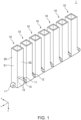
- the magnetic sensor array 1 has a configuration in which a plurality of magnetic sensors 10 each elongated in the z-direction are arranged in the x-direction.
- the sensitivity axis direction of each of the magnetic sensors 10 is along the z-direction.
- seven magnetic sensors 10 constitute the magnetic sensor array 1; however, the number of the magnetic sensors 10 constituting the magnetic sensor array 1 is not particularly limited to a specific number.
- the cancel coil C1 is disposed so as to overlap the magnetoresistance effect elements M1 to M4.
- cancel magnetic fields in mutually opposite directions are applied to the magnetoresistance effect elements M1, M2 and magnetoresistance effect elements M3, M4.
- the magnetoresistance effect elements M1 to M4 included in the magnetic sensor 10 are bridge-connected, and a differential signal generated thereby is supplied to a differential amplifier 31.
- the differential amplifier 31 generates a feedback current F1 based on the supplied differential signal.
- the feedback current F1 flows in the cancel coil C1. This causes the cancel coil C1 to generate a cancel magnetic field so as to make a differential signal component which is an output signal of the magnetic sensor 10 zero.
- the feedback current F is current-voltage converted by a resistor R, and a detection signal Vout proportional to the feedback current F is generated by a voltage measurement circuit 32 measuring the voltage across the resistor R.
- an angle ⁇ between two adjacent magnetic sensors 10 can be varied.
- the long dashed dotted lines Z1 and Z2 illustrated in FIG. 6 denotes the sensitivity axis directions of the respective two adjacent magnetic sensors 10.
- the plurality of magnetic sensors 10 are connected through the rotary shafts 15, thereby allowing the shape of the measurement surface constituted by the plurality of sensor heads to be varied in accordance with the surface shape of an object to be measured.
- FIG. 7 is a schematic perspective view illustrating the outer appearance of a magnetic sensor array 2 according to a second embodiment of the present invention.
- the magnetic sensor array 2 according to the second embodiment differs from the magnetic sensor array 1 according to the first embodiment in that connection parts 13 and 14 are formed on the sensor housing bodies 20 of the respective magnetic sensors 10 positioned at both end portions in the x-direction.
- Other basic configurations are the same as those of the magnetic sensor array 1 according to the first embodiment, so the same reference numerals are given to the same elements, and overlapping description will be omitted.
- FIG. 8 is a schematic perspective view illustrating the outer appearance of a magnetic sensor array 3 according to a third embodiment of the present invention.
- the magnetic sensor array 3 according to the third embodiment has a configuration obtained by connecting the plurality of magnetic sensor arrays 2 according to the second embodiment in the y-direction.
- the magnetic sensor array 3 in the example illustrated in FIG. 8 has groups G1 to G4 each having the same configuration as the magnetic sensor array 2 according to the second embodiment.
- the connection parts 13 belonging to one (e.g., group G1) of the groups adjacent in the y-direction and the connection part 14 belonging to the other one (e.g., group G2) thereof are axially supported on each other by rotary shafts 16, whereby the groups G1 to G4 are connected in the y-direction.
- the axial direction of the rotary shaft 16 is along the x-direction and does not overlap the magnetic sensor 10.
- the rotary shaft 16 can be made of the same material as the rotary shaft 15.
Landscapes
- Physics & Mathematics (AREA)
- Condensed Matter Physics & Semiconductors (AREA)
- General Physics & Mathematics (AREA)
- Measuring Magnetic Variables (AREA)
Abstract
Description
- The present invention relates to a magnetic sensor array including a plurality of magnetic sensors and, more particularly, to a magnetic sensor array in which the angle between the plurality of magnetic sensors is variable.
-
Patent Document 1 discloses inFIG. 2 thereof a magnetic sensor array in which a plurality of magnetic sensors can be slid independently in one direction.Patent Document 1 further discloses in FIG. 14 thereof a magnetic sensor array in which a plurality of magnetic sensors are held by a holding part made of a flexible material. In these magnetic sensor arrays, a plurality of magnetic sensors can be brought close to even a curved surface of an object to be measured. - [Patent Document 1] International Publication
WO 2018/025829 - However, in the magnetic sensor array illustrated in
FIG. 2 ofPatent Document 1, the magnetic sensors can be slid only in one direction and thus cannot be pressed perpendicularly against the surface of an object to be measured when the surface is a curved one. On the other hand, in the magnetic sensor array illustrated in FIG. 14 ofPatent Document 1, although the magnetic sensors can be pressed perpendicularly against even a curved surface of an object to be measured, it is difficult to maintain a state where the magnetic sensors are pressed perpendicularly against the surface of an object to be measured due to a flexible holding part. - It is therefore an object of the present invention to provide a magnetic sensor array in which magnetic sensors constituting the magnetic sensor array can be pressed perpendicularly against even a curved surface of an object to be measured, and the pressed state can be easily maintained.
- A magnetic sensor array according to the present invention is a magnetic sensor array including a plurality of magnetic sensors. The magnetic sensors each include a sensor chip, a sensor housing body housing the sensor chip, and first and second connection parts formed on the sensor housing body. The first connection part formed on one of adjacent magnetic sensors and the second connection part formed on the other one thereof are axially supported on each other to achieve mutual connection between the plurality of magnetic sensors.
- According to the present invention, it is possible to vary the relative angle between two adjacent magnetic sensors with the first and second connection parts as an axis. This allows the plurality of magnetic sensors to be pressed perpendicularly against even a curved surface of an object to be measured, and the pressed state can be easily maintained.
- In the present invention, the sensor housing body may have a sensor head perpendicular to the sensitivity axis direction of the magnetic sensor and first and second side surfaces parallel to the sensitivity axis direction of the magnetic sensor and positioned on mutually opposite sides, the first connection part may be formed on the first side surface at a portion in a vicinity of the sensor head, and the second connection part may be formed on the second side surface at a portion in a vicinity of the sensor head. This arrangement makes it possible to deform the plurality of magnetic sensors connected in one direction into a fan shape.
- In the present invention, the plurality of magnetic sensors may constitute a plurality of groups including first and second groups, at least one of the magnetic sensors belonging to the first group may further include a third connection part formed on the sensor housing body, at least one of the magnetic sensors belonging to the second group may further include a fourth connection part formed on the sensor housing body, and the first and second groups may be mutually connected with the third and fourth connection parts axially supported on each other. This makes it possible to vary the relative angle between the plurality of magnetic sensors belonging to the same group with the first and second connection parts as an axis and to vary the relative angle between the plurality of magnetic sensors belonging to different groups with the third and fourth connection parts as an axis.
- In the present invention, the sensor housing body may further have third and fourth side surfaces parallel to the sensitivity axis direction of the magnetic sensor and perpendicular to the first and second side surfaces and are positioned on mutually opposite sides, the third connection part may be formed on the third side surface at a portion in a vicinity of the sensor head, and the fourth connection part may be formed on the fourth side surface at a portion in a vicinity of the sensor head. This makes it possible to deform a measurement surface constituted by the plurality of sensor heads into a spherical shape.
- In the present invention, a rotary shaft axially supporting the first and second connection parts may be made of a non-magnetic material. This prevents the rotary axis from causing magnetic noise.
- As described above, according to the present invention, there can be provided a magnetic sensor array in which magnetic sensors constituting the magnetic sensor array can be pressed perpendicularly against even a curved surface of an object to be measured, and the pressed state can be easily maintained.
-
-
FIG. 1 is a schematic perspective view illustrating the outer appearance of amagnetic sensor array 1 according to a first embodiment of the present invention. -
FIG. 2 is a schematic view illustrating an example of the internal structure of themagnetic sensor 10. -
FIG. 3 is a schematic plan view of thesensor chip 22. -
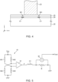
FIG. 4 is a cross-sectional view taken along the line A-A inFIG. 3 . -
FIG. 5 is a circuit diagram of themagnetic sensor 10. -
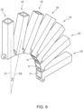
FIG. 6 is a schematic perspective view illustrating a state where themagnetic sensor array 1 is deformed. -
FIG. 7 is a schematic perspective view illustrating the outer appearance of amagnetic sensor array 2 according to a second embodiment of the present invention. -
FIG. 8 is a schematic perspective view illustrating the outer appearance of amagnetic sensor array 3 according to a third embodiment of the present invention. -
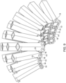
FIG. 9 is a schematic perspective view illustrating a state where themagnetic sensor array 3 is deformed. - Hereinafter, preferred embodiments of the present invention will be described in detail with reference to the accompanying drawings.
-
FIG. 1 is a schematic perspective view illustrating the outer appearance of amagnetic sensor array 1 according to a first embodiment of the present invention. - As illustrated in
FIG. 1 , themagnetic sensor array 1 according to the first embodiment has a configuration in which a plurality ofmagnetic sensors 10 each elongated in the z-direction are arranged in the x-direction. The sensitivity axis direction of each of themagnetic sensors 10 is along the z-direction. In the example illustrated inFIG. 1 , sevenmagnetic sensors 10 constitute themagnetic sensor array 1; however, the number of themagnetic sensors 10 constituting themagnetic sensor array 1 is not particularly limited to a specific number. - Each
magnetic sensor 10 includes asensor housing body 20, aconnection part 11 formed on a side surface S1 of thesensor housing body 20, and aconnection part 12 formed on a side surface S2 of thesensor housing body 20. The side surfaces S1 and S2 each constitute the yz surface and are positioned on mutually opposite sides. As illustrated inFIG. 1 , eachsensor housing body 20 has a pair ofconnection parts 12. The interval between the pair ofconnection parts 12 in the y-direction is substantially the same as or slightly smaller than the thickness of theconnection part 11 in the y-direction, and theconnection part 11 of one of themagnetic sensors 10 adjacent in the x-direction is inserted between the pair ofconnection parts 12 of the other one thereof. Then, arotary shaft 15 is inserted into through holes formed in theconnection parts connection parts rotary shaft 15. The axial direction of therotary shaft 15 is along the y-direction and does not overlap themagnetic sensor 10. The material constituting therotary shaft 15 is not particularly restricted as long as it can axially rotatably support theconnection parts rotary shaft 15 is preferably made of a non-magnetic material. -
FIG. 2 is a schematic view illustrating an example of the internal structure of themagnetic sensor 10. - As illustrated in
FIG. 2 , themagnetic sensor 10 includes asensor housing body 20 made of a non-magnetic material, asubstrate 21 housed in thesensor housing body 20, asensor chip 22, and amagnetism collector 23. Thesensor chip 22 andmagnetism collector 23 are mounted on thesubstrate 21. Themagnetism collector 23 has a rod-like shape extending in the z-direction and is made of a high permeability material such as ferrite. The xy surface of thesensor housing body 20 at which one end of themagnetism collector 23 in the z-direction is positioned constitutes a sensor head H, and thesensor chip 22 is disposed at the other end of themagnetism collector 23 in the z-direction. With this configuration, a signal magnetic field component in the z-direction emitted from an object to be measured positioned in the vicinity of the sensor head H is collected by themagnetism collector 23 to be applied to thesensor chip 22. - As described above, the
sensor housing body 20 has theconnection parts connection part 11 is formed on the side surface S1 at a portion in the vicinity of the sensor head H, and theconnection part 12 is formed on the side surface S2 at a portion in the vicinity of the sensor head H. -
FIG. 3 is a schematic plan view of thesensor chip 22, andFIG. 4 is a cross-sectional view taken along the line A-A inFIG. 3 . - As illustrated in
FIGS. 3 and4 , thesensor chip 22 has, on its element formation surface, four magnetoresistance effect elements M1 to M4 and a cancel coil C1. The cancel coil C1 is covered with aninsulating film 24, and the magnetoresistance effect elements M1 to M4 are formed on theinsulating film 24. The magnetoresistance effect elements M1 to M4 are covered with aninsulating film 25. Themagnetism collector 23 is disposed between the magnetoresistance effect elements M1, M2 and the magnetoresistance effect elements M3, M4 as viewed in the z-direction. With this configuration, a magnetic field in the z-direction collected by themagnetism collector 23 is distributed in the positive x-direction and the negative x-direction on the element formation surface of thesensor chip 22. As a result, magnetic field components in mutually opposite directions are applied to the magnetoresistance effect elements M1, M2 and magnetoresistance effect elements M3, M4. The fixed magnetization directions of the magnetoresistance effect elements M1 to M4 are made uniform in the positive x-direction or negative x-direction. - The cancel coil C1 is disposed so as to overlap the magnetoresistance effect elements M1 to M4. When a cancel current is made to flow in the cancel coil C1, cancel magnetic fields in mutually opposite directions are applied to the magnetoresistance effect elements M1, M2 and magnetoresistance effect elements M3, M4.
-
FIG. 5 is a circuit diagram of themagnetic sensor 10. - As illustrated in
FIG. 5 , the magnetoresistance effect elements M1 to M4 included in themagnetic sensor 10 are bridge-connected, and a differential signal generated thereby is supplied to adifferential amplifier 31. Thedifferential amplifier 31 generates a feedback current F1 based on the supplied differential signal. The feedback current F1 flows in the cancel coil C1. This causes the cancel coil C1 to generate a cancel magnetic field so as to make a differential signal component which is an output signal of themagnetic sensor 10 zero. The feedback current F is current-voltage converted by a resistor R, and a detection signal Vout proportional to the feedback current F is generated by avoltage measurement circuit 32 measuring the voltage across the resistor R. -
FIG. 6 is a schematic perspective view illustrating a state where themagnetic sensor array 1 according to the present embodiment is deformed. - As illustrated in
FIG. 6 , by deforming themagnetic sensor array 1 around therotary shaft 15, an angle θ between two adjacentmagnetic sensors 10 can be varied. The long dashed dotted lines Z1 and Z2 illustrated inFIG. 6 denotes the sensitivity axis directions of the respective two adjacentmagnetic sensors 10. By thus deforming themagnetic sensor array 1 constituted by the plurality ofmagnetic sensors 10 into a fan shape, a measurement surface constituted by the sensor heads H of themagnetic sensors 10 can be made into a circular-arc shape. This allows the sensor heads H of themagnetic sensors 10 to be pressed perpendicularly against even a curved surface of an object to be measured. This deformation state of themagnetic sensor array 1 can be maintained by friction force of therotary shaft 15. To reliably maintain the posture of themagnetic sensor array 1, a screw may be used as therotary shaft 15 and fixed by a nut. In this case as well, the screw and nut are preferably made of a non-magnetic material. - As described above, in the
magnetic sensor array 1 according to the present embodiment, the plurality ofmagnetic sensors 10 are connected through therotary shafts 15, thereby allowing the shape of the measurement surface constituted by the plurality of sensor heads to be varied in accordance with the surface shape of an object to be measured. -
FIG. 7 is a schematic perspective view illustrating the outer appearance of amagnetic sensor array 2 according to a second embodiment of the present invention. - As illustrated in
FIG. 7 , themagnetic sensor array 2 according to the second embodiment differs from themagnetic sensor array 1 according to the first embodiment in thatconnection parts sensor housing bodies 20 of the respectivemagnetic sensors 10 positioned at both end portions in the x-direction. Other basic configurations are the same as those of themagnetic sensor array 1 according to the first embodiment, so the same reference numerals are given to the same elements, and overlapping description will be omitted. - The
connection parts sensor housing body 20, and the positions thereof in the z-direction are the same as those of theconnection parts connection part 13 has the same shape as theconnection part 11, and theconnection part 14 has the same shape as theconnection part 12. The side surfaces S3 and S4 each constitute the xz surface and are positioned on mutually opposite sides. With this configuration, a plurality of themagnetic sensor arrays 2 according to the second embodiment can be connected in the y-direction. -
FIG. 8 is a schematic perspective view illustrating the outer appearance of amagnetic sensor array 3 according to a third embodiment of the present invention. - As illustrated in
FIG. 8 , themagnetic sensor array 3 according to the third embodiment has a configuration obtained by connecting the plurality ofmagnetic sensor arrays 2 according to the second embodiment in the y-direction. Themagnetic sensor array 3 in the example illustrated inFIG. 8 has groups G1 to G4 each having the same configuration as themagnetic sensor array 2 according to the second embodiment. Specifically, theconnection parts 13 belonging to one (e.g., group G1) of the groups adjacent in the y-direction and theconnection part 14 belonging to the other one (e.g., group G2) thereof are axially supported on each other byrotary shafts 16, whereby the groups G1 to G4 are connected in the y-direction. The axial direction of therotary shaft 16 is along the x-direction and does not overlap themagnetic sensor 10. Therotary shaft 16 can be made of the same material as therotary shaft 15. -
FIG. 9 is a schematic perspective view illustrating a state where themagnetic sensor array 3 according to the present embodiment is deformed. As illustrated inFIG. 9 , by varying the angles of themagnetic sensors 10 constituting themagnetic sensor array 3 around therotary shafts - While the preferred embodiment of the present invention has been described, the present invention is not limited to the above embodiment, and various modifications may be made within the scope of the present invention, and all such modifications are included in the present invention.
-
- 1-3
- magnetic sensor array
- 10
- magnetic sensor
- 11-14
- connection part
- 15, 16
- rotary shaft
- 20
- sensor housing body
- 21
- substrate
- 22
- sensor chip
- 23
- magnetism collector
- 24, 25
- insulating film
- 31
- differential amplifier
- 32
- voltage measurement circuit
- C1
- cancel coil
- F
- feedback current
- G1-G4
- group
- H
- sensor head
- M1-M4
- magnetoresistance effect element
- R
- resistor
- S1-S4
- side surface
Claims (5)
- A magnetic sensor array comprising a plurality of magnetic sensors,wherein each of the magnetic sensors includes a sensor chip, a sensor housing body housing the sensor chip, and first and second connection parts formed on the sensor housing body, andwherein the first connection part formed on one of adjacent magnetic sensors and the second connection part formed on other one thereof are axially supported on each other to achieve mutual connection between the plurality of magnetic sensors.
- The magnetic sensor array as claimed in claim 1,wherein the sensor housing body has a sensor head perpendicular to a sensitivity axis direction of the magnetic sensor and first and second side surfaces parallel to the sensitivity axis direction of the magnetic sensor and positioned on mutually opposite sides,wherein the first connection part is formed on the first side surface at a portion in a vicinity of the sensor head, andwherein the second connection part is formed on the second side surface at a portion in a vicinity of the sensor head.
- The magnetic sensor array as claimed in claim 2,wherein the plurality of magnetic sensors constitute a plurality of groups including first and second groups,wherein at least one of the magnetic sensors belonging to the first group further includes a third connection part formed on the sensor housing body,wherein at least one of the magnetic sensors belonging to the second group further includes a fourth connection part formed on the sensor housing body, andwherein the first and second groups are mutually connected with the third and fourth connection parts axially supported on each other.
- The magnetic sensor array as claimed in claim 3,wherein the sensor housing body further has third and fourth side surfaces parallel to the sensitivity axis direction of the magnetic sensor and perpendicular to the first and second side surfaces and are positioned on mutually opposite sides,wherein the third connection part is formed on the third side surface at a portion in a vicinity of the sensor head, andwherein the fourth connection part is formed on the fourth side surface at a portion in a vicinity of the sensor head.
- The magnetic sensor array as claimed in any one of claims 1 to 4, wherein a rotary shaft axially supporting the first and second connection parts is made of a non-magnetic material.
Applications Claiming Priority (2)
| Application Number | Priority Date | Filing Date | Title |
|---|---|---|---|
| JP2020104819A JP7468178B2 (en) | 2020-06-17 | 2020-06-17 | Magnetic Sensor Array |
| PCT/JP2021/020252 WO2021256211A1 (en) | 2020-06-17 | 2021-05-27 | Magnetic sensor array |
Publications (2)
| Publication Number | Publication Date |
|---|---|
| EP4170371A1 true EP4170371A1 (en) | 2023-04-26 |
| EP4170371A4 EP4170371A4 (en) | 2024-07-03 |
Family
ID=79197743
Family Applications (1)
| Application Number | Title | Priority Date | Filing Date |
|---|---|---|---|
| EP21825894.5A Pending EP4170371A4 (en) | 2020-06-17 | 2021-05-27 | MAGNETIC SENSOR ARRAY |
Country Status (5)
| Country | Link |
|---|---|
| US (1) | US12399235B2 (en) |
| EP (1) | EP4170371A4 (en) |
| JP (1) | JP7468178B2 (en) |
| CN (1) | CN115803646A (en) |
| WO (1) | WO2021256211A1 (en) |
Families Citing this family (2)
| Publication number | Priority date | Publication date | Assignee | Title |
|---|---|---|---|---|
| GB2643046A (en) * | 2024-07-30 | 2026-02-04 | Cerca Magnetics Ltd | Bio magnetic measuring apparatus |
| CN119880227A (en) * | 2025-03-31 | 2025-04-25 | 深圳市鑫精诚传感技术有限公司 | Sensor module |
Family Cites Families (19)
| Publication number | Priority date | Publication date | Assignee | Title |
|---|---|---|---|---|
| US3803668A (en) * | 1972-10-04 | 1974-04-16 | Electrohome Ltd | Incorporated hinge with stop and removable lock pin |
| JP2001116186A (en) * | 1999-10-19 | 2001-04-27 | Koji Yamawaki | Connectable hexagonal flat plate, connectable complex- shaped flat plate, and connecting type three-dimensional construction |
| JP2006220610A (en) * | 2005-02-14 | 2006-08-24 | Jfe Engineering Kk | Defect detection device |
| CA2743007A1 (en) | 2008-11-10 | 2010-05-14 | Pix2O Corporation | Large screen portable led display |
| JP2012508402A (en) * | 2008-11-10 | 2012-04-05 | ピックス2オー コーポレイション | Large screen portable LED display |
| US20100146734A1 (en) * | 2008-12-16 | 2010-06-17 | Munson Dennis J | Control hinge for stabilizing door |
| DE202009005546U1 (en) * | 2009-04-16 | 2009-06-18 | Igus Gmbh | cable management |
| CN103188992B (en) * | 2010-09-10 | 2016-11-16 | 柯尼卡美能达先进多层薄膜株式会社 | Biomagnetic measurement device, biomagnetic measurement system and biomagnetic measurement method |
| JP2012095939A (en) * | 2010-11-05 | 2012-05-24 | Konica Minolta Holdings Inc | Biomagnetism measurement device and method thereof |
| US10172521B2 (en) | 2013-07-08 | 2019-01-08 | General Electric Company | Systems and methods for tracking imaging attenuators |
| WO2017209273A1 (en) * | 2016-06-03 | 2017-12-07 | 国立大学法人東京医科歯科大学 | Biomagnetism measuring device |
| US11317843B2 (en) * | 2016-08-02 | 2022-05-03 | National University Corporation Tokyo Medical And Dental University | Biomagnetism measuring device |
| WO2019077865A1 (en) | 2017-10-16 | 2019-04-25 | 国立大学法人東京医科歯科大学 | Biomagnetism measurement device |
| JP2019211405A (en) * | 2018-06-07 | 2019-12-12 | Tdk株式会社 | Magnetic sensor connection body |
| JP2020003270A (en) * | 2018-06-26 | 2020-01-09 | 株式会社リコー | Atomic magnetism sensor, gradiometer, and biomagnetism measuring device |
| JP6664568B1 (en) * | 2018-08-22 | 2020-03-13 | 旭化成エレクトロニクス株式会社 | Magnetic field measuring device, magnetic field measuring method, magnetic field measuring program |
| CN110859610B (en) * | 2018-08-27 | 2023-05-05 | 中科知影(北京)科技有限公司 | Brain magnetic detection device |
| JP7286932B2 (en) * | 2018-09-08 | 2023-06-06 | Tdk株式会社 | magnetic sensor |
| JP2020168138A (en) * | 2019-04-02 | 2020-10-15 | 株式会社リコー | Magnetic measuring device and head-mounted magnetic measuring device |
-
2020
- 2020-06-17 JP JP2020104819A patent/JP7468178B2/en active Active
-
2021
- 2021-05-27 US US18/009,778 patent/US12399235B2/en active Active
- 2021-05-27 WO PCT/JP2021/020252 patent/WO2021256211A1/en not_active Ceased
- 2021-05-27 CN CN202180042058.0A patent/CN115803646A/en active Pending
- 2021-05-27 EP EP21825894.5A patent/EP4170371A4/en active Pending
Also Published As
| Publication number | Publication date |
|---|---|
| US12399235B2 (en) | 2025-08-26 |
| CN115803646A (en) | 2023-03-14 |
| EP4170371A4 (en) | 2024-07-03 |
| US20230258743A1 (en) | 2023-08-17 |
| WO2021256211A1 (en) | 2021-12-23 |
| JP2021196314A (en) | 2021-12-27 |
| JP7468178B2 (en) | 2024-04-16 |
Similar Documents
| Publication | Publication Date | Title |
|---|---|---|
| US8564283B2 (en) | Rotation-angle-detecting apparatus, rotating machine and rotation-angle-detecting method | |
| CN111065882B (en) | Anisotropic Magnetoresistive (AMR) angle sensor die with AMR angle sensor | |
| JP7284739B2 (en) | Magnetic sensor and inspection device | |
| US12399235B2 (en) | Magnetic sensor array | |
| US6556007B1 (en) | Bearing sensor having magneto resistive elements | |
| JP2009276159A (en) | Magnetic sensor | |
| EP0721563A1 (en) | Magnetoresistive linear displacement sensor, angular displacement sensor, and variable resistor | |
| JP2006003116A (en) | Magnetic sensor | |
| US20240280652A1 (en) | Magnetic sensor device | |
| CN109839231A (en) | Displacement detection type force detection structure and force sensor | |
| US20250155531A1 (en) | Magnetic sensor | |
| WO2019059284A1 (en) | Torque detection device | |
| US11892527B2 (en) | Magnetic sensor | |
| JP2021143919A (en) | Magnetic sensor and diagnosis device | |
| WO2021246289A1 (en) | Magnetic field detection device and magnetic field detection device array | |
| JP7286932B2 (en) | magnetic sensor | |
| CN106556804B (en) | Three axis micro-mechanical magnetic field sensors | |
| US11726149B2 (en) | Magnetic sensor and inspection device | |
| US11513173B2 (en) | Magnetic sensor and inspection device | |
| WO2006035350A1 (en) | Sensor | |
| US20250180678A1 (en) | Magnetic sensor | |
| EP4664135A2 (en) | Magnetic sensor and sensitivity measurement method thereof | |
| JP2004039837A (en) | Magnetic field detection element | |
| WO2001033242A1 (en) | A thin magnetoresistive current sensor system | |
| JP2018059755A (en) | Magnetic sensor unit and magnetic sensor device |
Legal Events
| Date | Code | Title | Description |
|---|---|---|---|
| STAA | Information on the status of an ep patent application or granted ep patent |
Free format text: STATUS: THE INTERNATIONAL PUBLICATION HAS BEEN MADE |
|
| PUAI | Public reference made under article 153(3) epc to a published international application that has entered the european phase |
Free format text: ORIGINAL CODE: 0009012 |
|
| STAA | Information on the status of an ep patent application or granted ep patent |
Free format text: STATUS: REQUEST FOR EXAMINATION WAS MADE |
|
| 17P | Request for examination filed |
Effective date: 20230113 |
|
| AK | Designated contracting states |
Kind code of ref document: A1 Designated state(s): AL AT BE BG CH CY CZ DE DK EE ES FI FR GB GR HR HU IE IS IT LI LT LU LV MC MK MT NL NO PL PT RO RS SE SI SK SM TR |
|
| DAV | Request for validation of the european patent (deleted) | ||
| DAX | Request for extension of the european patent (deleted) | ||
| REG | Reference to a national code |
Ref country code: DE Ref legal event code: R079 Free format text: PREVIOUS MAIN CLASS: G01R0033020000 Ipc: G01R0033000000 |
|
| A4 | Supplementary search report drawn up and despatched |
Effective date: 20240605 |
|
| RIC1 | Information provided on ipc code assigned before grant |
Ipc: G01R 33/09 20060101ALN20240529BHEP Ipc: G01R 33/00 20060101AFI20240529BHEP |