EP4170307A1 - Pressure sensor and electronic device - Google Patents
Pressure sensor and electronic device Download PDFInfo
- Publication number
- EP4170307A1 EP4170307A1 EP21854602.6A EP21854602A EP4170307A1 EP 4170307 A1 EP4170307 A1 EP 4170307A1 EP 21854602 A EP21854602 A EP 21854602A EP 4170307 A1 EP4170307 A1 EP 4170307A1
- Authority
- EP
- European Patent Office
- Prior art keywords
- sensitive adhesive
- pressure sensitive
- adhesive resistor
- resistor
- pressure
- Prior art date
- Legal status (The legal status is an assumption and is not a legal conclusion. Google has not performed a legal analysis and makes no representation as to the accuracy of the status listed.)
- Granted
Links
Images

Classifications
-
- G—PHYSICS
- G01—MEASURING; TESTING
- G01L—MEASURING FORCE, STRESS, TORQUE, WORK, MECHANICAL POWER, MECHANICAL EFFICIENCY, OR FLUID PRESSURE
- G01L1/00—Measuring force or stress, in general
- G01L1/18—Measuring force or stress, in general using properties of piezo-resistive materials, i.e. materials of which the ohmic resistance varies according to changes in magnitude or direction of force applied to the material
-
- G—PHYSICS
- G01—MEASURING; TESTING
- G01L—MEASURING FORCE, STRESS, TORQUE, WORK, MECHANICAL POWER, MECHANICAL EFFICIENCY, OR FLUID PRESSURE
- G01L1/00—Measuring force or stress, in general
- G01L1/20—Measuring force or stress, in general by measuring variations in ohmic resistance of solid materials or of electrically-conductive fluids; by making use of electrokinetic cells, i.e. liquid-containing cells wherein an electrical potential is produced or varied upon the application of stress
- G01L1/22—Measuring force or stress, in general by measuring variations in ohmic resistance of solid materials or of electrically-conductive fluids; by making use of electrokinetic cells, i.e. liquid-containing cells wherein an electrical potential is produced or varied upon the application of stress using resistance strain gauges
- G01L1/2268—Arrangements for correcting or for compensating unwanted effects
- G01L1/2281—Arrangements for correcting or for compensating unwanted effects for temperature variations
-
- G—PHYSICS
- G01—MEASURING; TESTING
- G01L—MEASURING FORCE, STRESS, TORQUE, WORK, MECHANICAL POWER, MECHANICAL EFFICIENCY, OR FLUID PRESSURE
- G01L1/00—Measuring force or stress, in general
- G01L1/20—Measuring force or stress, in general by measuring variations in ohmic resistance of solid materials or of electrically-conductive fluids; by making use of electrokinetic cells, i.e. liquid-containing cells wherein an electrical potential is produced or varied upon the application of stress
- G01L1/22—Measuring force or stress, in general by measuring variations in ohmic resistance of solid materials or of electrically-conductive fluids; by making use of electrokinetic cells, i.e. liquid-containing cells wherein an electrical potential is produced or varied upon the application of stress using resistance strain gauges
- G01L1/225—Measuring circuits therefor
- G01L1/2262—Measuring circuits therefor involving simple electrical bridges
-
- G—PHYSICS
- G01—MEASURING; TESTING
- G01L—MEASURING FORCE, STRESS, TORQUE, WORK, MECHANICAL POWER, MECHANICAL EFFICIENCY, OR FLUID PRESSURE
- G01L1/00—Measuring force or stress, in general
- G01L1/20—Measuring force or stress, in general by measuring variations in ohmic resistance of solid materials or of electrically-conductive fluids; by making use of electrokinetic cells, i.e. liquid-containing cells wherein an electrical potential is produced or varied upon the application of stress
- G01L1/22—Measuring force or stress, in general by measuring variations in ohmic resistance of solid materials or of electrically-conductive fluids; by making use of electrokinetic cells, i.e. liquid-containing cells wherein an electrical potential is produced or varied upon the application of stress using resistance strain gauges
- G01L1/2287—Measuring force or stress, in general by measuring variations in ohmic resistance of solid materials or of electrically-conductive fluids; by making use of electrokinetic cells, i.e. liquid-containing cells wherein an electrical potential is produced or varied upon the application of stress using resistance strain gauges constructional details of the strain gauges
-
- G—PHYSICS
- G01—MEASURING; TESTING
- G01L—MEASURING FORCE, STRESS, TORQUE, WORK, MECHANICAL POWER, MECHANICAL EFFICIENCY, OR FLUID PRESSURE
- G01L1/00—Measuring force or stress, in general
- G01L1/26—Auxiliary measures taken, or devices used, in connection with the measurement of force, e.g. for preventing influence of transverse components of force, for preventing overload
-
- G—PHYSICS
- G01—MEASURING; TESTING
- G01L—MEASURING FORCE, STRESS, TORQUE, WORK, MECHANICAL POWER, MECHANICAL EFFICIENCY, OR FLUID PRESSURE
- G01L5/00—Apparatus for, or methods of, measuring force, work, mechanical power, or torque, specially adapted for specific purposes
- G01L5/22—Apparatus for, or methods of, measuring force, work, mechanical power, or torque, specially adapted for specific purposes for measuring the force applied to control members, e.g. control members of vehicles, triggers
-
- H—ELECTRICITY
- H05—ELECTRIC TECHNIQUES NOT OTHERWISE PROVIDED FOR
- H05K—PRINTED CIRCUITS; CASINGS OR CONSTRUCTIONAL DETAILS OF ELECTRIC APPARATUS; MANUFACTURE OF ASSEMBLAGES OF ELECTRICAL COMPONENTS
- H05K1/00—Printed circuits
- H05K1/02—Details
- H05K1/0277—Bendability or stretchability details
-
- H—ELECTRICITY
- H05—ELECTRIC TECHNIQUES NOT OTHERWISE PROVIDED FOR
- H05K—PRINTED CIRCUITS; CASINGS OR CONSTRUCTIONAL DETAILS OF ELECTRIC APPARATUS; MANUFACTURE OF ASSEMBLAGES OF ELECTRICAL COMPONENTS
- H05K1/00—Printed circuits
- H05K1/18—Printed circuits structurally associated with non-printed electric components
- H05K1/181—Printed circuits structurally associated with non-printed electric components associated with surface mounted components
-
- H—ELECTRICITY
- H05—ELECTRIC TECHNIQUES NOT OTHERWISE PROVIDED FOR
- H05K—PRINTED CIRCUITS; CASINGS OR CONSTRUCTIONAL DETAILS OF ELECTRIC APPARATUS; MANUFACTURE OF ASSEMBLAGES OF ELECTRICAL COMPONENTS
- H05K2201/00—Indexing scheme relating to printed circuits covered by H05K1/00
- H05K2201/09—Shape and layout
- H05K2201/09209—Shape and layout details of conductors
- H05K2201/095—Conductive through-holes or vias
- H05K2201/09545—Plated through-holes or blind vias without lands
-
- H—ELECTRICITY
- H05—ELECTRIC TECHNIQUES NOT OTHERWISE PROVIDED FOR
- H05K—PRINTED CIRCUITS; CASINGS OR CONSTRUCTIONAL DETAILS OF ELECTRIC APPARATUS; MANUFACTURE OF ASSEMBLAGES OF ELECTRICAL COMPONENTS
- H05K2201/00—Indexing scheme relating to printed circuits covered by H05K1/00
- H05K2201/10—Details of components or other objects attached to or integrated in a printed circuit board
- H05K2201/10007—Types of components
- H05K2201/10022—Non-printed resistor
-
- H—ELECTRICITY
- H05—ELECTRIC TECHNIQUES NOT OTHERWISE PROVIDED FOR
- H05K—PRINTED CIRCUITS; CASINGS OR CONSTRUCTIONAL DETAILS OF ELECTRIC APPARATUS; MANUFACTURE OF ASSEMBLAGES OF ELECTRICAL COMPONENTS
- H05K2201/00—Indexing scheme relating to printed circuits covered by H05K1/00
- H05K2201/10—Details of components or other objects attached to or integrated in a printed circuit board
- H05K2201/10007—Types of components
- H05K2201/10151—Sensor
Definitions
- This application relates to the field of sensor technologies, and in particular, to a pressure sensor and an electronic device.
- a common design scheme is to use a pressure sensor as a hidden key.
- the temperature effect refers to a phenomenon that when a hot or cold housing of a smartphone is touched by a user finger or another thermostatic object, resistivity of pressure sensitive adhesive at different locations changes inconsistently due to different distances between the pressure sensitive adhesive at different locations and the finger.
- An objective of embodiments of this application is to provide a pressure sensor and an electronic device, to compensate for a signal generated by the pressure sensor due to a temperature effect, so as to guarantee measurement accuracy of the pressure sensor.
- an embodiment of this application provides a pressure sensor, including a flexible printed circuit board and multiple pressure sensitive adhesive resistors, where the multiple pressure sensitive adhesive resistors include a pressure sensitive adhesive resistor R1, a pressure sensitive adhesive resistor R2, a pressure sensitive adhesive resistor R3, a pressure sensitive adhesive resistor R4, a pressure sensitive adhesive resistor R5, and a pressure sensitive adhesive resistor R6;
- the flexible printed circuit board includes a first surface and a second surface that are opposite each other; the pressure sensitive adhesive resistor R1, the pressure sensitive adhesive resistor R3, and the pressure sensitive adhesive resistor R5 are disposed on the first surface, and the pressure sensitive adhesive resistor R2, the pressure sensitive adhesive resistor R4, and the pressure sensitive adhesive resistor R6 are disposed on the second surface;
- the flexible printed circuit board is provided with a through hole that allows the first surface to communicate with the second surface, and the through hole is at least partially covered by the pressure sensitive adhesive resistor R1, the pressure sensitive adhesive resistor R2, the pressure sensitive adhesive resistor R3, and the pressure sensitive adhesive resistor R4
- an embodiment of this application provides an electronic device, including the pressure sensor according to the first aspect, where the pressure sensor is fastened inside a device housing as a hidden key.
- multiple pressure sensitive adhesive resistors are disposed on a flexible printed circuit board.
- the multiple pressure sensitive adhesive resistors include a pressure sensitive adhesive resistor R1, a pressure sensitive adhesive resistor R2, a pressure sensitive adhesive resistor R3, a pressure sensitive adhesive resistor R4, a pressure sensitive adhesive resistor R5, and a pressure sensitive adhesive resistor R6, and the flexible printed circuit board includes a first surface and a second surface that are opposite each other.
- the pressure sensitive adhesive resistor R1, the pressure sensitive adhesive resistor R3, and the pressure sensitive adhesive resistor R5 are disposed on the first surface, and the pressure sensitive adhesive resistor R2, the pressure sensitive adhesive resistor R4, and the pressure sensitive adhesive resistor R6 are disposed on the second surface.
- the flexible printed circuit board is further provided with a through hole that allows the first surface to communicate with the second surface, and the through hole is at least partially covered by the pressure sensitive adhesive resistor R1, the pressure sensitive adhesive resistor R2, the pressure sensitive adhesive resistor R3, and the pressure sensitive adhesive resistor R4.
- the pressure sensitive adhesive resistor R1, the pressure sensitive adhesive resistor R2, the pressure sensitive adhesive resistor R5, and the pressure sensitive adhesive resistor R6 are electrically connected to form a first Wheatstone bridge, and the pressure sensitive adhesive resistor R3, the pressure sensitive adhesive resistor R4, the pressure sensitive adhesive resistor R5, and the pressure sensitive adhesive resistor R6 are electrically connected to form a second Wheatstone bridge.
- Voltage signals resulting from the temperature effect on the pressure sensitive adhesive resistor R5 and the pressure sensitive adhesive resistor R6 is used to compensate for voltage signals resulting from the temperature effect on the pressure sensitive adhesive resistor R1, the pressure sensitive adhesive resistor R2, the pressure sensitive adhesive resistor R3, and the pressure sensitive adhesive resistor R4, so that a voltage signal output by the pressure sensor includes only a voltage signal generated by the pressure action, thereby eliminating the impact of temperature on the voltage signal output by the pressure sensor, and implementing temperature compensation for the pressure sensor. This can guarantee measurement accuracy of the pressure sensor in a high or low temperature environment, and resolve problems such as false alarm or release delay of the pressure sensor caused by the temperature effect.
- FIG. 1 is a schematic diagram of a composition structure of a pressure sensor according to an embodiment of this application.
- the pressure sensor in this embodiment of this application includes a flexible printed circuit board (Flexible Printed Circuit, FPC) 110 and multiple pressure sensitive adhesive resistors. Multiple pressure sensitive adhesive resistors may be printed on the flexible printed circuit board to form a flexible printed circuit assembly (Flexible Printed Circuit Assembly, FPCA).
- the multiple pressure sensitive adhesive resistors include a pressure sensitive adhesive resistor R1, a pressure sensitive adhesive resistor R2, a pressure sensitive adhesive resistor R3, a pressure sensitive adhesive resistor R4, a pressure sensitive adhesive resistor R5, and a pressure sensitive adhesive resistor R6.
- the flexible printed circuit board 110 includes a first surface A and a second surface B that are opposite each other.
- the pressure sensitive adhesive resistor R1, the pressure sensitive adhesive resistor R3, and the pressure sensitive adhesive resistor R5 are disposed on the first surface A, and the pressure sensitive adhesive resistor R2, the pressure sensitive adhesive resistor R4, and the pressure sensitive adhesive resistor R6 are disposed on the second surface B.
- the flexible printed circuit board 110 is further provided with a through hole C that allows the first surface A to communicate with the second surface B, and the through hole C is at least partially covered by the pressure sensitive adhesive resistor R1, the pressure sensitive adhesive resistor R2, the pressure sensitive adhesive resistor R3, and the pressure sensitive adhesive resistor R4.
- the pressure sensitive adhesive resistor R1, the pressure sensitive adhesive resistor R2, the pressure sensitive adhesive resistor R5, and the pressure sensitive adhesive resistor R6 are electrically connected to form a first Wheatstone bridge, and the pressure sensitive adhesive resistor R3, the pressure sensitive adhesive resistor R4, the pressure sensitive adhesive resistor R5, and the pressure sensitive adhesive resistor R6 are electrically connected to form a second Wheatstone bridge.
- multiple pressure sensitive adhesive resistors are disposed on a flexible printed circuit board.
- the multiple pressure sensitive adhesive resistors include a pressure sensitive adhesive resistor R1, a pressure sensitive adhesive resistor R2, a pressure sensitive adhesive resistor R3, a pressure sensitive adhesive resistor R4, a pressure sensitive adhesive resistor R5, and a pressure sensitive adhesive resistor R6, and the flexible printed circuit board includes a first surface and a second surface that are opposite each other.
- the pressure sensitive adhesive resistor R1, the pressure sensitive adhesive resistor R3, and the pressure sensitive adhesive resistor R5 are disposed on the first surface, and the pressure sensitive adhesive resistor R2, the pressure sensitive adhesive resistor R4, and the pressure sensitive adhesive resistor R6 are disposed on the second surface.
- the flexible printed circuit board is further provided with a through hole that allows the first surface to communicate with the second surface, and the through hole is at least partially covered by the pressure sensitive adhesive resistor R1, the pressure sensitive adhesive resistor R2, the pressure sensitive adhesive resistor R3, and the pressure sensitive adhesive resistor R4.
- the pressure sensitive adhesive resistor R1, the pressure sensitive adhesive resistor R2, the pressure sensitive adhesive resistor R5, and the pressure sensitive adhesive resistor R6 are electrically connected to form a first Wheatstone bridge, and the pressure sensitive adhesive resistor R3, the pressure sensitive adhesive resistor R4, the pressure sensitive adhesive resistor R5, and the pressure sensitive adhesive resistor R6 are electrically connected to form a second Wheatstone bridge.
- Voltage signals resulting from the temperature effect on the pressure sensitive adhesive resistor R5 and the pressure sensitive adhesive resistor R6 is used to compensate for voltage signals resulting from the temperature effect on the pressure sensitive adhesive resistor R1, the pressure sensitive adhesive resistor R2, the pressure sensitive adhesive resistor R3, and the pressure sensitive adhesive resistor R4, so that a voltage signal output by the pressure sensor includes only a voltage signal generated by the pressure action, thereby eliminating the impact of temperature on the voltage signal output by the pressure sensor, and implementing temperature compensation for the pressure sensor. This can guarantee measurement accuracy of the pressure sensor in a high or low temperature environment, and resolve problems such as false alarm or release delay of the pressure sensor caused by the temperature effect.
- FIG. 2 is a schematic diagram of a working principle of a Wheatstone bridge in a pressure sensor according to an embodiment of this application.
- the pressure sensitive adhesive resistor R1 and the pressure sensitive adhesive resistor R2 are electrically connected, and a first voltage signal Vp11 is generated between the pressure sensitive adhesive resistor R1 and the pressure sensitive adhesive resistor R2.
- the pressure sensitive adhesive resistor R1 and the pressure sensitive adhesive resistor R2 form a bleeder circuit and are connected between a power supply VCC and a ground terminal GND, the first voltage signal Vp11 is a voltage on the pressure sensitive adhesive resistor R2.
- the pressure sensitive adhesive resistor R3 and the pressure sensitive adhesive resistor R4 are electrically connected, and a second voltage signal Vp12 is generated between the pressure sensitive adhesive resistor R3 and the pressure sensitive adhesive resistor R4. Because the pressure sensitive adhesive resistor R3 and the pressure sensitive adhesive resistor R4 form a bleeder circuit and are connected between the power supply VCC and the ground terminal GND, the second voltage signal Vp12 is a voltage on the pressure sensitive adhesive resistor R4.
- the pressure sensitive adhesive resistor R5 and the pressure sensitive adhesive resistor R6 are electrically connected, and a third voltage signal Vp13 is generated between the pressure sensitive adhesive resistor R5 and the pressure sensitive adhesive resistor R6.
- the third voltage signal Vp13 is a voltage on the pressure sensitive adhesive resistor R6.
- the first voltage signal Vp11 that is, the voltage on the pressure sensitive adhesive resistor R2
- the second voltage signal Vp12 that is, the voltage on the pressure sensitive adhesive resistor R4
- the third voltage signal Vp13 that is, the voltage on the pressure sensitive adhesive resistor R6, is a voltage generated through voltage division of the pressure sensitive adhesive resistor R5 and the pressure sensitive adhesive resistor R6.
- the first voltage signal Vp11 that is, the voltage on the pressure sensitive adhesive resistor R2
- the second voltage signal Vp12 that is, the voltage on the pressure sensitive adhesive resistor R4
- the third voltage signal Vp13 that is, the voltage on the pressure sensitive adhesive resistor R6, is a voltage generated through voltage division of the pressure sensitive adhesive resistor R5 and the pressure sensitive adhesive resistor R6.
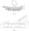
- the pressure sensitive adhesive resistor R1, the pressure sensitive adhesive resistor R2, the pressure sensitive adhesive resistor R3, and the pressure sensitive adhesive resistor R4 at least partially cover the through hole C, that is, are in a region of the flexible printed circuit board subjected to the action of pressure, a curvature of such region changes under the action of pressure, as shown in FIG. 3 .
- the pressure sensitive adhesive resistor R1 and the pressure sensitive adhesive resistor R3 are squeezed, and the pressure sensitive adhesive resistor R2 and the pressure sensitive adhesive resistor R4 are stretched, so that resistivities of the pressure sensitive adhesive resistor R1 and the pressure sensitive adhesive resistor R3 decrease, and resistivities of the pressure sensitive adhesive resistor R2 and the pressure sensitive adhesive resistor R4 increase.
- the pressure sensitive adhesive resistor R1, the pressure sensitive adhesive resistor R2, the pressure sensitive adhesive resistor R3, and the pressure sensitive adhesive resistor R4 are affected by the pressure action, so that a voltage generated due to voltage division of the pressure sensitive adhesive resistor R1 and the pressure sensitive adhesive resistor R3 decreases and a voltage generated due to voltage division of the pressure sensitive adhesive resistor R2 and the pressure sensitive adhesive resistor R4 increases. Because the pressure sensitive adhesive resistor R5 and the pressure sensitive adhesive resistor R6 do not cover the through hole C, that is, are located in a region of the flexible printed circuit board not subjected to the action of pressure, a curvature of such region does not change under the action of pressure, as shown in FIG. 3 .
- the pressure sensitive adhesive resistor R5 and the pressure sensitive adhesive resistor R6 are not squeezed or stretched, and resistivities of the pressure sensitive adhesive resistor R5 and the pressure sensitive adhesive resistor R6 do not change.
- the pressure sensitive adhesive resistor R5 and the pressure sensitive adhesive resistor R6 are free from the action of pressure, and a voltage generated due to voltage division of the pressure sensitive adhesive resistor R5 and pressure sensitive adhesive resistor R6 does not change.
- both the ratio of the pressure sensitive adhesive resistor R1 to the pressure sensitive adhesive resistor R2 and the ratio of the pressure sensitive adhesive resistor R3 to the pressure sensitive adhesive resistor R4 are equal to the ratio of the pressure sensitive adhesive resistor R5 to the pressure sensitive adhesive resistor R6. Therefore, after being subjected to the action of pressure, the voltages generated due to the voltage division of the pressure sensitive adhesive resistor R2 and pressure sensitive adhesive resistor R4 both are greater than the voltage generated due to the voltage division of the pressure sensitive adhesive resistor R6, that is, Vp11 > Vp13, and Vp12 > Vp13.
- the pressure sensor converts the pressure received into an electrical signal for output.
- the first voltage signal Vp11 that is, the voltage on the pressure sensitive adhesive resistor R2
- the second voltage signal Vp12 that is, the voltage on the pressure sensitive adhesive resistor R4
- the third voltage signal Vp 13, that is, the voltage on the pressure sensitive adhesive resistor R6, is a voltage generated through voltage division of the pressure sensitive adhesive resistor R5 and the pressure sensitive adhesive resistor R6.
- the resistivities of the pressure sensitive adhesive resistor R1, the pressure sensitive adhesive resistor R2, the pressure sensitive adhesive resistor R3, the pressure sensitive adhesive resistor R4, the pressure sensitive adhesive resistor R5, and the pressure sensitive adhesive resistor R6 increase as the ambient temperature rises.
- the pressure sensitive adhesive resistor R1, the pressure sensitive adhesive resistor R3, and the pressure sensitive adhesive resistor R5 are closer to the user finger than the pressure sensitive adhesive resistor R2, the pressure sensitive adhesive resistor R4, and the pressure sensitive adhesive resistor R6, temperatures of the pressure sensitive adhesive resistor R1, the pressure sensitive adhesive resistor R3, and the pressure sensitive adhesive resistor R5 are lower than temperatures of the pressure sensitive adhesive resistor R2, the pressure sensitive adhesive resistor R4, and the pressure sensitive adhesive resistor R6, and resistivities of the pressure sensitive adhesive resistor R1, the pressure sensitive adhesive resistor R3, and the pressure sensitive adhesive resistor R5 are lower than resistivities of the pressure sensitive adhesive resistor R2, the pressure sensitive adhesive resistor R4, and the pressure sensitive adhesive resistor R6.
- the pressure sensitive adhesive resistor R1, the pressure sensitive adhesive resistor R2, the pressure sensitive adhesive resistor R3, the pressure sensitive adhesive resistor R4, the pressure sensitive adhesive resistor R5, and the pressure sensitive adhesive resistor R6 are affected by the temperature effect, so that voltages generated due to voltage division of the pressure sensitive adhesive resistor R1, the pressure sensitive adhesive resistor R3, and the pressure sensitive adhesive resistor R5 decrease, and voltages generated due to the voltage division of the pressure sensitive adhesive resistor R2, the pressure sensitive adhesive resistor R4, and the pressure sensitive adhesive resistor R6 increase.
- a distance between the pressure sensitive adhesive resistor R5 and the pressure sensitive adhesive resistor R1 and a distance between the pressure sensitive adhesive resistor R5 and the pressure sensitive adhesive resistor R3 are less than a preset threshold
- a distance between the pressure sensitive adhesive resistor R6 and the pressure sensitive adhesive resistor R2 and a distance between the pressure sensitive adhesive resistor R6 and the pressure sensitive adhesive resistor R4 are less than the preset threshold.
- the temperature of the pressure sensitive adhesive resistor R5 keeps consistent with the temperatures of the pressure sensitive adhesive resistor R1 and the pressure sensitive adhesive resistor R3 under any condition
- the temperature of the pressure sensitive adhesive resistor R6 keeps consistent with the temperatures of the pressure sensitive adhesive resistor R2 and the pressure sensitive adhesive resistor R4 under any condition. Therefore, under the influence of the temperature effect, the decrements of the voltages generated due to the voltage division of the pressure sensitive adhesive resistor R1, the pressure sensitive adhesive resistor R3, and the pressure sensitive adhesive resistor R5 are equal; and increments of the voltages generated due to the voltage division of the pressure sensitive adhesive resistor R2, the pressure sensitive adhesive resistor R4, and the pressure sensitive adhesive resistor R6 are equal.
- the preset threshold may be determined based on volume or the like of the pressure sensitive adhesive resistor, which is not limited in this embodiment of this application.
- ⁇ U1 Vp11 - Vp 13.
- FIG. 4 is a schematic diagram of another composition structure of a pressure sensor according to an embodiment of this application.
- the pressure sensor in this embodiment of this application includes a flexible printed circuit board 110 and multiple pressure sensitive adhesive resistors.
- the multiple pressure sensitive adhesive resistors include a pressure sensitive adhesive resistor R1, a pressure sensitive adhesive resistor R2, a pressure sensitive adhesive resistor R3, a pressure sensitive adhesive resistor R4, a pressure sensitive adhesive resistor R5, and a pressure sensitive adhesive resistor R6.
- the flexible printed circuit board 110 includes a first surface A and a second surface B that are opposite each other.
- the pressure sensitive adhesive resistor R1, the pressure sensitive adhesive resistor R3, and the pressure sensitive adhesive resistor R5 are disposed on the first surface A, and the pressure sensitive adhesive resistor R2, the pressure sensitive adhesive resistor R4, and the pressure sensitive adhesive resistor R6 are disposed on the second surface B.
- the flexible printed circuit board 110 is further provided with through holes that allow the first surface A to communicate with the second surface B.
- the through holes include a first through hole D and a second through hole E.
- the first through hole D is at least partially covered by the pressure sensitive adhesive resistor R1 and the pressure sensitive adhesive resistor R2, and the second through hole E is at least partially covered by the pressure sensitive adhesive resistor R3 and the pressure sensitive adhesive resistor R4.
- the pressure sensitive adhesive resistor R1, the pressure sensitive adhesive resistor R2, the pressure sensitive adhesive resistor R5, and the pressure sensitive adhesive resistor R6 are electrically connected to form a first Wheatstone bridge, and the pressure sensitive adhesive resistor R3, the pressure sensitive adhesive resistor R4, the pressure sensitive adhesive resistor R5, and the pressure sensitive adhesive resistor R6 are electrically connected to form a second Wheatstone bridge.
- the Wheatstone bridge in the pressure sensor in this embodiment works in the same way as the Wheatstone bridge in the pressure sensor in FIG. 1 . Therefore, details are not described herein again.
- an embodiment of this application further provides an electronic device.
- the electronic device includes the pressure sensor in the foregoing embodiments.
- the electronic device may be at least one of a mobile phone, a tablet computer, an in-vehicle computer, a wearable device, an intelligent robot, and the like.
- a type of the electronic device is not limited in this embodiment of this application.
- the pressure sensor is fastened inside a device housing 210 as a hidden key.
- the device housing 210 is a metal housing, and the pressure sensor is fastened inside the device housing 210 by using a double-sided adhesive 220.
- multiple pressure sensitive adhesive resistors are disposed on a flexible printed circuit board.
- the multiple pressure sensitive adhesive resistors include a pressure sensitive adhesive resistor R1, a pressure sensitive adhesive resistor R2, a pressure sensitive adhesive resistor R3, a pressure sensitive adhesive resistor R4, a pressure sensitive adhesive resistor R5, and a pressure sensitive adhesive resistor R6, and the flexible printed circuit board includes a first surface and a second surface that are opposite each other.
- the pressure sensitive adhesive resistor R1, the pressure sensitive adhesive resistor R3, and the pressure sensitive adhesive resistor R5 are disposed on the first surface, and the pressure sensitive adhesive resistor R2, the pressure sensitive adhesive resistor R4, and the pressure sensitive adhesive resistor R6 are disposed on the second surface.
- the flexible printed circuit board is further provided with a through hole that allows the first surface to communicate with the second surface, and the through hole is at least partially covered by the pressure sensitive adhesive resistor R1, the pressure sensitive adhesive resistor R2, the pressure sensitive adhesive resistor R3, and the pressure sensitive adhesive resistor R4.
- the pressure sensitive adhesive resistor R1, the pressure sensitive adhesive resistor R2, the pressure sensitive adhesive resistor R5, and the pressure sensitive adhesive resistor R6 are electrically connected to form a first Wheatstone bridge, and the pressure sensitive adhesive resistor R3, the pressure sensitive adhesive resistor R4, the pressure sensitive adhesive resistor R5, and the pressure sensitive adhesive resistor R6 are electrically connected to form a second Wheatstone bridge.
- Voltage signals resulting from the temperature effect on the pressure sensitive adhesive resistor R5 and the pressure sensitive adhesive resistor R6 is used to compensate for voltage signals resulting from the temperature effect on the pressure sensitive adhesive resistor R1, the pressure sensitive adhesive resistor R2, the pressure sensitive adhesive resistor R3, and the pressure sensitive adhesive resistor R4, so that a voltage signal output by the pressure sensor includes only the voltage signal generated by the pressure action, thereby eliminating the impact of temperature on the voltage signal output by the pressure sensor, and implementing temperature compensation for the pressure sensor. This can guarantee measurement accuracy of the pressure sensor in a high or low temperature environment, and resolve problems such as false alarm or release delay of the pressure sensor caused by the temperature effect.
- the method in the foregoing embodiments may be implemented by software in addition to a necessary universal hardware platform or by hardware only. In most cases, the former is a more preferred implementation.
- the technical solutions of this application essentially, or the part contributing to the prior art may be implemented in a form of a software product.
- the software product is stored in a storage medium (for example, ROM/RAM, a magnetic disk, or an optical disc), and includes several instructions for instructing a terminal (which may be a mobile phone, a computer, a server, an air conditioner, a network device, or the like) to perform the method described in the embodiments of this application.
Landscapes
- Physics & Mathematics (AREA)
- General Physics & Mathematics (AREA)
- Engineering & Computer Science (AREA)
- Microelectronics & Electronic Packaging (AREA)
- Measuring Fluid Pressure (AREA)
- Force Measurement Appropriate To Specific Purposes (AREA)
Abstract
Description
- The present invention claims priority to
Chinese Patent Application No. 202010788347.2, filed with the China National Intellectual Property Administration on August 7, 2020 - This application relates to the field of sensor technologies, and in particular, to a pressure sensor and an electronic device.
- With increasing requirements on product appearance, a design of hidden keys is increasingly present on flagship and high-end smartphones. A common design scheme is to use a pressure sensor as a hidden key.
- In the design scheme in which a pressure sensor is used as a hidden key, generally pressure sensitive adhesive resistors are used to form a Wheatstone bridge, so as to convert the pressure received into a voltage difference for output. Resistivity of the pressure sensitive adhesive resistor changes with temperature. In a case that a smartphone stays in a high or low temperature environment for a long time, for example, the smartphone has been placed outdoor in the sunlight in summer, or the smartphone has been placed outdoor in a low temperature in winter, after a user picks up the smartphone and presses the hidden key, although the user's finger has been lifted, the pressure sensitive adhesive resistor of the hidden key still generates and outputs a voltage difference due to a temperature effect. As a result, the smartphone considers that the user presses and holds the hidden key without releasing it, which in turn leads to a problem that the smartphone is switched off or does not respond to the user's another press on the hidden key.
- In this application, the temperature effect refers to a phenomenon that when a hot or cold housing of a smartphone is touched by a user finger or another thermostatic object, resistivity of pressure sensitive adhesive at different locations changes inconsistently due to different distances between the pressure sensitive adhesive at different locations and the finger.
- An objective of embodiments of this application is to provide a pressure sensor and an electronic device, to compensate for a signal generated by the pressure sensor due to a temperature effect, so as to guarantee measurement accuracy of the pressure sensor.
- According to a first aspect, an embodiment of this application provides a pressure sensor, including a flexible printed circuit board and multiple pressure sensitive adhesive resistors, where the multiple pressure sensitive adhesive resistors include a pressure sensitive adhesive resistor R1, a pressure sensitive adhesive resistor R2, a pressure sensitive adhesive resistor R3, a pressure sensitive adhesive resistor R4, a pressure sensitive adhesive resistor R5, and a pressure sensitive adhesive resistor R6; the flexible printed circuit board includes a first surface and a second surface that are opposite each other; the pressure sensitive adhesive resistor R1, the pressure sensitive adhesive resistor R3, and the pressure sensitive adhesive resistor R5 are disposed on the first surface, and the pressure sensitive adhesive resistor R2, the pressure sensitive adhesive resistor R4, and the pressure sensitive adhesive resistor R6 are disposed on the second surface; the flexible printed circuit board is provided with a through hole that allows the first surface to communicate with the second surface, and the through hole is at least partially covered by the pressure sensitive adhesive resistor R1, the pressure sensitive adhesive resistor R2, the pressure sensitive adhesive resistor R3, and the pressure sensitive adhesive resistor R4; and the pressure sensitive adhesive resistor R1, the pressure sensitive adhesive resistor R2, the pressure sensitive adhesive resistor R5, and the pressure sensitive adhesive resistor R6 are electrically connected to form a first Wheatstone bridge, and the pressure sensitive adhesive resistor R3, the pressure sensitive adhesive resistor R4, the pressure sensitive adhesive resistor R5, and the pressure sensitive adhesive resistor R6 are electrically connected to form a second Wheatstone bridge.
- According to a second aspect, an embodiment of this application provides an electronic device, including the pressure sensor according to the first aspect, where the pressure sensor is fastened inside a device housing as a hidden key.
- According to the pressure sensor and electronic device provided in the embodiments of this application, multiple pressure sensitive adhesive resistors are disposed on a flexible printed circuit board. The multiple pressure sensitive adhesive resistors include a pressure sensitive adhesive resistor R1, a pressure sensitive adhesive resistor R2, a pressure sensitive adhesive resistor R3, a pressure sensitive adhesive resistor R4, a pressure sensitive adhesive resistor R5, and a pressure sensitive adhesive resistor R6, and the flexible printed circuit board includes a first surface and a second surface that are opposite each other. The pressure sensitive adhesive resistor R1, the pressure sensitive adhesive resistor R3, and the pressure sensitive adhesive resistor R5 are disposed on the first surface, and the pressure sensitive adhesive resistor R2, the pressure sensitive adhesive resistor R4, and the pressure sensitive adhesive resistor R6 are disposed on the second surface. The flexible printed circuit board is further provided with a through hole that allows the first surface to communicate with the second surface, and the through hole is at least partially covered by the pressure sensitive adhesive resistor R1, the pressure sensitive adhesive resistor R2, the pressure sensitive adhesive resistor R3, and the pressure sensitive adhesive resistor R4. The pressure sensitive adhesive resistor R1, the pressure sensitive adhesive resistor R2, the pressure sensitive adhesive resistor R5, and the pressure sensitive adhesive resistor R6 are electrically connected to form a first Wheatstone bridge, and the pressure sensitive adhesive resistor R3, the pressure sensitive adhesive resistor R4, the pressure sensitive adhesive resistor R5, and the pressure sensitive adhesive resistor R6 are electrically connected to form a second Wheatstone bridge. Voltage signals resulting from the temperature effect on the pressure sensitive adhesive resistor R5 and the pressure sensitive adhesive resistor R6 is used to compensate for voltage signals resulting from the temperature effect on the pressure sensitive adhesive resistor R1, the pressure sensitive adhesive resistor R2, the pressure sensitive adhesive resistor R3, and the pressure sensitive adhesive resistor R4, so that a voltage signal output by the pressure sensor includes only a voltage signal generated by the pressure action, thereby eliminating the impact of temperature on the voltage signal output by the pressure sensor, and implementing temperature compensation for the pressure sensor. This can guarantee measurement accuracy of the pressure sensor in a high or low temperature environment, and resolve problems such as false alarm or release delay of the pressure sensor caused by the temperature effect.
- The drawings described herein are intended for a further understanding of this application and constitute a part of this application. Example embodiments of this application and descriptions thereof are intended to explain this application, and do not constitute any inappropriate limitation on this application. In the accompanying drawings:
-
FIG. 1 is a schematic diagram of a composition structure of a pressure sensor according to an embodiment of this application; -
FIG. 2 is a schematic diagram of a working principle of a Wheatstone bridge in a pressure sensor according to an embodiment of this application; -
FIG. 3 is a schematic diagram of a pressure action on a pressure sensor according to an embodiment of this application; and -
FIG. 4 is a schematic diagram of another composition structure of a pressure sensor according to an embodiment of this application. - The following clearly and completely describes the technical solutions in the embodiments of this application with reference to the accompanying drawings in the embodiments of this application. Apparently, the described embodiments are some but not all of the embodiments of this application. All other embodiments obtained by a person of ordinary skill in the art based on the embodiments of this application without creative efforts shall fall within the protection scope of this application.
-
FIG. 1 is a schematic diagram of a composition structure of a pressure sensor according to an embodiment of this application. As shown inFIG. 1 , the pressure sensor in this embodiment of this application includes a flexible printed circuit board (Flexible Printed Circuit, FPC) 110 and multiple pressure sensitive adhesive resistors. Multiple pressure sensitive adhesive resistors may be printed on the flexible printed circuit board to form a flexible printed circuit assembly (Flexible Printed Circuit Assembly, FPCA). The multiple pressure sensitive adhesive resistors include a pressure sensitive adhesive resistor R1, a pressure sensitive adhesive resistor R2, a pressure sensitive adhesive resistor R3, a pressure sensitive adhesive resistor R4, a pressure sensitive adhesive resistor R5, and a pressure sensitive adhesive resistor R6. The flexible printedcircuit board 110 includes a first surface A and a second surface B that are opposite each other. The pressure sensitive adhesive resistor R1, the pressure sensitive adhesive resistor R3, and the pressure sensitive adhesive resistor R5 are disposed on the first surface A, and the pressure sensitive adhesive resistor R2, the pressure sensitive adhesive resistor R4, and the pressure sensitive adhesive resistor R6 are disposed on the second surface B. The flexible printedcircuit board 110 is further provided with a through hole C that allows the first surface A to communicate with the second surface B, and the through hole C is at least partially covered by the pressure sensitive adhesive resistor R1, the pressure sensitive adhesive resistor R2, the pressure sensitive adhesive resistor R3, and the pressure sensitive adhesive resistor R4. The pressure sensitive adhesive resistor R1, the pressure sensitive adhesive resistor R2, the pressure sensitive adhesive resistor R5, and the pressure sensitive adhesive resistor R6 are electrically connected to form a first Wheatstone bridge, and the pressure sensitive adhesive resistor R3, the pressure sensitive adhesive resistor R4, the pressure sensitive adhesive resistor R5, and the pressure sensitive adhesive resistor R6 are electrically connected to form a second Wheatstone bridge. - In the pressure sensor provided in this embodiment of this application, multiple pressure sensitive adhesive resistors are disposed on a flexible printed circuit board. The multiple pressure sensitive adhesive resistors include a pressure sensitive adhesive resistor R1, a pressure sensitive adhesive resistor R2, a pressure sensitive adhesive resistor R3, a pressure sensitive adhesive resistor R4, a pressure sensitive adhesive resistor R5, and a pressure sensitive adhesive resistor R6, and the flexible printed circuit board includes a first surface and a second surface that are opposite each other. The pressure sensitive adhesive resistor R1, the pressure sensitive adhesive resistor R3, and the pressure sensitive adhesive resistor R5 are disposed on the first surface, and the pressure sensitive adhesive resistor R2, the pressure sensitive adhesive resistor R4, and the pressure sensitive adhesive resistor R6 are disposed on the second surface. The flexible printed circuit board is further provided with a through hole that allows the first surface to communicate with the second surface, and the through hole is at least partially covered by the pressure sensitive adhesive resistor R1, the pressure sensitive adhesive resistor R2, the pressure sensitive adhesive resistor R3, and the pressure sensitive adhesive resistor R4. The pressure sensitive adhesive resistor R1, the pressure sensitive adhesive resistor R2, the pressure sensitive adhesive resistor R5, and the pressure sensitive adhesive resistor R6 are electrically connected to form a first Wheatstone bridge, and the pressure sensitive adhesive resistor R3, the pressure sensitive adhesive resistor R4, the pressure sensitive adhesive resistor R5, and the pressure sensitive adhesive resistor R6 are electrically connected to form a second Wheatstone bridge. Voltage signals resulting from the temperature effect on the pressure sensitive adhesive resistor R5 and the pressure sensitive adhesive resistor R6 is used to compensate for voltage signals resulting from the temperature effect on the pressure sensitive adhesive resistor R1, the pressure sensitive adhesive resistor R2, the pressure sensitive adhesive resistor R3, and the pressure sensitive adhesive resistor R4, so that a voltage signal output by the pressure sensor includes only a voltage signal generated by the pressure action, thereby eliminating the impact of temperature on the voltage signal output by the pressure sensor, and implementing temperature compensation for the pressure sensor. This can guarantee measurement accuracy of the pressure sensor in a high or low temperature environment, and resolve problems such as false alarm or release delay of the pressure sensor caused by the temperature effect.
- The following describes a working principle of the pressure sensor according to the embodiments of this application with reference to
FIG. 2 to FIG. 3 . -
FIG. 2 is a schematic diagram of a working principle of a Wheatstone bridge in a pressure sensor according to an embodiment of this application. As shown inFIG. 2 , the pressure sensitive adhesive resistor R1 and the pressure sensitive adhesive resistor R2 are electrically connected, and a first voltage signal Vp11 is generated between the pressure sensitive adhesive resistor R1 and the pressure sensitive adhesive resistor R2. Because the pressure sensitive adhesive resistor R1 and the pressure sensitive adhesive resistor R2 form a bleeder circuit and are connected between a power supply VCC and a ground terminal GND, the first voltage signal Vp11 is a voltage on the pressure sensitive adhesive resistor R2. The pressure sensitive adhesive resistor R3 and the pressure sensitive adhesive resistor R4 are electrically connected, and a second voltage signal Vp12 is generated between the pressure sensitive adhesive resistor R3 and the pressure sensitive adhesive resistor R4. Because the pressure sensitive adhesive resistor R3 and the pressure sensitive adhesive resistor R4 form a bleeder circuit and are connected between the power supply VCC and the ground terminal GND, the second voltage signal Vp12 is a voltage on the pressure sensitive adhesive resistor R4. The pressure sensitive adhesive resistor R5 and the pressure sensitive adhesive resistor R6 are electrically connected, and a third voltage signal Vp13 is generated between the pressure sensitive adhesive resistor R5 and the pressure sensitive adhesive resistor R6. Because the pressure sensitive adhesive resistor R5 and the pressure sensitive adhesive resistor R6 form a bleeder circuit and are connected between the power supply VCC and the ground terminal GND, the third voltage signal Vp13 is a voltage on the pressure sensitive adhesive resistor R6. A signal △U1 output by the first Wheatstone bridge is a difference between the first voltage signal Vp11 and the third voltage signal Vp13, that is, △U1 = Vp11 - Vp13. A signal ΔU2 output by the second Wheatstone bridge is a difference between the second voltage signal Vp12 and the third voltage signal Vp13, that is, △U2 = Vp12 - Vp13. A signal △U output by the pressure sensor is a sum of the signal △U1 output by the first Wheatstone bridge and the signal △U2 output by the second Wheatstone bridge, that is, △U = △U1 + △U2. - In a case that the pressure sensor in this embodiment of this application is not affected by the pressure action and temperature effect, the first voltage signal Vp11, that is, the voltage on the pressure sensitive adhesive resistor R2, is a voltage generated through voltage division of the pressure sensitive adhesive resistor R1 and the pressure sensitive adhesive resistor R2. The second voltage signal Vp12, that is, the voltage on the pressure sensitive adhesive resistor R4, is a voltage generated through voltage division of the pressure sensitive adhesive resistor R3 and the pressure sensitive adhesive resistor R4. The third voltage signal Vp13, that is, the voltage on the pressure sensitive adhesive resistor R6, is a voltage generated through voltage division of the pressure sensitive adhesive resistor R5 and the pressure sensitive adhesive resistor R6. Because a ratio of the pressure sensitive adhesive resistor R1 to the pressure sensitive adhesive resistor R2, a ratio of the pressure sensitive adhesive resistor R3 to the pressure sensitive adhesive resistor R4, and a ratio of the pressure sensitive adhesive resistor R5 to the pressure sensitive adhesive resistor R6 are equal, voltages generated due to voltage division of the pressure sensitive adhesive resistor R2, the pressure sensitive adhesive resistor R4, and the pressure sensitive adhesive resistor R6 are equal, that is, Vp11 = Vp12 = Vp13. In this case, the voltage signal output by the first Wheatstone bridge is △U1 = Vp11 - Vp13 = 0, the voltage signal output by the second Wheatstone bridge is ΔU2 = Vp12 - Vp13 = 0, and the voltage signal finally output by the pressure sensor is △U = △U1 + △U2 = 0, so the pressure sensor outputs no signal.
- In a case that the pressure sensor in this embodiment of this application is affected by the pressure action but not affected by the temperature effect, the first voltage signal Vp11, that is, the voltage on the pressure sensitive adhesive resistor R2, is a voltage generated through voltage division of the pressure sensitive adhesive resistor R1 and the pressure sensitive adhesive resistor R2; the second voltage signal Vp12, that is, the voltage on the pressure sensitive adhesive resistor R4, is a voltage generated through voltage division of the pressure sensitive adhesive resistor R3 and the pressure sensitive adhesive resistor R4; and the third voltage signal Vp13, that is, the voltage on the pressure sensitive adhesive resistor R6, is a voltage generated through voltage division of the pressure sensitive adhesive resistor R5 and the pressure sensitive adhesive resistor R6. Because the pressure sensitive adhesive resistor R1, the pressure sensitive adhesive resistor R2, the pressure sensitive adhesive resistor R3, and the pressure sensitive adhesive resistor R4 at least partially cover the through hole C, that is, are in a region of the flexible printed circuit board subjected to the action of pressure, a curvature of such region changes under the action of pressure, as shown in
FIG. 3 . Therefore, as the curvature of the region of the flexible printed circuit board subjected to the action of pressure changes, the pressure sensitive adhesive resistor R1 and the pressure sensitive adhesive resistor R3 are squeezed, and the pressure sensitive adhesive resistor R2 and the pressure sensitive adhesive resistor R4 are stretched, so that resistivities of the pressure sensitive adhesive resistor R1 and the pressure sensitive adhesive resistor R3 decrease, and resistivities of the pressure sensitive adhesive resistor R2 and the pressure sensitive adhesive resistor R4 increase. The pressure sensitive adhesive resistor R1, the pressure sensitive adhesive resistor R2, the pressure sensitive adhesive resistor R3, and the pressure sensitive adhesive resistor R4 are affected by the pressure action, so that a voltage generated due to voltage division of the pressure sensitive adhesive resistor R1 and the pressure sensitive adhesive resistor R3 decreases and a voltage generated due to voltage division of the pressure sensitive adhesive resistor R2 and the pressure sensitive adhesive resistor R4 increases. Because the pressure sensitive adhesive resistor R5 and the pressure sensitive adhesive resistor R6 do not cover the through hole C, that is, are located in a region of the flexible printed circuit board not subjected to the action of pressure, a curvature of such region does not change under the action of pressure, as shown inFIG. 3 . Therefore, the pressure sensitive adhesive resistor R5 and the pressure sensitive adhesive resistor R6 are not squeezed or stretched, and resistivities of the pressure sensitive adhesive resistor R5 and the pressure sensitive adhesive resistor R6 do not change. The pressure sensitive adhesive resistor R5 and the pressure sensitive adhesive resistor R6 are free from the action of pressure, and a voltage generated due to voltage division of the pressure sensitive adhesive resistor R5 and pressure sensitive adhesive resistor R6 does not change. - In addition, before being subjected to the action of pressure, both the ratio of the pressure sensitive adhesive resistor R1 to the pressure sensitive adhesive resistor R2 and the ratio of the pressure sensitive adhesive resistor R3 to the pressure sensitive adhesive resistor R4 are equal to the ratio of the pressure sensitive adhesive resistor R5 to the pressure sensitive adhesive resistor R6. Therefore, after being subjected to the action of pressure, the voltages generated due to the voltage division of the pressure sensitive adhesive resistor R2 and pressure sensitive adhesive resistor R4 both are greater than the voltage generated due to the voltage division of the pressure sensitive adhesive resistor R6, that is, Vp11 > Vp13, and Vp12 > Vp13. In this case, the voltage signal output by the first Wheatstone bridge, △U1 = Vp11 - Vp13 > 0, is an electrical signal generated due to pressure on the first Wheatstone bridge, the voltage signal output by the second Wheatstone bridge, ΔU2 = Vp12 - Vp13 > 0, is an electrical signal generated due to pressure on the second Wheatstone bridge, and the voltage signal finally output by the pressure sensor is △U = △U1 + △U2 > 0. The pressure sensor converts the pressure received into an electrical signal for output.
- In a case that the pressure sensor in this embodiment of this application is affected by the pressure action and the temperature effect, the first voltage signal Vp11, that is, the voltage on the pressure sensitive adhesive resistor R2, is a voltage generated through voltage division of the pressure sensitive adhesive resistor R1 and the pressure sensitive adhesive resistor R2; the second voltage signal Vp12, that is, the voltage on the pressure sensitive adhesive resistor R4, is a voltage generated through voltage division of the pressure sensitive adhesive resistor R3 and the pressure sensitive adhesive resistor R4; and the third voltage signal Vp 13, that is, the voltage on the pressure sensitive adhesive resistor R6, is a voltage generated through voltage division of the pressure sensitive adhesive resistor R5 and the pressure sensitive adhesive resistor R6. In a case that the pressure sensor is in a high-temperature environment for a long time, the resistivities of the pressure sensitive adhesive resistor R1, the pressure sensitive adhesive resistor R2, the pressure sensitive adhesive resistor R3, the pressure sensitive adhesive resistor R4, the pressure sensitive adhesive resistor R5, and the pressure sensitive adhesive resistor R6 increase as the ambient temperature rises. When a user finger that has a temperature lower than the ambient temperature presses the pressure sensor, as shown in
FIG. 4 , because the pressure sensitive adhesive resistor R1, the pressure sensitive adhesive resistor R3, and the pressure sensitive adhesive resistor R5 are closer to the user finger than the pressure sensitive adhesive resistor R2, the pressure sensitive adhesive resistor R4, and the pressure sensitive adhesive resistor R6, temperatures of the pressure sensitive adhesive resistor R1, the pressure sensitive adhesive resistor R3, and the pressure sensitive adhesive resistor R5 are lower than temperatures of the pressure sensitive adhesive resistor R2, the pressure sensitive adhesive resistor R4, and the pressure sensitive adhesive resistor R6, and resistivities of the pressure sensitive adhesive resistor R1, the pressure sensitive adhesive resistor R3, and the pressure sensitive adhesive resistor R5 are lower than resistivities of the pressure sensitive adhesive resistor R2, the pressure sensitive adhesive resistor R4, and the pressure sensitive adhesive resistor R6. The pressure sensitive adhesive resistor R1, the pressure sensitive adhesive resistor R2, the pressure sensitive adhesive resistor R3, the pressure sensitive adhesive resistor R4, the pressure sensitive adhesive resistor R5, and the pressure sensitive adhesive resistor R6 are affected by the temperature effect, so that voltages generated due to voltage division of the pressure sensitive adhesive resistor R1, the pressure sensitive adhesive resistor R3, and the pressure sensitive adhesive resistor R5 decrease, and voltages generated due to the voltage division of the pressure sensitive adhesive resistor R2, the pressure sensitive adhesive resistor R4, and the pressure sensitive adhesive resistor R6 increase. - In addition, a distance between the pressure sensitive adhesive resistor R5 and the pressure sensitive adhesive resistor R1 and a distance between the pressure sensitive adhesive resistor R5 and the pressure sensitive adhesive resistor R3 are less than a preset threshold, and a distance between the pressure sensitive adhesive resistor R6 and the pressure sensitive adhesive resistor R2 and a distance between the pressure sensitive adhesive resistor R6 and the pressure sensitive adhesive resistor R4 are less than the preset threshold. In this case, it may be considered that the temperature of the pressure sensitive adhesive resistor R5 keeps consistent with the temperatures of the pressure sensitive adhesive resistor R1 and the pressure sensitive adhesive resistor R3 under any condition, and the temperature of the pressure sensitive adhesive resistor R6 keeps consistent with the temperatures of the pressure sensitive adhesive resistor R2 and the pressure sensitive adhesive resistor R4 under any condition. Therefore, under the influence of the temperature effect, the decrements of the voltages generated due to the voltage division of the pressure sensitive adhesive resistor R1, the pressure sensitive adhesive resistor R3, and the pressure sensitive adhesive resistor R5 are equal; and increments of the voltages generated due to the voltage division of the pressure sensitive adhesive resistor R2, the pressure sensitive adhesive resistor R4, and the pressure sensitive adhesive resistor R6 are equal. The preset threshold may be determined based on volume or the like of the pressure sensitive adhesive resistor, which is not limited in this embodiment of this application.
- In this case, the voltage signal output by the first Wheatstone bridge is △U1 = Vp11 - Vp 13. Through the temperature-effect-induced increment of the voltage generated due to the voltage division of the pressure sensitive adhesive resistor R6, the temperature-effect-induced increment of the voltage generated due to the voltage division of the pressure sensitive adhesive resistor R2 is removed, so that △U1 includes only the electrical signal generated by the first Wheatstone bridge under pressure. The voltage signal output by the second Wheatstone bridge is ΔU2 = Vp12 - Vp13. Through the temperature-effect-induced increment of the voltage generated due to the voltage division of the pressure sensitive adhesive resistor R6, the temperature-effect-induced increment of the voltage generated due to the voltage division of the pressure sensitive adhesive resistor R4 is removed, so that ΔU2 includes only the electrical signal generated by the second Wheatstone bridge under pressure. In this way, the voltage signal finally output by the pressure sensor, △U = △U1 + ΔU2, is only an electrical signal converted by the pressure sensor from the pressure received.
-
FIG. 4 is a schematic diagram of another composition structure of a pressure sensor according to an embodiment of this application. As shown inFIG. 4 , the pressure sensor in this embodiment of this application includes a flexible printedcircuit board 110 and multiple pressure sensitive adhesive resistors. The multiple pressure sensitive adhesive resistors include a pressure sensitive adhesive resistor R1, a pressure sensitive adhesive resistor R2, a pressure sensitive adhesive resistor R3, a pressure sensitive adhesive resistor R4, a pressure sensitive adhesive resistor R5, and a pressure sensitive adhesive resistor R6. The flexible printedcircuit board 110 includes a first surface A and a second surface B that are opposite each other. The pressure sensitive adhesive resistor R1, the pressure sensitive adhesive resistor R3, and the pressure sensitive adhesive resistor R5 are disposed on the first surface A, and the pressure sensitive adhesive resistor R2, the pressure sensitive adhesive resistor R4, and the pressure sensitive adhesive resistor R6 are disposed on the second surface B. The flexible printedcircuit board 110 is further provided with through holes that allow the first surface A to communicate with the second surface B. The through holes include a first through hole D and a second through hole E. The first through hole D is at least partially covered by the pressure sensitive adhesive resistor R1 and the pressure sensitive adhesive resistor R2, and the second through hole E is at least partially covered by the pressure sensitive adhesive resistor R3 and the pressure sensitive adhesive resistor R4. The pressure sensitive adhesive resistor R1, the pressure sensitive adhesive resistor R2, the pressure sensitive adhesive resistor R5, and the pressure sensitive adhesive resistor R6 are electrically connected to form a first Wheatstone bridge, and the pressure sensitive adhesive resistor R3, the pressure sensitive adhesive resistor R4, the pressure sensitive adhesive resistor R5, and the pressure sensitive adhesive resistor R6 are electrically connected to form a second Wheatstone bridge. The Wheatstone bridge in the pressure sensor in this embodiment works in the same way as the Wheatstone bridge in the pressure sensor inFIG. 1 . Therefore, details are not described herein again. - Based on a same technical concept, an embodiment of this application further provides an electronic device. The electronic device includes the pressure sensor in the foregoing embodiments. The electronic device may be at least one of a mobile phone, a tablet computer, an in-vehicle computer, a wearable device, an intelligent robot, and the like. A type of the electronic device is not limited in this embodiment of this application. As shown in
FIG. 3 , in the electronic device, the pressure sensor is fastened inside adevice housing 210 as a hidden key. In some optional examples, thedevice housing 210 is a metal housing, and the pressure sensor is fastened inside thedevice housing 210 by using a double-sided adhesive 220. - In the electronic device according to this embodiment of this application, multiple pressure sensitive adhesive resistors are disposed on a flexible printed circuit board. The multiple pressure sensitive adhesive resistors include a pressure sensitive adhesive resistor R1, a pressure sensitive adhesive resistor R2, a pressure sensitive adhesive resistor R3, a pressure sensitive adhesive resistor R4, a pressure sensitive adhesive resistor R5, and a pressure sensitive adhesive resistor R6, and the flexible printed circuit board includes a first surface and a second surface that are opposite each other. The pressure sensitive adhesive resistor R1, the pressure sensitive adhesive resistor R3, and the pressure sensitive adhesive resistor R5 are disposed on the first surface, and the pressure sensitive adhesive resistor R2, the pressure sensitive adhesive resistor R4, and the pressure sensitive adhesive resistor R6 are disposed on the second surface. The flexible printed circuit board is further provided with a through hole that allows the first surface to communicate with the second surface, and the through hole is at least partially covered by the pressure sensitive adhesive resistor R1, the pressure sensitive adhesive resistor R2, the pressure sensitive adhesive resistor R3, and the pressure sensitive adhesive resistor R4. The pressure sensitive adhesive resistor R1, the pressure sensitive adhesive resistor R2, the pressure sensitive adhesive resistor R5, and the pressure sensitive adhesive resistor R6 are electrically connected to form a first Wheatstone bridge, and the pressure sensitive adhesive resistor R3, the pressure sensitive adhesive resistor R4, the pressure sensitive adhesive resistor R5, and the pressure sensitive adhesive resistor R6 are electrically connected to form a second Wheatstone bridge. Voltage signals resulting from the temperature effect on the pressure sensitive adhesive resistor R5 and the pressure sensitive adhesive resistor R6 is used to compensate for voltage signals resulting from the temperature effect on the pressure sensitive adhesive resistor R1, the pressure sensitive adhesive resistor R2, the pressure sensitive adhesive resistor R3, and the pressure sensitive adhesive resistor R4, so that a voltage signal output by the pressure sensor includes only the voltage signal generated by the pressure action, thereby eliminating the impact of temperature on the voltage signal output by the pressure sensor, and implementing temperature compensation for the pressure sensor. This can guarantee measurement accuracy of the pressure sensor in a high or low temperature environment, and resolve problems such as false alarm or release delay of the pressure sensor caused by the temperature effect.
- It should be noted that, in this specification, the terms "include", "comprise", or any of their variants are intended to cover a non-exclusive inclusion, so that a process, a method, an article, or an apparatus that includes a series of elements not only includes those elements but also includes other elements that are not expressly listed, or further includes elements inherent to such a process, method, article, or apparatus. In absence of more constraints, an element preceded by "includes a..." does not preclude the existence of other identical elements in the process, method, article, or apparatus that includes the element.
- According to the description of the foregoing implementations, persons skilled in the art can clearly understand that the method in the foregoing embodiments may be implemented by software in addition to a necessary universal hardware platform or by hardware only. In most cases, the former is a more preferred implementation. Based on such an understanding, the technical solutions of this application essentially, or the part contributing to the prior art may be implemented in a form of a software product. The software product is stored in a storage medium (for example, ROM/RAM, a magnetic disk, or an optical disc), and includes several instructions for instructing a terminal (which may be a mobile phone, a computer, a server, an air conditioner, a network device, or the like) to perform the method described in the embodiments of this application.
- The embodiments of this application are described above with reference to the accompanying drawings, but this application is not limited to the foregoing implementations. The foregoing implementations are only illustrative rather than restrictive. Inspired by this application, persons of ordinary skill in the art can still derive many variations without departing from the essence of this application and the protection scope of the claims. All these variations shall fall within the protection of this application.
Claims (8)
- A pressure sensor, comprising a flexible printed circuit board and multiple pressure sensitive adhesive resistors, wherein the multiple pressure sensitive adhesive resistors comprise a pressure sensitive adhesive resistor R1, a pressure sensitive adhesive resistor R2, a pressure sensitive adhesive resistor R3, a pressure sensitive adhesive resistor R4, a pressure sensitive adhesive resistor R5, and a pressure sensitive adhesive resistor R6;the flexible printed circuit board comprises a first surface and a second surface that are opposite each other;the pressure sensitive adhesive resistor R1, the pressure sensitive adhesive resistor R3, and the pressure sensitive adhesive resistor R5 are disposed on the first surface, and the pressure sensitive adhesive resistor R2, the pressure sensitive adhesive resistor R4, and the pressure sensitive adhesive resistor R6 are disposed on the second surface;the flexible printed circuit board is provided with a through hole that allows the first surface to communicate with the second surface, and the through hole is at least partially covered by the pressure sensitive adhesive resistor R1, the pressure sensitive adhesive resistor R2, the pressure sensitive adhesive resistor R3, and the pressure sensitive adhesive resistor R4; andthe pressure sensitive adhesive resistor R1, the pressure sensitive adhesive resistor R2, the pressure sensitive adhesive resistor R5, and the pressure sensitive adhesive resistor R6 are electrically connected to form a first Wheatstone bridge, and the pressure sensitive adhesive resistor R3, the pressure sensitive adhesive resistor R4, the pressure sensitive adhesive resistor R5, and the pressure sensitive adhesive resistor R6 are electrically connected to form a second Wheatstone bridge.
- The pressure sensor according to claim 1, wherein a ratio of the pressure sensitive adhesive resistor R1 to the pressure sensitive adhesive resistor R2, a ratio of the pressure sensitive adhesive resistor R3 to the pressure sensitive adhesive resistor R4, and a ratio of the pressure sensitive adhesive resistor R5 to the pressure sensitive adhesive resistor R6 are equal.
- The pressure sensor according to claim 2, wherein the pressure sensitive adhesive resistor R1 and the pressure sensitive adhesive resistor R2 are electrically connected, and a first voltage signal is generated between the pressure sensitive adhesive resistor R1 and the pressure sensitive adhesive resistor R2;the pressure sensitive adhesive resistor R3 and the pressure sensitive adhesive resistor R4 are electrically connected, and a second voltage signal is generated between the pressure sensitive adhesive resistor R3 and the pressure sensitive adhesive resistor R4;the pressure sensitive adhesive resistor R5 and the pressure sensitive adhesive resistor R6 are electrically connected, and a third voltage signal is generated between the pressure sensitive adhesive resistor R5 and the pressure sensitive adhesive resistor R6; anda signal output by the first Wheatstone bridge is a difference between the first voltage signal and the third voltage signal; a signal output by the second Wheatstone bridge is a difference between the second voltage signal and the third voltage signal; and a signal output by the pressure sensor is a sum of the signal output by the first Wheatstone bridge and the signal output by the second Wheatstone bridge.
- The pressure sensor according to any one of claims 1 to 3, wherein a distance between the pressure sensitive adhesive resistor R5 and the pressure sensitive adhesive resistor R1 and a distance between the pressure sensitive adhesive resistor R5 and the pressure sensitive adhesive resistor R3 are less than a preset threshold, so that temperature of the pressure sensitive adhesive resistor R5 is consistent with temperature of the pressure sensitive adhesive resistor R1 and temperature of the pressure sensitive adhesive resistor R3; and a distance between the pressure sensitive adhesive resistor R6 and the pressure sensitive adhesive resistor R2 and a distance between the pressure sensitive adhesive resistor R6 and the pressure sensitive adhesive resistor R4 are less than the preset threshold, so that temperature of the pressure sensitive adhesive resistor R6 is consistent with temperature of the pressure sensitive adhesive resistor R2 and temperature of the pressure sensitive adhesive resistor R4.
- The pressure sensor according to claim 4, wherein the through hole comprises a first through hole and a second through hole, the first through hole is at least partially covered by the pressure sensitive adhesive resistor R1 and the pressure sensitive adhesive resistor R2, and the second through hole is at least partially covered by the pressure sensitive adhesive resistor R3 and the pressure sensitive adhesive resistor R4.
- An electronic device, comprising the pressure sensor according to any one of claims 1 to 5, wherein the pressure sensor is fastened inside a device housing as a hidden key.
- The electronic device according to claim 6, wherein the device housing is a metal housing, and the pressure sensor is fastened inside the device housing by using a double-sided adhesive.
- The electronic device according to claim 7, wherein the electronic device comprises at least one of the following: a mobile phone, a tablet computer, an in-vehicle computer, a wearable device, and an intelligent robot.
Applications Claiming Priority (2)
| Application Number | Priority Date | Filing Date | Title |
|---|---|---|---|
| CN202010788347.2A CN111998976B (en) | 2020-08-07 | 2020-08-07 | Pressure sensor and electronic device |
| PCT/CN2021/110833 WO2022028525A1 (en) | 2020-08-07 | 2021-08-05 | Pressure sensor and electronic device |
Publications (3)
| Publication Number | Publication Date |
|---|---|
| EP4170307A1 true EP4170307A1 (en) | 2023-04-26 |
| EP4170307A4 EP4170307A4 (en) | 2023-12-13 |
| EP4170307B1 EP4170307B1 (en) | 2024-11-06 |
Family
ID=73462364
Family Applications (1)
| Application Number | Title | Priority Date | Filing Date |
|---|---|---|---|
| EP21854602.6A Active EP4170307B1 (en) | 2020-08-07 | 2021-08-05 | Pressure sensor and electronic device |
Country Status (6)
| Country | Link |
|---|---|
| US (1) | US12326374B2 (en) |
| EP (1) | EP4170307B1 (en) |
| JP (1) | JP7493095B2 (en) |
| CN (1) | CN111998976B (en) |
| ES (1) | ES2997546T3 (en) |
| WO (1) | WO2022028525A1 (en) |
Families Citing this family (5)
| Publication number | Priority date | Publication date | Assignee | Title |
|---|---|---|---|---|
| CN111998976B (en) * | 2020-08-07 | 2022-03-25 | 维沃移动通信有限公司 | Pressure sensor and electronic device |
| CN112860114B (en) * | 2021-02-24 | 2023-11-03 | 维沃移动通信有限公司 | A pressure-sensitive module and electronic device |
| JP7766412B2 (en) * | 2021-04-22 | 2025-11-10 | 株式会社日立製作所 | Pressure sensor device, method for manufacturing pressure sensor device, work management system, and method for manufacturing glove |
| CN113282192A (en) | 2021-05-24 | 2021-08-20 | 维沃移动通信有限公司 | Pressure-sensitive module and electronic equipment |
| CN113411078B (en) * | 2021-06-07 | 2024-10-29 | 维沃移动通信有限公司 | Key module and electronic equipment |
Family Cites Families (14)
| Publication number | Priority date | Publication date | Assignee | Title |
|---|---|---|---|---|
| US3102420A (en) * | 1960-08-05 | 1963-09-03 | Bell Telephone Labor Inc | High strain non-linearity compensation of semiconductive sensing members |
| GB2107876B (en) * | 1981-10-01 | 1985-08-14 | Itt Ind Ltd | Temperature compensation of strain gauges |
| JPH0739975B2 (en) * | 1990-02-28 | 1995-05-01 | 工業技術院長 | Distributed tactile sensor |
| FR2741951B1 (en) | 1995-12-04 | 1998-02-20 | Europ Propulsion | WHEATSTONE BRIDGE WITH GRADIENT TEMPERATURE COMPENSATION BETWEEN MAIN BRIDGE RESISTORS AND APPLICATION TO A PRESSURE SENSOR WITH EXTENSOMETRIC GAUGES |
| CN204856438U (en) | 2015-09-01 | 2015-12-09 | 宸鸿科技(厦门)有限公司 | Pressure sensing input module |
| WO2017133017A1 (en) * | 2016-02-06 | 2017-08-10 | 深圳纽迪瑞科技开发有限公司 | Pressure sensor, electronic device, and method for manufacturing pressure sensor |
| WO2017133016A1 (en) * | 2016-02-06 | 2017-08-10 | 深圳纽迪瑞科技开发有限公司 | Pressure sensor, electronic device, and method for manufacturing pressure sensor |
| WO2018133054A1 (en) * | 2017-01-21 | 2018-07-26 | 深圳纽迪瑞科技开发有限公司 | Pressure-sensing structure, and electronic product |
| WO2018145304A1 (en) * | 2017-02-10 | 2018-08-16 | 深圳市汇顶科技股份有限公司 | Piezoresistive sensor, pressure measurement device and electronic device |
| CN107797702B (en) * | 2017-10-20 | 2021-02-26 | 厦门天马微电子有限公司 | Pressure sensor, display panel and display device |
| CN208653681U (en) | 2018-06-15 | 2019-03-26 | 深圳纽迪瑞科技开发有限公司 | Pressure sensitive component and electronic equipment |
| CN110823446B (en) * | 2019-10-18 | 2022-01-07 | 成都凯天电子股份有限公司 | Secondary temperature compensation zero debugging method for silicon piezoresistive pressure sensor |
| CN111426413A (en) * | 2020-05-15 | 2020-07-17 | 罕王微电子(辽宁)有限公司 | Novel pressure sensor and design method |
| CN111998976B (en) * | 2020-08-07 | 2022-03-25 | 维沃移动通信有限公司 | Pressure sensor and electronic device |
-
2020
- 2020-08-07 CN CN202010788347.2A patent/CN111998976B/en active Active
-
2021
- 2021-08-05 WO PCT/CN2021/110833 patent/WO2022028525A1/en not_active Ceased
- 2021-08-05 JP JP2023507448A patent/JP7493095B2/en active Active
- 2021-08-05 EP EP21854602.6A patent/EP4170307B1/en active Active
- 2021-08-05 ES ES21854602T patent/ES2997546T3/en active Active
-
2023
- 2023-02-02 US US18/105,195 patent/US12326374B2/en active Active
Also Published As
| Publication number | Publication date |
|---|---|
| JP2023536199A (en) | 2023-08-23 |
| ES2997546T3 (en) | 2025-02-17 |
| CN111998976A (en) | 2020-11-27 |
| EP4170307B1 (en) | 2024-11-06 |
| JP7493095B2 (en) | 2024-05-30 |
| US12326374B2 (en) | 2025-06-10 |
| US20230184604A1 (en) | 2023-06-15 |
| WO2022028525A1 (en) | 2022-02-10 |
| CN111998976B (en) | 2022-03-25 |
| EP4170307A4 (en) | 2023-12-13 |
Similar Documents
| Publication | Publication Date | Title |
|---|---|---|
| US12326374B2 (en) | Pressure sensor and electronic device | |
| WO2018026192A1 (en) | Electronic device comprising force sensor | |
| EP2487564B1 (en) | Apparatus and method for calibrating a tactile force sensing surface | |
| CN110174961B (en) | Mobile terminal | |
| CN111459330B (en) | Electronic equipment and pressure key operation method | |
| CN110764644A (en) | Electronic device and pressure compensation method | |
| CN109378878B (en) | Charging circuit, charging processing method, electronic device, and storage medium | |
| CN110597411A (en) | Pressure detection circuit, electronic device, and control method for pressure detection circuit | |
| WO2022242601A1 (en) | Electronic device | |
| US11913846B2 (en) | Force sensing systems | |
| CN115061597B (en) | Touch display modules and electronic devices | |
| CN110672262B (en) | Pressure key threshold calibration method, device, storage medium and electronic device | |
| CN113110762A (en) | Touch display device and false touch prevention method thereof | |
| CN108595105A (en) | Light supplement lamp control method and device, storage medium and electronic equipment | |
| CN114740996B (en) | Signal acquisition method and electronic equipment | |
| WO2023071980A1 (en) | Pressure sensing control method and apparatus for electronic device, and electronic device and medium | |
| US20250274369A1 (en) | Master/slave node determination method and apparatus, and electronic device and storage medium | |
| CN2938609Y (en) | Mobile phone with infrared thermometer | |
| CN117294787A (en) | Electronic equipment | |
| CN206639200U (en) | Display device and electronic equipment with pressure sensitivity function | |
| CN109510259A (en) | Charging circuit, charging method, electronic equipment and storage medium | |
| CN110021981B (en) | Charger and terminal | |
| CN217718729U (en) | Fingerprint identification device and terminal equipment | |
| CN110209543A (en) | A kind of detection method and terminal of earphone socket | |
| JPS6168626A (en) | Image input/output device |
Legal Events
| Date | Code | Title | Description |
|---|---|---|---|
| STAA | Information on the status of an ep patent application or granted ep patent |
Free format text: STATUS: THE INTERNATIONAL PUBLICATION HAS BEEN MADE |
|
| PUAI | Public reference made under article 153(3) epc to a published international application that has entered the european phase |
Free format text: ORIGINAL CODE: 0009012 |
|
| STAA | Information on the status of an ep patent application or granted ep patent |
Free format text: STATUS: REQUEST FOR EXAMINATION WAS MADE |
|
| 17P | Request for examination filed |
Effective date: 20230119 |
|
| AK | Designated contracting states |
Kind code of ref document: A1 Designated state(s): AL AT BE BG CH CY CZ DE DK EE ES FI FR GB GR HR HU IE IS IT LI LT LU LV MC MK MT NL NO PL PT RO RS SE SI SK SM TR |
|
| DAV | Request for validation of the european patent (deleted) | ||
| DAX | Request for extension of the european patent (deleted) | ||
| A4 | Supplementary search report drawn up and despatched |
Effective date: 20231113 |
|
| RIC1 | Information provided on ipc code assigned before grant |
Ipc: G01L 1/26 20060101ALI20231107BHEP Ipc: G01L 1/22 20060101ALI20231107BHEP Ipc: G01L 1/18 20060101AFI20231107BHEP |
|
| GRAP | Despatch of communication of intention to grant a patent |
Free format text: ORIGINAL CODE: EPIDOSNIGR1 |
|
| STAA | Information on the status of an ep patent application or granted ep patent |
Free format text: STATUS: GRANT OF PATENT IS INTENDED |
|
| INTG | Intention to grant announced |
Effective date: 20240716 |
|
| RIC1 | Information provided on ipc code assigned before grant |
Ipc: G01L 1/26 20060101ALI20240705BHEP Ipc: G01L 1/22 20060101ALI20240705BHEP Ipc: G01L 1/18 20060101AFI20240705BHEP |
|
| GRAS | Grant fee paid |
Free format text: ORIGINAL CODE: EPIDOSNIGR3 |
|
| GRAA | (expected) grant |
Free format text: ORIGINAL CODE: 0009210 |
|
| STAA | Information on the status of an ep patent application or granted ep patent |
Free format text: STATUS: THE PATENT HAS BEEN GRANTED |
|
| AK | Designated contracting states |
Kind code of ref document: B1 Designated state(s): AL AT BE BG CH CY CZ DE DK EE ES FI FR GB GR HR HU IE IS IT LI LT LU LV MC MK MT NL NO PL PT RO RS SE SI SK SM TR |
|
| REG | Reference to a national code |
Ref country code: GB Ref legal event code: FG4D |
|
| REG | Reference to a national code |
Ref country code: CH Ref legal event code: EP |
|
| REG | Reference to a national code |
Ref country code: DE Ref legal event code: R096 Ref document number: 602021021613 Country of ref document: DE |
|
| REG | Reference to a national code |
Ref country code: IE Ref legal event code: FG4D |
|
| REG | Reference to a national code |
Ref country code: NL Ref legal event code: FP |
|
| REG | Reference to a national code |
Ref country code: ES Ref legal event code: FG2A Ref document number: 2997546 Country of ref document: ES Kind code of ref document: T3 Effective date: 20250217 |
|
| REG | Reference to a national code |
Ref country code: LT Ref legal event code: MG9D |
|
| PG25 | Lapsed in a contracting state [announced via postgrant information from national office to epo] |
Ref country code: IS Free format text: LAPSE BECAUSE OF FAILURE TO SUBMIT A TRANSLATION OF THE DESCRIPTION OR TO PAY THE FEE WITHIN THE PRESCRIBED TIME-LIMIT Effective date: 20250306 Ref country code: HR Free format text: LAPSE BECAUSE OF FAILURE TO SUBMIT A TRANSLATION OF THE DESCRIPTION OR TO PAY THE FEE WITHIN THE PRESCRIBED TIME-LIMIT Effective date: 20241106 Ref country code: PT Free format text: LAPSE BECAUSE OF FAILURE TO SUBMIT A TRANSLATION OF THE DESCRIPTION OR TO PAY THE FEE WITHIN THE PRESCRIBED TIME-LIMIT Effective date: 20250306 |
|
| PG25 | Lapsed in a contracting state [announced via postgrant information from national office to epo] |
Ref country code: FI Free format text: LAPSE BECAUSE OF FAILURE TO SUBMIT A TRANSLATION OF THE DESCRIPTION OR TO PAY THE FEE WITHIN THE PRESCRIBED TIME-LIMIT Effective date: 20241106 |
|
| REG | Reference to a national code |
Ref country code: AT Ref legal event code: MK05 Ref document number: 1739815 Country of ref document: AT Kind code of ref document: T Effective date: 20241106 |
|
| PG25 | Lapsed in a contracting state [announced via postgrant information from national office to epo] |
Ref country code: BG Free format text: LAPSE BECAUSE OF FAILURE TO SUBMIT A TRANSLATION OF THE DESCRIPTION OR TO PAY THE FEE WITHIN THE PRESCRIBED TIME-LIMIT Effective date: 20241106 |
|
| PG25 | Lapsed in a contracting state [announced via postgrant information from national office to epo] |
Ref country code: NO Free format text: LAPSE BECAUSE OF FAILURE TO SUBMIT A TRANSLATION OF THE DESCRIPTION OR TO PAY THE FEE WITHIN THE PRESCRIBED TIME-LIMIT Effective date: 20250206 |
|
| PG25 | Lapsed in a contracting state [announced via postgrant information from national office to epo] |
Ref country code: LV Free format text: LAPSE BECAUSE OF FAILURE TO SUBMIT A TRANSLATION OF THE DESCRIPTION OR TO PAY THE FEE WITHIN THE PRESCRIBED TIME-LIMIT Effective date: 20241106 Ref country code: GR Free format text: LAPSE BECAUSE OF FAILURE TO SUBMIT A TRANSLATION OF THE DESCRIPTION OR TO PAY THE FEE WITHIN THE PRESCRIBED TIME-LIMIT Effective date: 20250207 Ref country code: AT Free format text: LAPSE BECAUSE OF FAILURE TO SUBMIT A TRANSLATION OF THE DESCRIPTION OR TO PAY THE FEE WITHIN THE PRESCRIBED TIME-LIMIT Effective date: 20241106 |
|
| PG25 | Lapsed in a contracting state [announced via postgrant information from national office to epo] |
Ref country code: PL Free format text: LAPSE BECAUSE OF FAILURE TO SUBMIT A TRANSLATION OF THE DESCRIPTION OR TO PAY THE FEE WITHIN THE PRESCRIBED TIME-LIMIT Effective date: 20241106 |
|
| PG25 | Lapsed in a contracting state [announced via postgrant information from national office to epo] |
Ref country code: RS Free format text: LAPSE BECAUSE OF FAILURE TO SUBMIT A TRANSLATION OF THE DESCRIPTION OR TO PAY THE FEE WITHIN THE PRESCRIBED TIME-LIMIT Effective date: 20250206 |
|
| PG25 | Lapsed in a contracting state [announced via postgrant information from national office to epo] |
Ref country code: SM Free format text: LAPSE BECAUSE OF FAILURE TO SUBMIT A TRANSLATION OF THE DESCRIPTION OR TO PAY THE FEE WITHIN THE PRESCRIBED TIME-LIMIT Effective date: 20241106 |
|
| PG25 | Lapsed in a contracting state [announced via postgrant information from national office to epo] |
Ref country code: DK Free format text: LAPSE BECAUSE OF FAILURE TO SUBMIT A TRANSLATION OF THE DESCRIPTION OR TO PAY THE FEE WITHIN THE PRESCRIBED TIME-LIMIT Effective date: 20241106 |
|
| PGFP | Annual fee paid to national office [announced via postgrant information from national office to epo] |
Ref country code: GB Payment date: 20250626 Year of fee payment: 5 |
|
| PG25 | Lapsed in a contracting state [announced via postgrant information from national office to epo] |
Ref country code: EE Free format text: LAPSE BECAUSE OF FAILURE TO SUBMIT A TRANSLATION OF THE DESCRIPTION OR TO PAY THE FEE WITHIN THE PRESCRIBED TIME-LIMIT Effective date: 20241106 |
|
| PG25 | Lapsed in a contracting state [announced via postgrant information from national office to epo] |
Ref country code: RO Free format text: LAPSE BECAUSE OF FAILURE TO SUBMIT A TRANSLATION OF THE DESCRIPTION OR TO PAY THE FEE WITHIN THE PRESCRIBED TIME-LIMIT Effective date: 20241106 |
|
| PG25 | Lapsed in a contracting state [announced via postgrant information from national office to epo] |
Ref country code: SK Free format text: LAPSE BECAUSE OF FAILURE TO SUBMIT A TRANSLATION OF THE DESCRIPTION OR TO PAY THE FEE WITHIN THE PRESCRIBED TIME-LIMIT Effective date: 20241106 |
|
| PG25 | Lapsed in a contracting state [announced via postgrant information from national office to epo] |
Ref country code: CZ Free format text: LAPSE BECAUSE OF FAILURE TO SUBMIT A TRANSLATION OF THE DESCRIPTION OR TO PAY THE FEE WITHIN THE PRESCRIBED TIME-LIMIT Effective date: 20241106 |
|
| REG | Reference to a national code |
Ref country code: DE Ref legal event code: R097 Ref document number: 602021021613 Country of ref document: DE |
|
| PGFP | Annual fee paid to national office [announced via postgrant information from national office to epo] |
Ref country code: NL Payment date: 20250704 Year of fee payment: 5 |
|
| PG25 | Lapsed in a contracting state [announced via postgrant information from national office to epo] |
Ref country code: SE Free format text: LAPSE BECAUSE OF FAILURE TO SUBMIT A TRANSLATION OF THE DESCRIPTION OR TO PAY THE FEE WITHIN THE PRESCRIBED TIME-LIMIT Effective date: 20241106 |
|
| PLBE | No opposition filed within time limit |
Free format text: ORIGINAL CODE: 0009261 |
|
| STAA | Information on the status of an ep patent application or granted ep patent |
Free format text: STATUS: NO OPPOSITION FILED WITHIN TIME LIMIT |
|
| PGFP | Annual fee paid to national office [announced via postgrant information from national office to epo] |
Ref country code: ES Payment date: 20250905 Year of fee payment: 5 |
|
| PGFP | Annual fee paid to national office [announced via postgrant information from national office to epo] |
Ref country code: DE Payment date: 20250702 Year of fee payment: 5 |
|
| 26N | No opposition filed |
Effective date: 20250807 |
|
| PGFP | Annual fee paid to national office [announced via postgrant information from national office to epo] |
Ref country code: IT Payment date: 20250722 Year of fee payment: 5 |
|
| PGFP | Annual fee paid to national office [announced via postgrant information from national office to epo] |
Ref country code: FR Payment date: 20250703 Year of fee payment: 5 |
|
| REG | Reference to a national code |
Ref country code: CH Ref legal event code: H13 Free format text: ST27 STATUS EVENT CODE: U-0-0-H10-H13 (AS PROVIDED BY THE NATIONAL OFFICE) Effective date: 20260324 |
|
| PG25 | Lapsed in a contracting state [announced via postgrant information from national office to epo] |
Ref country code: MC Free format text: LAPSE BECAUSE OF FAILURE TO SUBMIT A TRANSLATION OF THE DESCRIPTION OR TO PAY THE FEE WITHIN THE PRESCRIBED TIME-LIMIT Effective date: 20241106 |
|
| PG25 | Lapsed in a contracting state [announced via postgrant information from national office to epo] |
Ref country code: LU Free format text: LAPSE BECAUSE OF NON-PAYMENT OF DUE FEES Effective date: 20250805 |
|
| PG25 | Lapsed in a contracting state [announced via postgrant information from national office to epo] |
Ref country code: CH Free format text: LAPSE BECAUSE OF NON-PAYMENT OF DUE FEES Effective date: 20250831 |