EP4167488A1 - Poly phase filter with phase error enhance technique - Google Patents
Poly phase filter with phase error enhance technique Download PDFInfo
- Publication number
- EP4167488A1 EP4167488A1 EP22190376.8A EP22190376A EP4167488A1 EP 4167488 A1 EP4167488 A1 EP 4167488A1 EP 22190376 A EP22190376 A EP 22190376A EP 4167488 A1 EP4167488 A1 EP 4167488A1
- Authority
- EP
- European Patent Office
- Prior art keywords
- clock signal
- signal
- input signal
- adjustable delay
- delay circuit
- Prior art date
- Legal status (The legal status is an assumption and is not a legal conclusion. Google has not performed a legal analysis and makes no representation as to the accuracy of the status listed.)
- Pending
Links
Images

Classifications
-
- H—ELECTRICITY
- H03—ELECTRONIC CIRCUITRY
- H03L—AUTOMATIC CONTROL, STARTING, SYNCHRONISATION OR STABILISATION OF GENERATORS OF ELECTRONIC OSCILLATIONS OR PULSES
- H03L7/00—Automatic control of frequency or phase; Synchronisation
- H03L7/06—Automatic control of frequency or phase; Synchronisation using a reference signal applied to a frequency- or phase-locked loop
- H03L7/08—Details of the phase-locked loop
- H03L7/081—Details of the phase-locked loop provided with an additional controlled phase shifter
- H03L7/0812—Details of the phase-locked loop provided with an additional controlled phase shifter and where no voltage or current controlled oscillator is used
-
- H—ELECTRICITY
- H03—ELECTRONIC CIRCUITRY
- H03K—PULSE TECHNIQUE
- H03K5/00—Manipulating of pulses not covered by one of the other main groups of this subclass
- H03K5/13—Arrangements having a single output and transforming input signals into pulses delivered at desired time intervals
- H03K5/135—Arrangements having a single output and transforming input signals into pulses delivered at desired time intervals by the use of time reference signals, e.g. clock signals
-
- H—ELECTRICITY
- H03—ELECTRONIC CIRCUITRY
- H03B—GENERATION OF OSCILLATIONS, DIRECTLY OR BY FREQUENCY-CHANGING, BY CIRCUITS EMPLOYING ACTIVE ELEMENTS WHICH OPERATE IN A NON-SWITCHING MANNER; GENERATION OF NOISE BY SUCH CIRCUITS
- H03B27/00—Generation of oscillations providing a plurality of outputs of the same frequency but differing in phase, other than merely two anti-phase outputs
-
- H—ELECTRICITY
- H03—ELECTRONIC CIRCUITRY
- H03D—DEMODULATION OR TRANSFERENCE OF MODULATION FROM ONE CARRIER TO ANOTHER
- H03D3/00—Demodulation of angle-, frequency- or phase- modulated oscillations
- H03D3/007—Demodulation of angle-, frequency- or phase- modulated oscillations by converting the oscillations into two quadrature related signals
- H03D3/009—Compensating quadrature phase or amplitude imbalances
-
- H—ELECTRICITY
- H03—ELECTRONIC CIRCUITRY
- H03H—IMPEDANCE NETWORKS, e.g. RESONANT CIRCUITS; RESONATORS
- H03H11/00—Networks using active elements
- H03H11/02—Multiple-port networks
- H03H11/16—Networks for phase shifting
- H03H11/22—Networks for phase shifting providing two or more phase shifted output signals, e.g. n-phase output
-
- H—ELECTRICITY
- H03—ELECTRONIC CIRCUITRY
- H03K—PULSE TECHNIQUE
- H03K5/00—Manipulating of pulses not covered by one of the other main groups of this subclass
- H03K5/13—Arrangements having a single output and transforming input signals into pulses delivered at desired time intervals
- H03K5/14—Arrangements having a single output and transforming input signals into pulses delivered at desired time intervals by the use of delay lines
-
- H—ELECTRICITY
- H03—ELECTRONIC CIRCUITRY
- H03L—AUTOMATIC CONTROL, STARTING, SYNCHRONISATION OR STABILISATION OF GENERATORS OF ELECTRONIC OSCILLATIONS OR PULSES
- H03L7/00—Automatic control of frequency or phase; Synchronisation
- H03L7/06—Automatic control of frequency or phase; Synchronisation using a reference signal applied to a frequency- or phase-locked loop
- H03L7/08—Details of the phase-locked loop
- H03L7/085—Details of the phase-locked loop concerning mainly the frequency- or phase-detection arrangement including the filtering or amplification of its output signal
-
- H—ELECTRICITY
- H03—ELECTRONIC CIRCUITRY
- H03H—IMPEDANCE NETWORKS, e.g. RESONANT CIRCUITS; RESONATORS
- H03H7/00—Multiple-port networks comprising only passive electrical elements as network components
- H03H7/18—Networks for phase shifting
- H03H7/21—Networks for phase shifting providing two or more phase shifted output signals, e.g. n-phase output
Definitions
- each path has an adjustable delay circuit for controlling the phase of the corresponding output clock signal to make all the output clock signals of the poly phase filter have the appropriate phases.
- the mismatch between each path will greatly introduce large phase error.
- a filtering circuit comprising a poly phase filter and a quadrature phase detector.
- the poly phase filter comprises a first path, a second path, a third path and a fourth path.
- the first path is configured to receive a first input signal to generate a first clock signal.
- the second path comprising a first adjustable delay circuit is configured to receive the first input signal to generate a second clock signal, wherein the first adjustable delay circuit is coupled to the first input signal and a second input signal, and the first input signal and the second input signal is a differential signal.
- the third path comprising a second adjustable delay circuit is configured to receive the second input signal to generate a third clock signal, wherein the second adjustable delay circuit is coupled to the first input signal and the second input signal.
- the fourth path is configured to receive the second input signal to generate a fourth clock signal.
- the quadrature phase detector is configured to detect phases of the first clock signal, the second clock signal, the third clock signal and the fourth clock signal to generate control signals to control the first adjustable delay circuit and the second adjustable delay circuit.
- a poly phase filter comprising a first path, a second path, a third path and a fourth path.
- the first path is configured to receive a first input signal to generate a first clock signal.
- the second path comprising a first adjustable delay circuit is configured to receive the first input signal to generate a second clock signal, wherein the first adjustable delay circuit is coupled to the first input signal and a second input signal, and the first input signal and the second input signal is a differential signal.
- the third path comprising a second adjustable delay circuit is configured to receive the second input signal to generate a third clock signal, wherein the second adjustable delay circuit is coupled to the first input signal and the second input signal.
- the fourth path is configured to receive the second input signal to generate a fourth clock signal.
- FIG. 1 is a diagram illustrating a filtering circuit 100 according to one embodiment of the present invention.
- the filtering circuit 100 comprises a poly phase filter 110 and a quadrature phase detector 120, wherein the poly phase filter 110 is configured to receive a differential input signal (clock signal) VIP and VIN to generate four clock signals CK0, CK90, CK180 and CK270 with ideal phases of 0 degree, 90 degrees, 180 degrees and 270 degrees, respectively, and the quadrature phase detector 120 is configured to detect phases of the clock signals CK0, CK90, CK180 and CK270 to generate control signals Vc1 and Vc2 to control the internal delay of the poly phase filter 110.
- clock signal clock signal
- the poly phase filter 110 comprises four paths for generating the clock signals CK0, CK90, CK270 and CK180 with the same frequency, respectively.
- the first path comprises a buffer 112, and the buffer 112 receives the input signal VIP to generate the clock signal CK0, that is the input signal VIP serves as the clock signal CK0.
- the second path comprises an adjustable delay circuit (in this embodiment, a transistor M1 serves as the adjustable delay circuit), a capacitor C1 and a buffer 114, wherein a gate electrode of the transistor M1 is coupled to the control signal Vc1, a first electrode of the transistor M1 is coupled to the input signal VIP, a second electrode of the transistor M1 is used to generate the clock signal CK90 via the buffer 114, and the capacitor C1 is coupled between the second electrode of the transistor M1 and the input signal VIN.
- an adjustable delay circuit in this embodiment, a transistor M1 serves as the adjustable delay circuit
- a capacitor C1 and a buffer 114
- the third path comprises an adjustable delay circuit (in this embodiment, a transistor M2 serves as the adjustable delay circuit), a capacitor C2 and a buffer 116, wherein a gate electrode of the transistor M2 is coupled to the control signal Vc2, a first electrode of the transistor M2 is coupled to the input signal VIN, a second electrode of the transistor M2 is used to generate the clock signal CK270 via the buffer 116, and the capacitor C2 is coupled between the second electrode of the transistor M1 and the input signal VIP.
- the fourth path comprises a buffer 118, and the buffer 118 receives the input signal VIN to generate the clock signal CK180, that is the input signal VIN serves as the clock signal CK180.
- the input signal VIP serves as the clock signal CK0 directly
- the transistor M1 and the capacitor C1 perform phase interpolation on the input signals VIP and VIN to generate the clock signal CK90
- the transistor M2 and the capacitor C2 perform phase interpolation on the input signals VIP and VIN to generate the clock signal CK270
- the input signal VIN serves as the clock signal CK180 directly. Therefore, because the first path and the fourth path do not have any adjustable delay circuit, and only the second path and the third path have the adjustable delay circuits M1 and M2, the noise, power consumption and the mismatch of the poly phase filter 110 can be greatly improved.
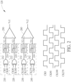
- FIG. 2 is a diagram illustrating the quadrature phase detector 120 according to one embodiment of the present invention.
- the quadrature phase detector 120 comprises a first detection circuit 210, a second detection circuit 220, a third detection circuit 230, a fourth detection circuit 240, a first comparator 250 and a second comparator 260, wherein the first detection circuit 210 comprises an XOR gate 212 and a low-pass filter 214, the second detection circuit 220 comprises an XOR gate 222 and a low-pass filter 224, the third detection circuit 230 comprises an XOR gate 232 and a low-pass filter 234, and the fourth detection circuit 240 comprises an XOR gate 242 and a low-pass filter 244.
- the XOR gate 212 receives the clock signals CK0 and CK90 to generate a first output signal, wherein the first output signal has a high voltage (i.e., a high voltage level of the clock signal CK0 or a supply voltage VDD) only when the clock signal CK0 has a high voltage level and the clock signal CK90 has a low voltage level, and the first output signal has a low voltage (e.g., ground voltage or 0V) when both the clock signal CK0 and the clock signal CK90 have the high voltage levels or the clock signal CK0 has the low voltage level.
- a high voltage i.e., a high voltage level of the clock signal CK0 or a supply voltage VDD
- a first detection result V1 generated by filtering the first output signal is equal to (1/4) *VDD if the phase difference between the clock signals CK0 and CK90 is exactly equal to 90 degrees.
- the XOR gate 222 receives the clock signals CK90 and CK180 to generate a second output signal, wherein the second output signal has a high voltage only when the clock signal CK90 has a high voltage level and the clock signal CK180 has a low voltage level, and the second output signal has a low voltage when both the clock signal CK90 and the clock signal CK180 have the high voltage levels or the clock signal CK90 has the low voltage level.
- a first detection result V2 generated by filtering the second output signal is equal to (1/4) *VDD if the phase difference between the clock signals CK90 and CK180 is exactly equal to 90 degrees.
- the XOR gate 232 receives the clock signals CK180 and CK270 to generate a third output signal, wherein the third output signal has a high voltage only when the clock signal CK180 has a high voltage level and the clock signal CK270 has a low voltage level, and the third output signal has a low voltage when both the clock signal CK180 and the clock signal CK270 have the high voltage levels or the clock signal CK180 has the low voltage level.
- a third detection result V3 generated by filtering the third output signal is equal to (1/4)*VDD if the phase difference between the clock signals CK180 and CK270 is exactly equal to 90 degrees.
- the XOR gate 242 receives the clock signals CK270 and CK0 to generate a fourth output signal, wherein the fourth output signal has a high voltage only when the clock signal CK270 has a high voltage level and the clock signal CK0 has a low voltage level, and the fourth output signal has a low voltage when both the clock signal CK270 and the clock signal CK0 have the high voltage levels or the clock signal CK270 has the low voltage level.
- a fourth detection result V4 generated by filtering the fourth output signal is equal to (1/4)*VDD if the phase difference between the clock signals CK270 and CK0 is exactly equal to 90 degrees.
- the first comparator 250 compares the first detection result V1 and the second detection result V2 to generate the control signal Vc1 to control the resistance of the transistor M1. Specifically, if the first detection result V1 is greater than the second detection result V2, it may indicate that the phase difference between the clock signals CK0 and CK90 is greater than the phase difference between the clock signals CK90 and CK180, then the first comparator 250 can generate the control signal Vc1 to lower the resistance of the transistor M1 to advance the phase of the clock signal CK90.
- the first comparator 250 can generate the control signal Vc1 to increase the resistance of the transistor M1 to delay the phase of the clock signal CK90.
- the second comparator 260 compares the third detection result V3 and the fourth detection result V4 to generate the control signal Vc2 to control the resistance of the transistor M2. Specifically, if the third detection result V3 is greater than the fourth detection result V4, it may indicate that the phase difference between the clock signals CK180 and CK270 is greater than the phase difference between the clock signals CK270 and CK0, then the second comparator 260 can generate the control signal Vc2 to lower the resistance of the transistor M2 to advance the phase of the clock signal CK270.
- the second comparator 260 can generate the control signal Vc2 to increase the resistance of the transistor M2 to delay the phase of the clock signal CK270.
- the phases of the clock signals CK90 and CK270 can be controlled so that the phases of the clock signals CK90 and CK270 approach 90 degrees and 270 degrees, respectively.
- the detailed circuits within the quadrature phase detector 120 are for illustrative, not a limitation of the present invention.
- the XOR gate 212/222/232/242 can be replaced by other logical circuit(s), and/or the first detection circuit 210, the second detection circuit 220 and the first comparator 250 can be combined to detect the phases of the clock signals CK0, CK90 and CK180 to generate the control circuit Vc1, and/or the third detection circuit 230, the fourth detection circuit 240 and the second comparator 260 can be combined to detect the phases of the clock signals CK180, CK270 and CK0 to generate the control signal Vc2.
- the quadrature phase detector 120 can generate the control signal V1 based on the clock signals CK0, CK90 and CK180, and generate the control signal Vc2 based on the clock signals CK180, CK270 and CK0, the quadrature phase detector 120 can have different circuit designs inside.
- the first path and the fourth path do not have any adjustable delay circuit, and only the second path and the third path have the adjustable delay circuits, therefore, the noise, power consumption and the mismatch of the poly phase filter can be greatly improved.
- the quadrature phase detector to detect the phases of the clock signals, the adjustable delay circuits of the second path and the third path can be controlled well so that the clock signals have the appropriate phases.
Landscapes
- Physics & Mathematics (AREA)
- Nonlinear Science (AREA)
- Engineering & Computer Science (AREA)
- Power Engineering (AREA)
- Manipulation Of Pulses (AREA)
- Networks Using Active Elements (AREA)
Abstract
Description
- This application claims the benefit of
U.S. Provisional Application No. 63/255, 029, filed on October 13th, 2021 - In a conventional poly phase filter with multiple paths, each path has an adjustable delay circuit for controlling the phase of the corresponding output clock signal to make all the output clock signals of the poly phase filter have the appropriate phases. However, the mismatch between each path will greatly introduce large phase error.
- It is therefore an objective of the present invention to provide a poly phase filter with less adjustable delay circuits, to solve the above-mentioned problems.
- According to one embodiment of the present invention, a filtering circuit comprising a poly phase filter and a quadrature phase detector is disclosed. The poly phase filter comprises a first path, a second path, a third path and a fourth path. The first path is configured to receive a first input signal to generate a first clock signal. The second path comprising a first adjustable delay circuit is configured to receive the first input signal to generate a second clock signal, wherein the first adjustable delay circuit is coupled to the first input signal and a second input signal, and the first input signal and the second input signal is a differential signal. The third path comprising a second adjustable delay circuit is configured to receive the second input signal to generate a third clock signal, wherein the second adjustable delay circuit is coupled to the first input signal and the second input signal. The fourth path is configured to receive the second input signal to generate a fourth clock signal. The quadrature phase detector is configured to detect phases of the first clock signal, the second clock signal, the third clock signal and the fourth clock signal to generate control signals to control the first adjustable delay circuit and the second adjustable delay circuit.
- According to one embodiment of the present invention, a poly phase filter comprising a first path, a second path, a third path and a fourth path is disclosed. The first path is configured to receive a first input signal to generate a first clock signal. The second path comprising a first adjustable delay circuit is configured to receive the first input signal to generate a second clock signal, wherein the first adjustable delay circuit is coupled to the first input signal and a second input signal, and the first input signal and the second input signal is a differential signal. The third path comprising a second adjustable delay circuit is configured to receive the second input signal to generate a third clock signal, wherein the second adjustable delay circuit is coupled to the first input signal and the second input signal. The fourth path is configured to receive the second input signal to generate a fourth clock signal.
- These and other objectives of the present invention will no doubt become obvious to those of ordinary skill in the art after reading the following detailed description of the preferred embodiment that is illustrated in the various figures and drawings.
-
-
FIG. 1 is a diagram illustrating a filtering circuit comprising a poly phase filter and a quadrature phase detector according to one embodiment of the present invention. -
FIG. 2 is a diagram illustrating the quadrature phase detector according to one embodiment of the present invention. - Certain terms are used throughout the following description and claims to refer to particular system components. As one skilled in the art will appreciate, manufacturers may refer to a component by different names. This document does not intend to distinguish between components that differ in name but not function. In the following discussion and in the claims, the terms "including" and "comprising" are used in an open-ended fashion, and thus should be interpreted to mean "including, but not limited to ...". The terms "couple" and "couples" are intended to mean either an indirect or a direct electrical connection. Thus, if a first device couples to a second device, that connection may be through a direct electrical connection, or through an indirect electrical connection via other devices and connections.
-
FIG. 1 is a diagram illustrating afiltering circuit 100 according to one embodiment of the present invention. As shown inFIG. 1 , thefiltering circuit 100 comprises apoly phase filter 110 and aquadrature phase detector 120, wherein thepoly phase filter 110 is configured to receive a differential input signal (clock signal) VIP and VIN to generate four clock signals CK0, CK90, CK180 and CK270 with ideal phases of 0 degree, 90 degrees, 180 degrees and 270 degrees, respectively, and thequadrature phase detector 120 is configured to detect phases of the clock signals CK0, CK90, CK180 and CK270 to generate control signals Vc1 and Vc2 to control the internal delay of thepoly phase filter 110. - The
poly phase filter 110 comprises four paths for generating the clock signals CK0, CK90, CK270 and CK180 with the same frequency, respectively. The first path comprises abuffer 112, and thebuffer 112 receives the input signal VIP to generate the clock signal CK0, that is the input signal VIP serves as the clock signal CK0. The second path comprises an adjustable delay circuit (in this embodiment, a transistor M1 serves as the adjustable delay circuit), a capacitor C1 and abuffer 114, wherein a gate electrode of the transistor M1 is coupled to the control signal Vc1, a first electrode of the transistor M1 is coupled to the input signal VIP, a second electrode of the transistor M1 is used to generate the clock signal CK90 via thebuffer 114, and the capacitor C1 is coupled between the second electrode of the transistor M1 and the input signal VIN. The third path comprises an adjustable delay circuit (in this embodiment, a transistor M2 serves as the adjustable delay circuit), a capacitor C2 and abuffer 116, wherein a gate electrode of the transistor M2 is coupled to the control signal Vc2, a first electrode of the transistor M2 is coupled to the input signal VIN, a second electrode of the transistor M2 is used to generate the clock signal CK270 via thebuffer 116, and the capacitor C2 is coupled between the second electrode of the transistor M1 and the input signal VIP. The fourth path comprises abuffer 118, and thebuffer 118 receives the input signal VIN to generate the clock signal CK180, that is the input signal VIN serves as the clock signal CK180. - In the
poly phase filter 110 shown inFIG. 1 , the input signal VIP serves as the clock signal CK0 directly, the transistor M1 and the capacitor C1 perform phase interpolation on the input signals VIP and VIN to generate the clock signal CK90, the transistor M2 and the capacitor C2 perform phase interpolation on the input signals VIP and VIN to generate the clock signal CK270, and the input signal VIN serves as the clock signal CK180 directly. Therefore, because the first path and the fourth path do not have any adjustable delay circuit, and only the second path and the third path have the adjustable delay circuits M1 and M2, the noise, power consumption and the mismatch of thepoly phase filter 110 can be greatly improved. -
FIG. 2 is a diagram illustrating thequadrature phase detector 120 according to one embodiment of the present invention. As shown inFIG. 2 , thequadrature phase detector 120 comprises afirst detection circuit 210, asecond detection circuit 220, athird detection circuit 230, a fourth detection circuit 240, afirst comparator 250 and asecond comparator 260, wherein thefirst detection circuit 210 comprises anXOR gate 212 and a low-pass filter 214, thesecond detection circuit 220 comprises anXOR gate 222 and a low-pass filter 224, thethird detection circuit 230 comprises anXOR gate 232 and a low-pass filter 234, and the fourth detection circuit 240 comprises anXOR gate 242 and a low-pass filter 244. - In the operation of the
first detection circuit 210 of thequadrature phase detector 120, theXOR gate 212 receives the clock signals CK0 and CK90 to generate a first output signal, wherein the first output signal has a high voltage (i.e., a high voltage level of the clock signal CK0 or a supply voltage VDD) only when the clock signal CK0 has a high voltage level and the clock signal CK90 has a low voltage level, and the first output signal has a low voltage (e.g., ground voltage or 0V) when both the clock signal CK0 and the clock signal CK90 have the high voltage levels or the clock signal CK0 has the low voltage level. Since the first output signal has the high voltage only during quarter-cycle of the clock signal CK0/CK90, a first detection result V1 generated by filtering the first output signal is equal to (1/4) *VDD if the phase difference between the clock signals CK0 and CK90 is exactly equal to 90 degrees. - Regarding the operation of the
second detection circuit 220, theXOR gate 222 receives the clock signals CK90 and CK180 to generate a second output signal, wherein the second output signal has a high voltage only when the clock signal CK90 has a high voltage level and the clock signal CK180 has a low voltage level, and the second output signal has a low voltage when both the clock signal CK90 and the clock signal CK180 have the high voltage levels or the clock signal CK90 has the low voltage level. Since the second output signal has the high voltage only during quarter-cycle of the clock signal CK90/CK180, a first detection result V2 generated by filtering the second output signal is equal to (1/4) *VDD if the phase difference between the clock signals CK90 and CK180 is exactly equal to 90 degrees. - Regarding the operation of the
third detection circuit 230, theXOR gate 232 receives the clock signals CK180 and CK270 to generate a third output signal, wherein the third output signal has a high voltage only when the clock signal CK180 has a high voltage level and the clock signal CK270 has a low voltage level, and the third output signal has a low voltage when both the clock signal CK180 and the clock signal CK270 have the high voltage levels or the clock signal CK180 has the low voltage level. Since the third output signal has the high voltage only during quarter-cycle of the clock signal CK180/CK270, a third detection result V3 generated by filtering the third output signal is equal to (1/4)*VDD if the phase difference between the clock signals CK180 and CK270 is exactly equal to 90 degrees. - Regarding the operation of the fourth detection circuit 240, the
XOR gate 242 receives the clock signals CK270 and CK0 to generate a fourth output signal, wherein the fourth output signal has a high voltage only when the clock signal CK270 has a high voltage level and the clock signal CK0 has a low voltage level, and the fourth output signal has a low voltage when both the clock signal CK270 and the clock signal CK0 have the high voltage levels or the clock signal CK270 has the low voltage level. Since the fourth output signal has the high voltage only during quarter-cycle of the clock signal CK270/CK0, a fourth detection result V4 generated by filtering the fourth output signal is equal to (1/4)*VDD if the phase difference between the clock signals CK270 and CK0 is exactly equal to 90 degrees. - Then, the
first comparator 250 compares the first detection result V1 and the second detection result V2 to generate the control signal Vc1 to control the resistance of the transistor M1. Specifically, if the first detection result V1 is greater than the second detection result V2, it may indicate that the phase difference between the clock signals CK0 and CK90 is greater than the phase difference between the clock signals CK90 and CK180, then thefirst comparator 250 can generate the control signal Vc1 to lower the resistance of the transistor M1 to advance the phase of the clock signal CK90. If the first detection result V1 is less than the second detection result V2, it may indicate that the phase difference between the clock signals CK0 and CK90 is less than the phase difference between the clock signals CK90 and CK180, then thefirst comparator 250 can generate the control signal Vc1 to increase the resistance of the transistor M1 to delay the phase of the clock signal CK90. - Similarly, the
second comparator 260 compares the third detection result V3 and the fourth detection result V4 to generate the control signal Vc2 to control the resistance of the transistor M2. Specifically, if the third detection result V3 is greater than the fourth detection result V4, it may indicate that the phase difference between the clock signals CK180 and CK270 is greater than the phase difference between the clock signals CK270 and CK0, then thesecond comparator 260 can generate the control signal Vc2 to lower the resistance of the transistor M2 to advance the phase of the clock signal CK270. If the third detection result V3 is less than the fourth detection result V4, it may indicate that the phase difference between the clock signals CK180 and CK270 is less than the phase difference between the clock signals CK270 and CK0, then thesecond comparator 260 can generate the control signal Vc2 to increase the resistance of the transistor M2 to delay the phase of the clock signal CK270. - By using the
quadrature phase detector 120 shown inFIG. 2 , the phases of the clock signals CK90 and CK270 can be controlled so that the phases of the clock signals CK90 and CK270 approach 90 degrees and 270 degrees, respectively. - It is noted that the detailed circuits within the
quadrature phase detector 120 are for illustrative, not a limitation of the present invention. For example, theXOR gate 212/222/232/242 can be replaced by other logical circuit(s), and/or thefirst detection circuit 210, thesecond detection circuit 220 and thefirst comparator 250 can be combined to detect the phases of the clock signals CK0, CK90 and CK180 to generate the control circuit Vc1, and/or thethird detection circuit 230, the fourth detection circuit 240 and thesecond comparator 260 can be combined to detect the phases of the clock signals CK180, CK270 and CK0 to generate the control signal Vc2. In other words, as long as thequadrature phase detector 120 can generate the control signal V1 based on the clock signals CK0, CK90 and CK180, and generate the control signal Vc2 based on the clock signals CK180, CK270 and CK0, thequadrature phase detector 120 can have different circuit designs inside. - Briefly summarized, in the poly phase filter of the present invention, the first path and the fourth path do not have any adjustable delay circuit, and only the second path and the third path have the adjustable delay circuits, therefore, the noise, power consumption and the mismatch of the poly phase filter can be greatly improved. In addition, by using the quadrature phase detector to detect the phases of the clock signals, the adjustable delay circuits of the second path and the third path can be controlled well so that the clock signals have the appropriate phases.
- Those skilled in the art will readily observe that numerous modifications and alterations of the device and method may be made while retaining the teachings of the invention. Accordingly, the above disclosure should be construed as limited only by the metes and bounds of the appended claims.
Claims (13)
- A filtering circuit (100), comprising:a poly phase filter (110), comprising:a first path, configured to receive a first input signal to generate a first clock signal;a second path comprising a first adjustable delay circuit, configured to receive the first input signal to generate a second clock signal, wherein the first adjustable delay circuit is coupled to the first input signal and a second input signal, and the first input signal and the second input signal is a differential signal;a third path comprising a second adjustable delay circuit, configured to receive the second input signal to generate a third clock signal, wherein the second adjustable delay circuit is coupled to the first input signal and the second input signal; anda fourth path, configured to receive the second input signal to generate a fourth clock signal; anda quadrature phase detector (120), configured to detect phases of the first clock signal, the second clock signal, the third clock signal and the fourth clock signal to generate control signals to control the first adjustable delay circuit and the second adjustable delay circuit.
- The filtering circuit (100) of claim 1, wherein the first path does not have any adjustable delay circuit, and the fourth path does not have any adjustable circuit.
- The filtering circuit (100) of claim 1, wherein the first adjustable delay circuit has a first electrode and a second electrode, the first adjustable delay circuit receives the first input signal at the first electrode, and outputs the second clock signal at the second electrode; and the second electrode of the first adjustable delay circuit is coupled to the second input signal via a first capacitor.
- The filtering circuit (100) of claim 3, wherein the second adjustable delay circuit has a first electrode and a second electrode, the second adjustable delay circuit receives the second input signal at the first electrode, and outputs the third clock signal at the second electrode; and the second electrode of the second adjustable delay circuit is coupled to the first input signal via a second capacitor.
- The filtering circuit (100) of claim 1, wherein the quadrature phase detector (120) detects the phases of the first clock signal, the second clock signal and the fourth clock signal to generate a first control signal of the control signals to control the first adjustable delay circuit.
- The filtering circuit (100) of claim 5, wherein the quadrature phase detector (120) detects the phases of the first clock signal, the third clock signal and the fourth clock signal to generate a second control signal of the control signals to control the second adjustable delay circuit.
- The filtering circuit (100) of claim 6, wherein the first clock signal, the second clock signal, the third clock signal and the fourth clock signal correspond to phases of 0 degree, 90 degrees, 180 degrees and 270 degrees, respectively.
- The filtering circuit (100) of claim 6, wherein the quadrature phase detector (120) comprises:a first detection circuit (210), configured to detect a phase difference between the first clock signal and the second clock signal to generate a first detection result;a second detection circuit (220), configured to detect a phase difference between the second clock signal and the third clock signal to generate a second detection result;a third detection circuit (230), configured to detect a phase difference between the third clock signal and the fourth clock signal to generate a third detection result;a fourth detection result, configured to detect a phase difference between the fourth clock signal and the first clock signal to generate a fourth detection result;a first comparator (250), configured to compare the first detection result and the second detection result to generate the first control signal; anda second comparator (260), configured to compare the third detection result and the fourth detection result to generate the second control signal.
- A poly phase filter (110), comprising:a first path, configured to receive a first input signal to generate a first clock signal;a second path comprising a first adjustable delay circuit, configured to receive the first input signal to generate a second clock signal, wherein the first adjustable delay circuit is coupled to the first input signal and a second input signal, and the first input signal and the second input signal is a differential signal;a third path comprising a second adjustable delay circuit, configured to receive the second input signal to generate a third clock signal, wherein the second adjustable delay circuit is coupled to the first input signal and the second input signal; anda fourth path, configured to receive the second input signal to generate a fourth clock signal.
- The poly phase filter (110) of claim 9, wherein the first path does not have any adjustable delay circuit, and the fourth path does not have any adjustable circuit.
- The poly phase filter (110) of claim 9, wherein the first adjustable delay circuit has a first electrode and a second electrode, the first adjustable delay circuit receives the first input signal at the first electrode, and outputs the second clock signal at the second electrode; and the second electrode of the first adjustable delay circuit is coupled to the second input signal via a first capacitor.
- The poly phase filter (110) of claim 9, wherein the second adjustable delay circuit has a first electrode and a second electrode, the second adjustable delay circuit receives the second input signal at the first electrode, and outputs the third clock signal at the second electrode; and the second electrode of the second adjustable delay circuit is coupled to the first input signal via a second capacitor.
- The poly phase filter (110) of claim 9, wherein the first clock signal, the second clock signal, the third clock signal and the fourth clock signal correspond to phases of 0 degree, 90 degrees, 180 degrees and 270 degrees, respectively.
Applications Claiming Priority (2)
| Application Number | Priority Date | Filing Date | Title |
|---|---|---|---|
| US202163255029P | 2021-10-13 | 2021-10-13 | |
| US17/864,416 US11811413B2 (en) | 2021-10-13 | 2022-07-14 | Poly phase filter with phase error enhance technique |
Publications (1)
| Publication Number | Publication Date |
|---|---|
| EP4167488A1 true EP4167488A1 (en) | 2023-04-19 |
Family
ID=82939888
Family Applications (1)
| Application Number | Title | Priority Date | Filing Date |
|---|---|---|---|
| EP22190376.8A Pending EP4167488A1 (en) | 2021-10-13 | 2022-08-15 | Poly phase filter with phase error enhance technique |
Country Status (4)
| Country | Link |
|---|---|
| US (1) | US11811413B2 (en) |
| EP (1) | EP4167488A1 (en) |
| CN (1) | CN115967370A (en) |
| TW (1) | TWI833335B (en) |
Cited By (1)
| Publication number | Priority date | Publication date | Assignee | Title |
|---|---|---|---|---|
| US20220200781A1 (en) * | 2020-12-18 | 2022-06-23 | Intel Corporation | Wide-range inductor-based delay-cell and area efficient termination switch control |
Families Citing this family (1)
| Publication number | Priority date | Publication date | Assignee | Title |
|---|---|---|---|---|
| CN118631244B (en) * | 2024-06-11 | 2025-08-12 | 上海钫铖微电子有限公司 | Detection circuit and control method for phase alignment between multiple groups of multi-phase orthogonal clocks |
Citations (3)
| Publication number | Priority date | Publication date | Assignee | Title |
|---|---|---|---|---|
| WO1992011704A1 (en) * | 1990-12-21 | 1992-07-09 | Motorola, Inc. | Apparatus and method for generating quadrature signals |
| US9490826B1 (en) * | 2015-08-19 | 2016-11-08 | Qualcomm Incorporated | Methods and apparatus for synchronizing frequency dividers using a pulse swallowing technique |
| EP3419166A1 (en) * | 2016-02-17 | 2018-12-26 | Mitsubishi Electric Corporation | Poly-phase filter and filter circuit |
Family Cites Families (15)
| Publication number | Priority date | Publication date | Assignee | Title |
|---|---|---|---|---|
| CN100449952C (en) * | 2001-01-12 | 2009-01-07 | 硅谷实验室公司 | Separation of radio frequency devices and related methods |
| KR100395213B1 (en) * | 2001-03-22 | 2003-08-21 | 주식회사 버카나와이어리스코리아 | Quadrature Signal Generator and Phase Error Correction Method |
| US7386286B2 (en) * | 2001-06-01 | 2008-06-10 | Broadband Innovations, Inc. | High frequency low noise phase-frequency detector and phase noise reduction method and apparatus |
| US7356106B2 (en) | 2004-09-07 | 2008-04-08 | Agency For Science, Technology And Research | Clock and data recovery circuit |
| KR100618347B1 (en) * | 2005-02-01 | 2006-08-31 | 삼성전자주식회사 | Quadrature signal generator with phase adjustment for all four quadrature signals |
| US8111734B2 (en) * | 2008-01-14 | 2012-02-07 | The Boeing Company | Device and method for fast transition from preamble synchronization to data demodulation in direct sequence spread spectrum (DSSS) communications |
| US7872924B2 (en) * | 2008-10-28 | 2011-01-18 | Micron Technology, Inc. | Multi-phase duty-cycle corrected clock signal generator and memory having same |
| WO2011004423A1 (en) * | 2009-07-06 | 2011-01-13 | 富士通株式会社 | Polyphase filter and single side band mixer comprising the polyphase filter |
| WO2012002023A1 (en) * | 2010-06-29 | 2012-01-05 | 日本電気株式会社 | Frequency converter and receiver using same |
| US9106202B2 (en) * | 2013-04-17 | 2015-08-11 | Linear Technology Corporation | Poly-phase filter with phase tuning |
| US9444435B1 (en) * | 2015-10-20 | 2016-09-13 | Stmicroelectronics S.R.L. | Injection locked ring oscillator circuit with an analog quadrature calibration loop |
| US11550354B2 (en) * | 2020-02-18 | 2023-01-10 | Taiwan Semiconductor Manufacturing Company Limited | Systems and methods for multi-phase clock generation |
| US10963002B1 (en) * | 2020-06-02 | 2021-03-30 | Qualcomm Incorporated | Clock generation architecture using a poly-phase filter with self-correction capability |
| US11271710B1 (en) * | 2020-11-30 | 2022-03-08 | Renesas Electronics Corporation | Wideband quadrature phase generation using tunable polyphase filter |
| US11258436B1 (en) * | 2021-04-09 | 2022-02-22 | Realtek Semiconductor Corp. | Self-calibrating quadrature clock generator and method thereof |
-
2022
- 2022-07-14 US US17/864,416 patent/US11811413B2/en active Active
- 2022-07-25 CN CN202210876659.8A patent/CN115967370A/en active Pending
- 2022-08-15 EP EP22190376.8A patent/EP4167488A1/en active Pending
- 2022-08-22 TW TW111131447A patent/TWI833335B/en active
Patent Citations (3)
| Publication number | Priority date | Publication date | Assignee | Title |
|---|---|---|---|---|
| WO1992011704A1 (en) * | 1990-12-21 | 1992-07-09 | Motorola, Inc. | Apparatus and method for generating quadrature signals |
| US9490826B1 (en) * | 2015-08-19 | 2016-11-08 | Qualcomm Incorporated | Methods and apparatus for synchronizing frequency dividers using a pulse swallowing technique |
| EP3419166A1 (en) * | 2016-02-17 | 2018-12-26 | Mitsubishi Electric Corporation | Poly-phase filter and filter circuit |
Non-Patent Citations (1)
| Title |
|---|
| PIRI FARSHAD ET AL: "A PVT-Tolerant >40-dB IRR, 44% Fractional-Bandwidth Ultra-Wideband mm-Wave Quadrature LO Generator for 5G Networks in 55-nm CMOS", IEEE JOURNAL OF SOLID-STATE CIRCUITS, IEEE, USA, vol. 53, no. 12, 1 December 2018 (2018-12-01), pages 3576 - 3586, XP011701017, ISSN: 0018-9200, [retrieved on 20181218], DOI: 10.1109/JSSC.2018.2878819 * |
Cited By (2)
| Publication number | Priority date | Publication date | Assignee | Title |
|---|---|---|---|---|
| US20220200781A1 (en) * | 2020-12-18 | 2022-06-23 | Intel Corporation | Wide-range inductor-based delay-cell and area efficient termination switch control |
| US12184751B2 (en) * | 2020-12-18 | 2024-12-31 | Intel Corporation | Wide-range inductor-based delay-cell and area efficient termination switch control |
Also Published As
| Publication number | Publication date |
|---|---|
| TWI833335B (en) | 2024-02-21 |
| US11811413B2 (en) | 2023-11-07 |
| TW202316795A (en) | 2023-04-16 |
| CN115967370A (en) | 2023-04-14 |
| US20230114343A1 (en) | 2023-04-13 |
Similar Documents
| Publication | Publication Date | Title |
|---|---|---|
| US10873444B2 (en) | Frequency/phase lock detector for clock and data recovery circuits | |
| EP3520219B1 (en) | High speed driver with adaptive termination impedance | |
| US10892742B2 (en) | Duty-cycle calibration based on differential clock sensing | |
| US11811413B2 (en) | Poly phase filter with phase error enhance technique | |
| US11121851B2 (en) | Differential sensing circuit for clock skew calibration relative to reference clock | |
| US10097183B2 (en) | Level shifter and method of calibration | |
| CN113364452B (en) | Clock data recovery device and clock data recovery method | |
| JP4263023B2 (en) | Two-wire data communication method, system, control device and data storage device | |
| CN108809279B (en) | Duty ratio calibration circuit and radio frequency terminal | |
| US6794919B1 (en) | Devices and methods for automatically producing a clock signal that follows the master clock signal | |
| US7772853B2 (en) | Semiconductor device | |
| US20050156678A1 (en) | Voltage control oscillator | |
| CN117044108B (en) | Delay cell for quadrature clock generation with equal rising/falling edges and insensitive to PVT variations | |
| TWI761162B (en) | Signal processing circuit | |
| US20190199337A1 (en) | Comparator | |
| US12212325B2 (en) | Low power quadrature phase detector | |
| US20070146017A1 (en) | Semiconductor device | |
| US9595898B1 (en) | Device for controlling motor driving | |
| US11942950B2 (en) | Input clock buffer and clock signal buffereing method | |
| JP4430117B2 (en) | Data storage device | |
| US20260012182A1 (en) | Voltage level shifter | |
| CN121283403A (en) | Voltage level shifter | |
| CN115580297A (en) | Phase-locked loop circuit with extremely low jitter and phase-locked loop module | |
| TW202211606A (en) | Charge pump device | |
| TW201519579A (en) | Input signal voltage detection module and method, and related data transmission system |
Legal Events
| Date | Code | Title | Description |
|---|---|---|---|
| PUAI | Public reference made under article 153(3) epc to a published international application that has entered the european phase |
Free format text: ORIGINAL CODE: 0009012 |
|
| STAA | Information on the status of an ep patent application or granted ep patent |
Free format text: STATUS: THE APPLICATION HAS BEEN PUBLISHED |
|
| AK | Designated contracting states |
Kind code of ref document: A1 Designated state(s): AL AT BE BG CH CY CZ DE DK EE ES FI FR GB GR HR HU IE IS IT LI LT LU LV MC MK MT NL NO PL PT RO RS SE SI SK SM TR |
|
| P01 | Opt-out of the competence of the unified patent court (upc) registered |
Effective date: 20230607 |
|
| STAA | Information on the status of an ep patent application or granted ep patent |
Free format text: STATUS: REQUEST FOR EXAMINATION WAS MADE |
|
| 17P | Request for examination filed |
Effective date: 20231017 |
|
| RBV | Designated contracting states (corrected) |
Designated state(s): AL AT BE BG CH CY CZ DE DK EE ES FI FR GB GR HR HU IE IS IT LI LT LU LV MC MK MT NL NO PL PT RO RS SE SI SK SM TR |
|
| STAA | Information on the status of an ep patent application or granted ep patent |
Free format text: STATUS: EXAMINATION IS IN PROGRESS |