EP4167479A1 - Group delay determination in a communication circuit - Google Patents
Group delay determination in a communication circuit Download PDFInfo
- Publication number
- EP4167479A1 EP4167479A1 EP22201414.4A EP22201414A EP4167479A1 EP 4167479 A1 EP4167479 A1 EP 4167479A1 EP 22201414 A EP22201414 A EP 22201414A EP 4167479 A1 EP4167479 A1 EP 4167479A1
- Authority
- EP
- European Patent Office
- Prior art keywords
- current
- voltage
- signal
- modulated
- rectangular
- Prior art date
- Legal status (The legal status is an assumption and is not a legal conclusion. Google has not performed a legal analysis and makes no representation as to the accuracy of the status listed.)
- Pending
Links
Images





Classifications
-
- H—ELECTRICITY
- H03—ELECTRONIC CIRCUITRY
- H03F—AMPLIFIERS
- H03F3/00—Amplifiers with only discharge tubes or only semiconductor devices as amplifying elements
- H03F3/189—High-frequency amplifiers, e.g. radio frequency amplifiers
- H03F3/19—High-frequency amplifiers, e.g. radio frequency amplifiers with semiconductor devices only
-
- H—ELECTRICITY
- H03—ELECTRONIC CIRCUITRY
- H03K—PULSE TECHNIQUE
- H03K5/00—Manipulating of pulses not covered by one of the other main groups of this subclass
- H03K5/01—Shaping pulses
- H03K5/04—Shaping pulses by increasing duration; by decreasing duration
- H03K5/06—Shaping pulses by increasing duration; by decreasing duration by the use of delay lines or other analogue delay elements
-
- H—ELECTRICITY
- H03—ELECTRONIC CIRCUITRY
- H03F—AMPLIFIERS
- H03F1/00—Details of amplifiers with only discharge tubes, only semiconductor devices or only unspecified devices as amplifying elements
- H03F1/02—Modifications of amplifiers to raise the efficiency, e.g. gliding Class A stages, use of an auxiliary oscillation
- H03F1/0205—Modifications of amplifiers to raise the efficiency, e.g. gliding Class A stages, use of an auxiliary oscillation in transistor amplifiers
- H03F1/0211—Modifications of amplifiers to raise the efficiency, e.g. gliding Class A stages, use of an auxiliary oscillation in transistor amplifiers with control of the supply voltage or current
- H03F1/0216—Continuous control
- H03F1/0222—Continuous control by using a signal derived from the input signal
- H03F1/0227—Continuous control by using a signal derived from the input signal using supply converters
-
- H—ELECTRICITY
- H03—ELECTRONIC CIRCUITRY
- H03F—AMPLIFIERS
- H03F3/00—Amplifiers with only discharge tubes or only semiconductor devices as amplifying elements
- H03F3/20—Power amplifiers, e.g. Class B amplifiers, Class C amplifiers
- H03F3/24—Power amplifiers, e.g. Class B amplifiers, Class C amplifiers of transmitter output stages
- H03F3/245—Power amplifiers, e.g. Class B amplifiers, Class C amplifiers of transmitter output stages with semiconductor devices only
-
- H—ELECTRICITY
- H03—ELECTRONIC CIRCUITRY
- H03K—PULSE TECHNIQUE
- H03K5/00—Manipulating of pulses not covered by one of the other main groups of this subclass
- H03K5/22—Circuits having more than one input and one output for comparing pulses or pulse trains with each other according to input signal characteristics, e.g. slope, integral
- H03K5/24—Circuits having more than one input and one output for comparing pulses or pulse trains with each other according to input signal characteristics, e.g. slope, integral the characteristic being amplitude
-
- H—ELECTRICITY
- H04—ELECTRIC COMMUNICATION TECHNIQUE
- H04B—TRANSMISSION
- H04B1/00—Details of transmission systems, not covered by a single one of groups H04B3/00 - H04B13/00; Details of transmission systems not characterised by the medium used for transmission
- H04B1/38—Transceivers, i.e. devices in which transmitter and receiver form a structural unit and in which at least one part is used for functions of transmitting and receiving
- H04B1/40—Circuits
-
- H—ELECTRICITY
- H03—ELECTRONIC CIRCUITRY
- H03K—PULSE TECHNIQUE
- H03K5/00—Manipulating of pulses not covered by one of the other main groups of this subclass
- H03K2005/00013—Delay, i.e. output pulse is delayed after input pulse and pulse length of output pulse is dependent on pulse length of input pulse
Definitions
- the technology of the disclosure relates generally to determining a group delay in a communication circuit, such as a wireless transmission circuit.
- Mobile communication devices have become increasingly common in current society for providing wireless communication services.
- the prevalence of these mobile communication devices is driven in part by the many functions that are now enabled on such devices.
- Increased processing capabilities in such devices means that mobile communication devices have evolved from being pure communication tools into sophisticated mobile multimedia centers that enable enhanced user experiences.
- a fifth-generation new radio (5G-NR) wireless communication system is widely regarded as a technological advancement that can achieve significantly higher data throughput, improved coverage range, enhanced signaling efficiency, and reduced latency compared to the existing third generation (3G) and fourth generation (4G) communication systems.
- a 5G-NR mobile communication device usually transmits and receives a radio frequency (RF) signal(s) in a millimeter wave (mmWave) RF spectrum that is typically above 6 GHz.
- RF signal(s) transmitted in the mmWave RF spectrum may be more susceptible to propagation attenuation and interference that can result in substantial reduction in data throughput.
- the 5G-NR mobile communication device employs a power amplifier(s) to amplify the RF signal(s) before transmitting in the mmWave RF spectrum.
- Envelope tracking (ET) and average power tracking (APT) are power management techniques designed to improve operating efficiency of the power amplifier(s).
- the power amplifier(s) is configured to amplify the RF signal(s) based on a modulated voltage (ET voltage or APT voltage) that closely tracks a time-variant power envelope of the RF signal(s).
- the time-variant voltage is typically generated by a power management integrated circuit (PMIC) in the wireless communication device.
- PMIC power management integrated circuit
- the modulated voltage and the RF signal(s) may have experienced different group delays when arriving at the power amplifier(s).
- a group delay refers generally to a sum of time delay experienced by a signal propagating through one or more active/passive circuits of different processing capabilities and/or operating frequencies.
- the modulated voltage may become misaligned with the time-variant power envelope of the RF signal(s) at the power amplifier(s) to therefore cause a degraded error vector magnitude (EVM) and/or adjacent channel leakage ratio (ACLR) in the RF signal(s).
- EVM error vector magnitude
- ACLR adjacent channel leakage ratio
- the communication circuit includes a power amplifier circuit that amplifies a radio frequency (RF) signal based on a modulated voltage and a power management integrated circuit (PMIC) that generates the modulated voltage.
- the PMIC includes a group delay determination circuit that is configured to determine a relative group delay between the modulated voltage and a modulated current, which is internal to the power amplifier circuit and unknown to the PMIC, solely based on signals (e.g., voltage, current, etc.) that are known to the PMIC.
- the determined relative group delay can be used to time align the modulated voltage with the modulated current at the power amplifier circuit to thereby improve error vector magnitude (EVM) and/or adjacent channel leakage ratio (ACLR) of the RF signal. Further, by determining the relative group delay based on known signals to the PMIC, it is possible to achieve good time alignment between the modulated voltage and the modulated current.
- EVM error vector magnitude
- ACLR adjacent channel leakage ratio
- a group delay determination circuit includes a signal conversion circuit.
- the signal conversion circuit is configured to receive an analog voltage signal related to a modulated voltage and an analog current signal related to a modulated current.
- the signal conversion circuit is also configured to generate a rectangular voltage signal including multiple voltage rising edges and multiple voltage falling edges based on the received analog voltage signal.
- the signal conversion circuit is also configured to generate a rectangular current signal including multiple current rising edges and multiple current falling edges based on the received analog current signal and the received analog voltage signal.
- the group delay determination circuit also includes a control circuit.
- the control circuit is configured to determine a relative group delay between the modulated voltage and the modulated current based on a relative delay between the rectangular voltage signal and the rectangular current signal.
- a communication circuit in another aspect, includes a power amplifier circuit.
- the power amplifier circuit is configured to amplify an RF signal associated with a time-variant input power based on a modulated voltage and induces a modulated current that tracks the time-variant input power of the RF signal.
- the communication circuit also includes a power amplifier integrated circuit (PMIC).
- the PMIC includes a voltage modulation circuit.
- the voltage modulation circuit is configured to generate the modulated voltage based on a modulated target voltage.
- the PMIC also includes a group delay determination circuit.
- the group delay determination circuit includes a signal conversion circuit.
- the signal conversion circuit is configured to receive an analog voltage signal related to the modulated voltage and an analog current signal related to the modulated current.
- the signal conversion circuit is also configured to generate a rectangular voltage signal including multiple voltage rising edges and multiple voltage falling edges based on the received analog voltage signal.
- the signal conversion circuit is also configured to generate a rectangular current signal including multiple current rising edges and multiple current falling edges based on the received analog current signal and the received analog voltage signal.
- the group delay determination circuit also includes a control circuit. The control circuit is configured to determine a relative group delay between the modulated voltage and the modulated current based on a relative delay between the rectangular voltage signal and the rectangular current signal.
- a method for determining a group delay in a communication circuit includes receiving an analog voltage signal related to a modulated voltage and an analog current signal related to a modulated current.
- the method also includes generating a rectangular voltage signal including multiple voltage rising edges and multiple voltage falling edges based on the received analog voltage signal.
- the method also includes generating a rectangular current signal including multiple current rising edges and multiple current falling edges based on the received analog current signal and the received analog voltage signal.
- the method also includes determining a relative group delay between the modulated voltage and the modulated current based on a relative delay between the rectangular voltage signal and the rectangular current signal.
- the communication circuit includes a power amplifier circuit that amplifies a radio frequency (RF) signal based on a modulated voltage and a power management integrated circuit (PMIC) that generates the modulated voltage.
- the PMIC includes a group delay determination circuit that is configured to determine a relative group delay between the modulated voltage and a modulated current, which is internal to the power amplifier circuit and unknown to the PMIC, solely based on signals (e.g., voltage, current, etc.) that are known to the PMIC.
- the determined relative group delay can be used to time align the modulated voltage with the modulated current at the power amplifier circuit to thereby improve error vector magnitude (EVM) and/or adjacent channel leakage ratio (ACLR) of the RF signal. Further, by determining the relative group delay based on known signals to the PMIC, it is possible to achieve good time alignment between the modulated voltage and the modulated current.
- EVM error vector magnitude
- ACLR adjacent channel leakage ratio
- FIG. 1A is a schematic diagram of an example existing communication circuit 10 wherein a modulated voltage V CC and a modulated current I PA can become time misaligned at a power amplifier circuit 12.
- the existing communication circuit 10 also includes a transceiver circuit 14 and a PMIC 16.
- the transceiver circuit 14 is configured to generate an RF signal 18 having a time-variant input power P IN and provide the RF signal 18 to the power amplifier circuit 12.
- the transceiver circuit 14 also generates a modulated target voltage V TGT that tracks the time-variant input power P IN and provides the modulated target voltage V TGT to the PMIC 16.
- the PMIC 16 is configured to generate a modulated voltage Vcc that tracks the modulated target voltage V TGT and provides the modulated voltage Vcc to the power amplifier circuit 12.
- the modulated target voltage V TGT and the modulated voltage Vcc are time-variant voltages that are so generated (a.k.a. modulated) in accordance with the time-variant input power P IN .
- the transceiver circuit 14 may control (a.k.a. adjust) relative timing between the modulated target voltage V TGT and the RF signal 18 by delaying/advancing one or more of the modulated target voltage V TGT and the RF signal 18.
- the power amplifier circuit 12 is configured to amplify the RF signal 18 from the time-variant input power P IN to a time-variant output power P OUT based on the modulated voltage Vcc.
- the power amplifier circuit 12 often includes a load capacitor C PA to help improve impedance matching between the power amplifier circuit 12 and the PMIC 16.
- the load capacitor C PA can cause a modulated current I PA that closely resembles the time-variant input power P IN of the RF signal 18.
- the modulated current I PA is a time-variant current that varies according to the time-variant input power P IN of the RF signal 18.
- the modulated voltage V CC and the modulated current I PA are typically monotonically related. However, since the modulated voltage V CC is provided by the PMIC 16 and the modulated current I PA is induced internally in the power amplifier circuit 12, the modulated voltage V CC and the modulated current I PA can experience different group delays at the power amplifier circuit 12. As a result, the modulated voltage V CC and the modulated current I PA can become misaligned at the power amplifier circuit 12.
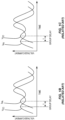
- Figures 1B and 1C illustrate two scenarios where the modulated voltage V CC and the modulated current I PA are misaligned at the power amplifier circuit 12. Specifically, Figure 1B shows that the modulated voltage V CC is ahead of (a.k.a. leading) the modulated current I PA by a relative group delay ⁇ and Figure 1C shows that the modulated voltage Vcc is behind of (a.k.a. trailing) the modulated current I PA by the relative group delay ⁇ .
- the relative group delay ⁇ can cause distortion (e.g., amplitude clipping) in the RF signal 18, which can further lead to a degraded EVM and/or ACLR in the RF signal 18.
- distortion e.g., amplitude clipping
- the relative group delay ⁇ is measured at the power amplifier circuit 12 with a calibration/test equipment of some sort. This proves to be a challenging task given the fact that the existing communication circuit 10 often employs multiple power amplifier circuits made by different vendors. In this regard, it is further desirable to determine the relative group delay ⁇ without complexity associated with the conventional approach.
- FIG 2 is a schematic diagram of an example communication circuit 20, wherein a group delay determination circuit 22 in a PMIC 24 is configured according to embodiments of the present disclosure to determine a relative group delay ⁇ between a modulated voltage Vcc and a modulated current I PA solely based on signals available in the PMIC 24.
- a group delay determination circuit 22 in a PMIC 24 is configured according to embodiments of the present disclosure to determine a relative group delay ⁇ between a modulated voltage Vcc and a modulated current I PA solely based on signals available in the PMIC 24.
- the communication circuit 20 includes a transceiver circuit 26 and the power amplifier circuit 12 in Figure 1A .
- the power amplifier circuit 12 is provided herein to simply illustrate the fact that the PMIC 24 can operate with any power amplifier circuit of any vendor, including but not limited to the power amplifier circuit 12 in the existing communication circuit 10 of Figure 1A .
- the transceiver circuit 26 is configured to generate an RF signal 28 associated with a time-variant input power P IN and the power amplifier circuit 12 is configured to amplify the RF signal 28 from the time-variant input power to a time-variant output power P OUT based on the modulated voltage V CC .
- the power amplifier circuit 12 can induce the modulated current I PA that can be misaligned from the modulated voltage V CC by the relative group delay ⁇ .
- the modulated voltage V CC can either lead or trail behind the modulated current I PA by the relative group delay ⁇ .
- the PMIC 24 Given that the modulated current I PA is induced inside the power amplifier circuit 12, the PMIC 24 would therefore have no direct knowledge about the modulated current I PA . In addition, the PMIC 24 may also have no knowledge about the modulated voltage V CC as received by the power amplifier circuit 12. As such, the group delay determination circuit 22 needs to estimate the relative group delay ⁇ solely based on signals that are available in the PMIC 24.
- the group delay determination circuit 22 is configured to estimate the relative group delay ⁇ based on at least an analog voltage signal 30 that is related to the modulated voltage V CC and an analog current signal 32 that is related to the modulated current I PA .
- the analog voltage signal 30 and the analog current signal 32 are either generated inside the PMIC 24 or provided to the PMIC 24 from outside the PMIC 24.
- the group delay determination circuit 22 is able to determine the relative group delay ⁇ independent of the power amplifier circuit 12.
- the PMIC 24 includes a voltage modulation circuit 34 and a current modulation circuit 36.
- the voltage modulation circuit 34 includes a voltage amplifier 38, an offset capacitor C OFF , and a bypass switch S BYP .
- the voltage amplifier 38 is configured to generate a modulated initial voltage V AMP based on a modulated target voltage V TGT , which is generated by the transceiver circuit 26 to track the time-variant input power P IN of the RF signal 28, and a supply voltage V SUP .
- the offset capacitor C OFF and the bypass switch S BYP are both coupled to an output 40 of the voltage amplifier 38.
- the offset voltage V OFF can be modulated by charging or discharging the offset capacitor C OFF .
- U.S. Patent Application Number 17/946,224 entitled “MULTI-VOLTAGE GENERATION CIRCUIT" (hereinafter "Application224").
- the voltage modulation circuit 34 must maintain the modulated voltage V CC at a desired level.
- the voltage amplifier 38 may source or sink a high-frequency current I AMP (e.g., an alternating current) to allow the load capacitor C PA , which is much smaller than the offset capacitor C OFF , to be quickly charged or discharged to maintain the modulated voltage V CC .
- the high-frequency current I AMP is similar to the modulated current I PA and can thus be utilized to represent the modulated current I PA in the power amplifier circuit 12.
- the voltage amplifier 38 may generate a sensed current I SENSE to proportionally represent the high-frequency current I AMP .
- the sensed current I SENSE is inversely related to the high-frequency current I AMP by a scaling factor k (k > 100). As such, the sensed current I SENSE is smaller than the high-frequency current I AMP .
- the voltage modulation circuit 34 is configured to generate the modulated voltage V CC based on the modulated target voltage V TGT , the modulated voltage V CC will be substantially similar to the modulated voltage V TGT . Accordingly, the modulated target voltage V TGT can be utilized to represent the modulated voltage V CC as received at the power amplifier circuit 12.
- the group delay determination circuit 22 is configured to receive the modulated target voltage V TGT as the analog voltage signal 30 and the sensed current I SENSE as the analog current signal 32. Accordingly, as described below in Figure 3 , the group delay determination circuit 22 is able to determine the relative group delay ⁇ between the modulated voltage V CC and the modulated current I PA by determining the relative group delay ⁇ between the modulated target voltage V TGT and the sensed current I SENSE .
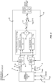
- Figure 3 is a schematic diagram providing an example illustration of the group delay determination circuit 22 in Figure 2 according to an embodiment of the present disclosure. Common elements between Figures 2 and 3 are shown therein with common element numbers and will not be re-described herein.
- the group delay determination circuit 22 includes a signal conversion circuit 42, a first delay circuit 44, a second delay circuit 46, a phase-frequency detector 48, and a control circuit 50.
- the signal conversion circuit 42 receives the analog voltage signal 30 (e.g., the modulated target voltage V TGT ) and the analog current signal 32 (e.g., the sensed current I SENSE ).
- the signal conversion circuit 42 is configured to generate a rectangular current signal 52 (a.k.a. pulse signal), which includes multiple current rising edges 54 and multiple current falling edges 56, based on the analog voltage signal 30.
- the signal conversion circuit 42 is also configured to generate a rectangular voltage signal 58 (a.k.a. pulse signal), which includes multiple voltage rising edges 60 and multiple voltage falling edges 62, based on the received analog current signal 32 and the received analog voltage signal 30.
- Figure 4 is a schematic diagram illustrating the signal conversion circuit 42 in the group delay determination circuit 22 of Figure 3 according to an embodiment of the present disclosure. Common elements between Figures 3 and 4 are shown therein with common element numbers and will not be re-described herein.
- the signal conversion circuit 42 includes a current adjuster 64, a current combiner 66, a first comparator 68, and a second comparator 70.
- the current adjuster 64 is configured to estimate a differential ⁇ I PA between the modulated current I PA and the analog current signal 32, which is equivalent to the sensed current I SENSE , based on the analog voltage signal 30 that is equivalent to the modulated target voltage V TGT .
- the current adjuster 64 can estimate the differential ⁇ I PA based on equation (Eq. 1) below.
- ⁇ I PA C PA / k * dV TGT / dt
- C PA represents a capacitance of the load capacitor C PA in the power amplifier circuit 12 in Figure 2 and k (k > 1) represents the scaling factor between the sensed current I SENSE and the high-frequency current I AMP .
- the differential ⁇ I PA can be either positive or negative.
- the current combiner 66 is configured to combine the analog current signal 32 with the estimated differential ⁇ I PA to generate an estimation I PA-EST that can more accurately represent the modulated current I PA .
- the first comparator 68 is configured to generate the rectangular current signal 52 based on the estimation I PA-EST and a predefined current threshold I PA-TH .
- the second comparator 70 is configured to generate the rectangular voltage signal 58 based on the analog voltage signal 30 and a predefined voltage threshold V TGT-TH .
- the predefined current threshold I PA-TH and the predefined voltage threshold V TGT-TH may be determined to provide a highest possible sensitivity to accurately detect the current rising edges 54, the current falling edges 56, the voltage rising edges 60, and the voltage falling edges 62.
- the voltage amplifier 38 may include such components (e.g., switches) that can cause a parasitic capacitance C EQ that can interact with the modulated initial voltage V AMP to potentially impact the high-frequency current I AMP and, therefore, the sensed current I SENSE .
- switches e.g., switches
- the parasitic capacitance C EQ can interact with the modulated initial voltage V AMP to potentially impact the high-frequency current I AMP and, therefore, the sensed current I SENSE .
- the group delay determination circuit 22 may be further configured to receive a second analog voltage signal 72.
- the second analog voltage signal 72 is the modulated initial voltage V AMP generated by the voltage amplifier 38.
- the signal conversion circuit 42 may further include a second current adjuster 74 to estimate an adjustment term ⁇ I AMP to the analog current signal 32 based on the second analog voltage signal 72.
- the second current adjuster 74 can estimate the adjustment term ⁇ I AMP based on equation (Eq. 2) below.
- ⁇ I AMP C EQ / k * dV AMP / dt
- C EQ represents the parasitic capacitance of the voltage amplifier 38 in the power amplifier circuit 12 in Figure 2 and k (k > 1) represents the scaling factor between the sensed current I SENSE and the high-frequency current I AMP .
- the current combiner 66 is configured to combine the analog current signal 32 with the estimated differential ⁇ I PA and the estimated adjustment term ⁇ I AMP to generate the estimation I PA-EST . Understandably, by further taking into consideration of the parasitic capacitance C EQ , the estimation I PA-EST can represent the modulated current I PA with further improved accuracy.
- control circuit 50 is configured to dynamically delay the rectangular current signal 52 and/or the rectangular voltage signal 58 to thereby cause the rectangular current signal 52 to be in-phase with the rectangular voltage signal 58. Once the rectangular current signal 52 and the rectangular voltage signal 58 become in phase, the control circuit 50 can then determine the relative group delay ⁇ between the rectangular current signal 52 and the rectangular voltage signal 58.
- the control circuit 50 can include a processor 76 (e.g., a digital signal processor) to dynamically control the first delay circuit 44 to delay the rectangular current signal 52 and/or control the second delay circuit 46 to delay the rectangular voltage signal 58. More specifically, the control circuit 50 can control the first delay circuit 44 to delay the rectangular current signal 52 by a first adjustable delay ⁇ 1 to generate a delayed rectangular current signal 78 and/or control the second delay circuit 46 to delay the rectangular voltage signal 58 by a second adjustable delay ⁇ 2 to generate a delayed rectangular voltage signal 80.
- a processor 76 e.g., a digital signal processor
- the delayed rectangular current signal 78 is essentially the same as the rectangular current signal 52, except for a difference in a relative phase. As such, the delayed rectangular current signal 78 will also include the current rising edges 54 and the current falling edges 56.
- the delayed rectangular voltage signal 80 is essentially the same as the rectangular voltage signal 58, except for a difference in a relative phase. As such, the delayed rectangular voltage signal 80 will also include the voltage rising edges 60 and the voltage falling edges 62.
- the phase-frequency detector 48 is configured to determine a phase differential ⁇ ⁇ between the delayed rectangular current signal 78 and the delayed rectangular voltage signal 80. According to an embodiment of the present disclosure, the control circuit 50 can determine that the delayed rectangular current signal 78 and the delayed rectangular voltage signal 80 are in phase when the phase differential ⁇ ⁇ between the delayed rectangular current signal 78 and the delayed rectangular voltage signal 80 is equal to zero ( ⁇ ⁇ 0).
- the phase-frequency detector 48 can include a rising edge phase detector 82, a falling edge phase detector 84, and a combiner 86.
- the rising edge phase detector 82 is configured to detect a rising edge phase offset ⁇ UP between each of the current rising edges 54 and a respective one of the voltage rising edges 60.
- the falling edge phase detector 84 is configured to detect a falling edge phase offset ⁇ DN between each of the current falling edges 56 and a respective one of the voltage falling edges 62.
- the combiner 86 is configured to subtract the falling edge phase offset ⁇ DN from the rising edge phase offset ⁇ UP to generate the phase differential ⁇ ⁇ , as shown in equation (Eq. 3) below.
- ⁇ ⁇ UP ⁇ ⁇ DN
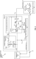
- Figures 5A and 5B are graphic diagrams providing example illustrations as to how the group delay determination circuit 22 of Figure 3 can phase align the delayed rectangular current signal 78 and the delayed rectangular voltage signal 80. Common elements between Figures 3 and 5A-5B are shown therein with common element numbers and will not be re-described herein.
- Figure 5A provides a visual illustration of the delayed rectangular current signal 78 and the delayed rectangular voltage signal 80 that are out of phase. Regardless of whether the delayed rectangular current signal 78 is ahead of the delayed rectangular voltage signal 80 or behind the delayed rectangular voltage signal 80, the rising edge phase offset ⁇ UP is different from the falling edge phase offset ⁇ DN . As a result, according to equation (Eq. 3), the phase differential ⁇ ⁇ will not be equal to zero.
- Figure 5B provides a visual illustration of the delayed rectangular current signal 78 and the delayed rectangular voltage signal 80 that are in phase.
- the rising edge phase offset ⁇ UP is equal to the falling edge phase offset ⁇ DN .
- the phase differential ⁇ ⁇ will be equal to zero.
- the group delay determination circuit 22 may further include a lowpass filter (LPF) 88 and a comparator 90.
- the comparator 90 may operate based on a reference voltage V REF (e.g., 0 V) to help ensure that the phase differential ⁇ ⁇ is equal to zero when the phase differential ⁇ ⁇ is substantially close to zero (e.g., ⁇ 0.01).
- the control circuit 50 may determine the relative group delay ⁇ between the rectangular current signal 52 and the rectangular voltage signal 58 based on equation (Eq. 4) below.
- ⁇ ⁇ 1 ⁇ ⁇ 2 + ⁇ ADJ
- ⁇ 1 represents the first adjustable delay introduced by the first delay circuit 44
- ⁇ 2 represents the second adjustable delay introduced by the second delay circuit 46
- ⁇ ADJ represents a predefined temporal offset that compensates for any estimation error.
- the control circuit 50 may provide the determined relative group delay ⁇ to the transceiver circuit 26 in Figure 2 such that the transceiver circuit 26 can delay or advance the RF signal 28 based on the determined relative group delay ⁇ to thereby ensure that the modulated current I PA is aligned with the modulated voltage V CC at the power amplifier circuit 12.
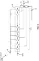
- Figure 6 is a schematic diagram illustrating an example implementation of the first delay circuit 44 and the second delay circuit 46 in the group delay determination circuit 22 of Figure 3 . Common elements between Figures 3 and 6 are shown therein with common element numbers and will not be re-described herein.
- each of the first delay circuit 44 and the second delay circuit 46 can include a respective delay line 92 and a respective multiplexer 94.
- the multiplexer 94 may be controlled by the control circuit 50 in Figure 5 via a control signal 96 to selectively delay the rectangular current signal 52 by the first adjustable delay ⁇ 1 or the rectangular voltage signal 58 by the second adjustable delay ⁇ 2 .
- the delay line 92 may be calibrated by a calibration signal 98.
- Figure 7 is a schematic diagram illustrating an example implementation of the phase-frequency detector 48 in the group delay determination circuit 22 of Figure 3 . Common elements between Figures 3 and 7 are shown therein with common element numbers and will not be re-described herein.
- the current modulation circuit 36 includes a multilevel charge pump (MCP) 100 and a power inductor 102.
- the MCP 100 which can be a buck-boost direct-current (DC) to DC (DC-DC) converter, is configured to generate a low-frequency voltage VDC (e.g., a DC voltage) as a function of a battery voltage V BAT .
- VDC low-frequency voltage
- the MCP 100 may operate in a buck mode to generate the low-frequency voltage V DC at 0 ⁇ V BAT (0 V) or 1 ⁇ V BAT , or in a boost mode to generate the low-frequency voltage V DC at 2 ⁇ V BAT .
- the MCP 100 may toggle between 0 ⁇ V BAT (0 V), 1 ⁇ V BAT , and/or 2 ⁇ V BAT based on a duty cycle 104 to thereby generate the low-frequency voltage V DC at a desired voltage level.
- the current modulation circuit 36 can include a controller 106 (e.g., a microcontroller or a microprocessor) that determines the duty cycle 104 based on the modulated target voltage V TGT .
- the power inductor 102 is configured to induce a low-frequency current I DC based on the low-frequency voltage V DC .
- the low-frequency current I DC is configured to modulate the offset voltage V OFF across the offset capacitor C OFF .
- the communication circuit 20 of Figure 2 can be configured to support group delay determination as described above based on a process.
- Figure 8 is a flowchart of an example process 200 determining the group delay ⁇ in the communication circuit 20 of Figure 2 .
- the group delay determination circuit 22 receives the analog voltage signal 30 that is related to the modulated voltage V CC and the analog current signal 32 that is related to the modulated current I PA (step 202). Next, the group delay determination circuit 22 generates the rectangular voltage signal 58 having the voltage rising edges 60 and the voltage falling edges 62 based on the received analog voltage signal 30 (step 204). The group delay determination circuit 22 also generates the rectangular current signal 52 having the current rising edges 54 and the current falling edges 56 based on the received analog current signal 32 (step 206). Accordingly, the group delay determination circuit 22 determines the relative group delay ⁇ between the modulated voltage V CC and the modulated current I PA based on the relative group delay ⁇ between the rectangular voltage signal 58 and the rectangular current signal 52 (step 208).
- the communication circuit includes a power amplifier circuit that amplifies a radio frequency (RF) signal based on a modulated voltage and a power management integrated circuit (PMIC) that generates the modulated voltage.
- the PMIC includes a group delay determination circuit to determine a relative group delay between the modulated voltage and a modulated current, which is internal to the power amplifier circuit and unknown to the PMIC, solely based on signals known to the PMIC.
- the determined relative group delay can help to time align the modulated voltage with the modulated current at the power amplifier circuit to improve error vector magnitude (EVM) and/or adjacent channel leakage ratio (ACLR).
- EVM error vector magnitude
- ACLR adjacent channel leakage ratio
Landscapes
- Engineering & Computer Science (AREA)
- Physics & Mathematics (AREA)
- Nonlinear Science (AREA)
- Power Engineering (AREA)
- Computer Networks & Wireless Communication (AREA)
- Signal Processing (AREA)
- Amplifiers (AREA)
Abstract
Description
- This application claims the benefit of
U.S. provisional patent application serial number 63/255,662, filed on October 14, 2021 - The technology of the disclosure relates generally to determining a group delay in a communication circuit, such as a wireless transmission circuit.
- Mobile communication devices have become increasingly common in current society for providing wireless communication services. The prevalence of these mobile communication devices is driven in part by the many functions that are now enabled on such devices. Increased processing capabilities in such devices means that mobile communication devices have evolved from being pure communication tools into sophisticated mobile multimedia centers that enable enhanced user experiences.
- A fifth-generation new radio (5G-NR) wireless communication system is widely regarded as a technological advancement that can achieve significantly higher data throughput, improved coverage range, enhanced signaling efficiency, and reduced latency compared to the existing third generation (3G) and fourth generation (4G) communication systems. A 5G-NR mobile communication device usually transmits and receives a radio frequency (RF) signal(s) in a millimeter wave (mmWave) RF spectrum that is typically above 6 GHz. Notably, the RF signal(s) transmitted in the mmWave RF spectrum may be more susceptible to propagation attenuation and interference that can result in substantial reduction in data throughput. To help mitigate propagation attenuation and maintain desirable data throughput, the 5G-NR mobile communication device employs a power amplifier(s) to amplify the RF signal(s) before transmitting in the mmWave RF spectrum.
- Envelope tracking (ET) and average power tracking (APT) are power management techniques designed to improve operating efficiency of the power amplifier(s). Specifically, the power amplifier(s) is configured to amplify the RF signal(s) based on a modulated voltage (ET voltage or APT voltage) that closely tracks a time-variant power envelope of the RF signal(s). The time-variant voltage is typically generated by a power management integrated circuit (PMIC) in the wireless communication device. Notably, the modulated voltage and the RF signal(s) may have experienced different group delays when arriving at the power amplifier(s). Herein, a group delay refers generally to a sum of time delay experienced by a signal propagating through one or more active/passive circuits of different processing capabilities and/or operating frequencies. As a result, the modulated voltage may become misaligned with the time-variant power envelope of the RF signal(s) at the power amplifier(s) to therefore cause a degraded error vector magnitude (EVM) and/or adjacent channel leakage ratio (ACLR) in the RF signal(s). In this regard, it is desirable to ensure that the PMIC can maintain good alignment between the modulated voltage and the time-variant power envelope of the RF signal(s).
- Particular embodiments are set out in the independent claims. Various optional examples are set out in the dependent claims. Aspects disclosed in the detailed description include group delay determination in a communication circuit. The communication circuit includes a power amplifier circuit that amplifies a radio frequency (RF) signal based on a modulated voltage and a power management integrated circuit (PMIC) that generates the modulated voltage. Herein, the PMIC includes a group delay determination circuit that is configured to determine a relative group delay between the modulated voltage and a modulated current, which is internal to the power amplifier circuit and unknown to the PMIC, solely based on signals (e.g., voltage, current, etc.) that are known to the PMIC. In an embodiment, the determined relative group delay can be used to time align the modulated voltage with the modulated current at the power amplifier circuit to thereby improve error vector magnitude (EVM) and/or adjacent channel leakage ratio (ACLR) of the RF signal. Further, by determining the relative group delay based on known signals to the PMIC, it is possible to achieve good time alignment between the modulated voltage and the modulated current.
- In one aspect, a group delay determination circuit is provided. The group delay determination circuit includes a signal conversion circuit. The signal conversion circuit is configured to receive an analog voltage signal related to a modulated voltage and an analog current signal related to a modulated current. The signal conversion circuit is also configured to generate a rectangular voltage signal including multiple voltage rising edges and multiple voltage falling edges based on the received analog voltage signal. The signal conversion circuit is also configured to generate a rectangular current signal including multiple current rising edges and multiple current falling edges based on the received analog current signal and the received analog voltage signal. The group delay determination circuit also includes a control circuit. The control circuit is configured to determine a relative group delay between the modulated voltage and the modulated current based on a relative delay between the rectangular voltage signal and the rectangular current signal.
- In another aspect, a communication circuit is provided. The communication circuit includes a power amplifier circuit. The power amplifier circuit is configured to amplify an RF signal associated with a time-variant input power based on a modulated voltage and induces a modulated current that tracks the time-variant input power of the RF signal. The communication circuit also includes a power amplifier integrated circuit (PMIC). The PMIC includes a voltage modulation circuit. The voltage modulation circuit is configured to generate the modulated voltage based on a modulated target voltage. The PMIC also includes a group delay determination circuit. The group delay determination circuit includes a signal conversion circuit. The signal conversion circuit is configured to receive an analog voltage signal related to the modulated voltage and an analog current signal related to the modulated current. The signal conversion circuit is also configured to generate a rectangular voltage signal including multiple voltage rising edges and multiple voltage falling edges based on the received analog voltage signal. The signal conversion circuit is also configured to generate a rectangular current signal including multiple current rising edges and multiple current falling edges based on the received analog current signal and the received analog voltage signal. The group delay determination circuit also includes a control circuit. The control circuit is configured to determine a relative group delay between the modulated voltage and the modulated current based on a relative delay between the rectangular voltage signal and the rectangular current signal.
- In another aspect, a method for determining a group delay in a communication circuit is provided. The method includes receiving an analog voltage signal related to a modulated voltage and an analog current signal related to a modulated current. The method also includes generating a rectangular voltage signal including multiple voltage rising edges and multiple voltage falling edges based on the received analog voltage signal. The method also includes generating a rectangular current signal including multiple current rising edges and multiple current falling edges based on the received analog current signal and the received analog voltage signal. The method also includes determining a relative group delay between the modulated voltage and the modulated current based on a relative delay between the rectangular voltage signal and the rectangular current signal.
- Those skilled in the art will appreciate the scope of the disclosure and realize additional aspects thereof after reading the following detailed description in association with the accompanying drawings.
- The accompanying drawings incorporated in and forming a part of this specification illustrate several aspects of the disclosure and, together with the description, serve to explain the principles of the disclosure.
-
Figure 1A is a schematic diagram of an example existing communication circuit wherein a modulated voltage and a modulated current can become time misaligned at a power amplifier circuit; -
Figure 1B is a graphic diagram providing an example illustration of the modulated voltage leading the modulated current; -
Figure 1C is a graphic diagram providing an example illustration of the modulated voltage lagging behind the modulated current; -
Figure 2 is a schematic diagram of an example communication circuit wherein a group delay determination circuit can be configured according to embodiments of the present disclosure to determine a relative group delay between a modulated voltage and a modulated current, which is unknown to the group delay determination circuit, solely based on signals known to the group delay determination circuit; -
Figure 3 is a schematic diagram providing an example illustration of the group delay determination circuit inFigure 2 that is configured according to an embodiment of the present disclosure; -
Figure 4 is a schematic diagram illustrating a signal conversion circuit in the group delay determination circuit ofFigure 3 ; -
Figures 5A and 5B are graphic diagrams illustrating operations of the group delay determination circuit ofFigure 3 ; -
Figure 6 is a schematic diagram illustrating a delay circuit in the group delay determination circuit ofFigure 3 ; -
Figure 7 is a schematic diagram illustrating a phase-frequency detector in the group delay determination circuit ofFigure 3 ; and -
Figure 8 is a flowchart of an example process that can be employed by the communication circuit ofFigure 2 for determining the relative group delay between the modulated voltage and the modulated current. - The embodiments set forth below represent the necessary information to enable those skilled in the art to practice the embodiments and illustrate the best mode of practicing the embodiments. Upon reading the following description in light of the accompanying drawing figures, those skilled in the art will understand the concepts of the disclosure and will recognize applications of these concepts not particularly addressed herein. It should be understood that these concepts and applications fall within the scope of the disclosure and the accompanying claims.
- It will be understood that, although the terms first, second, etc. may be used herein to describe various elements, these elements should not be limited by these terms. These terms are only used to distinguish one element from another. For example, a first element could be termed a second element, and, similarly, a second element could be termed a first element, without departing from the scope of the present disclosure. As used herein, the term "and/or" includes any and all combinations of one or more of the associated listed items.
- It will be understood that when an element such as a layer, region, or substrate is referred to as being "on" or extending "onto" another element, it can be directly on or extend directly onto the other element or intervening elements may also be present. In contrast, when an element is referred to as being "directly on" or extending "directly onto" another element, there are no intervening elements present. Likewise, it will be understood that when an element such as a layer, region, or substrate is referred to as being "over" or extending "over" another element, it can be directly over or extend directly over the other element or intervening elements may also be present. In contrast, when an element is referred to as being "directly over" or extending "directly over" another element, there are no intervening elements present. It will also be understood that when an element is referred to as being "connected" or "coupled" to another element, it can be directly connected or coupled to the other element or intervening elements may be present. In contrast, when an element is referred to as being "directly connected" or "directly coupled" to another element, there are no intervening elements present.
- Relative terms such as "below" or "above" or "upper" or "lower" or "horizontal" or "vertical" may be used herein to describe a relationship of one element, layer, or region to another element, layer, or region as illustrated in the Figures. It will be understood that these terms and those discussed above are intended to encompass different orientations of the device in addition to the orientation depicted in the Figures.
- The terminology used herein is for the purpose of describing particular embodiments only and is not intended to be limiting of the disclosure. As used herein, the singular forms "a," "an," and "the" are intended to include the plural forms as well, unless the context clearly indicates otherwise. It will be further understood that the terms "comprises," "comprising," "includes," and/or "including" when used herein specify the presence of stated features, integers, steps, operations, elements, and/or components, but do not preclude the presence or addition of one or more other features, integers, steps, operations, elements, components, and/or groups thereof.
- Unless otherwise defined, all terms (including technical and scientific terms) used herein have the same meaning as commonly understood by one of ordinary skill in the art to which this disclosure belongs. It will be further understood that terms used herein should be interpreted as having a meaning that is consistent with their meaning in the context of this specification and the relevant art and will not be interpreted in an idealized or overly formal sense unless expressly so defined herein.
- Aspects disclosed in the detailed description include group delay determination in a communication circuit. The communication circuit includes a power amplifier circuit that amplifies a radio frequency (RF) signal based on a modulated voltage and a power management integrated circuit (PMIC) that generates the modulated voltage. Herein, the PMIC includes a group delay determination circuit that is configured to determine a relative group delay between the modulated voltage and a modulated current, which is internal to the power amplifier circuit and unknown to the PMIC, solely based on signals (e.g., voltage, current, etc.) that are known to the PMIC. In an embodiment, the determined relative group delay can be used to time align the modulated voltage with the modulated current at the power amplifier circuit to thereby improve error vector magnitude (EVM) and/or adjacent channel leakage ratio (ACLR) of the RF signal. Further, by determining the relative group delay based on known signals to the PMIC, it is possible to achieve good time alignment between the modulated voltage and the modulated current.
- Before discussing group delay determination of the present disclosure, starting at
Figure 2 , a brief overview of an existing communication circuit that may experience a group delay between a modulated voltage and a modulated current is first provided with reference toFigures 1A-1C . -
Figure 1A is a schematic diagram of an example existingcommunication circuit 10 wherein a modulated voltage VCC and a modulated current IPA can become time misaligned at apower amplifier circuit 12. The existingcommunication circuit 10 also includes atransceiver circuit 14 and aPMIC 16. - The
transceiver circuit 14 is configured to generate anRF signal 18 having a time-variant input power PIN and provide theRF signal 18 to thepower amplifier circuit 12. Thetransceiver circuit 14 also generates a modulated target voltage VTGT that tracks the time-variant input power PIN and provides the modulated target voltage VTGT to thePMIC 16. ThePMIC 16 is configured to generate a modulated voltage Vcc that tracks the modulated target voltage VTGT and provides the modulated voltage Vcc to thepower amplifier circuit 12. Herein, the modulated target voltage VTGT and the modulated voltage Vcc are time-variant voltages that are so generated (a.k.a. modulated) in accordance with the time-variant input power PIN. Understandably, thetransceiver circuit 14 may control (a.k.a. adjust) relative timing between the modulated target voltage VTGT and theRF signal 18 by delaying/advancing one or more of the modulated target voltage VTGT and theRF signal 18. - The
power amplifier circuit 12 is configured to amplify theRF signal 18 from the time-variant input power PIN to a time-variant output power POUT based on the modulated voltage Vcc. Notably, thepower amplifier circuit 12 often includes a load capacitor CPA to help improve impedance matching between thepower amplifier circuit 12 and thePMIC 16. The load capacitor CPA, however, can cause a modulated current IPA that closely resembles the time-variant input power PIN of theRF signal 18. Herein, the modulated current IPA is a time-variant current that varies according to the time-variant input power PIN of theRF signal 18. - The modulated voltage VCC and the modulated current IPA are typically monotonically related. However, since the modulated voltage VCC is provided by the
PMIC 16 and the modulated current IPA is induced internally in thepower amplifier circuit 12, the modulated voltage VCC and the modulated current IPA can experience different group delays at thepower amplifier circuit 12. As a result, the modulated voltage VCC and the modulated current IPA can become misaligned at thepower amplifier circuit 12. -
Figures 1B and 1C illustrate two scenarios where the modulated voltage VCC and the modulated current IPA are misaligned at thepower amplifier circuit 12. Specifically,Figure 1B shows that the modulated voltage VCC is ahead of (a.k.a. leading) the modulated current IPA by a relative group delay τ andFigure 1C shows that the modulated voltage Vcc is behind of (a.k.a. trailing) the modulated current IPA by the relative group delay τ. - With reference back to
Figure 1A , the relative group delay τ can cause distortion (e.g., amplitude clipping) in theRF signal 18, which can further lead to a degraded EVM and/or ACLR in theRF signal 18. In this regard, it is desirable to eliminate the relative group delay τ between the modulated voltage VCC and the modulated current IPA. Moreover, to be able to eliminate the relative group delay τ, it is necessary to first measure the relative group delay τ between the modulated voltage VCC and the modulated current IPA. - Conventionally, the relative group delay τ is measured at the
power amplifier circuit 12 with a calibration/test equipment of some sort. This proves to be a challenging task given the fact that the existingcommunication circuit 10 often employs multiple power amplifier circuits made by different vendors. In this regard, it is further desirable to determine the relative group delay τ without complexity associated with the conventional approach. -
Figure 2 is a schematic diagram of anexample communication circuit 20, wherein a groupdelay determination circuit 22 in aPMIC 24 is configured according to embodiments of the present disclosure to determine a relative group delay τ between a modulated voltage Vcc and a modulated current IPA solely based on signals available in thePMIC 24. By determining the relative group delay τ inside thePMIC 24 based solely on the signals available in thePMIC 24, it is possible to eliminate the complexity associated with the conventional approach of determining the relative group delay τ in the existingcommunication circuit 10 ofFigure 1A . As a result, it is possible to drop thePMIC 24 into thecommunication circuit 20 to work with any power amplifier circuit of any vendor, such as thepower amplifier circuit 12 inFigure 1A . - In a non-limiting example, the
communication circuit 20 includes atransceiver circuit 26 and thepower amplifier circuit 12 inFigure 1A . Notably, thepower amplifier circuit 12 is provided herein to simply illustrate the fact that thePMIC 24 can operate with any power amplifier circuit of any vendor, including but not limited to thepower amplifier circuit 12 in the existingcommunication circuit 10 ofFigure 1A . - The
transceiver circuit 26 is configured to generate anRF signal 28 associated with a time-variant input power PIN and thepower amplifier circuit 12 is configured to amplify theRF signal 28 from the time-variant input power to a time-variant output power POUT based on the modulated voltage VCC. As previously explained inFigure 1A , thepower amplifier circuit 12 can induce the modulated current IPA that can be misaligned from the modulated voltage VCC by the relative group delay τ. Moreover, as illustrated inFigures 1B and 1C , the modulated voltage VCC can either lead or trail behind the modulated current IPA by the relative group delay τ. - Given that the modulated current IPA is induced inside the
power amplifier circuit 12, thePMIC 24 would therefore have no direct knowledge about the modulated current IPA. In addition, thePMIC 24 may also have no knowledge about the modulated voltage VCC as received by thepower amplifier circuit 12. As such, the groupdelay determination circuit 22 needs to estimate the relative group delay τ solely based on signals that are available in thePMIC 24. - In an embodiment, the group
delay determination circuit 22 is configured to estimate the relative group delay τ based on at least ananalog voltage signal 30 that is related to the modulated voltage VCC and an analogcurrent signal 32 that is related to the modulated current IPA. Theanalog voltage signal 30 and the analogcurrent signal 32 are either generated inside thePMIC 24 or provided to thePMIC 24 from outside thePMIC 24. In this regard, the groupdelay determination circuit 22 is able to determine the relative group delay τ independent of thepower amplifier circuit 12. - In an embodiment, the
PMIC 24 includes avoltage modulation circuit 34 and acurrent modulation circuit 36. Thevoltage modulation circuit 34 includes avoltage amplifier 38, an offset capacitor COFF, and a bypass switch SBYP. Thevoltage amplifier 38 is configured to generate a modulated initial voltage VAMP based on a modulated target voltage VTGT, which is generated by thetransceiver circuit 26 to track the time-variant input power PIN of theRF signal 28, and a supply voltage VSUP. - The offset capacitor COFF and the bypass switch SBYP are both coupled to an
output 40 of thevoltage amplifier 38. The offset capacitor COFF is configured to raise the modulated initial voltage VAMP by an offset voltage VOFF to thereby generate the modulated voltage VCC (VCC = VAMP + VOFF). In an embodiment, the offset voltage VOFF can be modulated by charging or discharging the offset capacitor COFF. For a specific example as to how the offset voltage VOFF can be modulated to raise the modulated initial voltage VAMP to the modulated voltage VCC, please refer toU.S. Patent Application Number 17/946,224 , entitled "MULTI-VOLTAGE GENERATION CIRCUIT" (hereinafter "Application224"). - Notably, while the offset capacitor COFF is being charged or discharged toward the offset voltage VOFF, which may be slow depending on the size of the offset capacitor COFF, the
voltage modulation circuit 34 must maintain the modulated voltage VCC at a desired level. In this regard, thevoltage amplifier 38 may source or sink a high-frequency current IAMP (e.g., an alternating current) to allow the load capacitor CPA, which is much smaller than the offset capacitor COFF, to be quickly charged or discharged to maintain the modulated voltage VCC. In this regard, the high-frequency current IAMP is similar to the modulated current IPA and can thus be utilized to represent the modulated current IPA in thepower amplifier circuit 12. - In an embodiment, the
voltage amplifier 38 may generate a sensed current ISENSE to proportionally represent the high-frequency current IAMP. In a non-limiting example, the sensed current ISENSE is inversely related to the high-frequency current IAMP by a scaling factor k (k > 100). As such, the sensed current ISENSE is smaller than the high-frequency current IAMP. - On another hand, since the
voltage modulation circuit 34 is configured to generate the modulated voltage VCC based on the modulated target voltage VTGT, the modulated voltage VCC will be substantially similar to the modulated voltage VTGT. Accordingly, the modulated target voltage VTGT can be utilized to represent the modulated voltage VCC as received at thepower amplifier circuit 12. - In this regard, according to an embodiment of the present disclosure, the group
delay determination circuit 22 is configured to receive the modulated target voltage VTGT as theanalog voltage signal 30 and the sensed current ISENSE as the analogcurrent signal 32. Accordingly, as described below inFigure 3 , the groupdelay determination circuit 22 is able to determine the relative group delay τ between the modulated voltage VCC and the modulated current IPA by determining the relative group delay τ between the modulated target voltage VTGT and the sensed current ISENSE. -
Figure 3 is a schematic diagram providing an example illustration of the groupdelay determination circuit 22 inFigure 2 according to an embodiment of the present disclosure. Common elements betweenFigures 2 and3 are shown therein with common element numbers and will not be re-described herein. - Herein, the group
delay determination circuit 22 includes asignal conversion circuit 42, afirst delay circuit 44, asecond delay circuit 46, a phase-frequency detector 48, and acontrol circuit 50. Thesignal conversion circuit 42 receives the analog voltage signal 30 (e.g., the modulated target voltage VTGT) and the analog current signal 32 (e.g., the sensed current ISENSE). As is further described inFigure 4 below, thesignal conversion circuit 42 is configured to generate a rectangular current signal 52 (a.k.a. pulse signal), which includes multiple current risingedges 54 and multiple current fallingedges 56, based on theanalog voltage signal 30. Thesignal conversion circuit 42 is also configured to generate a rectangular voltage signal 58 (a.k.a. pulse signal), which includes multiplevoltage rising edges 60 and multiplevoltage falling edges 62, based on the received analogcurrent signal 32 and the receivedanalog voltage signal 30. -
Figure 4 is a schematic diagram illustrating thesignal conversion circuit 42 in the groupdelay determination circuit 22 ofFigure 3 according to an embodiment of the present disclosure. Common elements betweenFigures 3 and4 are shown therein with common element numbers and will not be re-described herein. - Herein, the
signal conversion circuit 42 includes acurrent adjuster 64, acurrent combiner 66, afirst comparator 68, and asecond comparator 70. Thecurrent adjuster 64 is configured to estimate a differential ΔIPA between the modulated current IPA and the analogcurrent signal 32, which is equivalent to the sensed current ISENSE, based on theanalog voltage signal 30 that is equivalent to the modulated target voltage VTGT. In a non-limiting example, thecurrent adjuster 64 can estimate the differential ΔIPA based on equation (Eq. 1) below.
- In the equation (Eq. 1), CPA represents a capacitance of the load capacitor CPA in the
power amplifier circuit 12 inFigure 2 and k (k > 1) represents the scaling factor between the sensed current ISENSE and the high-frequency current IAMP. Understandably, the differential ΔIPA can be either positive or negative. Thecurrent combiner 66 is configured to combine the analogcurrent signal 32 with the estimated differential ΔIPA to generate an estimation IPA-EST that can more accurately represent the modulated current IPA. - The
first comparator 68 is configured to generate the rectangularcurrent signal 52 based on the estimation IPA-EST and a predefined current threshold IPA-TH. Thesecond comparator 70 is configured to generate therectangular voltage signal 58 based on theanalog voltage signal 30 and a predefined voltage threshold VTGT-TH. In an embodiment, the predefined current threshold IPA-TH and the predefined voltage threshold VTGT-TH may be determined to provide a highest possible sensitivity to accurately detect the current risingedges 54, the current fallingedges 56, thevoltage rising edges 60, and the voltage falling edges 62. - With reference back to
Figure 2 , thevoltage amplifier 38 may include such components (e.g., switches) that can cause a parasitic capacitance CEQ that can interact with the modulated initial voltage VAMP to potentially impact the high-frequency current IAMP and, therefore, the sensed current ISENSE. In this regard, to ensure that the high-frequency current IAMP, and accordingly the sensed current ISENSE, can accurately represent the modulated current IPA, it is desirable to further take into consideration the parasitic capacitance CEQ in the determination of the relative group delay τ. - In this regard, the group
delay determination circuit 22 may be further configured to receive a secondanalog voltage signal 72. In an embodiment, the secondanalog voltage signal 72 is the modulated initial voltage VAMP generated by thevoltage amplifier 38. - With reference to
Figure 4 , thesignal conversion circuit 42 may further include a second current adjuster 74 to estimate an adjustment term ΔIAMP to the analogcurrent signal 32 based on the secondanalog voltage signal 72. In a non-limiting example, the second current adjuster 74 can estimate the adjustment term ΔIAMP based on equation (Eq. 2) below.
- In the equation (Eq. 2), CEQ represents the parasitic capacitance of the
voltage amplifier 38 in thepower amplifier circuit 12 inFigure 2 and k (k > 1) represents the scaling factor between the sensed current ISENSE and the high-frequency current IAMP. Accordingly, thecurrent combiner 66 is configured to combine the analogcurrent signal 32 with the estimated differential ΔIPA and the estimated adjustment term ΔIAMP to generate the estimation IPA-EST. Understandably, by further taking into consideration of the parasitic capacitance CEQ, the estimation IPA-EST can represent the modulated current IPA with further improved accuracy. - With reference back to
Figure 3 , notably when the modulated voltage VCC and the modulated current IPA are misaligned by the relative group delay τ, the rectangularcurrent signal 52 and therectangular voltage signal 58 will be out of phase as well. As such, it is necessary to first make sure that the modulated target voltage VTGT and the sensed current ISENSE are in phase before determining the relative group delay τ. - In an embodiment, the
control circuit 50 is configured to dynamically delay the rectangularcurrent signal 52 and/or therectangular voltage signal 58 to thereby cause the rectangularcurrent signal 52 to be in-phase with therectangular voltage signal 58. Once the rectangularcurrent signal 52 and therectangular voltage signal 58 become in phase, thecontrol circuit 50 can then determine the relative group delay τ between the rectangularcurrent signal 52 and therectangular voltage signal 58. - In a non-limiting example, the
control circuit 50 can include a processor 76 (e.g., a digital signal processor) to dynamically control thefirst delay circuit 44 to delay the rectangularcurrent signal 52 and/or control thesecond delay circuit 46 to delay therectangular voltage signal 58. More specifically, thecontrol circuit 50 can control thefirst delay circuit 44 to delay the rectangularcurrent signal 52 by a first adjustable delay τ 1 to generate a delayed rectangularcurrent signal 78 and/or control thesecond delay circuit 46 to delay therectangular voltage signal 58 by a second adjustable delay τ 2 to generate a delayedrectangular voltage signal 80. - Understandably, the delayed rectangular
current signal 78 is essentially the same as the rectangularcurrent signal 52, except for a difference in a relative phase. As such, the delayed rectangularcurrent signal 78 will also include the current risingedges 54 and the current falling edges 56. Likewise, the delayedrectangular voltage signal 80 is essentially the same as therectangular voltage signal 58, except for a difference in a relative phase. As such, the delayedrectangular voltage signal 80 will also include thevoltage rising edges 60 and the voltage falling edges 62. - The phase-
frequency detector 48 is configured to determine a phase differential Δφ between the delayed rectangularcurrent signal 78 and the delayedrectangular voltage signal 80. According to an embodiment of the present disclosure, thecontrol circuit 50 can determine that the delayed rectangularcurrent signal 78 and the delayedrectangular voltage signal 80 are in phase when the phase differential Δφ between the delayed rectangularcurrent signal 78 and the delayedrectangular voltage signal 80 is equal to zero (Δ ≈ 0). - In an embodiment, the phase-
frequency detector 48 can include a risingedge phase detector 82, a fallingedge phase detector 84, and acombiner 86. The risingedge phase detector 82 is configured to detect a rising edge phase offset φ UP between each of the current risingedges 54 and a respective one of the voltage rising edges 60. The fallingedge phase detector 84 is configured to detect a falling edge phase offset φ DN between each of the current fallingedges 56 and a respective one of the voltage falling edges 62. Thecombiner 86 is configured to subtract the falling edge phase offset φ DN from the rising edge phase offset φ UP to generate the phase differential Δφ, as shown in equation (Eq. 3) below.
-
Figures 5A and 5B are graphic diagrams providing example illustrations as to how the groupdelay determination circuit 22 ofFigure 3 can phase align the delayed rectangularcurrent signal 78 and the delayedrectangular voltage signal 80. Common elements betweenFigures 3 and5A-5B are shown therein with common element numbers and will not be re-described herein. -
Figure 5A provides a visual illustration of the delayed rectangularcurrent signal 78 and the delayedrectangular voltage signal 80 that are out of phase. Regardless of whether the delayed rectangularcurrent signal 78 is ahead of the delayedrectangular voltage signal 80 or behind the delayedrectangular voltage signal 80, the rising edge phase offset φ UP is different from the falling edge phase offset φ DN. As a result, according to equation (Eq. 3), the phase differential Δφ will not be equal to zero. -
Figure 5B provides a visual illustration of the delayed rectangularcurrent signal 78 and the delayedrectangular voltage signal 80 that are in phase. Herein, regardless of whether the delayed rectangularcurrent signal 78 is ahead of the delayedrectangular voltage signal 80 or behind the delayedrectangular voltage signal 80, the rising edge phase offset φ UP is equal to the falling edge phase offset φ DN. As a result, according to equation (Eq. 3), the phase differential Δφ will be equal to zero. - With reference back to
Figure 3 , the groupdelay determination circuit 22 may further include a lowpass filter (LPF) 88 and a comparator 90. The comparator 90 may operate based on a reference voltage VREF (e.g., 0 V) to help ensure that the phase differential Δφ is equal to zero when the phase differential Δφ is substantially close to zero (e.g., < 0.01). - When the phase differential Δφ is equal to zero, the
control circuit 50 may determine the relative group delay τ between the rectangularcurrent signal 52 and therectangular voltage signal 58 based on equation (Eq. 4) below.
- In the equation (Eq. 4), τ 1 represents the first adjustable delay introduced by the
first delay circuit 44, τ 2 represents the second adjustable delay introduced by thesecond delay circuit 46, and τ ADJ represents a predefined temporal offset that compensates for any estimation error. In an embodiment, thecontrol circuit 50 may provide the determined relative group delay τ to thetransceiver circuit 26 inFigure 2 such that thetransceiver circuit 26 can delay or advance theRF signal 28 based on the determined relative group delay τ to thereby ensure that the modulated current IPA is aligned with the modulated voltage VCC at thepower amplifier circuit 12. -
Figure 6 is a schematic diagram illustrating an example implementation of thefirst delay circuit 44 and thesecond delay circuit 46 in the groupdelay determination circuit 22 ofFigure 3 . Common elements betweenFigures 3 and6 are shown therein with common element numbers and will not be re-described herein. - In an embodiment, each of the
first delay circuit 44 and thesecond delay circuit 46 can include arespective delay line 92 and arespective multiplexer 94. Themultiplexer 94 may be controlled by thecontrol circuit 50 inFigure 5 via acontrol signal 96 to selectively delay the rectangularcurrent signal 52 by the first adjustable delay τ 1 or therectangular voltage signal 58 by the second adjustable delay τ 2. In an embodiment, thedelay line 92 may be calibrated by acalibration signal 98. -
Figure 7 is a schematic diagram illustrating an example implementation of the phase-frequency detector 48 in the groupdelay determination circuit 22 ofFigure 3 . Common elements betweenFigures 3 and7 are shown therein with common element numbers and will not be re-described herein. - With reference back to
Figure 2 , thecurrent modulation circuit 36 includes a multilevel charge pump (MCP) 100 and apower inductor 102. TheMCP 100, which can be a buck-boost direct-current (DC) to DC (DC-DC) converter, is configured to generate a low-frequency voltage VDC (e.g., a DC voltage) as a function of a battery voltage VBAT. Specifically, theMCP 100 may operate in a buck mode to generate the low-frequency voltage VDC at 0×VBAT (0 V) or 1×VBAT, or in a boost mode to generate the low-frequency voltage VDC at 2×VBAT. In addition, theMCP 100 may toggle between 0×VBAT (0 V), 1×VBAT, and/or 2×VBAT based on aduty cycle 104 to thereby generate the low-frequency voltage VDC at a desired voltage level. In a non-limiting example, thecurrent modulation circuit 36 can include a controller 106 (e.g., a microcontroller or a microprocessor) that determines theduty cycle 104 based on the modulated target voltage VTGT. - The
power inductor 102 is configured to induce a low-frequency current IDC based on the low-frequency voltage VDC. In an embodiment and as further described in Application244, the low-frequency current IDC is configured to modulate the offset voltage VOFF across the offset capacitor COFF. - The
communication circuit 20 ofFigure 2 can be configured to support group delay determination as described above based on a process. In this regard,Figure 8 is a flowchart of anexample process 200 determining the group delay τ in thecommunication circuit 20 ofFigure 2 . - Herein, the group
delay determination circuit 22 receives theanalog voltage signal 30 that is related to the modulated voltage VCC and the analogcurrent signal 32 that is related to the modulated current IPA (step 202). Next, the groupdelay determination circuit 22 generates therectangular voltage signal 58 having thevoltage rising edges 60 and thevoltage falling edges 62 based on the received analog voltage signal 30 (step 204). The groupdelay determination circuit 22 also generates the rectangularcurrent signal 52 having the current risingedges 54 and the current fallingedges 56 based on the received analog current signal 32 (step 206). Accordingly, the groupdelay determination circuit 22 determines the relative group delay τ between the modulated voltage VCC and the modulated current IPA based on the relative group delay τ between therectangular voltage signal 58 and the rectangular current signal 52 (step 208). - Thus, from one perspective, there has now been described group delay determination in a communication circuit. The communication circuit includes a power amplifier circuit that amplifies a radio frequency (RF) signal based on a modulated voltage and a power management integrated circuit (PMIC) that generates the modulated voltage. Herein, the PMIC includes a group delay determination circuit to determine a relative group delay between the modulated voltage and a modulated current, which is internal to the power amplifier circuit and unknown to the PMIC, solely based on signals known to the PMIC. The determined relative group delay can help to time align the modulated voltage with the modulated current at the power amplifier circuit to improve error vector magnitude (EVM) and/or adjacent channel leakage ratio (ACLR). Further, by determining the relative group delay based on known signals to the PMIC, it is possible to achieve good time alignment between the modulated voltage and the modulated current.
- Those skilled in the art will recognize improvements and modifications to the embodiments of the present disclosure. All such improvements and modifications are considered within the scope of the concepts disclosed herein and the claims that follow.
- Further examples of feature combinations taught by the present disclosure are set out in the following numbered clauses:
- 1. A group delay determination circuit comprising:
- a signal conversion circuit configured to:
- receive an analog voltage signal related to a modulated voltage and an analog current signal related to a modulated current;
- generate a rectangular voltage signal comprising a plurality of voltage rising edges and a plurality of voltage falling edges based on the received analog voltage signal; and
- generate a rectangular current signal comprising a plurality of current rising edges and a plurality of current falling edges based on the received analog current signal and the received analog voltage signal; and
- a control circuit configured to determine a relative group delay between the modulated voltage and the modulated current based on a relative delay between the rectangular voltage signal and the rectangular current signal.
- a signal conversion circuit configured to:
- 2. The group delay determination circuit of
clause 1, wherein the control circuit is further configured to:- dynamically delay at least one of the rectangular voltage signal and the rectangular current signal to thereby cause the rectangular voltage signal to be in-phase with the rectangular current signal; and
- determine the relative group delay between the rectangular voltage signal and the rectangular current signal when the rectangular voltage signal is in-phase with the rectangular current signal.
- 3. The group delay determination circuit of clause 2, further comprising:
- a first delay circuit configured to delay the rectangular current signal by a first adjustable delay to generate a delayed rectangular current signal comprising the plurality of current rising edges and the plurality of current falling edges;
- a second delay circuit configured to delay the rectangular voltage signal by a second adjustable delay to generate a delayed rectangular voltage signal comprising the plurality of voltage rising edges and the plurality of voltage falling edges; and
- a phase-frequency detector configured to determine a phase differential between the delayed rectangular current signal and the delayed rectangular voltage signal;
- wherein the control circuit is further configured to:
- control at least one of the first delay circuit and the second delay circuit until the phase differential is equal to zero; and
- determine the relative group delay between the rectangular voltage signal and the rectangular current signal when the phase differential is equal to zero.
- 4. The group delay determination circuit of clause 3, wherein the relative group delay comprises a difference between the first adjustable delay and the second adjustable delay and a predefined temporal offset.
- 5. The group delay determination circuit of clause 3 or clause 4, wherein the phase-frequency detector comprises:
- a rising edge phase detector configured to detect a rising edge phase offset between each of the plurality of voltage rising edges and a respective one of the plurality of current rising edges;
- a falling edge phase detector configured to detect a falling edge phase offset between each of the plurality of voltage falling edges and a respective one of the plurality of current falling edges; and
- a combiner configured to subtract the falling edge phase offset from the rising edge phase offset to generate the phase differential.
- 6. The group delay determination circuit of any preceding clause, wherein the signal conversion circuit comprises:
- a current estimator configured to estimate a differential between the modulated current and the analog current signal based on the analog voltage signal;
- a current combiner configured to combine the analog current signal with the estimated differential to generate an estimation of the modulated current;
- a first comparator configured to generate the rectangular current signal based on the estimation of the modulated current and a predefined current threshold; and
- a second comparator configured to generate the rectangular voltage signal based on the analog voltage signal and a predefined voltage threshold.
- 7. The group delay determination circuit of any preceding clause, wherein the signal conversion circuit comprises:
- a current estimator configured to estimate a differential between the modulated current and the analog current signal based on the analog voltage signal;
- a second current estimator configured to estimate an adjustment term to the analog current signal based on a second analog voltage signal;
- a current combiner configured to combine the analog current signal with the estimated differential and the estimated adjustment term to generate an estimation of the modulated current;
- a first comparator configured to generate the rectangular current signal based on the estimation of the modulated current and a predefined current threshold; and
- a second comparator configured to generate the rectangular voltage signal based on the analog voltage signal and a predefined voltage threshold.
- 8. A communication circuit comprising:
- a power amplifier circuit configured to amplify a radio frequency (RF) signal associated with a time-variant input power based on a modulated voltage and induce a modulated current that tracks the time-variant input power of the RF signal; and
- a power amplifier integrated circuit (PMIC) comprising:
- a voltage modulation circuit configured to generate the modulated voltage based on a modulated target voltage; and
- a group delay determination circuit comprising:
- a signal conversion circuit configured to:
- receive an analog voltage signal related to the modulated voltage and an analog current signal related to the modulated current;
- generate a rectangular voltage signal comprising a plurality of voltage rising edges and a plurality of voltage falling edges based on the received analog voltage signal; and
- generate a rectangular current signal comprising a plurality of current rising edges and a plurality of current falling edges based on the received analog current signal and the received analog voltage signal; and
- a control circuit configured to determine a relative group delay between the modulated voltage and the modulated current based on a relative delay between the rectangular voltage signal and the rectangular current signal.
- a signal conversion circuit configured to:
- 9. The communication circuit of clause 8, further comprising a transceiver circuit configured to:
- generate the RF signal associated with the time-variant input power;
- generate the modulated target voltage that tracks the time-variant input power of the RF signal;
- receive the determined relative group delay between the modulated voltage and the modulated current; and
- delay the RF signal by the determined relative group delay to thereby time align the modulated voltage and the modulated current at the power amplifier circuit.
- 10. The communication circuit of clause 8 or clause 9, wherein the voltage modulation circuit comprises:
- a voltage amplifier configured to:
- generate a modulated initial voltage based on the modulated target voltage;
- cause a high-frequency current between the voltage amplifier and the power amplifier circuit; and
- generate a sensed current proportionally related to the high-frequency current; and
- an offset capacitor configured to raise the modulated initial voltage by an offset voltage modulated by a low-frequency current to thereby generate the modulated voltage.
- a voltage amplifier configured to:
- 11. The communication circuit of
clause 10, wherein the PMIC further comprises a current modulation circuit configured to generate the low-frequency current based on the modulated target voltage and as a function of a battery voltage. - 12. The communication circuit of
clause 10 or clause 11, wherein the group delay determination circuit is further configured to:- receive the modulated target voltage as the analog voltage signal; and
- receive the sensed current as the analog current signal.
- 13. The communication circuit of any of
clause 10 to 12, wherein the signal conversion circuit comprises:- a current estimator configured to estimate a differential between the modulated current and the analog current signal based on the analog voltage signal;
- a current combiner configured to combine the analog current signal with the estimated differential to generate an estimation of the modulated current;
- a first comparator configured to generate the rectangular current signal based on the estimation of the modulated current and a predefined current threshold; and
- a second comparator configured to generate the rectangular voltage signal based on the analog voltage signal and a predefined voltage threshold.
- 14. The communication circuit of any of
clauses 10 to 13, wherein the group delay determination circuit is further configured to:- receive the modulated target voltage as the analog voltage signal;
- receive the modulated initial voltage as a second analog voltage signal; and
- receive the sensed current as the analog current signal.
- 15. The communication circuit of
clause 14, wherein the signal conversion circuit comprises:- a current estimator configured to estimate a differential between the modulated current and the analog current signal based on the analog voltage signal;
- a second current estimator configured to estimate an adjustment term to the analog current signal based on the second analog voltage signal;
- a current combiner configured to combine the analog current signal with the estimated differential and the estimated adjustment term to generate an estimation of the modulated current;
- a first comparator configured to generate the rectangular current signal based on the estimation of the modulated current and a predefined current threshold; and
- a second comparator configured to generate the rectangular voltage signal based on the analog voltage signal and a predefined voltage threshold.
- 16. A method for determining a group delay in a communication circuit comprising:
- receiving an analog voltage signal related to a modulated voltage and an analog current signal related to a modulated current;
- generating a rectangular voltage signal comprising a plurality of voltage rising edges and a plurality of voltage falling edges based on the received analog voltage signal;
- generating a rectangular current signal comprising a plurality of current rising edges and a plurality of current falling edges based on the received analog current signal and the received analog voltage signal; and
- determining a relative group delay between the modulated voltage and the modulated current based on a relative delay between the rectangular voltage signal and the rectangular current signal.
- 17. The method of
clause 16, further comprising:- dynamically delaying at least one of the rectangular voltage signal and the rectangular current signal to thereby cause the rectangular voltage signal to be in-phase with the rectangular current signal; and
- determining the relative group delay between the rectangular voltage signal and the rectangular current signal when the rectangular voltage signal is in-phase with the rectangular current signal.
- 18. The method of clause 17, further comprising:
- delaying the rectangular current signal by a first adjustable delay to generate a delayed rectangular current signal comprising the plurality of current rising edges and the plurality of current falling edges;
- delaying the rectangular voltage signal by a second adjustable delay to generate a delayed rectangular voltage signal comprising the plurality of voltage rising edges and the plurality of voltage falling edges;
- determining a phase differential between the delayed rectangular current signal and the delayed rectangular voltage signal; and
- determining the relative group delay between the rectangular voltage signal and the rectangular current signal when the phase differential is equal to zero, wherein the relative group delay comprises a difference between the first adjustable delay and the second adjustable delay and a predefined temporal offset.
- 19. The method of any of
clauses 16 to 18, further comprising:- estimating a differential between the modulated current and the analog current signal based on the analog voltage signal;
- combining the analog current signal with the estimated differential to generate an estimation of the modulated current;
- generating the rectangular current signal based on the estimation of the modulated current and a predefined current threshold; and
- generating the rectangular voltage signal based on the analog voltage signal and a predefined voltage threshold.
- 20. The method of any of
clauses 16 to 19, further comprising:- estimating a differential between the modulated current and the analog current signal based on the analog voltage signal;
- estimating an adjustment term to the analog current signal based on a second analog voltage signal;
- combining the analog current signal with the estimated differential and the estimated adjustment term to generate an estimation of the modulated current;
- generating the rectangular current signal based on the estimation of the modulated current and a predefined current threshold; and
- generating the rectangular voltage signal based on the analog voltage signal and a predefined voltage threshold.
Claims (15)
- A group delay determination circuit comprising:a signal conversion circuit configured to:receive an analog voltage signal related to a modulated voltage and an analog current signal related to a modulated current;generate a rectangular voltage signal comprising a plurality of voltage rising edges and a plurality of voltage falling edges based on the received analog voltage signal; andgenerate a rectangular current signal comprising a plurality of current rising edges and a plurality of current falling edges based on the received analog current signal and the received analog voltage signal; anda control circuit configured to determine a relative group delay between the modulated voltage and the modulated current based on a relative delay between the rectangular voltage signal and the rectangular current signal.
- The group delay determination circuit of claim 1, wherein the control circuit is further configured to:dynamically delay at least one of the rectangular voltage signal and the rectangular current signal to thereby cause the rectangular voltage signal to be in-phase with the rectangular current signal; anddetermine the relative group delay between the rectangular voltage signal and the rectangular current signal when the rectangular voltage signal is in-phase with the rectangular current signal.
- The group delay determination circuit of claim 2, further comprising:a first delay circuit configured to delay the rectangular current signal by a first adjustable delay to generate a delayed rectangular current signal comprising the plurality of current rising edges and the plurality of current falling edges;a second delay circuit configured to delay the rectangular voltage signal by a second adjustable delay to generate a delayed rectangular voltage signal comprising the plurality of voltage rising edges and the plurality of voltage falling edges; anda phase-frequency detector configured to determine a phase differential between the delayed rectangular current signal and the delayed rectangular voltage signal;wherein the control circuit is further configured to:control at least one of the first delay circuit and the second delay circuit until the phase differential is equal to zero; anddetermine the relative group delay between the rectangular voltage signal and the rectangular current signal when the phase differential is equal to zero.
- The group delay determination circuit of claim 3, wherein the relative group delay comprises a difference between the first adjustable delay and the second adjustable delay and a predefined temporal offset.
- The group delay determination circuit of claim 3 or claim 4, wherein the phase-frequency detector comprises:a rising edge phase detector configured to detect a rising edge phase offset between each of the plurality of voltage rising edges and a respective one of the plurality of current rising edges;a falling edge phase detector configured to detect a falling edge phase offset between each of the plurality of voltage falling edges and a respective one of the plurality of current falling edges; anda combiner configured to subtract the falling edge phase offset from the rising edge phase offset to generate the phase differential.
- The group delay determination circuit of any preceding claim, wherein the signal conversion circuit comprises:a current estimator configured to estimate a differential between the modulated current and the analog current signal based on the analog voltage signal;a current combiner configured to combine the analog current signal with the estimated differential to generate an estimation of the modulated current;a first comparator configured to generate the rectangular current signal based on the estimation of the modulated current and a predefined current threshold; anda second comparator configured to generate the rectangular voltage signal based on the analog voltage signal and a predefined voltage threshold.
- The group delay determination circuit of any preceding claim, wherein the signal conversion circuit comprises:a current estimator configured to estimate a differential between the modulated current and the analog current signal based on the analog voltage signal;a second current estimator configured to estimate an adjustment term to the analog current signal based on a second analog voltage signal;a current combiner configured to combine the analog current signal with the estimated differential and the estimated adjustment term to generate an estimation of the modulated current;a first comparator configured to generate the rectangular current signal based on the estimation of the modulated current and a predefined current threshold; anda second comparator configured to generate the rectangular voltage signal based on the analog voltage signal and a predefined voltage threshold.
- A communication circuit comprising:a power amplifier circuit configured to amplify a radio frequency (RF) signal associated with a time-variant input power based on a modulated voltage and induce a modulated current that tracks the time-variant input power of the RF signal; anda power amplifier integrated circuit (PMIC) comprising:a voltage modulation circuit configured to generate the modulated voltage based on a modulated target voltage; anda group delay determination circuit comprising:a signal conversion circuit configured to:receive an analog voltage signal related to the modulated voltage and an analog current signal related to the modulated current;generate a rectangular voltage signal comprising a plurality of voltage rising edges and a plurality of voltage falling edges based on the received analog voltage signal; andgenerate a rectangular current signal comprising a plurality of current rising edges and a plurality of current falling edges based on the received analog current signal and the received analog voltage signal; anda control circuit configured to determine a relative group delay between the modulated voltage and the modulated current based on a relative delay between the rectangular voltage signal and the rectangular current signal.
- The communication circuit of claim 8, further comprising a transceiver circuit configured to:generate the RF signal associated with the time-variant input power;generate the modulated target voltage that tracks the time-variant input power of the RF signal;receive the determined relative group delay between the modulated voltage and the modulated current; anddelay the RF signal by the determined relative group delay to thereby time align the modulated voltage and the modulated current at the power amplifier circuit.
- The communication circuit of claim 8 or claim 9, wherein the voltage modulation circuit comprises:a voltage amplifier configured to:generate a modulated initial voltage based on the modulated target voltage;cause a high-frequency current between the voltage amplifier and the power amplifier circuit; andgenerate a sensed current proportionally related to the high-frequency current; andan offset capacitor configured to raise the modulated initial voltage by an offset voltage modulated by a low-frequency current to thereby generate the modulated voltage.
- The communication circuit of claim 10, wherein the PMIC further comprises a current modulation circuit configured to generate the low-frequency current based on the modulated target voltage and as a function of a battery voltage.
- The communication circuit of claim 10 or claim 11, wherein the group delay determination circuit is further configured to:receive the modulated target voltage as the analog voltage signal; andreceive the sensed current as the analog current signal.
- The communication circuit of any of claims 10 to 12, wherein the signal conversion circuit comprises:a current estimator configured to estimate a differential between the modulated current and the analog current signal based on the analog voltage signal;a current combiner configured to combine the analog current signal with the estimated differential to generate an estimation of the modulated current;a first comparator configured to generate the rectangular current signal based on the estimation of the modulated current and a predefined current threshold; anda second comparator configured to generate the rectangular voltage signal based on the analog voltage signal and a predefined voltage threshold.
- The communication circuit of any of claims 10 to 13, wherein the group delay determination circuit is further configured to:receive the modulated target voltage as the analog voltage signal;receive the modulated initial voltage as a second analog voltage signal; andreceive the sensed current as the analog current signal,optionally wherein the signal conversion circuit comprises:a current estimator configured to estimate a differential between the modulated current and the analog current signal based on the analog voltage signal;a second current estimator configured to estimate an adjustment term to the analog current signal based on the second analog voltage signal;a current combiner configured to combine the analog current signal with the estimated differential and the estimated adjustment term to generate an estimation of the modulated current;a first comparator configured to generate the rectangular current signal based on the estimation of the modulated current and a predefined current threshold; anda second comparator configured to generate the rectangular voltage signal based on the analog voltage signal and a predefined voltage threshold.
- A method for determining a group delay in a communication circuit comprising:receiving an analog voltage signal related to a modulated voltage and an analog current signal related to a modulated current;generating a rectangular voltage signal comprising a plurality of voltage rising edges and a plurality of voltage falling edges based on the received analog voltage signal;generating a rectangular current signal comprising a plurality of current rising edges and a plurality of current falling edges based on the received analog current signal and the received analog voltage signal; anddetermining a relative group delay between the modulated voltage and the modulated current based on a relative delay between the rectangular voltage signal and the rectangular current signal.
Applications Claiming Priority (2)
| Application Number | Priority Date | Filing Date | Title |
|---|---|---|---|
| US202163255662P | 2021-10-14 | 2021-10-14 | |
| US17/960,389 US12388429B2 (en) | 2021-10-14 | 2022-10-05 | Group delay determination in a communication circuit |
Publications (1)
| Publication Number | Publication Date |
|---|---|
| EP4167479A1 true EP4167479A1 (en) | 2023-04-19 |
Family
ID=83903167
Family Applications (1)
| Application Number | Title | Priority Date | Filing Date |
|---|---|---|---|
| EP22201414.4A Pending EP4167479A1 (en) | 2021-10-14 | 2022-10-13 | Group delay determination in a communication circuit |
Country Status (3)
| Country | Link |
|---|---|
| US (1) | US12388429B2 (en) |
| EP (1) | EP4167479A1 (en) |
| CN (1) | CN115987413A (en) |
Families Citing this family (1)
| Publication number | Priority date | Publication date | Assignee | Title |
|---|---|---|---|---|
| US12587180B2 (en) | 2021-11-04 | 2026-03-24 | Qorvo Us, Inc. | Group delay determination in a communication circuit |
Citations (4)
| Publication number | Priority date | Publication date | Assignee | Title |
|---|---|---|---|---|
| US20080242246A1 (en) * | 2005-07-27 | 2008-10-02 | Nxp B.V. | Rf Transmitter With Compensation of Differential Path Delay |
| EP3070839A1 (en) * | 2015-03-20 | 2016-09-21 | Intel IP Corporation | Adjusting power amplifier stimuli based on output signals |
| US20160365836A1 (en) * | 2015-06-15 | 2016-12-15 | Rf Micro Devices, Inc. | Switching supply delay compensation |
| US20200259685A1 (en) * | 2019-02-07 | 2020-08-13 | Qorvo Us, Inc. | Adaptive frequency equalizer for wide modulation bandwidth envelope tracking |
Family Cites Families (4)
| Publication number | Priority date | Publication date | Assignee | Title |
|---|---|---|---|---|
| US6963517B2 (en) * | 2003-08-11 | 2005-11-08 | Chao-Wu Chen | Parallel asynchronous propagation pipeline structure to access multiple memory arrays |
| KR101397548B1 (en) | 2012-03-29 | 2014-05-27 | 연세대학교 산학협력단 | Location positioning apparatus and location positioning method |
| US10197605B2 (en) * | 2015-03-26 | 2019-02-05 | Microchip Technology Incorporated | System and method for ripple-free AC power determination |
| US12587180B2 (en) | 2021-11-04 | 2026-03-24 | Qorvo Us, Inc. | Group delay determination in a communication circuit |
-
2022
- 2022-10-05 US US17/960,389 patent/US12388429B2/en active Active
- 2022-10-13 EP EP22201414.4A patent/EP4167479A1/en active Pending
- 2022-10-14 CN CN202211256944.6A patent/CN115987413A/en active Pending
Patent Citations (4)
| Publication number | Priority date | Publication date | Assignee | Title |
|---|---|---|---|---|
| US20080242246A1 (en) * | 2005-07-27 | 2008-10-02 | Nxp B.V. | Rf Transmitter With Compensation of Differential Path Delay |
| EP3070839A1 (en) * | 2015-03-20 | 2016-09-21 | Intel IP Corporation | Adjusting power amplifier stimuli based on output signals |
| US20160365836A1 (en) * | 2015-06-15 | 2016-12-15 | Rf Micro Devices, Inc. | Switching supply delay compensation |
| US20200259685A1 (en) * | 2019-02-07 | 2020-08-13 | Qorvo Us, Inc. | Adaptive frequency equalizer for wide modulation bandwidth envelope tracking |
Also Published As
| Publication number | Publication date |
|---|---|
| US20230121439A1 (en) | 2023-04-20 |
| CN115987413A (en) | 2023-04-18 |
| US12388429B2 (en) | 2025-08-12 |
Similar Documents
| Publication | Publication Date | Title |
|---|---|---|
| EP4152607B1 (en) | Phase and amplitude error correction in a transmission circuit | |
| US11923812B2 (en) | Delay-compensating power management integrated circuit | |
| US9712114B2 (en) | Systems and methods for delay calibration in power amplifier systems | |
| US20090097591A1 (en) | Apparatus and method for envelope tracking power amplification in wireless communication system | |
| US20210211108A1 (en) | Envelope tracking power management apparatus incorporating multiple power amplifiers | |
| US9985618B2 (en) | Digital duty cycle correction for frequency multiplier | |
| US20220360229A1 (en) | Power management circuit operable with group delay | |
| EP2073380B1 (en) | Controllable supply voltage circuit for power amplifier | |
| US8085095B2 (en) | Switched capacitor voltage converter for a power amplifier | |
| US20140348264A1 (en) | Digital transmitter and method for calibrating digital transmitter | |
| US20180316225A1 (en) | Electronic device for wirelessly receiving power and method for operating the same | |
| US20140301514A1 (en) | Signal delay estimator with absolute delay amount and direction estimation | |
| JP6092938B2 (en) | Synchronous sample single bit switch mode power supply | |
| US8837635B2 (en) | Controlling a transmit path based on monitored error vector magnitude (EVM) performance | |
| US20220368295A1 (en) | Radio frequency signal phase correction in a distributed power management circuit | |
| US8594589B2 (en) | Power amplifier, power amplification method, and storage medium | |
| US12388429B2 (en) | Group delay determination in a communication circuit | |
| US20180248738A1 (en) | Apparatus for a radio device | |
| US20130148766A1 (en) | Signal detection device and signal detection method | |
| EP4178108A1 (en) | Group delay determination in a communication circuit | |
| EP1808959B1 (en) | Timing adjusting method and timing adjusting apparatus | |
| HK40083159A (en) | Group delay determination in a communication circuit | |
| US20180069476A1 (en) | Switched Mode Power Supply | |
| EP2341612A2 (en) | Amplifying apparatus | |
| US20190214998A1 (en) | Delay locked loop circuit |
Legal Events
| Date | Code | Title | Description |
|---|---|---|---|
| PUAI | Public reference made under article 153(3) epc to a published international application that has entered the european phase |
Free format text: ORIGINAL CODE: 0009012 |
|
| STAA | Information on the status of an ep patent application or granted ep patent |
Free format text: STATUS: THE APPLICATION HAS BEEN PUBLISHED |
|
| AK | Designated contracting states |
Kind code of ref document: A1 Designated state(s): AL AT BE BG CH CY CZ DE DK EE ES FI FR GB GR HR HU IE IS IT LI LT LU LV MC ME MK MT NL NO PL PT RO RS SE SI SK SM TR |
|
| STAA | Information on the status of an ep patent application or granted ep patent |
Free format text: STATUS: REQUEST FOR EXAMINATION WAS MADE |
|
| 17P | Request for examination filed |
Effective date: 20231016 |
|
| RBV | Designated contracting states (corrected) |
Designated state(s): AL AT BE BG CH CY CZ DE DK EE ES FI FR GB GR HR HU IE IS IT LI LT LU LV MC ME MK MT NL NO PL PT RO RS SE SI SK SM TR |
|
| GRAP | Despatch of communication of intention to grant a patent |
Free format text: ORIGINAL CODE: EPIDOSNIGR1 |
|
| STAA | Information on the status of an ep patent application or granted ep patent |
Free format text: STATUS: GRANT OF PATENT IS INTENDED |
|
| INTG | Intention to grant announced |
Effective date: 20251120 |
|
| GRAJ | Information related to disapproval of communication of intention to grant by the applicant or resumption of examination proceedings by the epo deleted |
Free format text: ORIGINAL CODE: EPIDOSDIGR1 |
|
| STAA | Information on the status of an ep patent application or granted ep patent |
Free format text: STATUS: REQUEST FOR EXAMINATION WAS MADE |
|
| GRAP | Despatch of communication of intention to grant a patent |
Free format text: ORIGINAL CODE: EPIDOSNIGR1 |
|
| STAA | Information on the status of an ep patent application or granted ep patent |
Free format text: STATUS: GRANT OF PATENT IS INTENDED |
|
| INTC | Intention to grant announced (deleted) | ||
| INTG | Intention to grant announced |
Effective date: 20260410 |