EP4167478A1 - Multi-voltage generation circuit - Google Patents
Multi-voltage generation circuit Download PDFInfo
- Publication number
- EP4167478A1 EP4167478A1 EP22200322.0A EP22200322A EP4167478A1 EP 4167478 A1 EP4167478 A1 EP 4167478A1 EP 22200322 A EP22200322 A EP 22200322A EP 4167478 A1 EP4167478 A1 EP 4167478A1
- Authority
- EP
- European Patent Office
- Prior art keywords
- voltage
- voltages
- low
- modulated
- frequency currents
- Prior art date
- Legal status (The legal status is an assumption and is not a legal conclusion. Google has not performed a legal analysis and makes no representation as to the accuracy of the status listed.)
- Pending
Links
Images




Classifications
-
- H—ELECTRICITY
- H03—ELECTRONIC CIRCUITRY
- H03F—AMPLIFIERS
- H03F3/00—Amplifiers with only discharge tubes or only semiconductor devices as amplifying elements
- H03F3/20—Power amplifiers, e.g. Class B amplifiers, Class C amplifiers
- H03F3/24—Power amplifiers, e.g. Class B amplifiers, Class C amplifiers of transmitter output stages
- H03F3/245—Power amplifiers, e.g. Class B amplifiers, Class C amplifiers of transmitter output stages with semiconductor devices only
-
- H—ELECTRICITY
- H03—ELECTRONIC CIRCUITRY
- H03F—AMPLIFIERS
- H03F1/00—Details of amplifiers with only discharge tubes, only semiconductor devices or only unspecified devices as amplifying elements
- H03F1/02—Modifications of amplifiers to raise the efficiency, e.g. gliding Class A stages, use of an auxiliary oscillation
- H03F1/0205—Modifications of amplifiers to raise the efficiency, e.g. gliding Class A stages, use of an auxiliary oscillation in transistor amplifiers
- H03F1/0211—Modifications of amplifiers to raise the efficiency, e.g. gliding Class A stages, use of an auxiliary oscillation in transistor amplifiers with control of the supply voltage or current
- H03F1/0216—Continuous control
-
- G—PHYSICS
- G05—CONTROLLING; REGULATING
- G05F—SYSTEMS FOR REGULATING ELECTRIC OR MAGNETIC VARIABLES
- G05F1/00—Automatic systems in which deviations of an electric quantity from one or more predetermined values are detected at the output of the system and fed back to a device within the system to restore the detected quantity to its predetermined value or values, i.e. retroactive systems
- G05F1/10—Regulating voltage or current
- G05F1/46—Regulating voltage or current wherein the variable actually regulated by the final control device is DC
- G05F1/56—Regulating voltage or current wherein the variable actually regulated by the final control device is DC using semiconductor devices in series with the load as final control devices
-
- H—ELECTRICITY
- H03—ELECTRONIC CIRCUITRY
- H03F—AMPLIFIERS
- H03F3/00—Amplifiers with only discharge tubes or only semiconductor devices as amplifying elements
- H03F3/189—High-frequency amplifiers, e.g. radio frequency amplifiers
- H03F3/19—High-frequency amplifiers, e.g. radio frequency amplifiers with semiconductor devices only
- H03F3/195—High-frequency amplifiers, e.g. radio frequency amplifiers with semiconductor devices only in integrated circuits
-
- H—ELECTRICITY
- H03—ELECTRONIC CIRCUITRY
- H03F—AMPLIFIERS
- H03F3/00—Amplifiers with only discharge tubes or only semiconductor devices as amplifying elements
- H03F3/20—Power amplifiers, e.g. Class B amplifiers, Class C amplifiers
- H03F3/21—Power amplifiers, e.g. Class B amplifiers, Class C amplifiers with semiconductor devices only
- H03F3/213—Power amplifiers, e.g. Class B amplifiers, Class C amplifiers with semiconductor devices only in integrated circuits
-
- H—ELECTRICITY
- H03—ELECTRONIC CIRCUITRY
- H03F—AMPLIFIERS
- H03F3/00—Amplifiers with only discharge tubes or only semiconductor devices as amplifying elements
- H03F3/20—Power amplifiers, e.g. Class B amplifiers, Class C amplifiers
- H03F3/24—Power amplifiers, e.g. Class B amplifiers, Class C amplifiers of transmitter output stages
-
- H—ELECTRICITY
- H03—ELECTRONIC CIRCUITRY
- H03F—AMPLIFIERS
- H03F3/00—Amplifiers with only discharge tubes or only semiconductor devices as amplifying elements
- H03F3/45—Differential amplifiers
- H03F3/45071—Differential amplifiers with semiconductor devices only
- H03F3/45076—Differential amplifiers with semiconductor devices only characterised by the way of implementation of the active amplifying circuit in the differential amplifier
- H03F3/45475—Differential amplifiers with semiconductor devices only characterised by the way of implementation of the active amplifying circuit in the differential amplifier using IC blocks as the active amplifying circuit
-
- H—ELECTRICITY
- H03—ELECTRONIC CIRCUITRY
- H03F—AMPLIFIERS
- H03F2200/00—Indexing scheme relating to amplifiers
- H03F2200/129—Indexing scheme relating to amplifiers there being a feedback over the complete amplifier
-
- H—ELECTRICITY
- H03—ELECTRONIC CIRCUITRY
- H03F—AMPLIFIERS
- H03F2200/00—Indexing scheme relating to amplifiers
- H03F2200/451—Indexing scheme relating to amplifiers the amplifier being a radio frequency amplifier
-
- H—ELECTRICITY
- H03—ELECTRONIC CIRCUITRY
- H03F—AMPLIFIERS
- H03F2200/00—Indexing scheme relating to amplifiers
- H03F2200/48—Indexing scheme relating to amplifiers the output of the amplifier being coupled out by a capacitor
-
- H—ELECTRICITY
- H03—ELECTRONIC CIRCUITRY
- H03F—AMPLIFIERS
- H03F2203/00—Indexing scheme relating to amplifiers with only discharge tubes or only semiconductor devices as amplifying elements covered by H03F3/00
- H03F2203/45—Indexing scheme relating to differential amplifiers
- H03F2203/45626—Indexing scheme relating to differential amplifiers the LC comprising biasing means controlled by the input signal
-
- H—ELECTRICITY
- H03—ELECTRONIC CIRCUITRY
- H03F—AMPLIFIERS
- H03F2203/00—Indexing scheme relating to amplifiers with only discharge tubes or only semiconductor devices as amplifying elements covered by H03F3/00
- H03F2203/45—Indexing scheme relating to differential amplifiers
- H03F2203/45628—Indexing scheme relating to differential amplifiers the LC comprising bias stabilisation means, e.g. DC level stabilisation means, and temperature coefficient dependent control, e.g. DC level shifting means
-
- H—ELECTRICITY
- H03—ELECTRONIC CIRCUITRY
- H03F—AMPLIFIERS
- H03F2203/00—Indexing scheme relating to amplifiers with only discharge tubes or only semiconductor devices as amplifying elements covered by H03F3/00
- H03F2203/45—Indexing scheme relating to differential amplifiers
- H03F2203/45631—Indexing scheme relating to differential amplifiers the LC comprising one or more capacitors, e.g. coupling capacitors
-
- H—ELECTRICITY
- H03—ELECTRONIC CIRCUITRY
- H03F—AMPLIFIERS
- H03F2203/00—Indexing scheme relating to amplifiers with only discharge tubes or only semiconductor devices as amplifying elements covered by H03F3/00
- H03F2203/45—Indexing scheme relating to differential amplifiers
- H03F2203/45646—Indexing scheme relating to differential amplifiers the LC comprising an extra current source
Definitions
- the present disclosure is related to a power management circuit operable to maintain multiple voltages simultaneously.
- Mobile communication devices have become increasingly common in current society for providing wireless communication services.
- the prevalence of these mobile communication devices is driven in part by the many functions that are now enabled on such devices.
- Increased processing capabilities in such devices means that mobile communication devices have evolved from being pure communication tools into sophisticated mobile multimedia centers that enable enhanced user experiences.
- a mobile communication device may employ a power amplifier(s) to amplify a radio frequency (RF) signal(s) (e.g., maintaining sufficient energy per bit) before transmission.
- RF radio frequency
- PMIC power management integrated circuit
- the PMIC typically includes multiple direct-current to direct-current (DC-DC) converters for modulating the multiple supply voltages.
- DC-DC direct-current to direct-current
- Having the multiple DC-DC converters will inevitably increase footprint of the PMIC, thus making it difficult to fit the PMIC into an increasing miniaturized electronic device(s) such as a smartphone and smart gadgets.
- Embodiments of the disclosure relate to a multi-voltage generation circuit. More specifically, the multi-voltage generation circuit includes multiple voltage modulation circuits that are configured to generate and maintain multiple modulated voltages.
- the multiple modulated voltages can be used for amplifying multiple radio frequency (RF) signals concurrently.
- RF radio frequency
- the voltage modulation circuits are configured to share a single current modulation circuit based on time-division. By sharing a single current modulation circuit among the multiple voltage modulation circuits, it is possible to concurrently support multiple load circuits (e.g., power amplifier circuits) with significantly reduced footprint.
- a multi-voltage generation circuit includes a current modulation circuit configured to generate multiple low-frequency currents.
- the multi-voltage generation circuit also includes multiple voltage modulation circuits.
- Each of the multiple voltage modulation circuits includes a respective one of multiple voltage amplifiers configured to generate a respective one of multiple modulated initial voltages based on a respective one of multiple modulated target voltages.
- Each of the multiple voltage modulation circuits also includes a respective one of multiple offset capacitors each modulated to a respective one of multiple offset voltages by a respective one of the multiple low-frequency currents such that the respective one of the multiple offset voltages can raise the respective one of the multiple modulated initial voltages to thereby generate a respective one of multiple modulated voltages.
- the multi-voltage generation circuit also includes a control circuit.
- the control circuit is configured to determine an order for generating the multiple low-frequency currents in one or more operation periods.
- the control circuit is also configured to cause the current modulation circuit to generate the multiple low-frequency currents in each of the one or more operation periods according to the determined order.
- a method for generating multiple low-frequency currents includes determining an order for generating multiple low-frequency currents in one or more operation periods. The method also includes generating the multiple low-frequency currents in each of the one or more operation periods according to the determined current generation order.
- a multi-voltage power management circuit in another aspect, includes multiple power amplifier circuits.
- the multiple power amplifier circuits are configured to concurrently amplify multiple radio frequency (RF) signals based on multiple modulated voltages, respectively.
- the multi-voltage power management circuit also includes a multi-voltage generation circuit.
- the multi-voltage generation circuit includes a current modulation circuit configured to generate multiple low-frequency currents.
- the multi-voltage generation circuit also includes multiple voltage modulation circuits.
- Each of the multiple voltage modulation circuits includes a respective one of multiple voltage amplifiers configured to generate a respective one of multiple modulated initial voltages based on a respective one of multiple modulated target voltages.
- Each of the multiple voltage modulation circuits also includes a respective one of multiple offset capacitors each modulated to a respective one of multiple offset voltages by a respective one of the multiple low-frequency currents such that the respective one of the multiple offset voltages can raise the respective one of the multiple modulated initial voltages to thereby generate a respective one of the multiple modulated voltages.
- the multi-voltage generation circuit also includes a control circuit. The control circuit is configured to determine an order for generating the multiple low-frequency currents in one or more operation periods. The control circuit is also configured to cause the current modulation circuit to generate the plurality of low-frequency currents in each of the one or more operation periods according to the determined order.
- the multi-voltage generation circuit includes multiple voltage modulation circuits that are configured to generate and maintain multiple modulated voltages.
- the multiple modulated voltage can be used for amplifying multiple radio frequency (RF) signals concurrently.
- RF radio frequency
- the voltage modulation circuits are configured to share a single current modulation circuit based on time-division. By sharing a single current modulation circuit among the multiple voltage modulation circuits, it is possible to concurrently support multiple load circuits (e.g., power amplifier circuits) with significantly reduced footprint.
- FIG. 1 is a schematic diagram of an example multi-voltage power management circuit 10 wherein a multi-voltage generation circuit 12 is configured according to embodiments of the present disclosure to concurrently generate and maintain multiple modulated voltages V CC1 -V CCN by sharing a current modulation circuit 14.
- the multi-voltage generation circuit 12 includes multiple voltage modulation circuits 16(1)-16(N) each configured to share the current modulation circuit 14 based on time-division to thereby generate and maintain a respective one of the modulated voltages V CC1 -V CCN .
- the voltage modulation circuits 16(1)-16(N) are configured to output the modulated voltages V CC1 -V CCN via multiple voltage outputs 18(1)-18(N), respectively.
- the voltage outputs 18(1)-18(N) are coupled to multiple load circuits 20(1)-20(N), respectively.
- the voltage modulation circuits 16(1)-16(N) are configured to concurrently provide and maintain the modulated voltages V CC1 -V CCN for the load circuits 20(1)-20(N).
- the load circuits 20(1)-20(N) can be power amplifier circuits each configured to amplify a respective one of multiple RF signals (not shown) based on a respective one of the modulated voltages V CC1 -V CCN . Understandably, the load circuits 20(1)-20(N) can also be any other active circuits that operate based on a voltage.
- the load circuits 20(1)-20(N) may also include a mixture of power amplifier circuits and other types of active circuits.
- the multi-voltage power management circuit 10 can concurrently support the load circuits 20(1)-20(N) with significantly reduced footprint.
- the current modulation circuit 14 includes a multi-level charge pump (MCP) 22 and a power inductor 24.
- the MCP 22 is configured to operate based on a plurality of duty cycles 26(1)-26(N) to generate a plurality of low-frequency voltages V DC1 -V DCN (e.g., DC voltages), each as a function of a battery voltage V BAT .
- the MCP 22 can be a DC-DC buck-boost converter that can operate in a buck mode and/or a boost mode.
- the MCP 22 is configured to generate each of the low-frequency voltages V DC1 -V DCN at 0 ⁇ V BAT or 1 ⁇ V BAT when operating in the buck mode, or at 2 ⁇ V BAT when operating in the boost mode. Understandably, the MCP 22 can toggle between 0 ⁇ V BAT , 1 ⁇ V BA , and/or 2 ⁇ V BAT based on a respective one of the duty cycles 26(1)-26(N) to thereby generate each of the low-frequency voltages V DC1 -V DCN at any desired voltage level. In other words, it is possible to adjust the low-frequency voltages V DC1 -V DCN by simply adjusting the duty cycles 26(1)-26(N).
- the power inductor 24 is coupled between the MCP 22 and a common node 28.
- the power inductor 24 is configured to induce a multiple low-frequency current I DC1 -I DCN (e.g., a DC current) based on the low-frequency voltages V DC1 -V DCN , respectively.
- a multiple low-frequency current I DC1 -I DCN e.g., a DC current
- the low-frequency voltages V DC1 -V DCN can be adjusted based on the duty cycles 26(1)-26(N)
- the low-frequency currents I DC1 -I DCN can likewise be adjusted based on the duty cycles 26(1)-26(N).
- the multi-voltage generation circuit 12 further includes a control circuit 30, which can be a field-programmable gate array (FPGA) or an application-specific integrated circuit (ASIC), as an example.
- the control circuit 30 can be configured to adjust each of the duty cycles 26(1)-26(N) based on a variety of feedback provided by the voltage modulation circuits 16(1)-16(N).
- the control circuit 30 is further configured to determine a time-division schedule whereby the voltage modulation circuits 16(1)-16(N) can share the current modulation circuit 14.
- each of the voltage modulation circuits 16(1)-16(N) includes a respective one of multiple voltage amplifiers 32(1)-32(N), a respective one of multiple offset capacitors C OFF1 -C OFFN , a respective bypass switch SBYP, and a respective on-off switch S ON-OFF .
- the control circuit 30 can control (e.g., toggle) the bypass switch S BYP and the on-off switch S ON-OFF in each of the voltage modulation circuits 16(1)-16(N) via a respective one of multiple control signals 34(1)-34(N).
- Each of the voltage amplifiers 32(1)-32(N) is configured to generate a respective one of multiple modulated initial voltages V AMP1 -V AMPN at a respective one of multiple outputs 36(1)-36(N) based on a respective one of multiple modulated target voltages V TGT1 -V TGTN and a respective one of multiple supply voltages V SUP1 -V SUPN .
- the voltage amplifier 32(1) generates the modulated initial voltage V AMP1 at the output 36(1) of the voltage amplifier 32(1) based on the modulated target voltage V TGT1 and the supply voltage V SUP1
- the voltage amplifier 32(N) generates the modulated initial voltage V AMPN at the output 36(N) of the voltage amplifier 32(N) based on the modulated target voltage V TGTN and the supply voltage V SUPN .
- each of the voltage amplifiers 32(1)-32(N) may be configured to source or sink a respective one of multiple high-frequency current I AMP1 -I AMPN (e.g., alternating currents) to help maintain a respective one of the modulated voltages V CC1 -V CCN at a desired level.
- each of the voltage amplifiers 32(1)-32(N) may generate a respective one of multiple sense currents I SENSE1 -I SENSEN to indicate an amount of the respective one of the high-frequency current I AMP1 -I AMPN that is sourced or sunk by the respective one of the voltage amplifiers 32(1)-32(N).
- Each of the offset capacitors C OFF1 -C OFFN is coupled between a respective one of the outputs 36(1)-36(N) and a respective one of the voltage outputs 18(1)-18(N).
- the offset capacitor C OFF1 is coupled between the output 36(1) of the voltage amplifier 32(1) and the voltage output 18(1) of the voltage modulation circuit 16(1)
- the offset capacitor C OFFN is coupled between the output 36(N) of the voltage amplifier 32(N) and the voltage output 18(N) of the voltage modulation circuit 16(N).
- Each of the offset capacitors C OFF1 -C OFFN is configured to raise a respective one of the modulated voltages V AMP1 -V AMPN by a respective one of multiple offset voltages V OFF1 -V OFFN to thereby generate a respective one of the modulated voltages V CC1 -V CCN at a respective one of the voltage outputs 18(1)-18(N).
- the offset capacitors C OFF1 -C OFFN can be configured to have an identical capacitance. In an alternative embodiment, the offset capacitors C OFF1 -C OFFN can also be configured to have different capacitances. Further, the offset capacitors C OFF1 -C OFFN can also be a same type or different types of capacitors.
- the bypass switch S BYP in each of the voltage modulation circuits 16(1)-16(N) is coupled between a respective one of the outputs 36(1)-36(N) and a ground (GND).
- the bypass switch S BYP in the voltage modulation circuit 16(1) is coupled between the output 36(1) of the voltage amplifier 32(1) and the GND
- the bypass switch S BYP in the voltage modulation circuit 16(N) is coupled between the output 36(N) of the voltage amplifier 32(N) and the GND.
- the on-off switch S ON-OFF in each of the voltage modulation circuits 16(1)-16(N) is coupled between the common node 28 and a respective one of the voltage outputs 18(1)-18(N).
- the on-off switch S ON-OFF in the voltage modulation circuit 16(1) is coupled between the common node 28 and the voltage output 18(1) of the voltage modulation circuit 16(1)
- the on-off switch S ON-OFF in the voltage modulation circuit 16(N) is coupled between the common node 28 and the voltage output 18(N) of the voltage modulation circuit 16(N).
- the on-off switch S ON-OFF in each of the voltage modulation circuits 16(1)-16(N) can be closed to provide a respective one of the low-frequency currents I DC1 -I DCN from the common node 28 to a respective one of the voltage outputs 18(1)-18(N).
- the on-off switch S ON-OFF in each of the voltage modulation circuits 16(1)-16(N) can be opened to prevent the respective one of the low-frequency currents I DC1 -I DCN from flowing from the common node 28 to the respective one of the voltage outputs 18(1)-18(N).
- Each of the voltage modulation circuits 16(1)-16(N) further includes a respective one of multiple voltage feedback paths 38(1)-38(N).
- Each of the voltage feedback paths 38(1)-38(N) is configured to provide a respective one of multiple modulated voltage feedbacks V CC-FB1 -V CC - FBN from a respective one of the voltage outputs 18(1)-18(N) to a respective input of the voltage amplifiers 32(1)-32(N).
- each of the voltage modulation circuits 16(1)-16(N) is a closed-loop voltage modulation circuit.
- Each of the voltage modulation circuits 16(1)-16(N) can be configured to generate and maintain a respective one of the modulated voltages V CC1 -V CCN based on operations described below.
- operations of the voltage modulation circuit 16(1) are discussed as a non-limiting example. Understandably, the operation principles described with reference to the voltage modulation circuit 16(1) are applicable to any of the voltage modulation circuits 16(1)-16(N).
- the voltage modulation circuit 16(1) can be configured to generate and maintain the modulated voltage V CC1 by toggling repeatedly between a charge interval and a discharge interval.
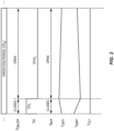
- Figure 2 illustrates an example operation of the voltage modulation circuit 16(1) for generating and maintain the modulated voltage V CC1 by toggling between a charge interval CH 1 and a discharge interval DCH 1 during an operation period OPx. Common elements between Figures 1 and 2 are shown therein with common element numbers and will not be re-described herein.
- the control circuit 30 closes the on-off switch S ON-OFF and the bypass switch S BYP such that the low-frequency current I DC1 can flow from the common node 28 through the offset capacitor C OFF1 and to the GND to thereby charge the offset capacitor C OFF1 to the offset voltage V OFF1 .
- the control circuit 30 activates the voltage amplifier 32(1) to generate the modulated initial voltage V AMP1 to help maintain the modulated voltage V CC1 at a desired level.
- the voltage modulation circuit 16(1) will enter the discharge interval DCH 1 .
- the control circuit 30 opens the on-off switch S ON-OFF and the bypass switch S BYP concurrently. In this regard, the low-frequency current loci is blocked from the common node and the offset capacitor C OFF1 is gradually discharged to maintain the modulated voltage V CC1 at the desired level.
- the voltage amplifier 32(1) may gradually reduce the modulated initial voltage V AMP1 as the offset capacitor C OFF1 is charged to gradually increase the offset voltage V OFF1 .
- the offset voltage V OFF1 will gradually decrease as the offset capacitor C OFF1 is discharged. Accordingly, the voltage amplifier 32(1) may gradually increase the modulated initial voltage V AMP1 .
- the voltage modulation circuit 16(1) can maintain the modulated voltage V CC1 consistently at the desired level.
- the voltage amplifier 32(1) may source or sink the high-frequency current I AMP1 to help charge or discharge a holding capacitor (not shown) in the load circuit 20(1) to thereby help maintain the modulated voltage V CC1 at the desired level.
- the voltage amplifier 32(1) will generate the sense current I SENSE1 to indicate the high-frequency current I AMP1 that is sourced or sunk by the voltage amplifier 32(1).
- each of the voltage modulation circuits 16(2)-16(N) can be configured to generate and maintain a respective one of the modulated voltages V CC2 -V CCN by toggling repeatedly between a respective charge interval and a respective discharge interval as described above in the example of the voltage modulation circuit 16(1).
- the control circuit 30 is configured to determine the respective charge interval and the respective discharge interval for each of the voltage modulation circuits 16(1)-16(N) such that the voltage modulation circuits 16(1)-16(N) can share the current modulation circuit 14 on a time-division basis.
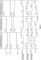
- Figure 3 provides an example illustration of a time-division operation among the voltage modulation circuits 16(1)-16(N) in Figure 1 . Common elements between Figures 1 and 3 are shown therein with common element numbers and will not be re-described herein.
- the time-division operation is repeated in each of one or more operation periods OP X-1 , OP X , OP X+1 .
- the operation periods OP X-1 , OP X , OP X+1 are merely examples for the purpose of illustration. It should be appreciated that the time-division operation can be repeated over any number of operation periods as needed.
- the control circuit 30 determines multiple charge intervals CH 1 -CH N and multiple discharge intervals DCH 1 -DCH N for the voltage modulation circuits 16(1)-16(N), respectively. As shown in Figure 3 , the charge intervals CH 1 -CH N are so determined not to overlap with one another. In contrast, the discharge intervals DCH 1 -DCH N may overlap with one another.
- the charge intervals CH 1 -CH N can be of equal duration or different durations, depending on whether the offset capacitors C OFF1 -C OFFN are having an identical capacitance or different capacitances. Specifically, when the offset capacitors C OFF1 -C OFFN are having the identical capacitance, the charge intervals CH 1 -CH N can have an identical duration. In contrast, when the offset capacitors C OFF1 -C OFFN are having different capacitances, the charge intervals CH 1 -CH N can have different durations. Regardless, a total duration of the charge intervals CH 1 -CH N shall be less than or equal to the duration of the operation period OPx.
- each of the voltage modulation circuits 16(1)-16(N) toggles between a respective one of the charge intervals CH 1 -CH N and a respective one of the discharge intervals DCH 1 -DCH N to generate and maintain a respective one of the modulated voltages V CC1 -V CCN .
- the voltage modulation circuits 16(1)-16(N) can make the modulated voltages V CC1 -V CCN concurrently available to enable simultaneous operations of the load circuits 20(1)-20(N), despite operating based on the time-division scheme.
- the control circuit 30 needs to adjust the duty cycles 26(1)-26(N) accordingly for each of the voltage modulation circuits 16(1)-16(N).
- the control circuit 30 may determine the duty cycles 26(1)-26(N) for a respective one of the voltage modulation circuits 16(1)-16(N) based on one or more of: a respective one of the modulated initial voltages V AMP1 -V AMPN , a respective one of the offset voltages V OFF1 -V OFFN , a respective one of the modulated voltages V CC1 -V CCN , and a respective one of the sense currents I SENSE1 -I SENSEN .
- Figure 4 is a schematic diagram providing an example illustration of the control circuit 30 in Figure 1 configured according to an embodiment of the present disclosure. Common elements between Figures 1 and 4 are shown therein with common element numbers and will not be re-described herein.
- control circuit 30 includes a first multiplexer 40, a second multiplexer 42, a third multiplexer 44, a fourth multiplexer 46, a first combiner 48, a second combiner 50, a third combiner 52, a controller 54, and a loop filter 56.
- the first multiplexer 40 When determining a respective one of the duty cycles 26(1)-26(N) for a respective one of the voltage modulation circuits 16(1)-16(N), the first multiplexer 40 outputs a respective one of the modulated initial voltages V AMP1 -V AMPN , the second multiplexer 42 outputs a respective one of the modulated voltages V CC1 -V CCN , the third multiplexer 44 outputs a respective one of the offset voltages V OFF1 -V OFFN , and the fourth multiplexer 46 outputs a respective one of the sense currents I SENSE1 -I SENSEN .
- the first combiner 48 combines the respective one of the modulated initial voltages V AMP1 -V AMPN and the respective one of the modulated voltages V CC1 -V CCN to output a first combined voltage V 1 .
- the second combiner 50 combines the first combined voltage V 1 with the respective one of the offset voltages V OFF1 -V OFFN to output a second voltage V 2 .
- the loop filter 56 is configured to convert the second voltage V 2 into a first current I 1 , which is combined with the respective one of the sense currents I SENSE1 -I SENSEN at the third combiner 52 to generate a combined current I COMB .
- the controller 54 which can be a bang-bang controller as an example, can then determine the respective one of the duty cycles 26(1)-26(N) for the respective one of the voltage modulation circuits 16(1)-16(N) based on the combined current I COMB .
- the current modulation circuit 14 needs to adapt the low-frequency currents I DC1 -I DCN accordingly in each of the operation periods OP X-1 , OP X , OP X+1 , and so on. As such, it is desirable to minimize an amount of current change (increase or decrease) between each of the low-frequency currents I DC1 -I DCN to help improve efficiency of the current modulation circuit 14.
- control circuit 30 can further include a scheduling circuit 58 to determine an order (also referred to as "current generation order") for generating the low-frequency currents I DC1 -I DCN in each of the operation periods OP X-1 , OP X , OP X+1 , and so on. Accordingly, the control circuit 30 can determine the duty cycles 26(1)-26(N) according to the determined current generation order to thereby cause the current modulation circuit 14 to generate the low-frequency currents I DC1 -I DCN according to the determined current generation order.
- a scheduling circuit 58 to determine an order (also referred to as "current generation order") for generating the low-frequency currents I DC1 -I DCN in each of the operation periods OP X-1 , OP X , OP X+1 , and so on. Accordingly, the control circuit 30 can determine the duty cycles 26(1)-26(N) according to the determined current generation order to thereby cause the current modulation circuit 14 to generate the low-frequency currents I DC1 -I
- the scheduling circuit 58 can control the first multiplexer 40, the second multiplexer 42, the third multiplexer 44, and the fourth multiplexer 46 via a selection signal 60.
- the scheduling circuit 58 can cause the modulated initial voltages V AMP1 -V AMPN , the modulated voltages V CC1 -V CCN , the offset voltages V OFF1 -V OFFN , and the sense currents I SENSE1 -I SENSEN to be outputted from the first multiplexer 40, the second multiplexer 42, the third multiplexer 44, and the fourth multiplexer 46 in accordance with the determined current generation order. Accordingly, the control circuit 30 can generate the duty cycles 26(1)-26(N) in accordance with the determined current generation order.
- the scheduling circuit 58 is configured to determine the current generation order (e.g., based on the modulated target voltages V TGT1 -V TGTN ) to minimize a relative change between each of the low-frequency currents I DC1 -I DCN in each of the operation periods OP X-1 , OP X , OP X+1 , and so on.
- Figure 5 provides an example illustration as to how the control circuit 30 in Figure 4 can determine the charge intervals CH 1 -CH N and the discharge intervals DCH 1 -DCH N in Figure 3 based on the determined current generation order.
- Figure 5 is described with reference to the voltage modulation circuits 16(1)-16(3) among the voltage modulation circuits 16(1)-16(N).
- the scheduling circuit 58 receives the modulated target voltages V TGT1 , V TGT2 , and V TGT3 that indicate changes of the modulated voltages V CC1 , V CC2 , and V CC3 in the operation period OP X-1 relative to what were in a prior operation period (e.g., OP X-2 ) are ⁇ V 1(X-1) , ⁇ V 2(X-1) , and ⁇ V 3(X-1) , respectively.
- the scheduling circuit 58 further determines that ⁇ V 2(X-1) ⁇ ⁇ V 3(X-1) ⁇ ⁇ V 1(X-1) .
- the scheduling circuit 58 can determine the current generation order in the operation period OP X-1 to be I DC2 , I DC3 , and I DC1 .
- the control circuit 30 will generate the duty cycles 26(2), 26(3), and 26(1) to cause the current modulation circuit 14 to generate the low-frequency currents I DC2 , I DC3 , and I DC1 , respectively.
- the control circuit 30 will also determine the charge intervals CH 2 , CH 3 , and CH 1 in the operation period OP X-1 for charging the offset capacitors C OFF2 , C OFF3 , and C OFF1 , respectively.
- the control circuit 30 can further determine the discharge intervals DCH 2 , DCH 3 , and DCH 1 accordingly.
- the scheduling circuit 58 receives the modulated target voltages V TGT1 , V TGT2 , and V TGT3 that indicate changes of the modulated voltages V CC1 , V CC2 , and V CC3 in the operation period OPx relative to what were in a prior operation period (e.g., OP X-1 ) are ⁇ V 1(X) , ⁇ V 2(X) , and ⁇ V 3(X) , respectively.
- the scheduling circuit 58 further determines that ⁇ V 1(X) ⁇ ⁇ V 3(X) ⁇ ⁇ V 2(X) .
- the scheduling circuit 58 can determine the current generation order in the operation period OPx to be I DC1 , I DC3 , and I DC2 .
- the control circuit 30 will generate the duty cycles 26(1), 26(3), and 26(2) to cause the current modulation circuit 14 to generate the low-frequency currents I DC1 , I DC3 , and I DC2 , respectively.
- the control circuit 30 will also determine the charge intervals CH 1 , CH 3 , and CH 2 in the operation period OPx for charging the offset capacitors C OFF1 , C OFF3 , and C OFF2 , respectively.
- the control circuit 30 can further determine the discharge intervals DCH 1 , DCH 3 , and DCH 2 accordingly.
- the scheduling circuit 58 receives the modulated target voltages V TGT1 , V TGT2 , and V TGT3 that indicate changes of the modulated voltages V CC1 , V CC2 , and V CC3 in the operation period OP X+1 relative to what were in a prior operation period (e.g., OP X ) are ⁇ V 1(X+1) , ⁇ V 2(X+1) , and ⁇ V 3(X+1) , respectively.
- the scheduling circuit 58 further determines that ⁇ V 3(X+1) ⁇ ⁇ V 2(X+1) ⁇ ⁇ V 1(X+1) .
- the scheduling circuit 58 can determine the current generation order in the operation period OP X+1 to be I DC3 , I DC2 , and I DC1 .
- the control circuit 30 will generate the duty cycles 26(3), 26(2), and 26(1) to cause the current modulation circuit 14 to generate the low-frequency currents I DC3 , I DC2 , and I DC1 , respectively.
- the control circuit 30 will also determine the charge intervals CH 3 , CH 2 , and CH 1 in the operation period OP X+1 for charging the offset capacitors C OFF3 , C OFF2 , and C OFF1 , respectively.
- the control circuit 30 can further determine the discharge intervals DCH 3 , DCH 2 , and DCH 1 accordingly.
- the multi-voltage generation circuit 12 in Figure 2 can be configured to generate the low-frequency currents I DC1 -I DCN according to a process.
- Figure 6 is a flowchart of an example process 200 for generating the low-frequency currents I DC1 -I DCN to cause the multi-voltage generation circuit 12 in Figure 1 to generate and maintain the modulated voltages V CC1 -V CCN .
- control circuit 30 is configured to determine an order (a.k.a. current generation order) for generating the low-frequency currents I DC1 -I DCN in the operation periods OP X-1 , OP X , OP X+1 , and so on (step 202). Accordingly, the current modulation circuit 14 can generate the low-frequency currents I DC1 -I DCN in each of the operation periods OP X-1 , OP X , OP X+1 , and so on according to the determined current generation order (step 204).
- an order a.k.a. current generation order
- the multi-voltage generation circuit includes multiple voltage modulation circuits that are configured to generate and maintain multiple modulated voltages.
- the multiple modulated voltages can be used for amplifying multiple radio frequency (RF) signals concurrently.
- the voltage modulation circuits are configured to share a single current modulation circuit based on time-division. By sharing a single current modulation circuit among the multiple voltage modulation circuits, it is possible to concurrently support multiple load circuits (e.g., power amplifier circuits) with significantly reduced footprint.
Landscapes
- Engineering & Computer Science (AREA)
- Power Engineering (AREA)
- Microelectronics & Electronic Packaging (AREA)
- Physics & Mathematics (AREA)
- Electromagnetism (AREA)
- General Physics & Mathematics (AREA)
- Radar, Positioning & Navigation (AREA)
- Automation & Control Theory (AREA)
- Amplifiers (AREA)
Abstract
Description
- This application claims the benefit of provisional patent application serial number
63/255,651, filed October 14, 2021 63/255,649, filed October 14, 2021 - The present disclosure is related to a power management circuit operable to maintain multiple voltages simultaneously.
- Mobile communication devices have become increasingly common in current society for providing wireless communication services. The prevalence of these mobile communication devices is driven in part by the many functions that are now enabled on such devices. Increased processing capabilities in such devices means that mobile communication devices have evolved from being pure communication tools into sophisticated mobile multimedia centers that enable enhanced user experiences.
- The redefined user experience requires higher data rates offered by such advanced wireless communication technologies as fifth-generation new-radio (5G-NR). To achieve higher data rates, a mobile communication device may employ a power amplifier(s) to amplify a radio frequency (RF) signal(s) (e.g., maintaining sufficient energy per bit) before transmission. Given that the power amplifier(s) requires a supply voltage(s) for operation, a power management integrated circuit (PMIC) is thus required to generate and provide the supply voltage(s) to the power amplifier(s).
- Given that the PMIC often needs to concurrently generate multiple supply voltages for multiple power amplifiers, the PMIC typically includes multiple direct-current to direct-current (DC-DC) converters for modulating the multiple supply voltages. Having the multiple DC-DC converters will inevitably increase footprint of the PMIC, thus making it difficult to fit the PMIC into an increasing miniaturized electronic device(s) such as a smartphone and smart gadgets. Hence, it is desirable to reduce the number of DC-DC converters in the PMIC to help reduce the footprint of the PMIC.
- Particular embodiments are set out in the independent claims. Various optional examples are set out in the dependent claims. Embodiments of the disclosure relate to a multi-voltage generation circuit. More specifically, the multi-voltage generation circuit includes multiple voltage modulation circuits that are configured to generate and maintain multiple modulated voltages. In a non-limiting example, the multiple modulated voltages can be used for amplifying multiple radio frequency (RF) signals concurrently. Contrary to using multiple direct-current (DC) to DC (DC-DC) converters for generating the multiple modulated voltages, the voltage modulation circuits are configured to share a single current modulation circuit based on time-division. By sharing a single current modulation circuit among the multiple voltage modulation circuits, it is possible to concurrently support multiple load circuits (e.g., power amplifier circuits) with significantly reduced footprint.
- In one aspect, a multi-voltage generation circuit is provided. The multi-voltage generation circuit includes a current modulation circuit configured to generate multiple low-frequency currents. The multi-voltage generation circuit also includes multiple voltage modulation circuits. Each of the multiple voltage modulation circuits includes a respective one of multiple voltage amplifiers configured to generate a respective one of multiple modulated initial voltages based on a respective one of multiple modulated target voltages. Each of the multiple voltage modulation circuits also includes a respective one of multiple offset capacitors each modulated to a respective one of multiple offset voltages by a respective one of the multiple low-frequency currents such that the respective one of the multiple offset voltages can raise the respective one of the multiple modulated initial voltages to thereby generate a respective one of multiple modulated voltages. The multi-voltage generation circuit also includes a control circuit. The control circuit is configured to determine an order for generating the multiple low-frequency currents in one or more operation periods. The control circuit is also configured to cause the current modulation circuit to generate the multiple low-frequency currents in each of the one or more operation periods according to the determined order.
- In another aspect, a method for generating multiple low-frequency currents is provided. The method includes determining an order for generating multiple low-frequency currents in one or more operation periods. The method also includes generating the multiple low-frequency currents in each of the one or more operation periods according to the determined current generation order.
- In another aspect, a multi-voltage power management circuit is provided. The multi-voltage power management circuit includes multiple power amplifier circuits. The multiple power amplifier circuits are configured to concurrently amplify multiple radio frequency (RF) signals based on multiple modulated voltages, respectively. The multi-voltage power management circuit also includes a multi-voltage generation circuit. The multi-voltage generation circuit includes a current modulation circuit configured to generate multiple low-frequency currents. The multi-voltage generation circuit also includes multiple voltage modulation circuits. Each of the multiple voltage modulation circuits includes a respective one of multiple voltage amplifiers configured to generate a respective one of multiple modulated initial voltages based on a respective one of multiple modulated target voltages. Each of the multiple voltage modulation circuits also includes a respective one of multiple offset capacitors each modulated to a respective one of multiple offset voltages by a respective one of the multiple low-frequency currents such that the respective one of the multiple offset voltages can raise the respective one of the multiple modulated initial voltages to thereby generate a respective one of the multiple modulated voltages. The multi-voltage generation circuit also includes a control circuit. The control circuit is configured to determine an order for generating the multiple low-frequency currents in one or more operation periods. The control circuit is also configured to cause the current modulation circuit to generate the plurality of low-frequency currents in each of the one or more operation periods according to the determined order.
- Those skilled in the art will appreciate the scope of the present disclosure and realize additional aspects thereof after reading the following detailed description of the preferred embodiments in association with the accompanying drawing figures.
- The accompanying drawing figures incorporated in and forming a part of this specification illustrate several aspects of the disclosure, and together with the description serve to explain the principles of the disclosure.
-
Figure 1 is a schematic diagram of an example multi-voltage power management circuit wherein a multi-voltage generation circuit is configured according to embodiments of the present disclosure to concurrently generate and maintain multiple modulated voltages by sharing a current modulation circuit; -
Figure 2 illustrates an example operation of a voltage modulation circuit for generating and maintaining any one of the multiple modulated voltages during an operation period(s); -
Figure 3 provides an example illustration of a time-division scheme that can be employed by the multi-voltage generation circuit inFigure 1 for concurrently generating and maintaining the multiple modulated voltages; -
Figure 4 is a schematic diagram of an example control circuit that can be provided in the multi-voltage generation circuit inFigure 1 for generating and maintaining the multiple modulated voltages concurrently; -
Figure 5 provides an example illustration as to how the control circuit inFigure 4 can determine the time-division scheme inFigure 3 based on a current generation order; and -
Figure 6 is a flowchart of an example process for generating multiple low-frequency currents to cause the multi-voltage generation circuit inFigure 1 to generate and maintain the modulated voltages. - The embodiments set forth below represent the necessary information to enable those skilled in the art to practice the embodiments and illustrate the best mode of practicing the embodiments. Upon reading the following description in light of the accompanying drawing figures, those skilled in the art will understand the concepts of the disclosure and will recognize applications of these concepts not particularly addressed herein. It should be understood that these concepts and applications fall within the scope of the disclosure and the accompanying claims.
- It will be understood that, although the terms first, second, etc. may be used herein to describe various elements, these elements should not be limited by these terms. These terms are only used to distinguish one element from another. For example, a first element could be termed a second element, and, similarly, a second element could be termed a first element, without departing from the scope of the present disclosure. As used herein, the term "and/or" includes any and all combinations of one or more of the associated listed items.
- It will be understood that when an element such as a layer, region, or substrate is referred to as being "on" or extending "onto" another element, it can be directly on or extend directly onto the other element or intervening elements may also be present. In contrast, when an element is referred to as being "directly on" or extending "directly onto" another element, there are no intervening elements present. Likewise, it will be understood that when an element such as a layer, region, or substrate is referred to as being "over" or extending "over" another element, it can be directly over or extend directly over the other element or intervening elements may also be present. In contrast, when an element is referred to as being "directly over" or extending "directly over" another element, there are no intervening elements present. It will also be understood that when an element is referred to as being "connected" or "coupled" to another element, it can be directly connected or coupled to the other element or intervening elements may be present. In contrast, when an element is referred to as being "directly connected" or "directly coupled" to another element, there are no intervening elements present.
- Relative terms such as "below" or "above" or "upper" or "lower" or "horizontal" or "vertical" may be used herein to describe a relationship of one element, layer, or region to another element, layer, or region as illustrated in the Figures. It will be understood that these terms and those discussed above are intended to encompass different orientations of the device in addition to the orientation depicted in the Figures.
- The terminology used herein is for the purpose of describing particular embodiments only and is not intended to be limiting of the disclosure. As used herein, the singular forms "a," "an," and "the" are intended to include the plural forms as well, unless the context clearly indicates otherwise. It will be further understood that the terms "comprises," "comprising," "includes," and/or "including" when used herein specify the presence of stated features, integers, steps, operations, elements, and/or components, but do not preclude the presence or addition of one or more other features, integers, steps, operations, elements, components, and/or groups thereof.
- Unless otherwise defined, all terms (including technical and scientific terms) used herein have the same meaning as commonly understood by one of ordinary skill in the art to which this disclosure belongs. It will be further understood that terms used herein should be interpreted as having a meaning that is consistent with their meaning in the context of this specification and the relevant art and will not be interpreted in an idealized or overly formal sense unless expressly so defined herein.
- Embodiments are described herein with reference to a multi-voltage generation circuit. More specifically, the multi-voltage generation circuit includes multiple voltage modulation circuits that are configured to generate and maintain multiple modulated voltages. In a non-limiting example, the multiple modulated voltage can be used for amplifying multiple radio frequency (RF) signals concurrently. Contrary to using multiple direct-current (DC) to DC (DC-DC) converters for generating the multiple modulated voltages, the voltage modulation circuits are configured to share a single current modulation circuit based on time-division. By sharing a single current modulation circuit among the multiple voltage modulation circuits, it is possible to concurrently support multiple load circuits (e.g., power amplifier circuits) with significantly reduced footprint.
- In this regard,
Figure 1 is a schematic diagram of an example multi-voltagepower management circuit 10 wherein amulti-voltage generation circuit 12 is configured according to embodiments of the present disclosure to concurrently generate and maintain multiple modulated voltages VCC1-VCCN by sharing acurrent modulation circuit 14. Herein, themulti-voltage generation circuit 12 includes multiple voltage modulation circuits 16(1)-16(N) each configured to share thecurrent modulation circuit 14 based on time-division to thereby generate and maintain a respective one of the modulated voltages VCC1-VCCN. The voltage modulation circuits 16(1)-16(N) are configured to output the modulated voltages VCC1-VCCN via multiple voltage outputs 18(1)-18(N), respectively. - In an embodiment, the voltage outputs 18(1)-18(N) are coupled to multiple load circuits 20(1)-20(N), respectively. In this regard, the voltage modulation circuits 16(1)-16(N) are configured to concurrently provide and maintain the modulated voltages VCC1-VCCN for the load circuits 20(1)-20(N). In a non-limiting example, the load circuits 20(1)-20(N) can be power amplifier circuits each configured to amplify a respective one of multiple RF signals (not shown) based on a respective one of the modulated voltages VCC1-VCCN. Understandably, the load circuits 20(1)-20(N) can also be any other active circuits that operate based on a voltage. Further, the load circuits 20(1)-20(N) may also include a mixture of power amplifier circuits and other types of active circuits. By sharing the
current modulation circuit 14 among the voltage modulation circuits 16(1)-16(N), the multi-voltagepower management circuit 10 can concurrently support the load circuits 20(1)-20(N) with significantly reduced footprint. - According to an embodiment of the present disclosure, the
current modulation circuit 14 includes a multi-level charge pump (MCP) 22 and apower inductor 24. TheMCP 22 is configured to operate based on a plurality of duty cycles 26(1)-26(N) to generate a plurality of low-frequency voltages VDC1-VDCN (e.g., DC voltages), each as a function of a battery voltage VBAT. In a non-limiting example, theMCP 22 can be a DC-DC buck-boost converter that can operate in a buck mode and/or a boost mode. Herein, theMCP 22 is configured to generate each of the low-frequency voltages VDC1-VDCN at 0×VBAT or 1×VBAT when operating in the buck mode, or at 2×VBAT when operating in the boost mode. Understandably, theMCP 22 can toggle between 0×VBAT, 1×VBA, and/or 2×VBAT based on a respective one of the duty cycles 26(1)-26(N) to thereby generate each of the low-frequency voltages VDC1-VDCN at any desired voltage level. In other words, it is possible to adjust the low-frequency voltages VDC1-VDCN by simply adjusting the duty cycles 26(1)-26(N). - The
power inductor 24 is coupled between theMCP 22 and acommon node 28. Herein, thepower inductor 24 is configured to induce a multiple low-frequency current IDC1-IDCN (e.g., a DC current) based on the low-frequency voltages VDC1-VDCN, respectively. Given that the low-frequency voltages VDC1-VDCN can be adjusted based on the duty cycles 26(1)-26(N), the low-frequency currents IDC1-IDCN can likewise be adjusted based on the duty cycles 26(1)-26(N). - In an embodiment, the
multi-voltage generation circuit 12 further includes acontrol circuit 30, which can be a field-programmable gate array (FPGA) or an application-specific integrated circuit (ASIC), as an example. As further discussed inFigure 4 , thecontrol circuit 30 can be configured to adjust each of the duty cycles 26(1)-26(N) based on a variety of feedback provided by the voltage modulation circuits 16(1)-16(N). In addition, thecontrol circuit 30 is further configured to determine a time-division schedule whereby the voltage modulation circuits 16(1)-16(N) can share thecurrent modulation circuit 14. - In an embodiment, each of the voltage modulation circuits 16(1)-16(N) includes a respective one of multiple voltage amplifiers 32(1)-32(N), a respective one of multiple offset capacitors COFF1-COFFN, a respective bypass switch SBYP, and a respective on-off switch SON-OFF. In a non-limiting example, the
control circuit 30 can control (e.g., toggle) the bypass switch SBYP and the on-off switch SON-OFF in each of the voltage modulation circuits 16(1)-16(N) via a respective one of multiple control signals 34(1)-34(N). - Each of the voltage amplifiers 32(1)-32(N) is configured to generate a respective one of multiple modulated initial voltages VAMP1-VAMPN at a respective one of multiple outputs 36(1)-36(N) based on a respective one of multiple modulated target voltages VTGT1-VTGTN and a respective one of multiple supply voltages VSUP1-VSUPN. For example, the voltage amplifier 32(1) generates the modulated initial voltage VAMP1 at the output 36(1) of the voltage amplifier 32(1) based on the modulated target voltage VTGT1 and the supply voltage VSUP1, and the voltage amplifier 32(N) generates the modulated initial voltage VAMPN at the output 36(N) of the voltage amplifier 32(N) based on the modulated target voltage VTGTN and the supply voltage VSUPN.
- In an embodiment, each of the voltage amplifiers 32(1)-32(N) may be configured to source or sink a respective one of multiple high-frequency current IAMP1-IAMPN (e.g., alternating currents) to help maintain a respective one of the modulated voltages VCC1-VCCN at a desired level. In this regard, each of the voltage amplifiers 32(1)-32(N) may generate a respective one of multiple sense currents ISENSE1-ISENSEN to indicate an amount of the respective one of the high-frequency current IAMP1-IAMPN that is sourced or sunk by the respective one of the voltage amplifiers 32(1)-32(N).
- Each of the offset capacitors COFF1-COFFN is coupled between a respective one of the outputs 36(1)-36(N) and a respective one of the voltage outputs 18(1)-18(N). For example, the offset capacitor COFF1 is coupled between the output 36(1) of the voltage amplifier 32(1) and the voltage output 18(1) of the voltage modulation circuit 16(1), and the offset capacitor COFFN is coupled between the output 36(N) of the voltage amplifier 32(N) and the voltage output 18(N) of the voltage modulation circuit 16(N). Each of the offset capacitors COFF1-COFFN is configured to raise a respective one of the modulated voltages VAMP1-VAMPN by a respective one of multiple offset voltages VOFF1-VOFFN to thereby generate a respective one of the modulated voltages VCC1-VCCN at a respective one of the voltage outputs 18(1)-18(N). For example, the offset capacitor COFF1 is configured to raise the modulated initial voltage VAMP1 by the offset voltage VOFF1 to thereby generate the modulated voltage VCC1 (VCC1 = VAMP1 + VOFF1) at the voltage output 18(1), and the offset capacitor COFFN is configured to raise the modulated initial voltage VAMPN by the offset voltage VOFFN to thereby generate the modulated voltage VCCN (VCCN = VAMPN + VOFFN) at the voltage output 18(N).
- In one embodiment, the offset capacitors COFF1-COFFN can be configured to have an identical capacitance. In an alternative embodiment, the offset capacitors COFF1-COFFN can also be configured to have different capacitances. Further, the offset capacitors COFF1-COFFN can also be a same type or different types of capacitors.
- The bypass switch SBYP in each of the voltage modulation circuits 16(1)-16(N) is coupled between a respective one of the outputs 36(1)-36(N) and a ground (GND). For example, the bypass switch SBYP in the voltage modulation circuit 16(1) is coupled between the output 36(1) of the voltage amplifier 32(1) and the GND, and the bypass switch SBYP in the voltage modulation circuit 16(N) is coupled between the output 36(N) of the voltage amplifier 32(N) and the GND.
- The on-off switch SON-OFF in each of the voltage modulation circuits 16(1)-16(N) is coupled between the
common node 28 and a respective one of the voltage outputs 18(1)-18(N). For example, the on-off switch SON-OFF in the voltage modulation circuit 16(1) is coupled between thecommon node 28 and the voltage output 18(1) of the voltage modulation circuit 16(1), and the on-off switch SON-OFF in the voltage modulation circuit 16(N) is coupled between thecommon node 28 and the voltage output 18(N) of the voltage modulation circuit 16(N). - In an embodiment, the on-off switch SON-OFF in each of the voltage modulation circuits 16(1)-16(N) can be closed to provide a respective one of the low-frequency currents IDC1-IDCN from the
common node 28 to a respective one of the voltage outputs 18(1)-18(N). In contrast, the on-off switch SON-OFF in each of the voltage modulation circuits 16(1)-16(N) can be opened to prevent the respective one of the low-frequency currents IDC1-IDCN from flowing from thecommon node 28 to the respective one of the voltage outputs 18(1)-18(N). - Each of the voltage modulation circuits 16(1)-16(N) further includes a respective one of multiple voltage feedback paths 38(1)-38(N). Each of the voltage feedback paths 38(1)-38(N) is configured to provide a respective one of multiple modulated voltage feedbacks VCC-FB1-VCC-FBN from a respective one of the voltage outputs 18(1)-18(N) to a respective input of the voltage amplifiers 32(1)-32(N). In this regard, each of the voltage modulation circuits 16(1)-16(N) is a closed-loop voltage modulation circuit.
- Each of the voltage modulation circuits 16(1)-16(N) can be configured to generate and maintain a respective one of the modulated voltages VCC1-VCCN based on operations described below. Herein, operations of the voltage modulation circuit 16(1) are discussed as a non-limiting example. Understandably, the operation principles described with reference to the voltage modulation circuit 16(1) are applicable to any of the voltage modulation circuits 16(1)-16(N).
- In essence, the voltage modulation circuit 16(1) can be configured to generate and maintain the modulated voltage VCC1 by toggling repeatedly between a charge interval and a discharge interval.
Figure 2 illustrates an example operation of the voltage modulation circuit 16(1) for generating and maintain the modulated voltage VCC1 by toggling between a charge interval CH1 and a discharge interval DCH1 during an operation period OPx. Common elements betweenFigures 1 and2 are shown therein with common element numbers and will not be re-described herein. - During the charge interval CH1, the
control circuit 30 closes the on-off switch SON-OFF and the bypass switch SBYP such that the low-frequency current IDC1 can flow from thecommon node 28 through the offset capacitor COFF1 and to the GND to thereby charge the offset capacitor COFF1 to the offset voltage VOFF1. While the offset capacitor COFF is being charged, thecontrol circuit 30 activates the voltage amplifier 32(1) to generate the modulated initial voltage VAMP1 to help maintain the modulated voltage VCC1 at a desired level. - Once the offset capacitor COFF1 is charged up to the offset voltage VOFF1, the voltage modulation circuit 16(1) will enter the discharge interval DCH1. During the discharge interval DCH1, the
control circuit 30 opens the on-off switch SON-OFF and the bypass switch SBYP concurrently. In this regard, the low-frequency current loci is blocked from the common node and the offset capacitor COFF1 is gradually discharged to maintain the modulated voltage VCC1 at the desired level. - As shown in
Figure 2 , during the charge interval CH1, the voltage amplifier 32(1) may gradually reduce the modulated initial voltage VAMP1 as the offset capacitor COFF1 is charged to gradually increase the offset voltage VOFF1. In contrast, during the discharge interval DCH1, the offset voltage VOFF1 will gradually decrease as the offset capacitor COFF1 is discharged. Accordingly, the voltage amplifier 32(1) may gradually increase the modulated initial voltage VAMP1. As such, the voltage modulation circuit 16(1) can maintain the modulated voltage VCC1 consistently at the desired level. - In an embodiment, the voltage amplifier 32(1) may source or sink the high-frequency current IAMP1 to help charge or discharge a holding capacitor (not shown) in the load circuit 20(1) to thereby help maintain the modulated voltage VCC1 at the desired level. In this regard, the voltage amplifier 32(1) will generate the sense current ISENSE1 to indicate the high-frequency current IAMP1 that is sourced or sunk by the voltage amplifier 32(1).
- With reference back to
Figure 1 , each of the voltage modulation circuits 16(2)-16(N) can be configured to generate and maintain a respective one of the modulated voltages VCC2-VCCN by toggling repeatedly between a respective charge interval and a respective discharge interval as described above in the example of the voltage modulation circuit 16(1). In this regard, thecontrol circuit 30 is configured to determine the respective charge interval and the respective discharge interval for each of the voltage modulation circuits 16(1)-16(N) such that the voltage modulation circuits 16(1)-16(N) can share thecurrent modulation circuit 14 on a time-division basis. -
Figure 3 provides an example illustration of a time-division operation among the voltage modulation circuits 16(1)-16(N) inFigure 1 . Common elements betweenFigures 1 and3 are shown therein with common element numbers and will not be re-described herein. - Notably, the time-division operation is repeated in each of one or more operation periods OPX-1, OPX, OPX+1. Notably, the operation periods OPX-1, OPX, OPX+1 are merely examples for the purpose of illustration. It should be appreciated that the time-division operation can be repeated over any number of operation periods as needed.
- Specifically, during the operation period OPX, the
control circuit 30 determines multiple charge intervals CH1-CHN and multiple discharge intervals DCH1-DCHN for the voltage modulation circuits 16(1)-16(N), respectively. As shown inFigure 3 , the charge intervals CH1-CHN are so determined not to overlap with one another. In contrast, the discharge intervals DCH1-DCHN may overlap with one another. - The charge intervals CH1-CHN can be of equal duration or different durations, depending on whether the offset capacitors COFF1-COFFN are having an identical capacitance or different capacitances. Specifically, when the offset capacitors COFF1-COFFN are having the identical capacitance, the charge intervals CH1-CHN can have an identical duration. In contrast, when the offset capacitors COFF1-COFFN are having different capacitances, the charge intervals CH1-CHN can have different durations. Regardless, a total duration of the charge intervals CH1-CHN shall be less than or equal to the duration of the operation period OPx.
- In this regard, each of the voltage modulation circuits 16(1)-16(N) toggles between a respective one of the charge intervals CH1-CHN and a respective one of the discharge intervals DCH1-DCHN to generate and maintain a respective one of the modulated voltages VCC1-VCCN. The voltage modulation circuits 16(1)-16(N) can make the modulated voltages VCC1-VCCN concurrently available to enable simultaneous operations of the load circuits 20(1)-20(N), despite operating based on the time-division scheme.
- With reference back to
Figure 1 , since the modulated voltages VCC1-VCCN can be at different voltage levels, thecontrol circuit 30 needs to adjust the duty cycles 26(1)-26(N) accordingly for each of the voltage modulation circuits 16(1)-16(N). According to an embodiment of the present disclosure, thecontrol circuit 30 may determine the duty cycles 26(1)-26(N) for a respective one of the voltage modulation circuits 16(1)-16(N) based on one or more of: a respective one of the modulated initial voltages VAMP1-VAMPN, a respective one of the offset voltages VOFF1-VOFFN, a respective one of the modulated voltages VCC1-VCCN, and a respective one of the sense currents ISENSE1-ISENSEN. -
Figure 4 is a schematic diagram providing an example illustration of thecontrol circuit 30 inFigure 1 configured according to an embodiment of the present disclosure. Common elements betweenFigures 1 and4 are shown therein with common element numbers and will not be re-described herein. - Herein, the
control circuit 30 includes afirst multiplexer 40, asecond multiplexer 42, athird multiplexer 44, afourth multiplexer 46, afirst combiner 48, asecond combiner 50, athird combiner 52, acontroller 54, and aloop filter 56. - When determining a respective one of the duty cycles 26(1)-26(N) for a respective one of the voltage modulation circuits 16(1)-16(N), the
first multiplexer 40 outputs a respective one of the modulated initial voltages VAMP1-VAMPN, thesecond multiplexer 42 outputs a respective one of the modulated voltages VCC1-VCCN, thethird multiplexer 44 outputs a respective one of the offset voltages VOFF1-VOFFN, and thefourth multiplexer 46 outputs a respective one of the sense currents ISENSE1-ISENSEN. - The
first combiner 48 combines the respective one of the modulated initial voltages VAMP1-VAMPN and the respective one of the modulated voltages VCC1-VCCN to output a first combined voltage V1. Thesecond combiner 50 combines the first combined voltage V1 with the respective one of the offset voltages VOFF1-VOFFN to output a second voltage V2. Theloop filter 56 is configured to convert the second voltage V2 into a first current I1, which is combined with the respective one of the sense currents ISENSE1-ISENSEN at thethird combiner 52 to generate a combined current ICOMB. Thecontroller 54, which can be a bang-bang controller as an example, can then determine the respective one of the duty cycles 26(1)-26(N) for the respective one of the voltage modulation circuits 16(1)-16(N) based on the combined current ICOMB. - Notably, since the modulated voltages VCC1-VCCN can be different from one another in each of the operation periods OPX-1, OPX, OPX+1, and so on, the
current modulation circuit 14 needs to adapt the low-frequency currents IDC1-IDCN accordingly in each of the operation periods OPX-1, OPX, OPX+1, and so on. As such, it is desirable to minimize an amount of current change (increase or decrease) between each of the low-frequency currents IDC1-IDCN to help improve efficiency of thecurrent modulation circuit 14. - In this regard, the
control circuit 30 can further include ascheduling circuit 58 to determine an order (also referred to as "current generation order") for generating the low-frequency currents IDC1-IDCN in each of the operation periods OPX-1, OPX, OPX+1, and so on. Accordingly, thecontrol circuit 30 can determine the duty cycles 26(1)-26(N) according to the determined current generation order to thereby cause thecurrent modulation circuit 14 to generate the low-frequency currents IDC1-IDCN according to the determined current generation order. - In a non-limiting example, once the
scheduling circuit 58 determines the current generation order for a respective one of the operation periods OPX-1, OPX, OPX+1, and so on, thescheduling circuit 58 can control thefirst multiplexer 40, thesecond multiplexer 42, thethird multiplexer 44, and thefourth multiplexer 46 via aselection signal 60. As such, thescheduling circuit 58 can cause the modulated initial voltages VAMP1-VAMPN, the modulated voltages VCC1-VCCN, the offset voltages VOFF1-VOFFN, and the sense currents ISENSE1-ISENSEN to be outputted from thefirst multiplexer 40, thesecond multiplexer 42, thethird multiplexer 44, and thefourth multiplexer 46 in accordance with the determined current generation order. Accordingly, thecontrol circuit 30 can generate the duty cycles 26(1)-26(N) in accordance with the determined current generation order. - According to an embodiment of the present disclosure, the
scheduling circuit 58 is configured to determine the current generation order (e.g., based on the modulated target voltages VTGT1-VTGTN) to minimize a relative change between each of the low-frequency currents IDC1-IDCN in each of the operation periods OPX-1, OPX, OPX+1, and so on. In this regard,Figure 5 provides an example illustration as to how thecontrol circuit 30 inFigure 4 can determine the charge intervals CH1-CHN and the discharge intervals DCH1-DCHN inFigure 3 based on the determined current generation order. For the sake of illustration,Figure 5 is described with reference to the voltage modulation circuits 16(1)-16(3) among the voltage modulation circuits 16(1)-16(N). - In one example, the
scheduling circuit 58 receives the modulated target voltages VTGT1, VTGT2, and VTGT3 that indicate changes of the modulated voltages VCC1, VCC2, and VCC3 in the operation period OPX-1 relative to what were in a prior operation period (e.g., OPX-2) are ΔV1(X-1), ΔV2(X-1), and ΔV3(X-1), respectively. Thescheduling circuit 58 further determines that ΔV2(X-1) < ΔV3(X-1) < ΔV1(X-1). Accordingly, thescheduling circuit 58 can determine the current generation order in the operation period OPX-1 to be IDC2, IDC3, and IDC1. In this regard, thecontrol circuit 30 will generate the duty cycles 26(2), 26(3), and 26(1) to cause thecurrent modulation circuit 14 to generate the low-frequency currents IDC2, IDC3, and IDC1, respectively. Given the current generation order, thecontrol circuit 30 will also determine the charge intervals CH2, CH3, and CH1 in the operation period OPX-1 for charging the offset capacitors COFF2, COFF3, and COFF1, respectively. Upon determining the charge intervals CH2, CH3, and CH1, thecontrol circuit 30 can further determine the discharge intervals DCH2, DCH3, and DCH1 accordingly. - In another example, the
scheduling circuit 58 receives the modulated target voltages VTGT1, VTGT2, and VTGT3 that indicate changes of the modulated voltages VCC1, VCC2, and VCC3 in the operation period OPx relative to what were in a prior operation period (e.g., OPX-1) are ΔV1(X), ΔV2(X), and ΔV3(X), respectively. Thescheduling circuit 58 further determines that ΔV1(X) < ΔV3(X) < ΔV2(X). Accordingly, thescheduling circuit 58 can determine the current generation order in the operation period OPx to be IDC1, IDC3, and IDC2. In this regard, thecontrol circuit 30 will generate the duty cycles 26(1), 26(3), and 26(2) to cause thecurrent modulation circuit 14 to generate the low-frequency currents IDC1, IDC3, and IDC2, respectively. Given the current generation order, thecontrol circuit 30 will also determine the charge intervals CH1, CH3, and CH2 in the operation period OPx for charging the offset capacitors COFF1, COFF3, and COFF2, respectively. Upon determining the charge intervals CH1, CH3, and CH2, thecontrol circuit 30 can further determine the discharge intervals DCH1, DCH3, and DCH2 accordingly. - In another example, the
scheduling circuit 58 receives the modulated target voltages VTGT1, VTGT2, and VTGT3 that indicate changes of the modulated voltages VCC1, VCC2, and VCC3 in the operation period OPX+1 relative to what were in a prior operation period (e.g., OPX) are ΔV1(X+1), ΔV2(X+1), and ΔV3(X+1), respectively. Thescheduling circuit 58 further determines that ΔV3(X+1) < ΔV2(X+1) < ΔV1(X+1). Accordingly, thescheduling circuit 58 can determine the current generation order in the operation period OPX+1 to be IDC3, IDC2, and IDC1. In this regard, thecontrol circuit 30 will generate the duty cycles 26(3), 26(2), and 26(1) to cause thecurrent modulation circuit 14 to generate the low-frequency currents IDC3, IDC2, and IDC1, respectively. Given the current generation order, thecontrol circuit 30 will also determine the charge intervals CH3, CH2, and CH1 in the operation period OPX+1 for charging the offset capacitors COFF3, COFF2, and COFF1, respectively. Upon determining the charge intervals CH3, CH2, and CH1, thecontrol circuit 30 can further determine the discharge intervals DCH3, DCH2, and DCH1 accordingly. - The
multi-voltage generation circuit 12 inFigure 2 can be configured to generate the low-frequency currents IDC1-IDCN according to a process. In this regard,Figure 6 is a flowchart of anexample process 200 for generating the low-frequency currents IDC1-IDCN to cause themulti-voltage generation circuit 12 inFigure 1 to generate and maintain the modulated voltages VCC1-VCCN. - Herein, the
control circuit 30 is configured to determine an order (a.k.a. current generation order) for generating the low-frequency currents IDC1-IDCN in the operation periods OPX-1, OPX, OPX+1, and so on (step 202). Accordingly, thecurrent modulation circuit 14 can generate the low-frequency currents IDC1-IDCN in each of the operation periods OPX-1, OPX, OPX+1, and so on according to the determined current generation order (step 204). - Thus, from one perspective, there has now been described a multi-voltage power generation circuit. More specifically, the multi-voltage generation circuit includes multiple voltage modulation circuits that are configured to generate and maintain multiple modulated voltages. In a non-limiting example, the multiple modulated voltages can be used for amplifying multiple radio frequency (RF) signals concurrently. Contrary to using multiple direct-current (DC) to DC (DC-DC) converters for generating the multiple modulated voltages, the voltage modulation circuits are configured to share a single current modulation circuit based on time-division. By sharing a single current modulation circuit among the multiple voltage modulation circuits, it is possible to concurrently support multiple load circuits (e.g., power amplifier circuits) with significantly reduced footprint.
- Those skilled in the art will recognize improvements and modifications to the preferred embodiments of the present disclosure. All such improvements and modifications are considered within the scope of the concepts disclosed herein and the claims that follow.
- Further examples of feature combinations taught by the present disclosure are set out in the following numbered clauses:
- 1. A multi-voltage generation circuit comprising:
- a current modulation circuit configured to generate a plurality of low-frequency currents;
- a plurality of voltage modulation circuits each comprising:
- a respective one of a plurality of voltage amplifiers configured to generate a respective one of a plurality of modulated initial voltages based on a respective one of a plurality of modulated target voltages; and
- a respective one of a plurality of offset capacitors each modulated to a respective one of a plurality of offset voltages by a respective one of the plurality of low-frequency currents such that the respective one of the plurality of offset voltages can raise the respective one of the plurality of modulated initial voltages to thereby generate a respective one of a plurality of modulated voltages; and
- a control circuit configured to:
- determine an order for generating the plurality of low-frequency currents in one or more operation periods; and
- cause the current modulation circuit to generate the plurality of low-frequency currents in each of the one or more operation periods according to the determined order.
- 2. The multi-voltage generation circuit of
clause 1, wherein the control circuit is further configured to determine the order for generating the plurality of low-frequency currents to minimize a relative change between each of the plurality of low-frequency currents. - 3. The multi-voltage generation circuit of
clause 1 orclause 2, wherein the current modulation circuit comprises:- a multi-level charge pump (MCP) configured to operate based on a plurality of duty cycles to generate a plurality of low-frequency voltages each as a function of a battery voltage; and
- a power inductor coupled between the MCP and a common node and configured to induce the plurality of low-frequency currents based on the plurality of low-frequency voltages, respectively;
- wherein the control circuit is further configured to determine the plurality of duty cycles in accordance with the determined order for generating the plurality of low-frequency currents to thereby cause the current modulation circuit to generate the plurality of low-frequency currents in each of the one or more operation periods.
- 4. The multi-voltage generation circuit of
clause 3, wherein the control circuit is further configured to:- determine a plurality of charge intervals in each of the one or more operation periods in accordance with the determined order for generating the plurality of low-frequency currents; and
- cause each of the plurality of offset capacitors to be charged to the respective one of the plurality of offset voltages during a respective one of the plurality of charge intervals.
- 5. The multi-voltage generation circuit of clause 4, wherein the control circuit is further configured to:
- determine a plurality of discharge intervals each corresponding to a respective one of the plurality of charge intervals; and
- cause each of the plurality of offset capacitors to be discharged to maintain the respective one of the plurality of modulated voltages during a respective one of the plurality of discharge intervals.
- 6. The multi-voltage generation circuit of clause 5, wherein each of the plurality of voltage modulation circuits further comprises:
- a respective voltage output that outputs the respective one of the plurality of modulated voltages, wherein the respective one of the plurality of offset capacitors is coupled between a respective one of the respective one of the plurality of voltage amplifiers and the respective voltage output;
- a respective bypass switch coupled between the respective output of the respective one of the plurality of voltage amplifiers and a ground; and
- a respective on-off switch coupled between the power inductor and the respective voltage output.
- 7. The multi-voltage generation circuit of clause 6, wherein the control circuit is further configured to, for each of the plurality of voltage modulation circuits:
- close the respective on-off switch during the respective one of the plurality of charge intervals to provide a respective one of the plurality of low-frequency currents from the common node to the respective voltage output;
- close the respective bypass switch during the respective one of the plurality of charge intervals such that the respective one of the plurality of low-frequency currents can charge the respective one of the plurality of offset capacitors to the respective one of the plurality of offset voltages; and
- cause the respective one of the plurality of voltage amplifiers to source or sink a respective high-frequency current during the respective one of the plurality of charge intervals to thereby maintain the respective one of the plurality of modulated voltages.
- 8. The multi-voltage generation circuit of clause 7, wherein the control circuit is further configured to, for each of the plurality of voltage modulation circuits:
- open the respective on-off switch during the respective one of the plurality of discharge intervals to block the respective one of the plurality of low-frequency currents from flowing from the common node to the respective voltage output; and
- open the respective bypass switch during the respective one of the plurality of discharge intervals such that the respective one of the plurality of offset capacitors is discharged to maintain the respective one of the plurality of modulated voltages.
- 9. The multi-voltage generation circuit of clause 7 or clause 8, wherein each of the plurality of voltage amplifiers is further configured to generate a respective one of a plurality of sense currents indicating a respective amount of the high-frequency current that is sourced/sunk by the respective one of the plurality of voltage amplifiers during the respective one of the plurality of charge intervals.
- 10. The multi-voltage generation circuit of clause 9, wherein the control circuit is further configured to determine each of the plurality of duty cycles based on one or more of:
- the respective one of the plurality of modulated initial voltages;
- the respective one of the plurality of offset voltages;
- the respective one of the plurality of modulated voltages; and
- the respective one of the plurality of sense currents.
- 11. A method for generating multiple low-frequency currents comprising:
- determining an order for generating a plurality of low-frequency currents in one or more operation periods; and
- generating the plurality of low-frequency currents in each of the one or more operation periods according to the determined current generation order.
- 12. The method of clause 11, further comprising determining the current generation order to minimize a relative change between each of the plurality of low-frequency currents.
- 13. The method of clause 11 or
clause 12, further comprising:- operating based on a plurality of duty cycles to generate a plurality of low-frequency voltages each as a function of a battery voltage;
- inducing the plurality of low-frequency currents based on the plurality of low-frequency voltages, respectively; and
- determining the plurality of duty cycles in accordance with the determined current generation in order to thereby generate the plurality of low-frequency currents in each of the one or more operation periods.
- 14. The method of clause 13, further comprising:
- determining a plurality of charge intervals in each of the one or more operation periods in accordance with the determined current generation order; and
- charging a plurality of offset capacitors in the plurality of charge intervals based on the plurality of low-frequency currents, respectively.
- 15. The method of
clause 14, further comprising:- determining a plurality of discharge intervals each corresponding to a respective one of the plurality of charge intervals; and
- discharging the plurality of offset capacitors in the plurality of discharge intervals, respectively.
- 16. A multi-voltage power management circuit comprising:
- a plurality of power amplifier circuits configured to concurrently amplify a plurality of radio frequency (RF) signals based on a plurality of modulated voltages, respectively; and
- a multi-voltage generation circuit comprising:
- a current modulation circuit configured to generate a plurality of low-frequency currents;
- a plurality of voltage modulation circuits each comprising:
- a respective one of a plurality of voltage amplifiers configured to generate a respective one of a plurality of modulated initial voltages based on a respective one of a plurality of modulated target voltages; and
- a respective one of a plurality of offset capacitors each modulated to a respective one of a plurality of offset voltages by a respective one of the plurality of low-frequency currents such that the respective one of the plurality of offset voltages can raise the respective one of the plurality of modulated initial voltages to thereby generate a respective one of the plurality of modulated voltages; and
- a control circuit configured to:
- determine an order for generating the plurality of low-frequency currents in one or more operation periods; and
- cause the current modulation circuit to generate the plurality of low-frequency currents in each of the one or more operation periods according to the determined order.
- 17. The multi-voltage power management circuit of
clause 16, wherein the control circuit is further configured to determine the order for generating the plurality of low-frequency currents to minimize a relative change between each of the plurality of low-frequency currents. - 18. The multi-voltage power management circuit of
clause 16 or clause 17, wherein the current modulation circuit comprises:- a multi-level charge pump (MCP) configured to operate based on a plurality of duty cycles to generate a plurality of low-frequency voltages each as a function of a battery voltage; and
- a power inductor coupled between the MCP and a common node and configured to induce the plurality of low-frequency currents based on the plurality of low-frequency voltages, respectively;
- wherein the control circuit is further configured to determine the plurality of duty cycles in accordance with the determined order for generating the plurality of low-frequency currents to thereby cause the current modulation circuit to generate the plurality of low-frequency currents in each of the one or more operation periods.
- 19. The multi-voltage power management circuit of
clause 18 or clause 19, wherein the control circuit is further configured to:- determine a plurality of charge intervals in each of the one or more operation periods in accordance with the determined order for generating the plurality of low-frequency currents; and
- cause each of the plurality of offset capacitors to be charged to the respective one of the plurality of offset voltages during a respective one of the plurality of charge intervals.
- 20. The multi-voltage power management circuit of clause 19, wherein the control circuit is further configured to:
- determine a plurality of discharge intervals each corresponding to a respective one of the plurality of charge intervals; and
- cause each of the plurality of offset capacitors to be discharged to maintain the respective one of the plurality of modulated voltages during a respective one of the plurality of discharge intervals.
Claims (15)
- A multi-voltage generation circuit comprising:a current modulation circuit configured to generate a plurality of low-frequency currents;a plurality of voltage modulation circuits each comprising:a respective one of a plurality of voltage amplifiers configured to generate a respective one of a plurality of modulated initial voltages based on a respective one of a plurality of modulated target voltages; anda respective one of a plurality of offset capacitors each modulated to a respective one of a plurality of offset voltages by a respective one of the plurality of low-frequency currents such that the respective one of the plurality of offset voltages can raise the respective one of the plurality of modulated initial voltages to thereby generate a respective one of a plurality of modulated voltages; anda control circuit configured to:determine an order for generating the plurality of low-frequency currents in one or more operation periods; andcause the current modulation circuit to generate the plurality of low-frequency currents in each of the one or more operation periods according to the determined order.
- The multi-voltage generation circuit of claim 1, wherein the control circuit is further configured to determine the order for generating the plurality of low-frequency currents to minimize a relative change between each of the plurality of low-frequency currents.
- The multi-voltage generation circuit of claim 1 or claim 2, wherein the current modulation circuit comprises:a multi-level charge pump (MCP) configured to operate based on a plurality of duty cycles to generate a plurality of low-frequency voltages each as a function of a battery voltage; anda power inductor coupled between the MCP and a common node and configured to induce the plurality of low-frequency currents based on the plurality of low-frequency voltages, respectively;wherein the control circuit is further configured to determine the plurality of duty cycles in accordance with the determined order for generating the plurality of low-frequency currents to thereby cause the current modulation circuit to generate the plurality of low-frequency currents in each of the one or more operation periods.
- The multi-voltage generation circuit of claim 3, wherein the control circuit is further configured to:determine a plurality of charge intervals in each of the one or more operation periods in accordance with the determined order for generating the plurality of low-frequency currents; andcause each of the plurality of offset capacitors to be charged to the respective one of the plurality of offset voltages during a respective one of the plurality of charge intervals.
- The multi-voltage generation circuit of claim 4, wherein the control circuit is further configured to:determine a plurality of discharge intervals each corresponding to a respective one of the plurality of charge intervals; andcause each of the plurality of offset capacitors to be discharged to maintain the respective one of the plurality of modulated voltages during a respective one of the plurality of discharge intervals.
- The multi-voltage generation circuit of claim 5, wherein each of the plurality of voltage modulation circuits further comprises:a respective voltage output that outputs the respective one of the plurality of modulated voltages, wherein the respective one of the plurality of offset capacitors is coupled between a respective one of the respective one of the plurality of voltage amplifiers and the respective voltage output;a respective bypass switch coupled between the respective output of the respective one of the plurality of voltage amplifiers and a ground; anda respective on-off switch coupled between the power inductor and the respective voltage output.
- The multi-voltage generation circuit of claim 6, wherein the control circuit is further configured to, for each of the plurality of voltage modulation circuits:close the respective on-off switch during the respective one of the plurality of charge intervals to provide a respective one of the plurality of low-frequency currents from the common node to the respective voltage output;close the respective bypass switch during the respective one of the plurality of charge intervals such that the respective one of the plurality of low-frequency currents can charge the respective one of the plurality of offset capacitors to the respective one of the plurality of offset voltages; andcause the respective one of the plurality of voltage amplifiers to source or sink a respective high-frequency current during the respective one of the plurality of charge intervals to thereby maintain the respective one of the plurality of modulated voltages.
- The multi-voltage generation circuit of claim 7, wherein the control circuit is further configured to, for each of the plurality of voltage modulation circuits:open the respective on-off switch during the respective one of the plurality of discharge intervals to block the respective one of the plurality of low-frequency currents from flowing from the common node to the respective voltage output; andopen the respective bypass switch during the respective one of the plurality of discharge intervals such that the respective one of the plurality of offset capacitors is discharged to maintain the respective one of the plurality of modulated voltages.
- The multi-voltage generation circuit of claim 7 or claim 8, wherein each of the plurality of voltage amplifiers is further configured to generate a respective one of a plurality of sense currents indicating a respective amount of the high-frequency current that is sourced/sunk by the respective one of the plurality of voltage amplifiers during the respective one of the plurality of charge intervals.
- The multi-voltage generation circuit of claim 9, wherein the control circuit is further configured to determine each of the plurality of duty cycles based on one or more of:the respective one of the plurality of modulated initial voltages;the respective one of the plurality of offset voltages;the respective one of the plurality of modulated voltages; andthe respective one of the plurality of sense currents.
- A method for generating multiple low-frequency currents comprising:determining an order for generating a plurality of low-frequency currents in one or more operation periods; andgenerating the plurality of low-frequency currents in each of the one or more operation periods according to the determined current generation order.
- The method of claim 11, further comprising determining the current generation order to minimize a relative change between each of the plurality of low-frequency currents.
- The method of claim 11 or claim 12, further comprising:operating based on a plurality of duty cycles to generate a plurality of low-frequency voltages each as a function of a battery voltage;inducing the plurality of low-frequency currents based on the plurality of low-frequency voltages, respectively; anddetermining the plurality of duty cycles in accordance with the determined current generation in order to thereby generate the plurality of low-frequency currents in each of the one or more operation periods.
- The method of claim 13, further comprising:determining a plurality of charge intervals in each of the one or more operation periods in accordance with the determined current generation order; andcharging a plurality of offset capacitors in the plurality of charge intervals based on the plurality of low-frequency currents, respectively;optionally further comprising:determining a plurality of discharge intervals each corresponding to a respective one of the plurality of charge intervals; anddischarging the plurality of offset capacitors in the plurality of discharge intervals, respectively.
- A multi-voltage power management circuit comprising:a plurality of power amplifier circuits configured to concurrently amplify a plurality of radio frequency (RF) signals based on a plurality of modulated voltages, respectively; anda multi-voltage generation circuit comprising:a current modulation circuit configured to generate a plurality of low-frequency currents;a plurality of voltage modulation circuits each comprising:a respective one of a plurality of voltage amplifiers configured to generate a respective one of a plurality of modulated initial voltages based on a respective one of a plurality of modulated target voltages; anda respective one of a plurality of offset capacitors each modulated to a respective one of a plurality of offset voltages by a respective one of the plurality of low-frequency currents such that the respective one of the plurality of offset voltages can raise the respective one of the plurality of modulated initial voltages to thereby generate a respective one of the plurality of modulated voltages; anda control circuit configured to:determine an order for generating the plurality of low-frequency currents in one or more operation periods; andcause the current modulation circuit to generate the plurality of low-frequency currents in each of the one or more operation periods according to the determined order.
Applications Claiming Priority (3)
| Application Number | Priority Date | Filing Date | Title |
|---|---|---|---|
| US202163255649P | 2021-10-14 | 2021-10-14 | |
| US202163255651P | 2021-10-14 | 2021-10-14 | |
| US17/946,224 US20230124941A1 (en) | 2021-10-14 | 2022-09-16 | Multi-voltage generation circuit |
Publications (1)
| Publication Number | Publication Date |
|---|---|
| EP4167478A1 true EP4167478A1 (en) | 2023-04-19 |
Family
ID=83689477
Family Applications (1)
| Application Number | Title | Priority Date | Filing Date |
|---|---|---|---|
| EP22200322.0A Pending EP4167478A1 (en) | 2021-10-14 | 2022-10-07 | Multi-voltage generation circuit |
Country Status (3)
| Country | Link |
|---|---|
| US (1) | US20230124941A1 (en) |
| EP (1) | EP4167478A1 (en) |
| CN (1) | CN115987085A (en) |
Families Citing this family (6)
| Publication number | Priority date | Publication date | Assignee | Title |
|---|---|---|---|---|
| US11736076B2 (en) | 2020-06-10 | 2023-08-22 | Qorvo Us, Inc. | Average power tracking power management circuit |
| US12355407B2 (en) | 2021-10-14 | 2025-07-08 | Qorvo Us, Inc. | Circuit and method for intra-symbol voltage modulation |
| US12381524B2 (en) | 2021-10-14 | 2025-08-05 | Qorvo Us, Inc. | Multi-voltage generation circuit |
| US12237854B2 (en) | 2021-10-14 | 2025-02-25 | Qorvo Us, Inc. | Circuit and method for inter-symbol and intra-symbol voltage modulation |
| US12335073B2 (en) | 2021-11-04 | 2025-06-17 | Qorvo Us, Inc. | Intra-symbol voltage modulation in a wireless communication circuit |
| US12401279B2 (en) | 2023-03-31 | 2025-08-26 | Qorvo Us, Inc. | Efficiency improvement in a power management integrated circuit |
Citations (2)
| Publication number | Priority date | Publication date | Assignee | Title |
|---|---|---|---|---|
| US20200382062A1 (en) * | 2019-05-30 | 2020-12-03 | Qorvo Us, Inc. | Envelope tracking amplifier apparatus |
| US20210288615A1 (en) * | 2020-03-12 | 2021-09-16 | Qorvo Us, Inc. | Fast-switching average power tracking power management integrated circuit |
Family Cites Families (4)
| Publication number | Priority date | Publication date | Assignee | Title |
|---|---|---|---|---|
| US11146213B2 (en) * | 2019-01-15 | 2021-10-12 | Qorvo Us, Inc. | Multi-radio access technology envelope tracking amplifier apparatus |
| US11038464B2 (en) * | 2019-05-30 | 2021-06-15 | Qorvo Us, Inc. | Envelope tracking amplifier apparatus |
| US12265442B2 (en) * | 2020-12-04 | 2025-04-01 | Qorvo Us, Inc. | Power management integrated circuit |
| US20250023463A1 (en) * | 2023-07-13 | 2025-01-16 | Qorvo Us, Inc. | Multi-voltage power management integrated circuit |
-
2022
- 2022-09-16 US US17/946,224 patent/US20230124941A1/en active Pending
- 2022-10-07 EP EP22200322.0A patent/EP4167478A1/en active Pending
- 2022-10-14 CN CN202211258634.8A patent/CN115987085A/en active Pending
Patent Citations (2)
| Publication number | Priority date | Publication date | Assignee | Title |
|---|---|---|---|---|
| US20200382062A1 (en) * | 2019-05-30 | 2020-12-03 | Qorvo Us, Inc. | Envelope tracking amplifier apparatus |
| US20210288615A1 (en) * | 2020-03-12 | 2021-09-16 | Qorvo Us, Inc. | Fast-switching average power tracking power management integrated circuit |
Also Published As
| Publication number | Publication date |
|---|---|
| US20230124941A1 (en) | 2023-04-20 |
| CN115987085A (en) | 2023-04-18 |
Similar Documents
| Publication | Publication Date | Title |
|---|---|---|
| US20230124941A1 (en) | Multi-voltage generation circuit | |
| EP4167477A1 (en) | Multi-voltage generation circuit | |
| EP2979354B1 (en) | A voltage modulator | |
| US10797650B2 (en) | Envelope tracking amplifier apparatus | |
| US11909385B2 (en) | Fast-switching power management circuit and related apparatus | |
| US10862431B1 (en) | Envelope tracking amplification architecture | |
| US9628118B2 (en) | Adaptive envelope tracking for biasing radio frequency power amplifiers | |
| US11146213B2 (en) | Multi-radio access technology envelope tracking amplifier apparatus | |
| US10637399B2 (en) | Low modulation bandwidth envelope tracking circuit | |
| US20250015761A1 (en) | Multi-amplifier envelope tracking apparatus | |
| CN114204640A (en) | Charging device and charging method | |
| US20200161969A1 (en) | Voltage conversion methods, circuits and devices | |
| US9496787B2 (en) | Switched power stage and a method for controlling the latter | |
| US12265442B2 (en) | Power management integrated circuit | |
| US12562688B2 (en) | Power management circuit operable with multiple supply voltages | |
| US20250023463A1 (en) | Multi-voltage power management integrated circuit | |
| HK40083161A (en) | Multi-voltage generation circuit | |
| HK40083163A (en) | Multi-voltage generation circuit | |
| US20230010611A1 (en) | Frequency lock loop for constant switching frequency of dc-dc converters | |
| US20250373244A1 (en) | Switching drivers | |
| US20250373214A1 (en) | Switching drivers | |
| TW202610186A (en) | Switching drivers, switching driver circuits, and switching driver control circuits | |
| WO2025134433A1 (en) | Power supply circuit and control method |
Legal Events
| Date | Code | Title | Description |
|---|---|---|---|
| PUAI | Public reference made under article 153(3) epc to a published international application that has entered the european phase |
Free format text: ORIGINAL CODE: 0009012 |
|
| STAA | Information on the status of an ep patent application or granted ep patent |
Free format text: STATUS: THE APPLICATION HAS BEEN PUBLISHED |
|
| AK | Designated contracting states |
Kind code of ref document: A1 Designated state(s): AL AT BE BG CH CY CZ DE DK EE ES FI FR GB GR HR HU IE IS IT LI LT LU LV MC ME MK MT NL NO PL PT RO RS SE SI SK SM TR |
|
| P01 | Opt-out of the competence of the unified patent court (upc) registered |
Effective date: 20230515 |
|
| STAA | Information on the status of an ep patent application or granted ep patent |
Free format text: STATUS: REQUEST FOR EXAMINATION WAS MADE |
|
| 17P | Request for examination filed |
Effective date: 20231017 |
|
| RBV | Designated contracting states (corrected) |
Designated state(s): AL AT BE BG CH CY CZ DE DK EE ES FI FR GB GR HR HU IE IS IT LI LT LU LV MC ME MK MT NL NO PL PT RO RS SE SI SK SM TR |
|
| GRAP | Despatch of communication of intention to grant a patent |
Free format text: ORIGINAL CODE: EPIDOSNIGR1 |
|
| STAA | Information on the status of an ep patent application or granted ep patent |
Free format text: STATUS: GRANT OF PATENT IS INTENDED |
|
| INTG | Intention to grant announced |
Effective date: 20260115 |