EP4167141B1 - Vektoraktivierungsfunktion zur unterstützung von maschinenlerninferenzen und anderen prozessen - Google Patents
Vektoraktivierungsfunktion zur unterstützung von maschinenlerninferenzen und anderen prozessen Download PDFInfo
- Publication number
- EP4167141B1 EP4167141B1 EP22201464.9A EP22201464A EP4167141B1 EP 4167141 B1 EP4167141 B1 EP 4167141B1 EP 22201464 A EP22201464 A EP 22201464A EP 4167141 B1 EP4167141 B1 EP 4167141B1
- Authority
- EP
- European Patent Office
- Prior art keywords
- activation function
- processing unit
- vector
- function
- circuitry
- Prior art date
- Legal status (The legal status is an assumption and is not a legal conclusion. Google has not performed a legal analysis and makes no representation as to the accuracy of the status listed.)
- Active
Links
Images






















Classifications
-
- G—PHYSICS
- G06—COMPUTING OR CALCULATING; COUNTING
- G06N—COMPUTING ARRANGEMENTS BASED ON SPECIFIC COMPUTATIONAL MODELS
- G06N3/00—Computing arrangements based on biological models
- G06N3/02—Neural networks
- G06N3/04—Architecture, e.g. interconnection topology
- G06N3/048—Activation functions
-
- G—PHYSICS
- G06—COMPUTING OR CALCULATING; COUNTING
- G06N—COMPUTING ARRANGEMENTS BASED ON SPECIFIC COMPUTATIONAL MODELS
- G06N3/00—Computing arrangements based on biological models
- G06N3/02—Neural networks
- G06N3/06—Physical realisation, i.e. hardware implementation of neural networks, neurons or parts of neurons
- G06N3/063—Physical realisation, i.e. hardware implementation of neural networks, neurons or parts of neurons using electronic means
Definitions
- the present disclosure is generally directed to a processor having one or more arithmetic logic units (ALUs) to support various processor functions.
- ALUs arithmetic logic units
- Typical machine learning inference and other processing functions involve computing an accumulation of products fed into a non-linear activation function.
- Some computer architectures support vector and/or matrix operations for numeric multiplication and addition as well as MAX and MIN.
- Some activation functions are simple and can be performed by some vector primitives. Other activation functions are less simple. Improvements to processor architectures that implement these types of functions (e.g., non-linear functions, activation functions, etc.) can improve the overall performance of the processor from a computational efficiency standpoint, a reduced processing time standpoint, and/or a reduced energy consumption standpoint.
- US2019/0042922A1 relates to a deep neural network architecture using piecewise linear approximation.
- a processing unit according to claim 1 is provided.
- the hardware approximation of the activation function may be performed in an absence of performing a memory lookup.
- the lookup table may be used for data aggregation during the hardware approximation of the activation function.
- the input vector may be part of a matrix.
- the activation function may be made available on a vector instruction list.
- the activation function may comprise a sigmoid function.
- the activation function may comprise a tanh(x) function.
- the activation function may comprise a non-linear function.
- the input vector may comprise N elements, wherein each of the N elements are processed during a single clock cycle.
- a system according to claim 8 is provided.
- the processing unit may comprise a Central Processing Unit.
- the processing unit may comprise a Graphics Processing Unit.
- the processing unit may comprise a Data Processing Unit.
- the activation function may comprise a non-linear function.
- the activation function may comprise at least one of a sigmoid function and a tanh(x) function.
- a device according to claim 13 is provided.
- the activation function may comprise at least one of a sigmoid function and a tanh(x) function.
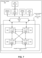
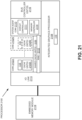
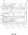
- the DPU 3504 is shown to provide processing capabilities that include a Network Interface Controller (NIC) subsystem 3508 and a processor cores subsystem 3512.
- NIC Network Interface Controller
- the NIC subsystem 3508 and processor cores subsystem 3512 are shown to be connectable through a PCIe switch 3516.
- the DPU 3504 is shown to include a NIC subsystem 3508 and processor cores subsystem 3512, it should be appreciated that the DPU 3504 can provide other processor functions or types including, without limitation, CPU processors, GPU processors, and/or any other suitable type of processing architecture.
- the processor cores subsystem 3512 may be configured to provide general processing capabilities and may include a processing complex 3520, one or more acceleration engines 3524, and one or more network interfaces 3528.
- the processing complex 3520 may include one or multiple processing cores (e.g., Advanced RISC Machine (ARM) processing cores, RISCV cores, CPU cores, GPU cores, etc.).
- ARM Advanced RISC Machine
- RISCV RISCV cores
- CPU cores CPU cores
- GPU cores etc.
- one or more processing cores of the processing complex 3520 may include programmable cores 3536 and/or approximation circuitry 3548 as shown in the NIC subsystem 3508; however, such components are not shown for ease of reference and discussion.
- the acceleration engine(s) 3524 may provide hardware acceleration capabilities for the processors in the processing complex 3520 and/or for external GPU(s) 3564.
- a processing core in the processing complex 3520 may use one or more acceleration engines 3524 to perform a specific function whereas other undefined functions may be performed within the processing core of the processing complex 3520.
- the acceleration engine(s) 3524 can be appropriately configured to perform specified functions more quickly, with fewer computations, etc. as compared to other components of the processing complex 3520.
- the network interface(s) 3528 may provide connectivity between components of the processor cores subsystem 3512 and other components external to the processor cores subsystem 3512. Illustratively, the network interface(s) 3528 may provide connectivity to the PCIe switch 3516 and/or one or more other external elements, such as an external network 3552, a DDR 3556, an SSD 3560, and/or a GPU 3564.
- the network interface(s) 3528 may include physical, mechanical, optical, and/or electrical components that allow a remote device to communicate with the processing complex 3520 and/or acceleration engine(s) 3524 of the processor cores subsystem 3512.
- the network interface(s) 3528 may enable physical connections to a cable, wire, fiberoptic, etc.
- the network interface(s) 3528 may facilitate wireless communications, in which they may include one or more antennas, drivers, or the like.
- the NIC subsystem 3508 is illustrated as another element of the DPU 3504. It should be appreciated that the components of the NIC subsystem 3508 and components of the processor cores subsystem 3512 may be in communication with one another via the PCIe switch 3516 or by some other communication mechanism.
- the NIC subsystem 3508 and processor cores subsystem 3512 may be provided on a common substrate, motherboard, or silicon. Alternatively, the NIC subsystem 3508 and processor cores subsystem 3512 may be provided on totally separate substrates, motherboards, or silicon.
- the NIC subsystem 3508 may provide functionality similar to a network adapter or other type of networking device. Illustrated components provided in the NIC subsystem 3508 include, without limitation, a Data Processing Accelerator (DPA) 3532 and one or more network interfaces 3528.
- the DPA 3532 may include one or more programmable cores 3536, memory 3540, a vector instruction list 3544, and approximation circuitry 3548. While illustrated as separate components, it should be appreciated that certain components of the DPA 3532 may be combined with one another.
- the vector instruction list 3544 and/or approximation circuitry 3548 may be included in the one or more programmable cores 3536.
- the memory 3540 may be provided external to the DAP 3532 or may be integrated as part of the programmable core(s) 3536.
- the programmable core(s) 3536 may include one or more hardware and/or software components that are programmable and may support one or more functions of the DPU 3504. Examples of a suitable programmable core 3536 include, without limitation, a programmable logic core (PLC), a programmable logic array (PLA), etc.
- the programmable core(s) 3536 may be implemented in hardware and/or software on any type of medium. For instance, the programmable core(s) 3536 may be provided as a programmable SoC, a programmable ASIC, a programmable digital circuit, combinations thereof, or the like.
- the programmable core(s) 3536 may be similar or identical to other cores described herein, such as processing cores that were described as being included in the processing complex 3520.
- the memory 3540 may correspond to any suitable type of memory device or collection of memory devices already described herein.
- Non-limiting examples of devices that may be provided as memory 3540 include RAM, ROM, flash memory, buffer memory, combinations thereof, and the like.
- the memory 3540 may be cache line aligned.
- the vector instruction list 3544 may include one or more instructions (e.g., vector instructions) that are capable of being performed in the programmable core(s) 3536.
- the vector instruction list 3544 may provide a listing of functions that can be performed by the approximation circuitry 3548 or by other components (e.g., programmable core(s) 3536, the GPU(s) 3532, etc.).
- functions e.g., vector functions
- functions that may be supported by the DPU 3504 and, thereby, made available in the vector instruction list 3544 include, without limitation, non-linear functions, linear functions, a hyperbolic tangent function (tanh(x)) function, a sigmoid function, a Rectified Linear Activation (ReLU) function, a softmax function, a softsign function, and an Exponential Linear Unit (ELU) function.
- Other suitable functions may also be listed in the vector instruction list.
- Non-limiting examples of such functions other than an activation function include a multiply add function, a vector accumulate function, a vector add function, a vector multiply function, a vector load function, and a vector store function.
- One or more of the instructions provided in the vector instruction list 3544 may be carried out completely in hardware (e.g., using the approximation circuitry 3548) and/or may utilize buffer(s) and/or a lookup table as will be described herein.
- the approximation circuitry 3548 may be configured to compute approximations of functions listed in the vector instruction list 3544 and such approximations may be computed alone or with the assistance of additional components such as a buffer and/or a lookup table.
- the network interface 3528 may be similar or identical to the network interface 3528 included in the processor cores subsystem 3512 and may include hardware and/or software components that enable operations of the NIC subsystem 3508 at the network layer.
- the network interface 3528 may also facilitate connectivity to the PCIe switch 3516. Examples of protocols that may be supported by the network interface 3528 include, without limitation, Ethernet, WiFi, Fibre Channel, Asynchronous Transfer Mode (ATM), Fiber Distributed Data Interface (FDDI), RDMA/TCP/UDP, ASAP 2 , InfiniBand, etc.
- the PCIe switch 3516 may include hardware and/or software that includes an expansion bus for a PCIe hierarchy on the DPU 3504. In some embodiments, the PCIe switch 3516 may include switching logic that routes packets between one or more ports of the PCIe switch 3516. The PCIe switch 3516 may include two or more different ports that are included as or that are connected to the network interface(s) 3528 of the NIC subsystem 3508 and processor cores subsystem 3512.
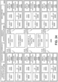
- An instruction 3600 that can be processed within the DPU 3504 may include a sign bit (S) in a sign bit field 3604, one or more exponent bits (E) in an exponent bit field 3608, and one or more mantissa bits (M) in a mantissa bit field 3612.
- the instruction 3600 may be provided in any suitable instruction format.
- Non-limiting examples of instruction formats that may be used for the instruction 3600 include float32, float16, bfloat16, etc.
- the instruction 3600 may include one sign bit field 3604, eight exponent bit fields 3608, and at least seven mantissa bit fields 3612.
- the instruction may include a greater or lesser number of exponent bit fields 3608 and/or a greater or lesser number of mantissa bit fields 3612.
- the DPU 3504 and, specifically the approximation circuitry 3548, may be configured to receive input vectors in the form of or including the instruction 3600. Said another way, the DPU 3504 may be configured to operate on instructions 3600 and/or vectors having the format depicted in FIG. 36 . Alternatively or additionally, the DPU 3504, the programmable core(s) 3536, and/or approximation circuitry 3548 may be configured to process a portion of an instruction 3600. In some embodiments, the instruction 3600 may be provided as a 16-bit vector (e.g., with a total of 16 bit fields).
- the instruction 3600 can be provided as an operation code (Opcode), or any other suitable form or format.
- the instruction 3600 or input processed by the programmable core(s) 3536 and/or approximation circuitry 3548 may include a machine language instruction or portion of machine language instruction that specifies an operation to be performed by the circuitry.
- the operation specified by the instruction includes a multiplication operation, vector activation function, non-linear function, etc.
- FIG. 37 an example of a matrix multiplication approach that may be implemented by the programmable core(s) 3536 and/or approximation circuitry 3548 in connection with performing an activation function will be described.
- machine learning inference may sometimes involve multiplying a matrix with a vector.
- the matrix holds fixed weights while the vector content is variable.
- SIMD vector single instruction, multiple data
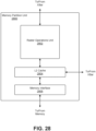
- a matrix 3704 is multiplied with vector 3712 to obtain a resultant vector 3716.
- the matrix 3704 is shown to be organized in memory by columns 3708, but it should be appreciated that the matrix 3704 can alternatively be organized by rows without departing from the scope of the present disclosure.
- the illustrative, but non-limiting, matrix 3704 of FIG. 37 is shown to include 16 rows and 32 columns, forming a 16 x 32 matrix 3704.
- the matrix 3704 is organized in memory by columns 3708. For each column 3708 the following process is followed. A scalar value is extracted from an input vector 3712. The extracted scalar value is vector multiplied with each of the elements in the corresponding/associated column 3708. For example, if the scalar value is extracted from the first element (e.g., the top-most element) of the input vector 3712, then the extracted scalar value is multiplied with each of the elements in the first column 3708 (e.g., the left-most column).
- the first element e.g., the top-most element
- the extracted scalar value is multiplied with each of the elements in the second column 3708 (e.g., the second-left-most column).
- results of the vector multiplication described above are then added together.
- the results of the vector multiplication are added element-by-element to a vector accumulator.
- the output vector 3716 is constructed with each element of the output vector 3716 having the results of each element-by-element addition.
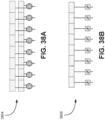
- FIGS. 38A and 38B two illustrative configurations of circuitry 3804 and 3808 that may be used as part of the approximation circuitry 3548 will be described.
- the configuration of elements depicted and described in FIGS. 38A and 38B are intended to provide examples and should not be construed as limiting the claims to any particular configuration of circuit elements.
- the circuitry 3804 of FIG. 38A is illustrated to include a number of adders.
- the circuitry 3804 may facilitate a vector add instruction with a vector size of eight elements.
- FIG. 38B illustrates circuitry 3808 that may facilitate a vector tanh function with a vector size of eight elements. It should be appreciated that either circuitry 3804, 3808 may be adjusted to accommodate larger or smaller vectors.
- the illustrated types of circuitry 3804, 3808 may be configured to obtain 16 operations per clock cycle, meaning that each clock cycle will output 16 operations. Circuitry 3804, 3808 may be expanded to support more operations per clock cycle or contracted to support fewer operations per clock cycle.
- the circuitry 3804, 3808 may be provided as part of the approximation circuitry 3548 to support performance of vector activation functions defined in the vector instruction list 3544. Because all operations can be performed on the data using the approximation circuitry 3548, it becomes possible to perform vector activation functions without requiring access to separate memory 3516, thereby increasing the speed of processing.
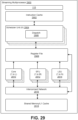
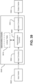
- Approximation circuitry 3548 is configured to include one or more input circuits 3904, one or more approximation circuits 3908, one or more output circuits 3912, and a lookup table 3916. While the components of the approximation circuitry 3548 are shown as being separate or distinct components, it should be appreciated that the input circuit(s) 3904, approximation circuit(s) 3908, and/or output circuit(s) 3912 may be combined into a single circuit or may be divided into more circuits than depicted.
- lookup table 3916 is shown as being included in the approximation circuitry 3548, it should be appreciated that the lookup table 3916 may be outside and separate from the approximation circuitry 3548.
- the lookup table 3916 may provide information that supports vector aggregation. Alternatively or additionally, the lookup table 3916 may correspond to a hardware-based lookup table.
- the lookup table 3916 identifies particular circuits to use within the approximation circuitry 3548 when processing a particular instruction (e.g., when approximating a specific function). As an example, the lookup table 3916 may identify first circuitry to use when approximating a first activation function and the lookup table 3916 may identify second circuitry to use when approximating a second activation function.
- the approximation circuitry 3548 receives an input vector 3920 at the input circuit(s) 3904 and then provide the input vector to the approximation circuit(s) 3908.
- the approximation circuit(s) 3908 then applies an activation function to the input vector by performing a hardware approximation of the activation function in a vector manner.
- the output circuit(s) 3912 then generates an output vector 3924 based on the activation function.
- the lookup table 3916 is referenced during the hardware approximation of the activation function. Moreover, the lookup table 3916 may be used to reference associated hardware to use during the approximation of the activation function (e.g., different hardware and/or circuitry may be used to perform the approximation of different activation functions). In some embodiments, the hardware approximation of the activation function may be performed in the absence of performing a memory 3516 lookup.
- a process such as those processes described herein is performed under control of one or more computer systems configured with executable instructions and is implemented as code (e.g., executable instructions, one or more computer programs or one or more applications) executing collectively on one or more processors, by hardware or combinations thereof.
- code is stored on a computer-readable storage medium, for example, in form of a computer program comprising a plurality of instructions executable by one or more processors.
- a computer-readable storage medium is a non-transitory computer-readable storage medium that excludes transitory signals (e.g., a propagating transient electric or electromagnetic transmission) but includes non-transitory data storage circuitry (e.g., buffers, cache, and queues) within transceivers of transitory signals.
- code e.g., executable code or source code
- code is stored on a set of one or more non-transitory computer-readable storage media having stored thereon executable instructions (or other memory to store executable instructions) that, when executed (i.e., as a result of being executed) by one or more processors of a computer system, cause computer system to perform operations described herein.
- set of non-transitory computer-readable storage media comprises multiple non-transitory computer-readable storage media and one or more of individual non-transitory storage media of multiple non-transitory computer-readable storage media lack all of code while multiple non-transitory computer-readable storage media collectively store all of code.
- executable instructions are executed such that different instructions are executed by different processors - for example, a non-transitory computer-readable storage medium store instructions and a main central processing unit (“CPU") executes some of instructions while a graphics processing unit (“GPU”) executes other instructions.
- different components of a computer system have separate processors and different processors execute different subsets of instructions.
- computer systems are configured to implement one or more services that singly or collectively perform operations of processes described herein and such computer systems are configured with applicable hardware and/or software that enable performance of operations.
- a computer system that implements at least one embodiment of present disclosure is a single device and, in another embodiment, is a distributed computer system comprising multiple devices that operate differently such that distributed computer system performs operations described herein and such that a single device does not perform all operations.
- processor or “processing unit” may refer to any device or portion of a device that processes electronic data from registers and/or memory and transform that electronic data into other electronic data that may be stored in registers and/or memory.
- processor may be a CPU or a GPU.
- a “computing platform” may comprise one or more processors or processing units.
- software processes may include, for example, software and/or hardware entities that perform work over time, such as tasks, threads, and intelligent agents. Also, each process may refer to multiple processes, for carrying out instructions in sequence or in parallel, continuously or intermittently.
- system and “method” are used herein interchangeably insofar as system may embody one or more methods and methods may be considered a system.
- references may be made to obtaining, acquiring, receiving, or inputting analog or digital data into a subsystem, computer system, or computer-implemented machine.
- process of obtaining, acquiring, receiving, or inputting analog and digital data can be accomplished in a variety of ways such as by receiving data as a parameter of a function call or a call to an application programming interface.
- processes of obtaining, acquiring, receiving, or inputting analog or digital data can be accomplished by transferring data via a serial or parallel interface.
- processes of obtaining, acquiring, receiving, or inputting analog or digital data can be accomplished by transferring data via a computer network from providing entity to acquiring entity.
- references may also be made to providing, outputting, transmitting, sending, or presenting analog or digital data.
- processes of providing, outputting, transmitting, sending, or presenting analog or digital data can be accomplished by transferring data as an input or output parameter of a function call, a parameter of an application programming interface or interprocess communication mechanism.
Landscapes
- Engineering & Computer Science (AREA)
- Physics & Mathematics (AREA)
- Theoretical Computer Science (AREA)
- Health & Medical Sciences (AREA)
- Life Sciences & Earth Sciences (AREA)
- Biomedical Technology (AREA)
- Biophysics (AREA)
- Evolutionary Computation (AREA)
- General Engineering & Computer Science (AREA)
- Data Mining & Analysis (AREA)
- Artificial Intelligence (AREA)
- General Health & Medical Sciences (AREA)
- Molecular Biology (AREA)
- Computing Systems (AREA)
- Computational Linguistics (AREA)
- General Physics & Mathematics (AREA)
- Mathematical Physics (AREA)
- Software Systems (AREA)
- Neurology (AREA)
- Image Analysis (AREA)
- Advance Control (AREA)
Claims (13)
- Verarbeitungseinheit, die dafür konfiguriert ist, Anweisungen auszuführen, umfassend:eine Schaltung (3548), die als Reaktion auf eine Anweisung einen Eingangsvektor (3904) empfängt, eine Aktivierungsfunktion auf den Eingangsvektor anwendet, indem sie eine Hardware-Approximation der Aktivierungsfunktion durchführt, und dann einen Ausgangsvektor (3924) basierend auf der Aktivierungsfunktion erzeugt; undeine Nachschlagetabelle (3916), auf die während der Hardware-Approximation der Aktivierungsfunktion Bezug genommen wird, wobei die Nachschlagetabelle bestimmte Schaltkreise der Schaltung identifiziert, die bei der Verarbeitung einer bestimmten Aktivierungsfunktion zu verwenden sind.
- Verarbeitungseinheit nach Anspruch 1, wobei die Hardware-Approximation der Aktivierungsfunktion ohne Durchführung eines Speicher- (3540) Nachschlags durchgeführt wird.
- Verarbeitungseinheit nach einem der vorhergehenden Ansprüche, wobei der Eingangsvektor Teil einer Matrix ist.
- Verarbeitungseinheit nach einem der vorhergehenden Ansprüche, wobei die Aktivierungsfunktion auf einer Vektor-Befehlsliste (3544) verfügbar gemacht wird.
- Verarbeitungseinheit nach einem der vorhergehenden Ansprüche, wobei die Aktivierungsfunktion eine Sigmoid-Funktion oder eine tanh(x)-Funktion umfasst.
- Verarbeitungseinheit eines der Ansprüche 1 bis 5, wobei die Aktivierungsfunktion eine nicht-lineare Funktion umfasst.
- Verarbeitungseinheit nach einem der vorhergehenden Ansprüche, wobei der Eingangsvektor N Elemente umfasst und wobei die Schaltung die Hardware-Approximation der Aktivierungsfunktion für jedes der N Elemente während eines einzelnen Taktzyklus durchführt.
- System, das Folgendes umfasst:
eine Verarbeitungseinheit, die dafür konfiguriert ist, Anweisungen auszuführen, umfassend:eine Schaltung (3548), die als Reaktion auf eine Anweisung einen Eingangsvektor (3904) empfängt, eine Aktivierungsfunktion auf den Eingangsvektor anwendet, indem sie eine Hardware-Approximation der Aktivierungsfunktion durchführt, und dann einen Ausgangsvektor (3924) basierend auf der Aktivierungsfunktion erzeugt; undeine Nachschlagetabelle (3916), auf die während der Hardware-Approximation der Aktivierungsfunktion Bezug genommen wird, und wobei die Nachschlagetabelle bestimmte Schaltkreise der Schaltung identifiziert, die bei der Verarbeitung einer bestimmten Aktivierungsfunktion zu verwenden sind. - System nach Anspruch 8, wobei die Verarbeitungseinheit eine Zentralverarbeitungseinheit umfasst.
- System nach Anspruch 8, wobei die Verarbeitungseinheit eine Grafikverarbeitungseinheit umfasst.
- System nach Anspruch 8, wobei die Verarbeitungseinheit eine Datenverarbeitungseinheit umfasst.
- System nach einem der Ansprüche 8 bis 11, wobei die Hardware-Approximation der Aktivierungsfunktion durchgeführt wird, ohne dass ein Speicherlese- oder Speicherschreibvorgang durchgeführt wird.
- Vorrichtung, die die Verarbeitungseinheit nach einem der Ansprüche 1 bis 7 umfasst.
Applications Claiming Priority (1)
| Application Number | Priority Date | Filing Date | Title |
|---|---|---|---|
| US17/500,598 US20230110285A1 (en) | 2021-10-13 | 2021-10-13 | Vector activation function to support machine learning inference and other processes |
Publications (2)
| Publication Number | Publication Date |
|---|---|
| EP4167141A1 EP4167141A1 (de) | 2023-04-19 |
| EP4167141B1 true EP4167141B1 (de) | 2025-01-29 |
Family
ID=83692753
Family Applications (1)
| Application Number | Title | Priority Date | Filing Date |
|---|---|---|---|
| EP22201464.9A Active EP4167141B1 (de) | 2021-10-13 | 2022-10-13 | Vektoraktivierungsfunktion zur unterstützung von maschinenlerninferenzen und anderen prozessen |
Country Status (3)
| Country | Link |
|---|---|
| US (1) | US20230110285A1 (de) |
| EP (1) | EP4167141B1 (de) |
| CN (1) | CN115983335A (de) |
Families Citing this family (5)
| Publication number | Priority date | Publication date | Assignee | Title |
|---|---|---|---|---|
| US12131599B1 (en) * | 2021-11-30 | 2024-10-29 | Zoox, Inc. | Vehicle operation and/or simulation based on decision registry |
| US20240311191A1 (en) * | 2023-03-14 | 2024-09-19 | Advanced Micro Devices, Inc. | Network-attached hostless accelerator devices |
| WO2025050067A1 (en) * | 2023-08-31 | 2025-03-06 | Strong Force Vcn Portfolio 2019, Llc | Systems, methods, kits, and apparatuses for specialized chips for robotic intelligence layers |
| CN117215969A (zh) * | 2023-09-13 | 2023-12-12 | 北京地平线信息技术有限公司 | 从存储单元中查找输入数据对应的输出数据的方法及装置 |
| WO2025170978A1 (en) * | 2024-02-05 | 2025-08-14 | Tenstorrent USA, Inc. | Multicore processors with resource sharing clusters for ai acceleration |
Family Cites Families (11)
| Publication number | Priority date | Publication date | Assignee | Title |
|---|---|---|---|---|
| US11244225B2 (en) * | 2015-07-10 | 2022-02-08 | Samsung Electronics Co., Ltd. | Neural network processor configurable using macro instructions |
| US10387366B2 (en) * | 2015-10-08 | 2019-08-20 | Via Alliance Semiconductor Co., Ltd. | Neural network unit with shared activation function units |
| CN107292382A (zh) * | 2016-03-30 | 2017-10-24 | 中国科学院声学研究所 | 一种神经网络声学模型激活函数定点量化方法 |
| GB201607713D0 (en) * | 2016-05-03 | 2016-06-15 | Imagination Tech Ltd | Convolutional neural network |
| US11977968B2 (en) * | 2017-04-20 | 2024-05-07 | Shanghai Cambricon Information Technology Co., Ltd. | Sparse processing in neural network processors |
| US10585703B2 (en) * | 2017-06-03 | 2020-03-10 | Apple Inc. | Dynamic operation allocation for neural networks |
| GB2568087B (en) * | 2017-11-03 | 2022-07-20 | Imagination Tech Ltd | Activation functions for deep neural networks |
| US11501140B2 (en) * | 2018-06-19 | 2022-11-15 | International Business Machines Corporation | Runtime reconfigurable neural network processor core |
| US11775805B2 (en) * | 2018-06-29 | 2023-10-03 | Intel Coroporation | Deep neural network architecture using piecewise linear approximation |
| US12518166B2 (en) * | 2018-12-18 | 2026-01-06 | Movidius Ltd. | Neural network compression |
| US12045724B2 (en) * | 2018-12-31 | 2024-07-23 | Microsoft Technology Licensing, Llc | Neural network activation compression with outlier block floating-point |
-
2021
- 2021-10-13 US US17/500,598 patent/US20230110285A1/en active Pending
-
2022
- 2022-09-06 CN CN202211085372.XA patent/CN115983335A/zh active Pending
- 2022-10-13 EP EP22201464.9A patent/EP4167141B1/de active Active
Non-Patent Citations (3)
| Title |
|---|
| DATABASE INSPEC [online] THE INSTITUTION OF ELECTRICAL ENGINEERS, STEVENAGE, GB; 25 April 2021 (2021-04-25), RAN WU ET AL: "Accelerating neural network inference on fpga-based platforms: a survey", Database accession no. 21211024 * |
| ELECTRONICS MDPI SWITZERLAND, vol. 10, no. 9, 25 April 2021 (2021-04-25), ISSN: 2079-9292, DOI: 10.3390/ELECTRONICS10091025 * |
| WU RAN ET AL: "Accelerating Neural Network Inference on FPGA-Based Platforms-A Survey", ELECTRONICS, vol. 10, no. 9, 25 April 2021 (2021-04-25), Basel, Switzerland, pages 1025, XP093147509, ISSN: 2079-9292, DOI: 10.3390/electronics10091025 * |
Also Published As
| Publication number | Publication date |
|---|---|
| EP4167141A1 (de) | 2023-04-19 |
| CN115983335A (zh) | 2023-04-18 |
| US20230110285A1 (en) | 2023-04-13 |
Similar Documents
| Publication | Publication Date | Title |
|---|---|---|
| CN111291880B (zh) | 计算装置以及计算方法 | |
| US12073215B2 (en) | Computing device with a conversion unit to convert data values between various sizes of fixed-point and floating-point data | |
| EP3944157A1 (de) | Vorrichtung und verfahren zur durchführung des trainings eines neuronalen faltungsnetzes | |
| KR102354722B1 (ko) | 계산 장치 및 방법 | |
| US12131250B2 (en) | Inner product convolutional neural network accelerator | |
| EP3614259A1 (de) | Verarbeitungsvorrichtung und verarbeitungsverfahren | |
| CN117642721A (zh) | 机器学习加速器中的部分和累加的调度感知、动态可重新配置加法器树体系结构 | |
| EP3451242A1 (de) | Vorrichtung und verfahren zur durchführung von reversetraining vollständig verbundener schichten eines neuronalen netzes | |
| EP2725485A2 (de) | Speicherverbindungsnetzwerkarchitektur für Vektorprozessor | |
| CN110163357A (zh) | 一种计算装置及方法 | |
| US11494326B1 (en) | Programmable computations in direct memory access engine | |
| CN111381871B (zh) | 运算方法、装置及相关产品 | |
| EP3451238A1 (de) | Vorrichtung und verfahren zur ausführung einer pooling-operation | |
| CN115310037B (zh) | 矩阵乘法计算装置、加速装置、计算系统和相关方法 | |
| CN110163350A (zh) | 一种计算装置及方法 | |
| CN116468087A (zh) | 用于执行深度神经网络的计算的硬件加速器和包括其的电子设备 | |
| EP3709225A1 (de) | System und verfahren zur effizienten nutzung von multiplikatoren in berechnungen neuronaler netzwerke | |
| CN113869517A (zh) | 一种基于深度学习模型的推理方法 | |
| WO2017177446A1 (zh) | 支持离散数据表示的人工神经网络反向训练装置和方法 | |
| US12437182B2 (en) | Neural network acceleration | |
| CN115438777A (zh) | 对神经元数据执行Winograd卷积正变换的装置 | |
| CN115081600A (zh) | 执行Winograd卷积的变换单元、集成电路装置及板卡 | |
| CN114692853B (zh) | 运算单元架构、运算单元丛集及卷积运算的执行方法 | |
| CN111966402A (zh) | 指令处理方法、装置及相关产品 | |
| WO2024258649A1 (en) | Zero-detection for logic circuit multiplication |
Legal Events
| Date | Code | Title | Description |
|---|---|---|---|
| PUAI | Public reference made under article 153(3) epc to a published international application that has entered the european phase |
Free format text: ORIGINAL CODE: 0009012 |
|
| STAA | Information on the status of an ep patent application or granted ep patent |
Free format text: STATUS: THE APPLICATION HAS BEEN PUBLISHED |
|
| AK | Designated contracting states |
Kind code of ref document: A1 Designated state(s): AL AT BE BG CH CY CZ DE DK EE ES FI FR GB GR HR HU IE IS IT LI LT LU LV MC ME MK MT NL NO PL PT RO RS SE SI SK SM TR |
|
| STAA | Information on the status of an ep patent application or granted ep patent |
Free format text: STATUS: REQUEST FOR EXAMINATION WAS MADE |
|
| 17P | Request for examination filed |
Effective date: 20231019 |
|
| RBV | Designated contracting states (corrected) |
Designated state(s): AL AT BE BG CH CY CZ DE DK EE ES FI FR GB GR HR HU IE IS IT LI LT LU LV MC ME MK MT NL NO PL PT RO RS SE SI SK SM TR |
|
| STAA | Information on the status of an ep patent application or granted ep patent |
Free format text: STATUS: EXAMINATION IS IN PROGRESS |
|
| 17Q | First examination report despatched |
Effective date: 20240412 |
|
| GRAP | Despatch of communication of intention to grant a patent |
Free format text: ORIGINAL CODE: EPIDOSNIGR1 |
|
| STAA | Information on the status of an ep patent application or granted ep patent |
Free format text: STATUS: GRANT OF PATENT IS INTENDED |
|
| RAP3 | Party data changed (applicant data changed or rights of an application transferred) |
Owner name: MELLANOX TECHNOLOGIES, LTD. |
|
| INTG | Intention to grant announced |
Effective date: 20240830 |
|
| P01 | Opt-out of the competence of the unified patent court (upc) registered |
Free format text: CASE NUMBER: APP_60003/2024 Effective date: 20241106 |
|
| GRAS | Grant fee paid |
Free format text: ORIGINAL CODE: EPIDOSNIGR3 |
|
| GRAA | (expected) grant |
Free format text: ORIGINAL CODE: 0009210 |
|
| STAA | Information on the status of an ep patent application or granted ep patent |
Free format text: STATUS: THE PATENT HAS BEEN GRANTED |
|
| AK | Designated contracting states |
Kind code of ref document: B1 Designated state(s): AL AT BE BG CH CY CZ DE DK EE ES FI FR GB GR HR HU IE IS IT LI LT LU LV MC ME MK MT NL NO PL PT RO RS SE SI SK SM TR |
|
| REG | Reference to a national code |
Ref country code: GB Ref legal event code: FG4D |
|
| REG | Reference to a national code |
Ref country code: CH Ref legal event code: EP |
|
| REG | Reference to a national code |
Ref country code: DE Ref legal event code: R096 Ref document number: 602022010042 Country of ref document: DE |
|
| REG | Reference to a national code |
Ref country code: IE Ref legal event code: FG4D |
|
| REG | Reference to a national code |
Ref country code: NL Ref legal event code: MP Effective date: 20250129 |
|
| PG25 | Lapsed in a contracting state [announced via postgrant information from national office to epo] |
Ref country code: NL Free format text: LAPSE BECAUSE OF FAILURE TO SUBMIT A TRANSLATION OF THE DESCRIPTION OR TO PAY THE FEE WITHIN THE PRESCRIBED TIME-LIMIT Effective date: 20250129 |
|
| PG25 | Lapsed in a contracting state [announced via postgrant information from national office to epo] |
Ref country code: RS Free format text: LAPSE BECAUSE OF FAILURE TO SUBMIT A TRANSLATION OF THE DESCRIPTION OR TO PAY THE FEE WITHIN THE PRESCRIBED TIME-LIMIT Effective date: 20250429 |
|
| PG25 | Lapsed in a contracting state [announced via postgrant information from national office to epo] |
Ref country code: FI Free format text: LAPSE BECAUSE OF FAILURE TO SUBMIT A TRANSLATION OF THE DESCRIPTION OR TO PAY THE FEE WITHIN THE PRESCRIBED TIME-LIMIT Effective date: 20250129 |
|
| PG25 | Lapsed in a contracting state [announced via postgrant information from national office to epo] |
Ref country code: PL Free format text: LAPSE BECAUSE OF FAILURE TO SUBMIT A TRANSLATION OF THE DESCRIPTION OR TO PAY THE FEE WITHIN THE PRESCRIBED TIME-LIMIT Effective date: 20250129 |
|
| PG25 | Lapsed in a contracting state [announced via postgrant information from national office to epo] |
Ref country code: ES Free format text: LAPSE BECAUSE OF FAILURE TO SUBMIT A TRANSLATION OF THE DESCRIPTION OR TO PAY THE FEE WITHIN THE PRESCRIBED TIME-LIMIT Effective date: 20250129 |
|
| REG | Reference to a national code |
Ref country code: LT Ref legal event code: MG9D |
|
| PG25 | Lapsed in a contracting state [announced via postgrant information from national office to epo] |
Ref country code: NO Free format text: LAPSE BECAUSE OF FAILURE TO SUBMIT A TRANSLATION OF THE DESCRIPTION OR TO PAY THE FEE WITHIN THE PRESCRIBED TIME-LIMIT Effective date: 20250429 Ref country code: IS Free format text: LAPSE BECAUSE OF FAILURE TO SUBMIT A TRANSLATION OF THE DESCRIPTION OR TO PAY THE FEE WITHIN THE PRESCRIBED TIME-LIMIT Effective date: 20250529 |
|
| REG | Reference to a national code |
Ref country code: AT Ref legal event code: MK05 Ref document number: 1764177 Country of ref document: AT Kind code of ref document: T Effective date: 20250129 |
|
| PG25 | Lapsed in a contracting state [announced via postgrant information from national office to epo] |
Ref country code: HR Free format text: LAPSE BECAUSE OF FAILURE TO SUBMIT A TRANSLATION OF THE DESCRIPTION OR TO PAY THE FEE WITHIN THE PRESCRIBED TIME-LIMIT Effective date: 20250129 |
|
| PG25 | Lapsed in a contracting state [announced via postgrant information from national office to epo] |
Ref country code: LV Free format text: LAPSE BECAUSE OF FAILURE TO SUBMIT A TRANSLATION OF THE DESCRIPTION OR TO PAY THE FEE WITHIN THE PRESCRIBED TIME-LIMIT Effective date: 20250129 Ref country code: PT Free format text: LAPSE BECAUSE OF FAILURE TO SUBMIT A TRANSLATION OF THE DESCRIPTION OR TO PAY THE FEE WITHIN THE PRESCRIBED TIME-LIMIT Effective date: 20250529 |
|
| PG25 | Lapsed in a contracting state [announced via postgrant information from national office to epo] |
Ref country code: BG Free format text: LAPSE BECAUSE OF FAILURE TO SUBMIT A TRANSLATION OF THE DESCRIPTION OR TO PAY THE FEE WITHIN THE PRESCRIBED TIME-LIMIT Effective date: 20250129 Ref country code: GR Free format text: LAPSE BECAUSE OF FAILURE TO SUBMIT A TRANSLATION OF THE DESCRIPTION OR TO PAY THE FEE WITHIN THE PRESCRIBED TIME-LIMIT Effective date: 20250430 |
|
| PG25 | Lapsed in a contracting state [announced via postgrant information from national office to epo] |
Ref country code: AT Free format text: LAPSE BECAUSE OF FAILURE TO SUBMIT A TRANSLATION OF THE DESCRIPTION OR TO PAY THE FEE WITHIN THE PRESCRIBED TIME-LIMIT Effective date: 20250129 |
|
| PG25 | Lapsed in a contracting state [announced via postgrant information from national office to epo] |
Ref country code: SE Free format text: LAPSE BECAUSE OF FAILURE TO SUBMIT A TRANSLATION OF THE DESCRIPTION OR TO PAY THE FEE WITHIN THE PRESCRIBED TIME-LIMIT Effective date: 20250129 |
|
| PG25 | Lapsed in a contracting state [announced via postgrant information from national office to epo] |
Ref country code: SM Free format text: LAPSE BECAUSE OF FAILURE TO SUBMIT A TRANSLATION OF THE DESCRIPTION OR TO PAY THE FEE WITHIN THE PRESCRIBED TIME-LIMIT Effective date: 20250129 |
|
| PG25 | Lapsed in a contracting state [announced via postgrant information from national office to epo] |
Ref country code: DK Free format text: LAPSE BECAUSE OF FAILURE TO SUBMIT A TRANSLATION OF THE DESCRIPTION OR TO PAY THE FEE WITHIN THE PRESCRIBED TIME-LIMIT Effective date: 20250129 |
|
| PG25 | Lapsed in a contracting state [announced via postgrant information from national office to epo] |
Ref country code: IT Free format text: LAPSE BECAUSE OF FAILURE TO SUBMIT A TRANSLATION OF THE DESCRIPTION OR TO PAY THE FEE WITHIN THE PRESCRIBED TIME-LIMIT Effective date: 20250129 |
|
| PGFP | Annual fee paid to national office [announced via postgrant information from national office to epo] |
Ref country code: FR Payment date: 20250924 Year of fee payment: 4 |
|
| PG25 | Lapsed in a contracting state [announced via postgrant information from national office to epo] |
Ref country code: EE Free format text: LAPSE BECAUSE OF FAILURE TO SUBMIT A TRANSLATION OF THE DESCRIPTION OR TO PAY THE FEE WITHIN THE PRESCRIBED TIME-LIMIT Effective date: 20250129 Ref country code: CZ Free format text: LAPSE BECAUSE OF FAILURE TO SUBMIT A TRANSLATION OF THE DESCRIPTION OR TO PAY THE FEE WITHIN THE PRESCRIBED TIME-LIMIT Effective date: 20250129 |
|
| PG25 | Lapsed in a contracting state [announced via postgrant information from national office to epo] |
Ref country code: RO Free format text: LAPSE BECAUSE OF FAILURE TO SUBMIT A TRANSLATION OF THE DESCRIPTION OR TO PAY THE FEE WITHIN THE PRESCRIBED TIME-LIMIT Effective date: 20250129 |
|
| PG25 | Lapsed in a contracting state [announced via postgrant information from national office to epo] |
Ref country code: SK Free format text: LAPSE BECAUSE OF FAILURE TO SUBMIT A TRANSLATION OF THE DESCRIPTION OR TO PAY THE FEE WITHIN THE PRESCRIBED TIME-LIMIT Effective date: 20250129 |
|
| REG | Reference to a national code |
Ref country code: DE Ref legal event code: R097 Ref document number: 602022010042 Country of ref document: DE |
|
| PLBE | No opposition filed within time limit |
Free format text: ORIGINAL CODE: 0009261 |
|
| STAA | Information on the status of an ep patent application or granted ep patent |
Free format text: STATUS: NO OPPOSITION FILED WITHIN TIME LIMIT |
|
| 26N | No opposition filed |
Effective date: 20251030 |
|
| PGFP | Annual fee paid to national office [announced via postgrant information from national office to epo] |
Ref country code: DE Payment date: 20250923 Year of fee payment: 4 |