EP4166979A1 - Optical detection circuit and distance measurement device - Google Patents
Optical detection circuit and distance measurement device Download PDFInfo
- Publication number
- EP4166979A1 EP4166979A1 EP21822413.7A EP21822413A EP4166979A1 EP 4166979 A1 EP4166979 A1 EP 4166979A1 EP 21822413 A EP21822413 A EP 21822413A EP 4166979 A1 EP4166979 A1 EP 4166979A1
- Authority
- EP
- European Patent Office
- Prior art keywords
- circuit
- voltage
- photodetection
- input amplifier
- reference voltage
- Prior art date
- Legal status (The legal status is an assumption and is not a legal conclusion. Google has not performed a legal analysis and makes no representation as to the accuracy of the status listed.)
- Granted
Links
Images






Classifications
-
- G—PHYSICS
- G01—MEASURING; TESTING
- G01J—MEASUREMENT OF INTENSITY, VELOCITY, SPECTRAL CONTENT, POLARISATION, PHASE OR PULSE CHARACTERISTICS OF INFRARED, VISIBLE OR ULTRAVIOLET LIGHT; COLORIMETRY; RADIATION PYROMETRY
- G01J1/00—Photometry, e.g. photographic exposure meter
- G01J1/02—Details
- G01J1/0228—Control of working procedures; Failure detection; Spectral bandwidth calculation
-
- G—PHYSICS
- G01—MEASURING; TESTING
- G01S—RADIO DIRECTION-FINDING; RADIO NAVIGATION; DETERMINING DISTANCE OR VELOCITY BY USE OF RADIO WAVES; LOCATING OR PRESENCE-DETECTING BY USE OF THE REFLECTION OR RERADIATION OF RADIO WAVES; ANALOGOUS ARRANGEMENTS USING OTHER WAVES
- G01S7/00—Details of systems according to groups G01S13/00, G01S15/00, G01S17/00
- G01S7/48—Details of systems according to groups G01S13/00, G01S15/00, G01S17/00 of systems according to group G01S17/00
- G01S7/483—Details of pulse systems
- G01S7/486—Receivers
- G01S7/4861—Circuits for detection, sampling, integration or read-out
-
- G—PHYSICS
- G01—MEASURING; TESTING
- G01C—MEASURING DISTANCES, LEVELS OR BEARINGS; SURVEYING; NAVIGATION; GYROSCOPIC INSTRUMENTS; PHOTOGRAMMETRY OR VIDEOGRAMMETRY
- G01C3/00—Measuring distances in line of sight; Optical rangefinders
- G01C3/02—Details
- G01C3/06—Use of electric means to obtain final indication
- G01C3/08—Use of electric radiation detectors
-
- G—PHYSICS
- G01—MEASURING; TESTING
- G01J—MEASUREMENT OF INTENSITY, VELOCITY, SPECTRAL CONTENT, POLARISATION, PHASE OR PULSE CHARACTERISTICS OF INFRARED, VISIBLE OR ULTRAVIOLET LIGHT; COLORIMETRY; RADIATION PYROMETRY
- G01J1/00—Photometry, e.g. photographic exposure meter
- G01J1/42—Photometry, e.g. photographic exposure meter using electric radiation detectors
- G01J1/44—Electric circuits
-
- G—PHYSICS
- G01—MEASURING; TESTING
- G01S—RADIO DIRECTION-FINDING; RADIO NAVIGATION; DETERMINING DISTANCE OR VELOCITY BY USE OF RADIO WAVES; LOCATING OR PRESENCE-DETECTING BY USE OF THE REFLECTION OR RERADIATION OF RADIO WAVES; ANALOGOUS ARRANGEMENTS USING OTHER WAVES
- G01S17/00—Systems using the reflection or reradiation of electromagnetic waves other than radio waves, e.g. lidar systems
- G01S17/88—Lidar systems specially adapted for specific applications
- G01S17/89—Lidar systems specially adapted for specific applications for mapping or imaging
- G01S17/894—Three-dimensional [3D] imaging with simultaneous measurement of time-of-flight at a two-dimensional [2D] array of receiver pixels, e.g. time-of-flight cameras or flash lidar
-
- G—PHYSICS
- G01—MEASURING; TESTING
- G01S—RADIO DIRECTION-FINDING; RADIO NAVIGATION; DETERMINING DISTANCE OR VELOCITY BY USE OF RADIO WAVES; LOCATING OR PRESENCE-DETECTING BY USE OF THE REFLECTION OR RERADIATION OF RADIO WAVES; ANALOGOUS ARRANGEMENTS USING OTHER WAVES
- G01S7/00—Details of systems according to groups G01S13/00, G01S15/00, G01S17/00
- G01S7/48—Details of systems according to groups G01S13/00, G01S15/00, G01S17/00 of systems according to group G01S17/00
- G01S7/483—Details of pulse systems
- G01S7/486—Receivers
- G01S7/4861—Circuits for detection, sampling, integration or read-out
- G01S7/4863—Detector arrays, e.g. charge-transfer gates
-
- G—PHYSICS
- G01—MEASURING; TESTING
- G01S—RADIO DIRECTION-FINDING; RADIO NAVIGATION; DETERMINING DISTANCE OR VELOCITY BY USE OF RADIO WAVES; LOCATING OR PRESENCE-DETECTING BY USE OF THE REFLECTION OR RERADIATION OF RADIO WAVES; ANALOGOUS ARRANGEMENTS USING OTHER WAVES
- G01S7/00—Details of systems according to groups G01S13/00, G01S15/00, G01S17/00
- G01S7/48—Details of systems according to groups G01S13/00, G01S15/00, G01S17/00 of systems according to group G01S17/00
- G01S7/483—Details of pulse systems
- G01S7/486—Receivers
- G01S7/487—Extracting wanted echo signals, e.g. pulse detection
- G01S7/4873—Extracting wanted echo signals, e.g. pulse detection by deriving and controlling a threshold value
-
- G—PHYSICS
- G04—HOROLOGY
- G04F—TIME-INTERVAL MEASURING
- G04F10/00—Apparatus for measuring unknown time intervals by electric means
- G04F10/005—Time-to-digital converters [TDC]
-
- H—ELECTRICITY
- H10—SEMICONDUCTOR DEVICES; ELECTRIC SOLID-STATE DEVICES NOT OTHERWISE PROVIDED FOR
- H10F—INORGANIC SEMICONDUCTOR DEVICES SENSITIVE TO INFRARED RADIATION, LIGHT, ELECTROMAGNETIC RADIATION OF SHORTER WAVELENGTH OR CORPUSCULAR RADIATION
- H10F30/00—Individual radiation-sensitive semiconductor devices in which radiation controls the flow of current through the devices, e.g. photodetectors
- H10F30/20—Individual radiation-sensitive semiconductor devices in which radiation controls the flow of current through the devices, e.g. photodetectors the devices having potential barriers, e.g. phototransistors
- H10F30/21—Individual radiation-sensitive semiconductor devices in which radiation controls the flow of current through the devices, e.g. photodetectors the devices having potential barriers, e.g. phototransistors the devices being sensitive to infrared, visible or ultraviolet radiation
- H10F30/22—Individual radiation-sensitive semiconductor devices in which radiation controls the flow of current through the devices, e.g. photodetectors the devices having potential barriers, e.g. phototransistors the devices being sensitive to infrared, visible or ultraviolet radiation the devices having only one potential barrier, e.g. photodiodes
- H10F30/225—Individual radiation-sensitive semiconductor devices in which radiation controls the flow of current through the devices, e.g. photodetectors the devices having potential barriers, e.g. phototransistors the devices being sensitive to infrared, visible or ultraviolet radiation the devices having only one potential barrier, e.g. photodiodes the potential barrier working in avalanche mode, e.g. avalanche photodiodes
-
- H—ELECTRICITY
- H10—SEMICONDUCTOR DEVICES; ELECTRIC SOLID-STATE DEVICES NOT OTHERWISE PROVIDED FOR
- H10F—INORGANIC SEMICONDUCTOR DEVICES SENSITIVE TO INFRARED RADIATION, LIGHT, ELECTROMAGNETIC RADIATION OF SHORTER WAVELENGTH OR CORPUSCULAR RADIATION
- H10F77/00—Constructional details of devices covered by this subclass
- H10F77/95—Circuit arrangements
- H10F77/953—Circuit arrangements for devices having potential barriers
- H10F77/959—Circuit arrangements for devices having potential barriers for devices working in avalanche mode
-
- G—PHYSICS
- G01—MEASURING; TESTING
- G01J—MEASUREMENT OF INTENSITY, VELOCITY, SPECTRAL CONTENT, POLARISATION, PHASE OR PULSE CHARACTERISTICS OF INFRARED, VISIBLE OR ULTRAVIOLET LIGHT; COLORIMETRY; RADIATION PYROMETRY
- G01J1/00—Photometry, e.g. photographic exposure meter
- G01J1/42—Photometry, e.g. photographic exposure meter using electric radiation detectors
- G01J1/44—Electric circuits
- G01J2001/4446—Type of detector
- G01J2001/446—Photodiode
- G01J2001/4466—Avalanche
-
- G—PHYSICS
- G01—MEASURING; TESTING
- G01S—RADIO DIRECTION-FINDING; RADIO NAVIGATION; DETERMINING DISTANCE OR VELOCITY BY USE OF RADIO WAVES; LOCATING OR PRESENCE-DETECTING BY USE OF THE REFLECTION OR RERADIATION OF RADIO WAVES; ANALOGOUS ARRANGEMENTS USING OTHER WAVES
- G01S17/00—Systems using the reflection or reradiation of electromagnetic waves other than radio waves, e.g. lidar systems
- G01S17/02—Systems using the reflection of electromagnetic waves other than radio waves
- G01S17/06—Systems determining position data of a target
- G01S17/08—Systems determining position data of a target for measuring distance only
-
- G—PHYSICS
- G01—MEASURING; TESTING
- G01S—RADIO DIRECTION-FINDING; RADIO NAVIGATION; DETERMINING DISTANCE OR VELOCITY BY USE OF RADIO WAVES; LOCATING OR PRESENCE-DETECTING BY USE OF THE REFLECTION OR RERADIATION OF RADIO WAVES; ANALOGOUS ARRANGEMENTS USING OTHER WAVES
- G01S17/00—Systems using the reflection or reradiation of electromagnetic waves other than radio waves, e.g. lidar systems
- G01S17/88—Lidar systems specially adapted for specific applications
- G01S17/93—Lidar systems specially adapted for specific applications for anti-collision purposes
- G01S17/931—Lidar systems specially adapted for specific applications for anti-collision purposes of land vehicles
Definitions
- the present disclosure relates to a photodetection circuit and a distance measuring device.
- a time of flight (ToF) method is used as a method of measuring the distance to a subject.
- ToF method reflected light obtained by light emitted from a light source being reflected by a subject is detected. Subsequently, the distance to the subject is measured on the basis of the time from the emission of the light to the detection of the reflected light.
- a distance measuring device using the ToF method is generally provided with a photodetection circuit that detects the reflected light described above.
- a photodetection circuit that detects the reflected light described above.
- a voltage change of a photodetection element obtained when photons are incident is detected.
- a reference voltage for detecting this voltage change is generally fixed.
- Patent Document 1 Japanese Patent Application Laid-Open No. 2014-81254
- the reference voltage described above is low, a distance measurement error increases due to characteristic variation of the photodetection element in some cases. In order to reduce this distance measurement error, it is desirable that the reference voltage be high.
- the dead time which is a period during which photons cannot be detected, becomes long, and the distance measurement accuracy deteriorates in some cases.
- the present disclosure provides a photodetection circuit and a distance measuring device capable of improving distance measuring performance.
- a photodetection circuit includes: an avalanche photodiode; a charging circuit that supplies a voltage to the avalanche photodiode; an input amplifier including a comparison circuit in which a voltage level of an output terminal changes according to a comparison result between a voltage of an input terminal connected to the avalanche photodiode and a reference voltage, and a voltage control circuit that changes a potential of the reference voltage; and a state detecting circuit that sets timing for causing the voltage control circuit to change the potential of the reference voltage on the basis of a detection result of the voltage level.
- the comparison circuit may include an inverter circuit
- the voltage control circuit may include a switching element that is connected to the inverter circuit and performs switching according to an output voltage of the state detecting circuit, and a resistive element or a current source that is connected in parallel with the switching element.
- the comparison circuit may include an operational amplifier circuit
- the voltage control circuit may include a switch circuit that switches the reference voltage to a first reference voltage or a second reference voltage different from the first reference voltage according to an output voltage of the state detecting circuit.
- the comparison circuit may include an inverter circuit
- the voltage control circuit may include a current source that is connected to the inverter circuit and whose output current value changes according to an output voltage of the state detecting circuit.
- the state detecting circuit may include inverter elements of odd-numbered stages connected in series with one another.
- the input amplifier may include a first input amplifier that outputs the comparison result to a signal processing circuit, and a second input amplifier that outputs the comparison result to the state detecting circuit.
- circuit configuration of the first input amplifier may be the same as circuit configuration of the second input amplifier.
- circuit configuration of the first input amplifier may be different from circuit configuration of the second input amplifier.
- the avalanche photodiode, the charging circuit, the input amplifier, and the state detecting circuit may be provided on one semiconductor substrate.
- the avalanche photodiode may be provided on a first semiconductor substrate, and the charging circuit, the input amplifier, and the state detecting circuit may be provided on a second semiconductor substrate bonded to the first semiconductor substrate.
- a quench circuit that is connected to the avalanche photodiode and the input terminal of the input amplifier and controls a potential of the input terminal may be further included.
- a cathode of the avalanche photodiode may be connected to the input terminal of the input amplifier.
- an anode of the avalanche photodiode may be connected to the input terminal of the input amplifier.
- a distance measuring device includes any one of the above-described photodetection circuits and a signal processing circuit that processes an output signal of the photodetection circuit.
- the signal processing circuit may include:
- FIG. 1 is a block diagram depicting a configuration example of an imaging system using a photodetection circuit and a distance measuring device according to a first embodiment.
- An imaging system 101 depicted in Fig. 1 is a system that captures a distance image using the ToF method, and includes an illumination device 111 and an imaging device 112.
- the illumination device 111 includes an illumination control section 121 and a light source 122.
- the illumination control section 121 controls a pattern in which the light source 122 emits irradiation light on the basis of control of the control section 132 of the imaging device 112. Specifically, the illumination control section 121 controls the pattern in which the light source 122 emits irradiation light according to the irradiation code included in the irradiation signal supplied from the control section 132.
- the irradiation code includes two values of "1" (High) and "0" (Low).
- the illumination control section 121 turns on the light source 122 when the value of the irradiation code is "1", and turns off the light source 122 when the value of the irradiation code is "0".
- the light source 122 emits light (irradiation light) in a predetermined wavelength range on the basis of control of the illumination control section 121.
- the light source 122 is, for example, an infrared laser diode.
- the type of the light source 122 and the wavelength range of the irradiation light can be arbitrarily set according to the application of the imaging system 101 or the like.
- the imaging device 112 receives reflected light obtained by irradiation light being reflected by a subject 102 and a subject 103.
- the imaging device 112 includes a distance measuring device 131, the control section 132, a display section 133, and a storage section 134.
- the distance measuring device 131 includes a lens 141, a photodetection circuit 142, and a signal processing circuit 143.
- the lens 141 forms an image of the incident light on the photodetection circuit 142.
- the lens 141 has any configuration, and for example, the lens 141 can include a plurality of lens groups.
- the photodetection circuit 142 images the subject 102, the subject 103, and the like on the basis of control of the control section 132. Furthermore, the photodetection circuit 142 outputs a signal obtained by imaging to the signal processing circuit 143.
- the signal processing circuit 143 processes the output signal of the photodetection circuit 142 on the basis of control of the control section 132. For example, the signal processing circuit 143 detects the distance to the subject on the basis of the output signal of the photodetection circuit 142 and creates a distance image indicating the distance to the subject.
- the control section 132 includes, for example, a control circuit such as a field programmable gate array (FPGA) or a digital signal processor (DSP), a processor, or the like.
- the control section 132 controls the illumination control section 121, the photodetection circuit 142, and the signal processing circuit 143.
- the display section 133 includes, for example, a panel type display device such as a liquid crystal display device or an organic electro luminescence (EL) display device.
- a panel type display device such as a liquid crystal display device or an organic electro luminescence (EL) display device.
- the storage section 134 can include any storage device, storage medium, or the like, and stores a distance image or the like.
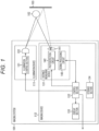
- Fig. 2 is a block diagram depicting a configuration example of the photodetection circuit 142 and the signal processing circuit 143.
- the photodetection circuit 142 includes a photodetection element 151, a charging circuit 152, a quench circuit 153, an input amplifier 154, and a state detecting circuit 155. These are provided on one semiconductor substrate.
- the photodetection circuit 142 depicted in Fig. 2 is a unit circuit corresponding to one pixel, the distance measuring device 131 includes a plurality of photodetection circuits 142 according to the number of pixels.
- the photodetection element 151 is a photodiode a typical example of which is an avalanche photo diode (APD), a single photon avalanche diode (SPAD), or the like.
- the cathode of the photodetection element 151 is connected to the charging circuit 152 and an input terminal of the input amplifier 154.
- the anode of the photodetection element 151 is set to a negative voltage VRL by a negative power supply (not illustrated).
- the charging circuit 152 includes, for example, a current source and a resistive element connected in series with each other.
- the charging circuit 152 supplies a positive voltage to the cathode of the photodetection element 151.
- a reverse voltage equal to or higher than the breakdown voltage is applied between the anode and the cathode of the photodetection element 151, the photodetection element 151 is set to the Geiger mode. If photons are incident on the photodetection element 151 set to the Geiger mode, avalanche multiplication occurs, and a current flows through the photodetection element 151.
- the quench circuit 153 includes, for example, an N-channel MOS transistor 156.
- the drain of the N-channel MOS transistor 156 is connected to the cathode of the photodetection element 151 and the input terminal of the input amplifier 154, and the source is grounded. If an external signal APDEN is input to the gate of the N-channel MOS transistor 156, a cathode voltage Vc is forcibly set to the ground potential. In this case, the photodetection function of the photodetection element 151 is deteriorated. Therefore, it is possible to avoid erroneous detection of an after-pulse in which avalanche multiplication occurs again even though no photon is incident on the photodetection element 151, or the like.
- the quench circuit 153 is not limited to the N-channel MOS transistor 156 as long as the cathode voltage Vc can be forcibly set to a potential that lowers the photodetection function of the photodetection element 151.
- the source of the N-channel MOS transistor 156 may be connected to a negative potential instead of being grounded.
- the rise of the recharge (recovery) of the cathode voltage Vc becomes slower and the dead time becomes longer.
- the dead time can be shortened by optimizing the reference voltage of the input amplifier 154.
- the input amplifier 154 compares the voltage of the input terminal, in other words, the cathode voltage Vc of the photodetection element 151, with a variable reference voltage. Furthermore, in the input amplifier 154, the voltage level of the output terminal changes according to the comparison result.
- the circuit configuration of the input amplifier 154 will be described later.
- the state detecting circuit 155 detects the voltage level of the output terminal of the input amplifier 154 and sets the timing to change the potential of the reference voltage described above. The configuration of the state detecting circuit 155 will also be described later.
- the signal processing circuit 143 includes a time to digital converter (TDC) 200, a histogram creating section 201, and a distance determining section 202.
- the time to digital converter (TDC) 200 converts an output signal of the input amplifier 154 into a digital value. Specifically, the TDC 200 digitally converts the occurrence time of the transition timing of the voltage level of the output terminal of the input amplifier 154.
- the histogram creating section 201 counts the number of times the digital value described above is acquired, that is, the number of times the photodetection element 151 reacts.
- the distance determining section 202 determines the distance from the photodetection element 151 to the subject 102, 103 on the basis of the count result of the histogram creating section 201. For example, the distance determining section 202 calculates an approximate curve for a normal distribution indicating the count result of the histogram creating section 201 (so-called Gaussian fitting), and obtains the distance by using the approximate curve.
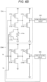
- Fig. 3A is a circuit diagram depicting configuration of the input amplifier according to the present embodiment.
- the input amplifier 154 according to the present embodiment includes an inverter circuit 161 and a voltage control circuit 162 connected to the inverter circuit 161.
- the inverter circuit 161 corresponds to a comparison circuit.
- the inverter circuit 161 includes MOS transistors 170 to 173.
- the MOS transistor 170 and the MOS transistor 172 are P-channel MOS transistors, and the MOS transistor 171 and the MOS transistor 173 are N-channel MOS transistors.
- the MOS transistor 170 and the MOS transistor 171 are connected in series. Furthermore, the MOS transistor 172 and the MOS transistor 173 are connected in series.
- Each of the gates of the MOS transistor 170 and the MOS transistor 171 is an input terminal of the input amplifier 154.
- the cathode voltage Vc of the photodetection element 151 is input to each of the gates.
- the source of the MOS transistor 170 is connected to a positive power supply, and the source of the MOS transistor 171 is connected to the voltage control circuit 162.
- Each of the drains of the MOS transistor 170 and the MOS transistor 171 is connected to each of the gates of the MOS transistor 172 and the MOS transistor 173.
- the source of the MOS transistor 172 is connected to a positive power supply, and the source of the MOS transistor 171 is grounded.
- Each of the drains of the MOS transistor 172 and the MOS transistor 173 is an output terminal of the input amplifier 154, and is connected to the state detecting circuit 155 and the signal processing circuit 143.
- the voltage control circuit 162 includes a switching element 174 and a resistive element 175.
- the switching element 174 is, for example, an N-channel MOS transistor.
- An output voltage Vo of the state detecting circuit 155 is input to the gate of the switching element 174.
- the drain is connected to the source of the MOS transistor 171.
- the source is grounded.
- the resistive element 175 is connected in parallel to the switching element 174.
- one of the MOS transistor 170 or the MOS transistor 171 is turned on and the other is turned off according to the potential of the cathode voltage Vc of the photodetection element 151. If the MOS transistor 170 is turned on, the MOS transistor 173 is turned on, and the MOS transistor 172 is turned off. In this case, a voltage level Vs becomes a low level. If the MOS transistor 171 is turned on, the MOS transistor 172 is turned on, and the MOS transistor 173 is turned off. In this case, the voltage level Vs becomes a high level.
- the threshold voltage for switching the voltage level Vs to the high level or the low level corresponds to the potential of the reference voltage.
- the potential of the reference voltage is changed by the voltage control circuit 162. If the switching element 174 of the voltage control circuit 162 is turned on, the potential of the reference voltage decreases. Conversely, if the switching element 174 is turned off, the potential of the reference voltage increases.
- Fig. 3B is a circuit diagram depicting configuration of a first modification of the input amplifier 154. Components similar to those of the input amplifier 154 illustrated in Fig. 3A are denoted by the same reference numerals, and a detailed description thereof will be omitted.
- An input amplifier 154 illustrated in Fig. 3B is different from the input amplifier 154 illustrated in Fig. 3A in the configuration of the voltage control circuit.
- a current source 175a is provided instead of the resistive element 175.
- the current source 175a is an N-channel MOS transistor.
- the drain of the N-channel MOS transistor is connected to the drain of the switching element 174, and the source is grounded.
- a reference voltage is input to the gate. This reference voltage is set such that the on-resistance of the switching element 174 is lower than the on-resistance of the current source 175a.
- Fig. 4 is a circuit diagram depicting configuration of a second modification of the input amplifier 154.
- An input amplifier 154a according to the present modification includes an inverter circuit 161a and a voltage control circuit 163 connected to the inverter circuit 161a.
- the inverter circuit 161a includes MOS transistors 170a to 173a, and thus a detailed description thereof will be omitted.
- the voltage control circuit 163 includes a current source 176a, a switch 176b, a switch 176c, and an inverter element 176d.
- the current source 176a is an N-channel MOS transistor.
- the switch 176b and the switch 176c are connected in parallel with each other to the gate of the N-channel MOS transistor.
- the drain is connected to the source of the MOS transistor 171a.
- the source is grounded.
- the output current value of the current source 176a changes according to the gate voltage of the N-channel MOS transistor. If the gate voltage decreases, the output current value decreases, and therefore, the reference voltage for switching the voltage level Vs of the inverter circuit 161a increases.
- the switch 176b and the switch 176c are turned on or off on the basis of the output voltage Vo of the state detecting circuit 155. A voltage obtained by inverting the potential of the output voltage Vo by the inverter element 176d is input to the switch 176c. Therefore, if one of the switch 176b or the switch 176c is turned on, the other is turned off. If the switch 176b is turned on, a first reference voltage Vref1 is supplied to the current source 176a as the gate voltage described above.
- the switch 176c Conversely, if the switch 176c is turned on, a second reference voltage Vref2 having a potential different from that of the first reference voltage Vref1 is supplied to the current source 176a as the gate voltage described above.
- the inverter element 176d may be provided on the switch 176b side instead of the switch 176c side.
- Fig. 5 is a circuit diagram depicting configuration of a third modification of the input amplifier 154.
- An input amplifier 154b according to the present modification includes an operational amplifier circuit 164 and a switch circuit 165.
- the operational amplifier circuit 164 is an example of the comparison circuit and includes MOS transistors 177 to 180 and a current source 181.
- the MOS transistor 177 and the MOS transistor 178 are P-channel MOS transistors and constitute a current mirror circuit.
- the MOS transistor 179 and the MOS transistor 180 are N-channel MOS transistors having the same size and the same electrical characteristics, and are connected in parallel with each other via the current mirror circuit described above.
- the gate of the MOS transistor 179 is an input terminal of the input amplifier 154b.
- the drains of the MOS transistor 178 and the MOS transistor 180 are output terminals of the input amplifier 154b.
- the current source 181 is connected to each of the sources of the MOS transistor 179 and the MOS transistor 180.
- the switch circuit 165 is a modification of the voltage control circuit 162, and includes a switch 182, a switch 183, and an inverter element 184.
- the switch 182 and the switch 183 are turned on or off on the basis of the output voltage Vo of the state detecting circuit 155.
- a voltage obtained by inverting the potential of the output voltage Vo by the inverter element 184 is input to the switch 183. Therefore, if one of the switch 182 or the switch 183 is turned on, the other is turned off. If the switch 182 is turned on, the first reference voltage Vref1 is input to the gate of the MOS transistor 180.
- the switch 183 Conversely, if the switch 183 is turned on, the second reference voltage Vref2 having a potential different from that of the first reference voltage Vref1 is input to the gate of the MOS transistor 180.
- the inverter element 184 may be provided on the switch 182 side instead of the switch 183 side.
- Fig. 6A is a circuit diagram depicting configuration of a fourth modification of the input amplifier 154.
- the present modification includes a first input amplifier 154c and a second input amplifier 154d.
- the first input amplifier 154c includes MOS transistors 170c to 173c, a switching element 174c, and a resistive element 175c.
- the gate of the MOS transistor 170c is an input terminal
- each of the drains of the MOS transistor 172c and the MOS transistor 173c is an output terminal. This output terminal is connected to the signal processing circuit 143.
- the second input amplifier 154d also includes MOS transistors 170d to 173d, a switching element 174d, and a resistive element 175d.
- the gate of the MOS transistor 170d is an input terminal
- each of the drains of the MOS transistor 172d and the MOS transistor 173d is an output terminal. This output terminal is connected to the state detecting circuit 155.
- the circuit configuration of the first input amplifier 154c is the same as the circuit configuration of the second input amplifier 154d, but may be different.
- Fig. 6B is a circuit diagram depicting configuration of a fifth modification of the input amplifier 154. Components similar to those in Fig. 6A are denoted by the same reference numerals, and a detailed description thereof will be omitted.
- configuration of the second input amplifier 154d is different from that of Fig. 6A .
- the second input amplifier 154d according to the present modification is not provided with the switching element 174d and the resistive element 175d, and the source of the MOS transistor 171d is grounded. That is, the second input amplifier 154d does not perform reference voltage control based on the output voltage Vo of the state detecting circuit 155. According to the present modification, since the cathode voltage Vc input during operation of the state detecting circuit 155 becomes constant, control is stabilized.
- Fig. 7 is a circuit diagram depicting configuration of the state detecting circuit 155.
- the state detecting circuit 155 depicted in Fig. 7 can be applied to the input amplifier 154 depicted in Figs. 3A and 3B , the input amplifier 154b depicted in Fig. 5 , and the second input amplifier 154d depicted in Figs. 6A and 6B .
- This state detecting circuit 155 includes five stages of inverter elements 190 connected in series with one another.
- the state detecting circuit 155 described above outputs an input signal after a predetermined time has elapsed.
- the predetermined time corresponds to a delay time between the input signal and the output signal.
- This delay time can be set on the basis of the number of stages of the inverter elements 190. Therefore, the number of stages of the inverter elements 190 is not limited to five, and it is sufficient if the number is an odd number. By adjusting the number of stages of the inverter elements 190, the timing of changing the reference voltage of each input amplifier can be set.
- Fig. 8 is a graph depicting an example of voltage characteristics of a plurality of photodetection elements 151.
- the horizontal axis represents time
- the vertical axis represents the cathode voltage Vc of the photodetection element.
- the drop characteristic of the cathode voltage Vc obtained when photons are incident on the photodetection element 151 is different between the photodetection elements in some cases due to variations in on-resistance and parasitic capacitance. In this case, as depicted in Fig.
- the timing of detecting the drop of the cathode voltage Vc varies, which can be a factor of a distance measurement error. In order to reduce this distance measurement error, it is desirable to set the reference voltage Vref to a high value.
- Fig. 9 is a graph depicting an example of voltage characteristics of a single photodetection element 151. Also in the graph illustrated in Fig. 9 , the horizontal axis represents time, and the vertical axis represents the cathode voltage Vc of the photodetection element 151. If photons are incident on the photodetection element 151, avalanche multiplication occurs, and a current flows through the photodetection element 151. As a result, the cathode voltage Vc drops. If the avalanche multiplication converges, the cathode voltage Vc gradually recovers.
- a dead time Tdead which is a period from when the cathode voltage Vc drops to when the cathode voltage Vc recovers, photons cannot be detected. Therefore, if the reference voltage Vref is fixed to a high value, the dead time Tdead becomes long, and the distance measuring performance can be insufficient. Therefore, in order to shorten the dead time Tdead, it is desirable to set the reference voltage Vref to a low value.
- Fig. 10 is a graph depicting voltage characteristics of the photodetection element 151 and reference voltage characteristics of the input amplifier 154. Also in the graph illustrated in Fig. 10 , the horizontal axis represents time, and the vertical axis represents the cathode voltage Vc of the photodetection element 151.
- the voltage control circuit 162 can set two reference voltages. Furthermore, the state detecting circuit 155 can set a timing to switch between the two reference voltages. Therefore, as illustrated in Fig. 10 , drop of the cathode voltage Vc can be detected at the first reference voltage Vref1 having a high potential, and recovery of the cathode voltage Vc can be detected at the second reference voltage Vref2 having a low potential.
- the timing at which the state detecting circuit 155 switches from the first reference voltage Vref1 to the second reference voltage Vref2 is matched with the timing from fall to rise of the cathode voltage Vc. Therefore, it is possible to more accurately measure drop and recovery of the cathode voltage Vc.
- the reference voltage for detecting drop of the cathode voltage Vc of the photodetection element 151 can be set high, it is possible to reduce a distance measurement error due to variation in output timing among the plurality of photodetection elements 151. Furthermore, since the reference voltage for detecting recovery of the cathode voltage Vc can be set low, the dead time can be shortened. Therefore, since the two conflicting requirements of early detection of drop and recovery of the cathode voltage Vc can be satisfied, it is possible to improve the distance measuring performance.
- Fig. 11 is a perspective view depicting a structure of a distance measuring device according to a modification. Incidentally, components similar to those of the distance measuring device 131 according to the first embodiment described above are denoted by the same reference numerals, and detailed description thereof will be omitted.
- a distance measuring device 131a depicted in Fig. 11 includes a first semiconductor substrate 301 and a second semiconductor substrate 302.
- the first semiconductor substrate 301 and the second semiconductor substrate 302 are bonded by, for example, a copper pad and are electrically connected.
- a pixel array is formed by two-dimensionally arranging the plurality of photodetection elements 151.
- the surface on which the photodetection elements 151 are formed becomes a light receiving surface S of the distance measuring device 131a.
- the second semiconductor substrate 302 has a region 312 facing the first semiconductor substrate 301 and a region 322 adjacent to the region 312.
- peripheral components of the photodetection element 151 in the photodetection circuit 142 that is, the charging circuit 152, the quench circuit 153, the input amplifier 154, and the state detecting circuit 155 are formed.
- the signal processing circuit 143 is formed in the region 322.
- the reference voltage for detecting drop of the cathode voltage Vc of the photodetection element 151 and the reference voltage for detecting recovery of the cathode voltage Vc can be separately set. Therefore, the distance measuring performance can be improved.
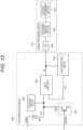
- Fig. 12 is a block diagram depicting a configuration example of a distance measuring device according to a second embodiment. Components similar to those of the distance measuring device 131 according to the first embodiment described above are denoted by the same reference numerals, and detailed description thereof will be omitted.
- the distance measuring device according to the present embodiment is different from that according to the first embodiment in configuration of a photodetection circuit.
- the photodetection circuit according to the present embodiment will be described.
- the anode of the photodetection element 151 is connected to the input terminal of the input amplifier 154, and the cathode is connected to a power supply. Therefore, the input amplifier 154 detects an increase and recovery of an anode voltage Va of the photodetection element 151 on the basis of the comparison between the anode voltage Va and the reference voltage. Since the circuit configuration of the input amplifier 154 is similar to that of the first embodiment, the reference voltage is switched on the basis of control of the state detecting circuit 155.
- Fig. 13 is a graph depicting voltage characteristics of the photodetection element 151 and reference voltage characteristics of the input amplifier 154.
- the horizontal axis represents time
- the vertical axis represents the anode voltage Va of the photodetection element 151.
- the anode voltage Va increases. Thereafter, the anode voltage Va gradually drops (recovers).
- the voltage control circuit 162 switches between the two reference voltages on the basis of control of the state detecting circuit 155. Therefore, as illustrated in Fig. 13 , an increase in the anode voltage Va can be detected at the first reference voltage having a low potential, and a decrease in the anode voltage Va can be detected at the second reference voltage Vref2 having a high potential. Therefore, it is possible to reduce a distance measurement error due to variation in output timing among the plurality of photodetection elements 151 and to shorten the dead time Tdead.
- the reference voltage for detecting an increase in the anode voltage Va of the photodetection element 151 and the reference voltage for detecting a decrease in the anode voltage Va can be set separately. Therefore, the distance measuring performance can be improved.
- the technology according to the present disclosure can be applied to various products.
- the technology according to the present disclosure may be realized as a device mounted on any type of a mobile body such as an automobile, an electric car, a hybrid electric car, a motorcycle, a bicycle, a personal mobility vehicle, an airplane, a drone, a ship, or a robot.
- Fig. 14 is a block diagram depicting an example of schematic configuration of a vehicle control system as an example of a mobile body control system to which the technology according to an embodiment of the present disclosure can be applied.
- the vehicle control system 12000 includes a plurality of electronic control units connected to each other via a communication network 12001.
- the vehicle control system 12000 includes a driving system control unit 12010, a body system control unit 12020, an outside-vehicle information detecting unit 12030, an in-vehicle information detecting unit 12040, and an integrated control unit 12050.
- a microcomputer 12051, a sound/image output section 12052, and a vehicle-mounted network interface (I/F) 12053 are illustrated as a functional configuration of the integrated control unit 12050.
- the driving system control unit 12010 controls the operation of devices related to the driving system of the vehicle in accordance with various kinds of programs.
- the driving system control unit 12010 functions as a control device for a driving force generating device for generating the driving force of the vehicle, such as an internal combustion engine, a driving motor, or the like, a driving force transmitting mechanism for transmitting the driving force to wheels, a steering mechanism for adjusting the steering angle of the vehicle, a braking device for generating the braking force of the vehicle, and the like.
- the body system control unit 12020 controls the operation of various kinds of devices provided to a vehicle body in accordance with various kinds of programs.
- the body system control unit 12020 functions as a control device for a keyless entry system, a smart key system, a power window device, or various kinds of lamps such as a headlamp, a backup lamp, a brake lamp, a turn signal, a fog lamp, or the like.
- radio waves transmitted from a mobile device as an alternative to a key or signals of various kinds of switches can be input to the body system control unit 12020.
- the body system control unit 12020 receives these input radio waves or signals, and controls a door lock device, the power window device, the lamps, or the like of the vehicle.
- the outside-vehicle information detecting unit 12030 detects information about the outside of the vehicle including the vehicle control system 12000.
- the outside-vehicle information detecting unit 12030 is connected with an imaging section 12031.
- the outside-vehicle information detecting unit 12030 makes the imaging section 12031 image an image of the outside of the vehicle, and receives the imaged image.
- the outside-vehicle information detecting unit 12030 may perform processing of detecting an object such as a human, a vehicle, an obstacle, a sign, a character on a road surface, or the like, or processing of detecting a distance thereto.
- the imaging section 12031 is an optical sensor that receives light, and which outputs an electric signal corresponding to a received light amount of the light.
- the imaging section 12031 can output the electric signal as an image, or can output the electric signal as information about a measured distance.
- the light received by the imaging section 12031 may be visible light, or may be invisible light such as infrared rays or the like.
- the in-vehicle information detecting unit 12040 detects information about the inside of the vehicle.
- the in-vehicle information detecting unit 12040 is, for example, connected with a driver state detecting section 12041 that detects the state of a driver.
- the driver state detecting section 12041 for example, includes a camera that images the driver.
- the in-vehicle information detecting unit 12040 may calculate a degree of fatigue of the driver or a degree of concentration of the driver, or may determine whether the driver is dozing.
- the microcomputer 12051 can calculate a control target value for the driving force generating device, the steering mechanism, or the braking device on the basis of the information about the inside or outside of the vehicle which information is obtained by the outside-vehicle information detecting unit 12030 or the in-vehicle information detecting unit 12040, and output a control command to the driving system control unit 12010.
- the microcomputer 12051 can perform cooperative control intended to implement functions of an advanced driver assistance system (ADAS) which functions include collision avoidance or shock mitigation for the vehicle, following driving based on a following distance, vehicle speed maintaining driving, a warning of collision of the vehicle, a warning of deviation of the vehicle from a lane, or the like.
- ADAS advanced driver assistance system
- the microcomputer 12051 can perform cooperative control intended for automated driving, which makes the vehicle to travel automatedly without depending on the operation of the driver, or the like, by controlling the driving force generating device, the steering mechanism, the braking device, or the like on the basis of the information about the outside or inside of the vehicle which information is obtained by the outside-vehicle information detecting unit 12030 or the in-vehicle information detecting unit 12040.
- the microcomputer 12051 can output a control command to the body system control unit 12020 on the basis of the information about the outside of the vehicle which information is obtained by the outside-vehicle information detecting unit 12030.
- the microcomputer 12051 can perform cooperative control intended to prevent a glare by controlling the headlamp so as to change from a high beam to a low beam, for example, in accordance with the position of a preceding vehicle or an oncoming vehicle detected by the outside-vehicle information detecting unit 12030.
- the sound/image output section 12052 transmits an output signal of at least one of a sound and an image to an output device capable of visually or auditorily notifying information to an occupant of the vehicle or the outside of the vehicle.
- an audio speaker 12061, a display section 12062, and an instrument panel 12063 are illustrated as the output device.
- the display section 12062 may, for example, include at least one of an on-board display and a head-up display.
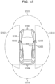
- Fig. 15 is a diagram depicting an example of the installation position of the imaging section 12031.
- the imaging section 12031 includes imaging sections 12101, 12102, 12103, 12104, and 12105.
- the imaging sections 12101, 12102, 12103, 12104, and 12105 are, for example, disposed at positions on a front nose, sideview mirrors, a rear bumper, and a back door of the vehicle 12100 as well as a position on an upper portion of a windshield within the interior of the vehicle.
- the imaging section 12101 provided to the front nose and the imaging section 12105 provided to the upper portion of the windshield within the interior of the vehicle obtain mainly an image of the front of the vehicle 12100.
- the imaging sections 12102 and 12103 provided to the sideview mirrors obtain mainly an image of the sides of the vehicle 12100.
- the imaging section 12104 provided to the rear bumper or the back door obtains mainly an image of the rear of the vehicle 12100.
- the imaging section 12105 provided to the upper portion of the windshield within the interior of the vehicle is used mainly to detect a preceding vehicle, a pedestrian, an obstacle, a signal, a traffic sign, a lane, or the like.
- Fig. 15 depicts an example of photographing ranges of the imaging sections 12101 to 12104.
- An imaging range 12111 represents the imaging range of the imaging section 12101 provided to the front nose.
- An imaging range 1211212113 respectively represents the imaging ranges of the imaging sections 12102 and 12103 provided to the sideview mirrors.
- An imaging range 12114 represents the imaging range of the imaging section 12104 provided to the rear bumper or the back door.
- a bird's-eye image of the vehicle 12100 as viewed from above is obtained by superimposing image data imaged by the imaging sections 12101 to 12104, for example.
- At least one of the imaging sections 12101 to 12104 may have a function of obtaining distance information.
- at least one of the imaging sections 12101 to 12104 may be a stereo camera constituted of a plurality of imaging elements, or may be an imaging element having pixels for phase difference detection.
- the microcomputer 12051 can determine a distance to each three-dimensional object within the imaging ranges 12111 to 12114 and a temporal change in the distance (relative speed with respect to the vehicle 12100) on the basis of the distance information obtained from the imaging sections 12101 to 12104, and thereby extract, as a preceding vehicle, a nearest three-dimensional object in particular that is present on a traveling path of the vehicle 12100 and which travels in substantially the same direction as the vehicle 12100 at a predetermined speed (for example, equal to or more than 0 km/hour). Further, the microcomputer 12051 can set a following distance to be maintained in front of a preceding vehicle in advance, and perform automatic brake control (including following stop control), automatic acceleration control (including following start control), or the like. It is thus possible to perform cooperative control intended for automated driving that makes the vehicle travel automatedly without depending on the operation of the driver or the like.
- automatic brake control including following stop control
- automatic acceleration control including following start control
- the microcomputer 12051 can classify three-dimensional object data on three-dimensional objects into three-dimensional object data of a two-wheeled vehicle, a standard-sized vehicle, a large-sized vehicle, a pedestrian, a utility pole, and other three-dimensional objects on the basis of the distance information obtained from the imaging sections 12101 to 12104, extract the classified three-dimensional object data, and use the extracted three-dimensional object data for automatic avoidance of an obstacle.
- the microcomputer 12051 identifies obstacles around the vehicle 12100 as obstacles that the driver of the vehicle 12100 can recognize visually and obstacles that are difficult for the driver of the vehicle 12100 to recognize visually. Then, the microcomputer 12051 determines a collision risk indicating a risk of collision with each obstacle.
- the microcomputer 12051 In a situation in which the collision risk is equal to or higher than a set value and there is thus a possibility of collision, the microcomputer 12051 outputs a warning to the driver via the audio speaker 12061 or the display section 12062, and performs forced deceleration or avoidance steering via the driving system control unit 12010. The microcomputer 12051 can thereby assist in driving to avoid collision.
- At least one of the imaging sections 12101 to 12104 may be an infrared camera that detects infrared rays.
- the microcomputer 12051 can, for example, recognize a pedestrian by determining whether or not there is a pedestrian in imaged images of the imaging sections 12101 to 12104. Such recognition of a pedestrian is, for example, performed by a procedure of extracting characteristic points in the imaged images of the imaging sections 12101 to 12104 as infrared cameras and a procedure of determining whether or not it is the pedestrian by performing pattern matching processing on a series of characteristic points representing the contour of the object.
- the sound/image output section 12052 controls the display section 12062 so that a square contour line for emphasis is displayed so as to be superimposed on the recognized pedestrian.
- the sound/image output section 12052 may also control the display section 12062 so that an icon or the like representing the pedestrian is displayed at a desired position.
- the technology according to the present disclosure can be applied to, for example, the imaging section 12031 in the configuration described above.
- the distance measuring devices 131 and 131a can be applied to the imaging section 12031.
- the present technology can also be configured as follows.
Landscapes
- Physics & Mathematics (AREA)
- General Physics & Mathematics (AREA)
- Engineering & Computer Science (AREA)
- Radar, Positioning & Navigation (AREA)
- Remote Sensing (AREA)
- Spectroscopy & Molecular Physics (AREA)
- Computer Networks & Wireless Communication (AREA)
- Electromagnetism (AREA)
- Optical Radar Systems And Details Thereof (AREA)
- Measurement Of Optical Distance (AREA)
Abstract
Description
- The present disclosure relates to a photodetection circuit and a distance measuring device.
- As a method of measuring the distance to a subject, a time of flight (ToF) method is used. In the ToF method, reflected light obtained by light emitted from a light source being reflected by a subject is detected. Subsequently, the distance to the subject is measured on the basis of the time from the emission of the light to the detection of the reflected light.
- A distance measuring device using the ToF method is generally provided with a photodetection circuit that detects the reflected light described above. In the photodetection circuit, a voltage change of a photodetection element obtained when photons are incident is detected. A reference voltage for detecting this voltage change is generally fixed.
- Patent Document 1:
Japanese Patent Application Laid-Open No. 2014-81254 - If the reference voltage described above is low, a distance measurement error increases due to characteristic variation of the photodetection element in some cases. In order to reduce this distance measurement error, it is desirable that the reference voltage be high.
- However, if the reference voltage is high, the dead time, which is a period during which photons cannot be detected, becomes long, and the distance measurement accuracy deteriorates in some cases.
- The present disclosure provides a photodetection circuit and a distance measuring device capable of improving distance measuring performance.
- A photodetection circuit according to an embodiment of the present disclosure includes: an avalanche photodiode; a charging circuit that supplies a voltage to the avalanche photodiode; an input amplifier including a comparison circuit in which a voltage level of an output terminal changes according to a comparison result between a voltage of an input terminal connected to the avalanche photodiode and a reference voltage, and a voltage control circuit that changes a potential of the reference voltage; and a state detecting circuit that sets timing for causing the voltage control circuit to change the potential of the reference voltage on the basis of a detection result of the voltage level.
- Furthermore, the comparison circuit may include an inverter circuit, and
the voltage control circuit may include a switching element that is connected to the inverter circuit and performs switching according to an output voltage of the state detecting circuit, and a resistive element or a current source that is connected in parallel with the switching element. - Furthermore, the comparison circuit may include an operational amplifier circuit, and
the voltage control circuit may include a switch circuit that switches the reference voltage to a first reference voltage or a second reference voltage different from the first reference voltage according to an output voltage of the state detecting circuit. - Furthermore, the comparison circuit may include an inverter circuit, and
the voltage control circuit may include a current source that is connected to the inverter circuit and whose output current value changes according to an output voltage of the state detecting circuit. - Furthermore, the state detecting circuit may include inverter elements of odd-numbered stages connected in series with one another.
- Furthermore, the input amplifier may include a first input amplifier that outputs the comparison result to a signal processing circuit, and a second input amplifier that outputs the comparison result to the state detecting circuit.
- Furthermore, circuit configuration of the first input amplifier may be the same as circuit configuration of the second input amplifier.
- Furthermore, circuit configuration of the first input amplifier may be different from circuit configuration of the second input amplifier.
- Furthermore, the avalanche photodiode, the charging circuit, the input amplifier, and the state detecting circuit may be provided on one semiconductor substrate.
- Furthermore, the avalanche photodiode may be provided on a first semiconductor substrate, and the charging circuit, the input amplifier, and the state detecting circuit may be provided on a second semiconductor substrate bonded to the first semiconductor substrate.
- Furthermore, a quench circuit that is connected to the avalanche photodiode and the input terminal of the input amplifier and controls a potential of the input terminal may be further included.
- Furthermore, a cathode of the avalanche photodiode may be connected to the input terminal of the input amplifier.
- Furthermore, an anode of the avalanche photodiode may be connected to the input terminal of the input amplifier.
- A distance measuring device according to an embodiment of the present disclosure includes any one of the above-described photodetection circuits and a signal processing circuit that processes an output signal of the photodetection circuit.
- The signal processing circuit may include:
- a time to digital converter (TDC) that converts the output signal into a digital value; and
- a histogram creating circuit that counts the number of times the digital value is acquired; and
- a distance determining section that determines a distance from the photodetection circuit to a subject on the basis of a count result of the histogram creating circuit.
-
-
Fig. 1 is a block diagram depicting a configuration example of an imaging system using a photodetection circuit and a distance measuring device according to a first embodiment. -
Fig. 2 is a block diagram depicting a configuration example of the photodetection circuit and the signal processing circuit. -
Fig. 3A is a circuit diagram depicting configuration of an input amplifier according to the first embodiment. -
Fig. 3B is a circuit diagram depicting configuration of a first modification of the input amplifier. -
Fig. 4 is a circuit diagram depicting configuration of a second modification of the input amplifier. -
Fig. 5 is a circuit diagram depicting configuration of a third modification of the input amplifier. -
Fig. 6A is a circuit diagram depicting configuration of a fourth modification of the input amplifier. -
Fig. 6B is a circuit diagram depicting configuration of a fifth modification of the input amplifier. -
Fig. 7 is a circuit diagram depicting configuration of a state detecting circuit. -
Fig. 8 is a graph depicting an example of voltage characteristics of a plurality of photodetection elements. -
Fig. 9 is a graph depicting an example of voltage characteristics of a single photodetection element. -
Fig. 10 is a graph depicting voltage characteristics of the photodetection element and reference voltage characteristics of the input amplifier. -
Fig. 11 is a perspective view depicting a structure of a distance measuring device according to a modification. -
Fig. 12 is a block diagram depicting a configuration example of a distance measuring device according to a second embodiment. -
Fig. 13 is a graph depicting voltage characteristics of the photodetection element and reference voltage characteristics of the input amplifier. -
Fig. 14 is a block diagram depicting an example of schematic configuration of a vehicle control system. -
Fig. 15 is a diagram of assistance in explaining an example of installation positions of an outside-vehicle information detecting section and an imaging section. -
Fig. 1 is a block diagram depicting a configuration example of an imaging system using a photodetection circuit and a distance measuring device according to a first embodiment. Animaging system 101 depicted inFig. 1 is a system that captures a distance image using the ToF method, and includes anillumination device 111 and animaging device 112. - The
illumination device 111 includes anillumination control section 121 and alight source 122. Theillumination control section 121 controls a pattern in which thelight source 122 emits irradiation light on the basis of control of thecontrol section 132 of theimaging device 112. Specifically, theillumination control section 121 controls the pattern in which thelight source 122 emits irradiation light according to the irradiation code included in the irradiation signal supplied from thecontrol section 132. For example, the irradiation code includes two values of "1" (High) and "0" (Low). Theillumination control section 121 turns on thelight source 122 when the value of the irradiation code is "1", and turns off thelight source 122 when the value of the irradiation code is "0". - The
light source 122 emits light (irradiation light) in a predetermined wavelength range on the basis of control of theillumination control section 121. Thelight source 122 is, for example, an infrared laser diode. The type of thelight source 122 and the wavelength range of the irradiation light can be arbitrarily set according to the application of theimaging system 101 or the like. - The
imaging device 112 receives reflected light obtained by irradiation light being reflected by a subject 102 and a subject 103. Theimaging device 112 includes a distance measuring device 131, thecontrol section 132, adisplay section 133, and astorage section 134. - The distance measuring device 131 includes a
lens 141, aphotodetection circuit 142, and asignal processing circuit 143. Thelens 141 forms an image of the incident light on thephotodetection circuit 142. Incidentally, thelens 141 has any configuration, and for example, thelens 141 can include a plurality of lens groups. - The
photodetection circuit 142 images the subject 102, the subject 103, and the like on the basis of control of thecontrol section 132. Furthermore, thephotodetection circuit 142 outputs a signal obtained by imaging to thesignal processing circuit 143. - The
signal processing circuit 143 processes the output signal of thephotodetection circuit 142 on the basis of control of thecontrol section 132. For example, thesignal processing circuit 143 detects the distance to the subject on the basis of the output signal of thephotodetection circuit 142 and creates a distance image indicating the distance to the subject. - The
control section 132 includes, for example, a control circuit such as a field programmable gate array (FPGA) or a digital signal processor (DSP), a processor, or the like. Thecontrol section 132 controls theillumination control section 121, thephotodetection circuit 142, and thesignal processing circuit 143. - The
display section 133 includes, for example, a panel type display device such as a liquid crystal display device or an organic electro luminescence (EL) display device. - The
storage section 134 can include any storage device, storage medium, or the like, and stores a distance image or the like. -
Fig. 2 is a block diagram depicting a configuration example of thephotodetection circuit 142 and thesignal processing circuit 143. - The
photodetection circuit 142 includes aphotodetection element 151, a chargingcircuit 152, a quenchcircuit 153, aninput amplifier 154, and astate detecting circuit 155. These are provided on one semiconductor substrate. Incidentally, since thephotodetection circuit 142 depicted inFig. 2 is a unit circuit corresponding to one pixel, the distance measuring device 131 includes a plurality ofphotodetection circuits 142 according to the number of pixels. - The
photodetection element 151 is a photodiode a typical example of which is an avalanche photo diode (APD), a single photon avalanche diode (SPAD), or the like. The cathode of thephotodetection element 151 is connected to the chargingcircuit 152 and an input terminal of theinput amplifier 154. The anode of thephotodetection element 151 is set to a negative voltage VRL by a negative power supply (not illustrated). - The charging
circuit 152 includes, for example, a current source and a resistive element connected in series with each other. The chargingcircuit 152 supplies a positive voltage to the cathode of thephotodetection element 151. As a result, if a reverse voltage equal to or higher than the breakdown voltage is applied between the anode and the cathode of thephotodetection element 151, thephotodetection element 151 is set to the Geiger mode. If photons are incident on thephotodetection element 151 set to the Geiger mode, avalanche multiplication occurs, and a current flows through thephotodetection element 151. - The quench
circuit 153 includes, for example, an N-channel MOS transistor 156. The drain of the N-channel MOS transistor 156 is connected to the cathode of thephotodetection element 151 and the input terminal of theinput amplifier 154, and the source is grounded. If an external signal APDEN is input to the gate of the N-channel MOS transistor 156, a cathode voltage Vc is forcibly set to the ground potential. In this case, the photodetection function of thephotodetection element 151 is deteriorated. Therefore, it is possible to avoid erroneous detection of an after-pulse in which avalanche multiplication occurs again even though no photon is incident on thephotodetection element 151, or the like. Incidentally, the quenchcircuit 153 is not limited to the N-channel MOS transistor 156 as long as the cathode voltage Vc can be forcibly set to a potential that lowers the photodetection function of thephotodetection element 151. - Incidentally, the source of the N-
channel MOS transistor 156 may be connected to a negative potential instead of being grounded. In this case, there is a concern that the rise of the recharge (recovery) of the cathode voltage Vc becomes slower and the dead time becomes longer. However, as will be described later, in the present embodiment, the dead time can be shortened by optimizing the reference voltage of theinput amplifier 154. - The
input amplifier 154 compares the voltage of the input terminal, in other words, the cathode voltage Vc of thephotodetection element 151, with a variable reference voltage. Furthermore, in theinput amplifier 154, the voltage level of the output terminal changes according to the comparison result. The circuit configuration of theinput amplifier 154 will be described later. - The
state detecting circuit 155 detects the voltage level of the output terminal of theinput amplifier 154 and sets the timing to change the potential of the reference voltage described above. The configuration of thestate detecting circuit 155 will also be described later. - The
signal processing circuit 143 includes a time to digital converter (TDC) 200, ahistogram creating section 201, and adistance determining section 202. The time to digital converter (TDC) 200 converts an output signal of theinput amplifier 154 into a digital value. Specifically, theTDC 200 digitally converts the occurrence time of the transition timing of the voltage level of the output terminal of theinput amplifier 154. - The
histogram creating section 201 counts the number of times the digital value described above is acquired, that is, the number of times thephotodetection element 151 reacts. - The
distance determining section 202 determines the distance from thephotodetection element 151 to the subject 102, 103 on the basis of the count result of thehistogram creating section 201. For example, thedistance determining section 202 calculates an approximate curve for a normal distribution indicating the count result of the histogram creating section 201 (so-called Gaussian fitting), and obtains the distance by using the approximate curve. - Hereinafter, the circuit configuration of the
input amplifier 154 will be described. -
Fig. 3A is a circuit diagram depicting configuration of the input amplifier according to the present embodiment. Theinput amplifier 154 according to the present embodiment includes aninverter circuit 161 and avoltage control circuit 162 connected to theinverter circuit 161. Theinverter circuit 161 corresponds to a comparison circuit. - The
inverter circuit 161 includesMOS transistors 170 to 173. TheMOS transistor 170 and theMOS transistor 172 are P-channel MOS transistors, and theMOS transistor 171 and theMOS transistor 173 are N-channel MOS transistors. TheMOS transistor 170 and theMOS transistor 171 are connected in series. Furthermore, theMOS transistor 172 and theMOS transistor 173 are connected in series. - Each of the gates of the
MOS transistor 170 and theMOS transistor 171 is an input terminal of theinput amplifier 154. The cathode voltage Vc of thephotodetection element 151 is input to each of the gates. The source of theMOS transistor 170 is connected to a positive power supply, and the source of theMOS transistor 171 is connected to thevoltage control circuit 162. Each of the drains of theMOS transistor 170 and theMOS transistor 171 is connected to each of the gates of theMOS transistor 172 and theMOS transistor 173. The source of theMOS transistor 172 is connected to a positive power supply, and the source of theMOS transistor 171 is grounded. Each of the drains of theMOS transistor 172 and theMOS transistor 173 is an output terminal of theinput amplifier 154, and is connected to thestate detecting circuit 155 and thesignal processing circuit 143. - The
voltage control circuit 162 includes aswitching element 174 and aresistive element 175. The switchingelement 174 is, for example, an N-channel MOS transistor. An output voltage Vo of thestate detecting circuit 155 is input to the gate of theswitching element 174. The drain is connected to the source of theMOS transistor 171. The source is grounded. In contrast, theresistive element 175 is connected in parallel to theswitching element 174. - In the
inverter circuit 161 configured as described above, one of theMOS transistor 170 or theMOS transistor 171 is turned on and the other is turned off according to the potential of the cathode voltage Vc of thephotodetection element 151. If theMOS transistor 170 is turned on, theMOS transistor 173 is turned on, and theMOS transistor 172 is turned off. In this case, a voltage level Vs becomes a low level. If theMOS transistor 171 is turned on, theMOS transistor 172 is turned on, and theMOS transistor 173 is turned off. In this case, the voltage level Vs becomes a high level. - The threshold voltage for switching the voltage level Vs to the high level or the low level corresponds to the potential of the reference voltage. The potential of the reference voltage is changed by the
voltage control circuit 162. If theswitching element 174 of thevoltage control circuit 162 is turned on, the potential of the reference voltage decreases. Conversely, if theswitching element 174 is turned off, the potential of the reference voltage increases. -
Fig. 3B is a circuit diagram depicting configuration of a first modification of theinput amplifier 154. Components similar to those of theinput amplifier 154 illustrated inFig. 3A are denoted by the same reference numerals, and a detailed description thereof will be omitted. Aninput amplifier 154 illustrated inFig. 3B is different from theinput amplifier 154 illustrated inFig. 3A in the configuration of the voltage control circuit. Specifically, in avoltage control circuit 162a according to the present modification, acurrent source 175a is provided instead of theresistive element 175. Thecurrent source 175a is an N-channel MOS transistor. The drain of the N-channel MOS transistor is connected to the drain of theswitching element 174, and the source is grounded. Furthermore, a reference voltage is input to the gate. This reference voltage is set such that the on-resistance of theswitching element 174 is lower than the on-resistance of thecurrent source 175a. -
Fig. 4 is a circuit diagram depicting configuration of a second modification of theinput amplifier 154. Aninput amplifier 154a according to the present modification includes aninverter circuit 161a and avoltage control circuit 163 connected to theinverter circuit 161a. Similarly to theinverter circuit 161 depicted inFig. 3A , theinverter circuit 161a includesMOS transistors 170a to 173a, and thus a detailed description thereof will be omitted. - In contrast, the
voltage control circuit 163 includes acurrent source 176a, aswitch 176b, aswitch 176c, and aninverter element 176d. Thecurrent source 176a is an N-channel MOS transistor. Theswitch 176b and theswitch 176c are connected in parallel with each other to the gate of the N-channel MOS transistor. The drain is connected to the source of theMOS transistor 171a. The source is grounded. The output current value of thecurrent source 176a changes according to the gate voltage of the N-channel MOS transistor. If the gate voltage decreases, the output current value decreases, and therefore, the reference voltage for switching the voltage level Vs of theinverter circuit 161a increases. Conversely, if the gate voltage increases, the output current value increases, and therefore, the reference voltage decreases. Theswitch 176b and theswitch 176c are turned on or off on the basis of the output voltage Vo of thestate detecting circuit 155. A voltage obtained by inverting the potential of the output voltage Vo by theinverter element 176d is input to theswitch 176c. Therefore, if one of theswitch 176b or theswitch 176c is turned on, the other is turned off. If theswitch 176b is turned on, a first reference voltage Vref1 is supplied to thecurrent source 176a as the gate voltage described above. Conversely, if theswitch 176c is turned on, a second reference voltage Vref2 having a potential different from that of the first reference voltage Vref1 is supplied to thecurrent source 176a as the gate voltage described above. Incidentally, theinverter element 176d may be provided on theswitch 176b side instead of theswitch 176c side. -
Fig. 5 is a circuit diagram depicting configuration of a third modification of theinput amplifier 154. Aninput amplifier 154b according to the present modification includes anoperational amplifier circuit 164 and aswitch circuit 165. Theoperational amplifier circuit 164 is an example of the comparison circuit and includesMOS transistors 177 to 180 and acurrent source 181. TheMOS transistor 177 and theMOS transistor 178 are P-channel MOS transistors and constitute a current mirror circuit. TheMOS transistor 179 and theMOS transistor 180 are N-channel MOS transistors having the same size and the same electrical characteristics, and are connected in parallel with each other via the current mirror circuit described above. The gate of theMOS transistor 179 is an input terminal of theinput amplifier 154b. Furthermore, the drains of theMOS transistor 178 and theMOS transistor 180 are output terminals of theinput amplifier 154b. Thecurrent source 181 is connected to each of the sources of theMOS transistor 179 and theMOS transistor 180. - The
switch circuit 165 is a modification of thevoltage control circuit 162, and includes a switch 182, aswitch 183, and aninverter element 184. The switch 182 and theswitch 183 are turned on or off on the basis of the output voltage Vo of thestate detecting circuit 155. A voltage obtained by inverting the potential of the output voltage Vo by theinverter element 184 is input to theswitch 183. Therefore, if one of the switch 182 or theswitch 183 is turned on, the other is turned off. If the switch 182 is turned on, the first reference voltage Vref1 is input to the gate of theMOS transistor 180. Conversely, if theswitch 183 is turned on, the second reference voltage Vref2 having a potential different from that of the first reference voltage Vref1 is input to the gate of theMOS transistor 180. Incidentally, theinverter element 184 may be provided on the switch 182 side instead of theswitch 183 side. -
Fig. 6A is a circuit diagram depicting configuration of a fourth modification of theinput amplifier 154. The present modification includes afirst input amplifier 154c and asecond input amplifier 154d. Similarly to theinput amplifier 154 illustrated inFig. 3A , thefirst input amplifier 154c includesMOS transistors 170c to 173c, aswitching element 174c, and aresistive element 175c. In thefirst input amplifier 154c, the gate of theMOS transistor 170c is an input terminal, and each of the drains of theMOS transistor 172c and theMOS transistor 173c is an output terminal. This output terminal is connected to thesignal processing circuit 143. - In contrast, similarly to the
input amplifier 154, thesecond input amplifier 154d also includesMOS transistors 170d to 173d, aswitching element 174d, and aresistive element 175d. In thesecond input amplifier 154d, the gate of theMOS transistor 170d is an input terminal, and each of the drains of theMOS transistor 172d and theMOS transistor 173d is an output terminal. This output terminal is connected to thestate detecting circuit 155. - Incidentally, in the present modification, the circuit configuration of the
first input amplifier 154c is the same as the circuit configuration of thesecond input amplifier 154d, but may be different. -
Fig. 6B is a circuit diagram depicting configuration of a fifth modification of theinput amplifier 154. Components similar to those inFig. 6A are denoted by the same reference numerals, and a detailed description thereof will be omitted. In the present modification, configuration of thesecond input amplifier 154d is different from that ofFig. 6A . Thesecond input amplifier 154d according to the present modification is not provided with theswitching element 174d and theresistive element 175d, and the source of theMOS transistor 171d is grounded. That is, thesecond input amplifier 154d does not perform reference voltage control based on the output voltage Vo of thestate detecting circuit 155. According to the present modification, since the cathode voltage Vc input during operation of thestate detecting circuit 155 becomes constant, control is stabilized. - Hereinafter, circuit configuration of the
state detecting circuit 155 will be described. -
Fig. 7 is a circuit diagram depicting configuration of thestate detecting circuit 155. Thestate detecting circuit 155 depicted inFig. 7 can be applied to theinput amplifier 154 depicted inFigs. 3A and 3B , theinput amplifier 154b depicted inFig. 5 , and thesecond input amplifier 154d depicted inFigs. 6A and6B . Thisstate detecting circuit 155 includes five stages ofinverter elements 190 connected in series with one another. - The
state detecting circuit 155 described above outputs an input signal after a predetermined time has elapsed. The predetermined time corresponds to a delay time between the input signal and the output signal. This delay time can be set on the basis of the number of stages of theinverter elements 190. Therefore, the number of stages of theinverter elements 190 is not limited to five, and it is sufficient if the number is an odd number. By adjusting the number of stages of theinverter elements 190, the timing of changing the reference voltage of each input amplifier can be set. -
Fig. 8 is a graph depicting an example of voltage characteristics of a plurality ofphotodetection elements 151. In the graph illustrated inFig. 8 , the horizontal axis represents time, and the vertical axis represents the cathode voltage Vc of the photodetection element. In a pixel array in which the plurality ofphotodetection elements 151 is two-dimensionally arranged, the drop characteristic of the cathode voltage Vc obtained when photons are incident on thephotodetection element 151 is different between the photodetection elements in some cases due to variations in on-resistance and parasitic capacitance. In this case, as depicted inFig. 8 , if the reference voltage Vref of the input amplifier is fixed to a low value, the timing of detecting the drop of the cathode voltage Vc varies, which can be a factor of a distance measurement error. In order to reduce this distance measurement error, it is desirable to set the reference voltage Vref to a high value. -
Fig. 9 is a graph depicting an example of voltage characteristics of asingle photodetection element 151. Also in the graph illustrated inFig. 9 , the horizontal axis represents time, and the vertical axis represents the cathode voltage Vc of thephotodetection element 151. If photons are incident on thephotodetection element 151, avalanche multiplication occurs, and a current flows through thephotodetection element 151. As a result, the cathode voltage Vc drops. If the avalanche multiplication converges, the cathode voltage Vc gradually recovers. In a dead time Tdead which is a period from when the cathode voltage Vc drops to when the cathode voltage Vc recovers, photons cannot be detected. Therefore, if the reference voltage Vref is fixed to a high value, the dead time Tdead becomes long, and the distance measuring performance can be insufficient. Therefore, in order to shorten the dead time Tdead, it is desirable to set the reference voltage Vref to a low value. -
Fig. 10 is a graph depicting voltage characteristics of thephotodetection element 151 and reference voltage characteristics of theinput amplifier 154. Also in the graph illustrated inFig. 10 , the horizontal axis represents time, and the vertical axis represents the cathode voltage Vc of thephotodetection element 151. - In the
input amplifier 154 according to the present embodiment, as described above, thevoltage control circuit 162 can set two reference voltages. Furthermore, thestate detecting circuit 155 can set a timing to switch between the two reference voltages. Therefore, as illustrated inFig. 10 , drop of the cathode voltage Vc can be detected at the first reference voltage Vref1 having a high potential, and recovery of the cathode voltage Vc can be detected at the second reference voltage Vref2 having a low potential. Incidentally, in the present embodiment, the timing at which thestate detecting circuit 155 switches from the first reference voltage Vref1 to the second reference voltage Vref2 is matched with the timing from fall to rise of the cathode voltage Vc. Therefore, it is possible to more accurately measure drop and recovery of the cathode voltage Vc. - According to the present embodiment described above, since the reference voltage for detecting drop of the cathode voltage Vc of the
photodetection element 151 can be set high, it is possible to reduce a distance measurement error due to variation in output timing among the plurality ofphotodetection elements 151. Furthermore, since the reference voltage for detecting recovery of the cathode voltage Vc can be set low, the dead time can be shortened. Therefore, since the two conflicting requirements of early detection of drop and recovery of the cathode voltage Vc can be satisfied, it is possible to improve the distance measuring performance. -
Fig. 11 is a perspective view depicting a structure of a distance measuring device according to a modification. Incidentally, components similar to those of the distance measuring device 131 according to the first embodiment described above are denoted by the same reference numerals, and detailed description thereof will be omitted. - A
distance measuring device 131a depicted inFig. 11 includes afirst semiconductor substrate 301 and asecond semiconductor substrate 302. Thefirst semiconductor substrate 301 and thesecond semiconductor substrate 302 are bonded by, for example, a copper pad and are electrically connected. - On the
first semiconductor substrate 301, a pixel array is formed by two-dimensionally arranging the plurality ofphotodetection elements 151. The surface on which thephotodetection elements 151 are formed becomes a light receiving surface S of thedistance measuring device 131a. - The
second semiconductor substrate 302 has aregion 312 facing thefirst semiconductor substrate 301 and aregion 322 adjacent to theregion 312. In theregion 312, peripheral components of thephotodetection element 151 in thephotodetection circuit 142, that is, the chargingcircuit 152, the quenchcircuit 153, theinput amplifier 154, and thestate detecting circuit 155 are formed. In contrast, thesignal processing circuit 143 is formed in theregion 322. - Even in the structure of the present modification described above, similarly to the first embodiment, the reference voltage for detecting drop of the cathode voltage Vc of the
photodetection element 151 and the reference voltage for detecting recovery of the cathode voltage Vc can be separately set. Therefore, the distance measuring performance can be improved. -
Fig. 12 is a block diagram depicting a configuration example of a distance measuring device according to a second embodiment. Components similar to those of the distance measuring device 131 according to the first embodiment described above are denoted by the same reference numerals, and detailed description thereof will be omitted. The distance measuring device according to the present embodiment is different from that according to the first embodiment in configuration of a photodetection circuit. Hereinafter, the photodetection circuit according to the present embodiment will be described. - In a
photodetection circuit 144 illustrated inFig. 12 , the anode of thephotodetection element 151 is connected to the input terminal of theinput amplifier 154, and the cathode is connected to a power supply. Therefore, theinput amplifier 154 detects an increase and recovery of an anode voltage Va of thephotodetection element 151 on the basis of the comparison between the anode voltage Va and the reference voltage. Since the circuit configuration of theinput amplifier 154 is similar to that of the first embodiment, the reference voltage is switched on the basis of control of thestate detecting circuit 155. -
Fig. 13 is a graph depicting voltage characteristics of thephotodetection element 151 and reference voltage characteristics of theinput amplifier 154. In the graph depicted inFig. 13 , the horizontal axis represents time, and the vertical axis represents the anode voltage Va of thephotodetection element 151. - In the present embodiment, if photons are incident on the
photodetection element 151, the anode voltage Va increases. Thereafter, the anode voltage Va gradually drops (recovers). At this time, in theinput amplifier 154, thevoltage control circuit 162 switches between the two reference voltages on the basis of control of thestate detecting circuit 155. Therefore, as illustrated inFig. 13 , an increase in the anode voltage Va can be detected at the first reference voltage having a low potential, and a decrease in the anode voltage Va can be detected at the second reference voltage Vref2 having a high potential. Therefore, it is possible to reduce a distance measurement error due to variation in output timing among the plurality ofphotodetection elements 151 and to shorten the dead time Tdead. - According to the present embodiment described above, the reference voltage for detecting an increase in the anode voltage Va of the
photodetection element 151 and the reference voltage for detecting a decrease in the anode voltage Va can be set separately. Therefore, the distance measuring performance can be improved. - The technology according to the present disclosure (the present technology) can be applied to various products. For example, the technology according to the present disclosure may be realized as a device mounted on any type of a mobile body such as an automobile, an electric car, a hybrid electric car, a motorcycle, a bicycle, a personal mobility vehicle, an airplane, a drone, a ship, or a robot.
-
Fig. 14 is a block diagram depicting an example of schematic configuration of a vehicle control system as an example of a mobile body control system to which the technology according to an embodiment of the present disclosure can be applied. - The
vehicle control system 12000 includes a plurality of electronic control units connected to each other via acommunication network 12001. In the example depicted inFig. 14 , thevehicle control system 12000 includes a drivingsystem control unit 12010, a bodysystem control unit 12020, an outside-vehicleinformation detecting unit 12030, an in-vehicleinformation detecting unit 12040, and anintegrated control unit 12050. In addition, amicrocomputer 12051, a sound/image output section 12052, and a vehicle-mounted network interface (I/F) 12053 are illustrated as a functional configuration of theintegrated control unit 12050. - The driving
system control unit 12010 controls the operation of devices related to the driving system of the vehicle in accordance with various kinds of programs. For example, the drivingsystem control unit 12010 functions as a control device for a driving force generating device for generating the driving force of the vehicle, such as an internal combustion engine, a driving motor, or the like, a driving force transmitting mechanism for transmitting the driving force to wheels, a steering mechanism for adjusting the steering angle of the vehicle, a braking device for generating the braking force of the vehicle, and the like. - The body
system control unit 12020 controls the operation of various kinds of devices provided to a vehicle body in accordance with various kinds of programs. For example, the bodysystem control unit 12020 functions as a control device for a keyless entry system, a smart key system, a power window device, or various kinds of lamps such as a headlamp, a backup lamp, a brake lamp, a turn signal, a fog lamp, or the like. In this case, radio waves transmitted from a mobile device as an alternative to a key or signals of various kinds of switches can be input to the bodysystem control unit 12020. The bodysystem control unit 12020 receives these input radio waves or signals, and controls a door lock device, the power window device, the lamps, or the like of the vehicle. - The outside-vehicle
information detecting unit 12030 detects information about the outside of the vehicle including thevehicle control system 12000. For example, the outside-vehicleinformation detecting unit 12030 is connected with animaging section 12031. The outside-vehicleinformation detecting unit 12030 makes theimaging section 12031 image an image of the outside of the vehicle, and receives the imaged image. On the basis of the received image, the outside-vehicleinformation detecting unit 12030 may perform processing of detecting an object such as a human, a vehicle, an obstacle, a sign, a character on a road surface, or the like, or processing of detecting a distance thereto. - The
imaging section 12031 is an optical sensor that receives light, and which outputs an electric signal corresponding to a received light amount of the light. Theimaging section 12031 can output the electric signal as an image, or can output the electric signal as information about a measured distance. In addition, the light received by theimaging section 12031 may be visible light, or may be invisible light such as infrared rays or the like. - The in-vehicle
information detecting unit 12040 detects information about the inside of the vehicle. The in-vehicleinformation detecting unit 12040 is, for example, connected with a driverstate detecting section 12041 that detects the state of a driver. The driverstate detecting section 12041, for example, includes a camera that images the driver. On the basis of detection information input from the driverstate detecting section 12041, the in-vehicleinformation detecting unit 12040 may calculate a degree of fatigue of the driver or a degree of concentration of the driver, or may determine whether the driver is dozing. - The
microcomputer 12051 can calculate a control target value for the driving force generating device, the steering mechanism, or the braking device on the basis of the information about the inside or outside of the vehicle which information is obtained by the outside-vehicleinformation detecting unit 12030 or the in-vehicleinformation detecting unit 12040, and output a control command to the drivingsystem control unit 12010. For example, themicrocomputer 12051 can perform cooperative control intended to implement functions of an advanced driver assistance system (ADAS) which functions include collision avoidance or shock mitigation for the vehicle, following driving based on a following distance, vehicle speed maintaining driving, a warning of collision of the vehicle, a warning of deviation of the vehicle from a lane, or the like. - In addition, the
microcomputer 12051 can perform cooperative control intended for automated driving, which makes the vehicle to travel automatedly without depending on the operation of the driver, or the like, by controlling the driving force generating device, the steering mechanism, the braking device, or the like on the basis of the information about the outside or inside of the vehicle which information is obtained by the outside-vehicleinformation detecting unit 12030 or the in-vehicleinformation detecting unit 12040. - In addition, the
microcomputer 12051 can output a control command to the bodysystem control unit 12020 on the basis of the information about the outside of the vehicle which information is obtained by the outside-vehicleinformation detecting unit 12030. For example, themicrocomputer 12051 can perform cooperative control intended to prevent a glare by controlling the headlamp so as to change from a high beam to a low beam, for example, in accordance with the position of a preceding vehicle or an oncoming vehicle detected by the outside-vehicleinformation detecting unit 12030. - The sound/
image output section 12052 transmits an output signal of at least one of a sound and an image to an output device capable of visually or auditorily notifying information to an occupant of the vehicle or the outside of the vehicle. In the example ofFig. 14 , anaudio speaker 12061, adisplay section 12062, and aninstrument panel 12063 are illustrated as the output device. Thedisplay section 12062 may, for example, include at least one of an on-board display and a head-up display. -
Fig. 15 is a diagram depicting an example of the installation position of theimaging section 12031. - In
Fig. 15 , theimaging section 12031 includesimaging sections - The
imaging sections vehicle 12100 as well as a position on an upper portion of a windshield within the interior of the vehicle. Theimaging section 12101 provided to the front nose and theimaging section 12105 provided to the upper portion of the windshield within the interior of the vehicle obtain mainly an image of the front of thevehicle 12100. Theimaging sections vehicle 12100. Theimaging section 12104 provided to the rear bumper or the back door obtains mainly an image of the rear of thevehicle 12100. Theimaging section 12105 provided to the upper portion of the windshield within the interior of the vehicle is used mainly to detect a preceding vehicle, a pedestrian, an obstacle, a signal, a traffic sign, a lane, or the like. - Incidentally,
Fig. 15 depicts an example of photographing ranges of theimaging sections 12101 to 12104. Animaging range 12111 represents the imaging range of theimaging section 12101 provided to the front nose. An imaging range 1211212113 respectively represents the imaging ranges of theimaging sections imaging range 12114 represents the imaging range of theimaging section 12104 provided to the rear bumper or the back door. A bird's-eye image of thevehicle 12100 as viewed from above is obtained by superimposing image data imaged by theimaging sections 12101 to 12104, for example. - At least one of the
imaging sections 12101 to 12104 may have a function of obtaining distance information. For example, at least one of theimaging sections 12101 to 12104 may be a stereo camera constituted of a plurality of imaging elements, or may be an imaging element having pixels for phase difference detection. - For example, the
microcomputer 12051 can determine a distance to each three-dimensional object within the imaging ranges 12111 to 12114 and a temporal change in the distance (relative speed with respect to the vehicle 12100) on the basis of the distance information obtained from theimaging sections 12101 to 12104, and thereby extract, as a preceding vehicle, a nearest three-dimensional object in particular that is present on a traveling path of thevehicle 12100 and which travels in substantially the same direction as thevehicle 12100 at a predetermined speed (for example, equal to or more than 0 km/hour). Further, themicrocomputer 12051 can set a following distance to be maintained in front of a preceding vehicle in advance, and perform automatic brake control (including following stop control), automatic acceleration control (including following start control), or the like. It is thus possible to perform cooperative control intended for automated driving that makes the vehicle travel automatedly without depending on the operation of the driver or the like. - For example, the
microcomputer 12051 can classify three-dimensional object data on three-dimensional objects into three-dimensional object data of a two-wheeled vehicle, a standard-sized vehicle, a large-sized vehicle, a pedestrian, a utility pole, and other three-dimensional objects on the basis of the distance information obtained from theimaging sections 12101 to 12104, extract the classified three-dimensional object data, and use the extracted three-dimensional object data for automatic avoidance of an obstacle. For example, themicrocomputer 12051 identifies obstacles around thevehicle 12100 as obstacles that the driver of thevehicle 12100 can recognize visually and obstacles that are difficult for the driver of thevehicle 12100 to recognize visually. Then, themicrocomputer 12051 determines a collision risk indicating a risk of collision with each obstacle. In a situation in which the collision risk is equal to or higher than a set value and there is thus a possibility of collision, themicrocomputer 12051 outputs a warning to the driver via theaudio speaker 12061 or thedisplay section 12062, and performs forced deceleration or avoidance steering via the drivingsystem control unit 12010. Themicrocomputer 12051 can thereby assist in driving to avoid collision. - At least one of the
imaging sections 12101 to 12104 may be an infrared camera that detects infrared rays. Themicrocomputer 12051 can, for example, recognize a pedestrian by determining whether or not there is a pedestrian in imaged images of theimaging sections 12101 to 12104. Such recognition of a pedestrian is, for example, performed by a procedure of extracting characteristic points in the imaged images of theimaging sections 12101 to 12104 as infrared cameras and a procedure of determining whether or not it is the pedestrian by performing pattern matching processing on a series of characteristic points representing the contour of the object. When themicrocomputer 12051 determines that there is a pedestrian in the imaged images of theimaging sections 12101 to 12104, and thus recognizes the pedestrian, the sound/image output section 12052 controls thedisplay section 12062 so that a square contour line for emphasis is displayed so as to be superimposed on the recognized pedestrian. The sound/image output section 12052 may also control thedisplay section 12062 so that an icon or the like representing the pedestrian is displayed at a desired position. - An example of the vehicle control system to which the technology according to the present disclosure can be applied has been described above. The technology according to the present disclosure can be applied to, for example, the
imaging section 12031 in the configuration described above. Specifically, thedistance measuring devices 131 and 131a can be applied to theimaging section 12031. By applying the technology according to the present disclosure, a captured image with higher distance measurement accuracy can be obtained, and therefore, safety can be improved. - Incidentally, the present technology can also be configured as follows.
- (1) A photodetection circuit including:
- an avalanche photodiode;
- a charging circuit that supplies a voltage to the avalanche photodiode;
- an input amplifier including a comparison circuit in which a voltage level of an output terminal changes according to a comparison result between a voltage of an input terminal connected to the avalanche photodiode and a reference voltage, and a voltage control circuit that changes a potential of the reference voltage; and
- a state detecting circuit that sets timing for causing the voltage control circuit to change the potential of the reference voltage on the basis of a detection result of the voltage level.
- (2) The photodetection circuit according to (1),
- in which the comparison circuit includes an inverter circuit, and
- the voltage control circuit includes a switching element that is connected to the inverter circuit and performs switching according to an output voltage of the state detecting circuit, and a resistive element or a current source that is connected in parallel with the switching element.
- (3) The photodetection circuit according to (1),
- in which the comparison circuit includes an operational amplifier circuit, and
- the voltage control circuit includes a switch circuit that switches the reference voltage to a first reference voltage or a second reference voltage different from the first reference voltage according to an output voltage of the state detecting circuit.
- (4) The photodetection circuit according to (1),
- in which the comparison circuit includes an inverter circuit, and
- the voltage control circuit includes a current source that is connected to the inverter circuit and whose output current value changes according to an output voltage of the state detecting circuit.
- (5) The photodetection circuit according to (2) or (3), in which the state detecting circuit includes inverter elements of odd-numbered stages connected in series with one another.
- (6) The photodetection circuit according to any one of (1) to (5), in which the input amplifier includes a first input amplifier that outputs the comparison result to a signal processing circuit, and a second input amplifier that outputs the comparison result to the state detecting circuit.
- (7) The photodetection circuit according to (6), in which circuit configuration of the first input amplifier is the same as circuit configuration of the second input amplifier.
- (8) The photodetection circuit according to (6), in which circuit configuration of the first input amplifier is different from circuit configuration of the second input amplifier.
- (9) The photodetection circuit according to any one of (1) to (8), in which the avalanche photodiode, the charging circuit, the input amplifier, and the state detecting circuit are provided on one semiconductor substrate.
- (10) The photodetection circuit according to any one of (1) to (8), in which the avalanche photodiode is provided on a first semiconductor substrate, and the charging circuit, the input amplifier, and the state detecting circuit are provided on a second semiconductor substrate bonded to the first semiconductor substrate.
- (11) The photodetection circuit according to any one of (1) to (10) further including a quench circuit that is connected to the avalanche photodiode and the input terminal of the input amplifier and controls a potential of the input terminal.
- (12) The photodetection circuit according to any one of (1) to (11), in which a cathode of the avalanche photodiode is connected to the input terminal of the input amplifier.
- (13) The photodetection circuit according to any one of (1) to (11), in which an anode of the avalanche photodiode is connected to the input terminal of the input amplifier.
- (14) A distance measuring device including:
- the photodetection circuit according to any one of (1) to (13); and
- a signal processing circuit that processes an output signal of the photodetection circuit.
- (15) The distance measuring device according to (14),
in which the signal processing circuit includes:- a time to digital converter (TDC) that converts the output signal into a digital value;
- a histogram creating circuit that counts the number of times the digital value is acquired; and
- a distance determining section that determines a distance from the photodetection circuit to a subject on the basis of a count result of the histogram creating circuit.
-
- 142
- Photodetection circuit
- 143
- Signal processing circuit
- 151
- Photodetection element
- 152
- Charging circuit
- 153
- Quench circuit
- 154, 154a, 154b
- Input amplifier
- 154c
- First input amplifier
- 154d
- Second input amplifier
- 155
- State detecting circuit
- 161, 161a
- Inverter circuit
- 162
- Voltage control circuit
- 163
- Voltage control circuit
- 164
- Operational amplifier circuit
- 165
- Switch circuit
- 174
- Switching element
- 175
- Resistive element
- 175a
- Current source
- 190
- Inverter element
- 191
- Operational amplifier
- 200
- TDC
- 201
- Histogram creating section
- 202
- Distance determining section
- 301
- First semiconductor substrate
- 302
- Second semiconductor substrate
Claims (15)
- A photodetection circuit comprising:an avalanche photodiode;a charging circuit that supplies a voltage to the avalanche photodiode;an input amplifier including a comparison circuit in which a voltage level of an output terminal changes according to a comparison result between a voltage of an input terminal connected to the avalanche photodiode and a reference voltage, and a voltage control circuit that changes a potential of the reference voltage; anda state detecting circuit that sets timing for causing the voltage control circuit to change the potential of the reference voltage on a basis of a detection result of the voltage level.
- The photodetection circuit according to claim 1,wherein the comparison circuit includes an inverter circuit, andthe voltage control circuit includes a switching element that is connected to the inverter circuit and performs switching according to an output voltage of the state detecting circuit, and a resistive element or a current source that is connected in parallel with the switching element.
- The photodetection circuit according to claim 1,wherein the comparison circuit includes an operational amplifier circuit, andthe voltage control circuit includes a switch circuit that switches the reference voltage to a first reference voltage or a second reference voltage different from the first reference voltage according to an output voltage of the state detecting circuit.
- The photodetection circuit according to claim 1,wherein the comparison circuit includes an inverter circuit, andthe voltage control circuit includes a current source that is connected to the inverter circuit and whose output current value changes according to an output voltage of the state detecting circuit.
- The photodetection circuit according to claim 2, wherein the state detecting circuit includes inverter elements of odd-numbered stages connected in series with one another.
- The photodetection circuit according to claim 1, wherein the input amplifier includes a first input amplifier that outputs the comparison result to a signal processing circuit, and a second input amplifier that outputs the comparison result to the state detecting circuit.
- The photodetection circuit according to claim 6, wherein circuit configuration of the first input amplifier is same as circuit configuration of the second input amplifier.
- The photodetection circuit according to claim 6, wherein circuit configuration of the first input amplifier is different from circuit configuration of the second input amplifier.
- The photodetection circuit according to claim 1, wherein the avalanche photodiode, the charging circuit, the input amplifier, and the state detecting circuit are provided on one semiconductor substrate.
- The photodetection circuit according to claim 1, wherein the avalanche photodiode is provided on a first semiconductor substrate, and the charging circuit, the input amplifier, and the state detecting circuit are provided on a second semiconductor substrate bonded to the first semiconductor substrate.
- The photodetection circuit according to claim 1 further comprising a quench circuit that is connected to the avalanche photodiode and the input terminal of the input amplifier and controls a potential of the input terminal.
- The photodetection circuit according to claim 1, wherein a cathode of the avalanche photodiode is connected to the input terminal of the input amplifier.
- The photodetection circuit according to claim 1, wherein an anode of the avalanche photodiode is connected to the input terminal of the input amplifier.
- A distance measuring device comprising:the photodetection circuit according to claim 1; anda signal processing circuit that processes an output signal of the photodetection circuit.
- The distance measuring device according to claim 14,
wherein the signal processing circuit includes:a time to digital converter (TDC) that converts the output signal into a digital value;a histogram creating circuit that counts a number of times the digital value is acquired; anda distance determining section that determines a distance from the photodetection circuit to a subject on a basis of a count result of the histogram creating circuit.
Applications Claiming Priority (2)
| Application Number | Priority Date | Filing Date | Title |
|---|---|---|---|
| JP2020102438 | 2020-06-12 | ||
| PCT/JP2021/018346 WO2021251057A1 (en) | 2020-06-12 | 2021-05-14 | Optical detection circuit and distance measurement device |
Publications (3)
| Publication Number | Publication Date |
|---|---|
| EP4166979A1 true EP4166979A1 (en) | 2023-04-19 |
| EP4166979A4 EP4166979A4 (en) | 2023-12-06 |
| EP4166979B1 EP4166979B1 (en) | 2026-05-06 |
Family
ID=78847194
Family Applications (1)
| Application Number | Title | Priority Date | Filing Date |
|---|---|---|---|
| EP21822413.7A Active EP4166979B1 (en) | 2020-06-12 | 2021-05-14 | Optical detection circuit and distance measurement device |
Country Status (6)
| Country | Link |
|---|---|
| US (1) | US20230231060A1 (en) |
| EP (1) | EP4166979B1 (en) |
| JP (1) | JP7766596B2 (en) |
| KR (1) | KR20230024296A (en) |
| TW (1) | TWI893115B (en) |
| WO (1) | WO2021251057A1 (en) |
Family Cites Families (18)
| Publication number | Priority date | Publication date | Assignee | Title |
|---|---|---|---|---|
| US7439482B2 (en) * | 2006-07-19 | 2008-10-21 | Raytheon Company | Automatic avalanche photodiode bias setting system based on unity-gain noise measurement |
| JP6225411B2 (en) | 2012-10-16 | 2017-11-08 | 株式会社豊田中央研究所 | Optical distance measuring device |
| JP6045963B2 (en) * | 2013-04-05 | 2016-12-14 | 日立マクセル株式会社 | Optical distance measuring device |
| TWI546641B (en) * | 2014-12-03 | 2016-08-21 | 瑞昱半導體股份有限公司 | Avalanche photodiode bias generation circuit and related control circuit |
| CN104677511B (en) * | 2015-02-09 | 2017-08-15 | 中国计量学院 | A kind of single photon counting discriminator circuit with threshold values automatic control function |
| US10585174B2 (en) * | 2017-03-10 | 2020-03-10 | Sensl Technologies Ltd. | LiDAR readout circuit |
| JP6867212B2 (en) * | 2017-03-31 | 2021-04-28 | 株式会社デンソー | Photodetector and ranging device |
| EP3610231A2 (en) * | 2017-04-13 | 2020-02-19 | Captl LLC | Photon counting and spectroscopy |
| US11356628B2 (en) * | 2017-10-31 | 2022-06-07 | Sony Semiconductor Solutions Corporation | Imaging apparatus and imaging system |
| JP6741039B2 (en) * | 2018-04-04 | 2020-08-19 | 株式会社デンソー | Optical distance measuring device |
| US10833207B2 (en) * | 2018-04-24 | 2020-11-10 | Canon Kabushiki Kaisha | Photo-detection device, photo-detection system, and mobile apparatus |
| JP7170448B2 (en) * | 2018-07-25 | 2022-11-14 | キヤノン株式会社 | Imaging device, imaging device, and signal processing method |
| JP2020034523A (en) * | 2018-08-31 | 2020-03-05 | ソニーセミコンダクタソリューションズ株式会社 | Light receiving element and distance measuring system |
| CN109581333A (en) * | 2018-11-17 | 2019-04-05 | 天津大学 | Laser radar reading circuit based on the reconstruct of pulse echo ultra-high speed sampling |
| JP2020094849A (en) * | 2018-12-11 | 2020-06-18 | ソニーセミコンダクタソリューションズ株式会社 | Light detector and distance measuring device |
| JP2021001763A (en) * | 2019-06-20 | 2021-01-07 | ソニーセミコンダクタソリューションズ株式会社 | Distance measurement device, distance measurement method, and distance measurement system |
| CN111121986B (en) * | 2019-12-25 | 2021-06-29 | 桂林电子科技大学 | A Single-Photon Detection System with Post-pulse Correction |
| CN113534107B (en) * | 2020-04-22 | 2025-05-13 | 上海禾赛科技有限公司 | Detection circuit, receiving unit, and laser radar with adjustable output pulse width |
-
2021
- 2021-05-13 TW TW110117212A patent/TWI893115B/en active
- 2021-05-14 KR KR1020227045889A patent/KR20230024296A/en active Pending
- 2021-05-14 JP JP2022530077A patent/JP7766596B2/en active Active
- 2021-05-14 US US18/000,809 patent/US20230231060A1/en active Pending
- 2021-05-14 EP EP21822413.7A patent/EP4166979B1/en active Active
- 2021-05-14 WO PCT/JP2021/018346 patent/WO2021251057A1/en not_active Ceased
Also Published As
| Publication number | Publication date |
|---|---|
| JPWO2021251057A1 (en) | 2021-12-16 |
| EP4166979B1 (en) | 2026-05-06 |
| EP4166979A4 (en) | 2023-12-06 |
| JP7766596B2 (en) | 2025-11-10 |
| KR20230024296A (en) | 2023-02-20 |
| TW202205687A (en) | 2022-02-01 |
| US20230231060A1 (en) | 2023-07-20 |
| WO2021251057A1 (en) | 2021-12-16 |
| TWI893115B (en) | 2025-08-11 |
Similar Documents
| Publication | Publication Date | Title |
|---|---|---|
| US12207008B2 (en) | Solid-state image sensor and electronic device | |
| CN113396579B (en) | Event signal detection sensor and control method | |
| US11965970B2 (en) | Light receiving element and ranging system | |
| CN114616443B (en) | Sensing device and ranging apparatus | |
| US20240230897A1 (en) | Photodetector and photodetection system | |
| CN110036491B (en) | Avalanche Photodiode Sensor | |
| JP7562570B2 (en) | Light receiving device and distance measuring device | |
| US20250258283A1 (en) | Photodetection device, distance measuring device, and electronic device | |
| US20220384493A1 (en) | Solid-state imaging apparatus and distance measurement system | |
| US20230324518A1 (en) | Distance measurement system and photodetection device | |
| CN114502977B (en) | Light receiving device, distance measuring device and light receiving circuit | |
| EP3933359B1 (en) | Measurement device, rangefinding device, electronic apparatus, and measurement method | |
| US20240302504A1 (en) | Photodetection device and photodetection system | |
| US20250003746A1 (en) | Photodetection device and photodetection system | |
| US20250040269A1 (en) | Photodetection device and distance measuring system | |
| EP4166979B1 (en) | Optical detection circuit and distance measurement device | |
| US20260043906A1 (en) | Photodetection device and photodetection system | |
| US12313459B2 (en) | Photodetection device and photodetector | |
| US20240111033A1 (en) | Photodetection device and photodetection system | |
| EP4692844A1 (en) | Light detection device and distance measurement system | |
| US20240230856A1 (en) | Light receiving element, distance measurement module, distance measurement system, and method for controlling light receiving element | |
| US20230204770A1 (en) | Ranging device and ranging system | |
| WO2025204246A1 (en) | Light detection device and light detection system | |
| CN121079987A (en) | Photodetector and photodetection system |
Legal Events
| Date | Code | Title | Description |
|---|---|---|---|
| STAA | Information on the status of an ep patent application or granted ep patent |
Free format text: STATUS: THE INTERNATIONAL PUBLICATION HAS BEEN MADE |
|
| PUAI | Public reference made under article 153(3) epc to a published international application that has entered the european phase |
Free format text: ORIGINAL CODE: 0009012 |
|
| STAA | Information on the status of an ep patent application or granted ep patent |
Free format text: STATUS: REQUEST FOR EXAMINATION WAS MADE |
|
| 17P | Request for examination filed |
Effective date: 20230105 |
|
| AK | Designated contracting states |
Kind code of ref document: A1 Designated state(s): AL AT BE BG CH CY CZ DE DK EE ES FI FR GB GR HR HU IE IS IT LI LT LU LV MC MK MT NL NO PL PT RO RS SE SI SK SM TR |
|
| DAV | Request for validation of the european patent (deleted) | ||
| DAX | Request for extension of the european patent (deleted) | ||
| REG | Reference to a national code |
Ref country code: DE Free format text: PREVIOUS MAIN CLASS: G01S0007486100 Ref country code: DE Ref legal event code: R079 Ref document number: 602021053933 Country of ref document: DE Free format text: PREVIOUS MAIN CLASS: G01S0007486100 Ipc: G01S0007487000 |
|
| A4 | Supplementary search report drawn up and despatched |
Effective date: 20231103 |
|
| RIC1 | Information provided on ipc code assigned before grant |
Ipc: H01L 31/02 20060101ALI20231027BHEP Ipc: G01J 1/44 20060101ALI20231027BHEP Ipc: G01S 17/894 20200101ALI20231027BHEP Ipc: G01S 7/4863 20200101ALI20231027BHEP Ipc: G01S 7/487 20060101AFI20231027BHEP |
|
| GRAP | Despatch of communication of intention to grant a patent |
Free format text: ORIGINAL CODE: EPIDOSNIGR1 |
|
| STAA | Information on the status of an ep patent application or granted ep patent |
Free format text: STATUS: GRANT OF PATENT IS INTENDED |
|
| RIC1 | Information provided on ipc code assigned before grant |
Ipc: G01S 7/487 20060101AFI20251124BHEP Ipc: G01S 7/4863 20200101ALI20251124BHEP Ipc: G01S 17/894 20200101ALI20251124BHEP Ipc: G01J 1/44 20060101ALI20251124BHEP Ipc: G01J 1/02 20060101ALI20251124BHEP Ipc: H10F 77/00 20250101ALI20251124BHEP |
|
| INTG | Intention to grant announced |
Effective date: 20251203 |
|
| P01 | Opt-out of the competence of the unified patent court (upc) registered |
Free format text: CASE NUMBER: UPC_APP_0002619_4166979/2026 Effective date: 20260126 |
|
| GRAS | Grant fee paid |
Free format text: ORIGINAL CODE: EPIDOSNIGR3 |
|
| GRAA | (expected) grant |
Free format text: ORIGINAL CODE: 0009210 |
|
| STAA | Information on the status of an ep patent application or granted ep patent |
Free format text: STATUS: THE PATENT HAS BEEN GRANTED |
|
| AK | Designated contracting states |
Kind code of ref document: B1 Designated state(s): AL AT BE BG CH CY CZ DE DK EE ES FI FR GB GR HR HU IE IS IT LI LT LU LV MC MK MT NL NO PL PT RO RS SE SI SK SM TR |
|
| REG | Reference to a national code |
Ref country code: CH Ref legal event code: F10 Free format text: ST27 STATUS EVENT CODE: U-0-0-F10-F00 (AS PROVIDED BY THE NATIONAL OFFICE) Effective date: 20260506 Ref country code: GB Ref legal event code: FG4D |