EP4163975A1 - Semiconductor structure and manufacturing method therefor - Google Patents
Semiconductor structure and manufacturing method therefor Download PDFInfo
- Publication number
- EP4163975A1 EP4163975A1 EP21843091.6A EP21843091A EP4163975A1 EP 4163975 A1 EP4163975 A1 EP 4163975A1 EP 21843091 A EP21843091 A EP 21843091A EP 4163975 A1 EP4163975 A1 EP 4163975A1
- Authority
- EP
- European Patent Office
- Prior art keywords
- metal conductive
- layer
- conductive layer
- bitline
- contact hole
- Prior art date
- Legal status (The legal status is an assumption and is not a legal conclusion. Google has not performed a legal analysis and makes no representation as to the accuracy of the status listed.)
- Pending
Links
Images




Classifications
-
- H—ELECTRICITY
- H10—SEMICONDUCTOR DEVICES; ELECTRIC SOLID-STATE DEVICES NOT OTHERWISE PROVIDED FOR
- H10B—ELECTRONIC MEMORY DEVICES
- H10B12/00—Dynamic random access memory [DRAM] devices
- H10B12/30—DRAM devices comprising one-transistor - one-capacitor [1T-1C] memory cells
- H10B12/48—Data lines or contacts therefor
- H10B12/485—Bit line contacts
-
- H—ELECTRICITY
- H10—SEMICONDUCTOR DEVICES; ELECTRIC SOLID-STATE DEVICES NOT OTHERWISE PROVIDED FOR
- H10B—ELECTRONIC MEMORY DEVICES
- H10B12/00—Dynamic random access memory [DRAM] devices
-
- H—ELECTRICITY
- H10—SEMICONDUCTOR DEVICES; ELECTRIC SOLID-STATE DEVICES NOT OTHERWISE PROVIDED FOR
- H10B—ELECTRONIC MEMORY DEVICES
- H10B12/00—Dynamic random access memory [DRAM] devices
- H10B12/30—DRAM devices comprising one-transistor - one-capacitor [1T-1C] memory cells
-
- H—ELECTRICITY
- H10—SEMICONDUCTOR DEVICES; ELECTRIC SOLID-STATE DEVICES NOT OTHERWISE PROVIDED FOR
- H10B—ELECTRONIC MEMORY DEVICES
- H10B12/00—Dynamic random access memory [DRAM] devices
- H10B12/30—DRAM devices comprising one-transistor - one-capacitor [1T-1C] memory cells
- H10B12/48—Data lines or contacts therefor
- H10B12/482—Bit lines
-
- H—ELECTRICITY
- H10—SEMICONDUCTOR DEVICES; ELECTRIC SOLID-STATE DEVICES NOT OTHERWISE PROVIDED FOR
- H10B—ELECTRONIC MEMORY DEVICES
- H10B12/00—Dynamic random access memory [DRAM] devices
- H10B12/01—Manufacture or treatment
- H10B12/02—Manufacture or treatment for one transistor one-capacitor [1T-1C] memory cells
- H10B12/03—Making the capacitor or connections thereto
- H10B12/033—Making the capacitor or connections thereto the capacitor extending over the transistor
- H10B12/0335—Making a connection between the transistor and the capacitor, e.g. plug
Definitions
- the present application relates to the field of semiconductor manufacturing technologies, in particular to a semiconductor structure and a method of manufacturing the same.
- a bitline structure is of a laminated construction of a cap layer (an insulation layer), a metal conductive layer, and a non-metal conductive layer disposed from top to bottom as a stack, wherein the metal conductive layer and the non-metal conductive layer form a bitline of the bitline structure.
- the bitline in a current semiconductor structure has a small width in a bitline contact hole, and the reduction in width causes an increased contact resistance between the bitline and an active region (i.e., a bitline contact resistance); besides, the bitline has a great width on a surface of a substrate and thus, occupies partial space of a node contact window and causes an increased contact resistance between the node contact window and the active region (i.e., a node contact resistance), thereby affecting the quality of the semiconductor structure.
- a semiconductor structure and a method of manufacturing the same are provided according to various embodiments of the present application.
- An embodiment of the present application provides a method of manufacturing a semiconductor structure.
- the method includes the following steps:
- the bitline located in the bitline contact hole has a width greater than the bitline outside of the bitline contact hole.
- the step of forming the bitline contact hole and the non-metal conductive layer includes:
- the step of etching the first sublayer of non-metal conductive material and the substrate to form the bitline contact hole includes:
- the step of forming the second sublayer of the non-metal conductive layer includes:
- the metal conductive layer is formed using an atomic layer deposition technology.
- the steps of forming the metal conductive layer include:
- the step of etching the insulation layer, the metal conductive layer, and the non-metal conductive layer to form a bitline structure includes:
- the step of etching the metal conductive layer and the non-metal conductive layer with the insulation layer serving as the mask includes:
- a non-metal conductive material layer is produced by using polycrystalline silicon material.
- the non-metal conductive layer is etched by using an etching gas containing Cl 2 .
- a dielectric layer, with which the surface of the substrate is covered, is formed prior to forming the bitline contact hole and the non-metal conductive layer.
- An embodiment of the present application also provides a semiconductor structure, including:
- the bitline located in the bitline contact hole has a width greater than the bitline outside of the bitline contact hole.
- the semiconductor structure further includes a dielectric layer located between the surface of the substrate and the non-metal conductive layer.
- the manufacturing method includes: providing a substrate; forming a bitline contact hole located in the substrate, and a non-metal conductive layer with which a surface of the substrate is covered and the bitline contact hole is filled, the non-metal conductive layer provided with a first opening therein, the first opening aligned with the bitline contact hole; forming a metal conductive layer, with which a surface of the non-metal conductive layer is covered; forming an insulation layer, with which a surface of the metal conductive layer surface is covered; and etching the insulation layer, the metal conductive layer, and the non-metal conductive layer to form a bitline structure.
- a duration of etching a metal conductive layer located outside of a bitline contact hole is increased in the course of forming a bitline structure by an etching process, such that the metal conductive layer located outside of the bitline contact hole has a width less than or equal to a bottom of the metal conductive layer located in the bitline contact hole, so as to increase the area of a node contact window and a bitline separately contacting an active region, reduce a node contact resistance and a bitline contact resistance, and improve a quality of the semiconductor structure.
- a method of manufacturing a semiconductor structure according to an embodiment of the present application includes the following steps:
- a duration of etching the metal conductive layer 400 located outside of the bitline contact hole 200 is increased in the course of forming the bitline structure 900 by an etching process, such that the metal conductive layer 400 located outside of the bitline contact hole 200 has a width less than or equal to a bottom of the metal conductive layer 400 located in the bitline contact hole 200, so as to increase the area of a node contact window and a bitline separately contacting an active region, reduce a node contact resistance and a bitline contact resistance, and improve a quality of the semiconductor structure.
- the substrate 100 includes a silicon substrate, an epitaxial silicon substrate, a silicon-germanium substrate, a silicon carbide substrate or a silicon-coated insulation substrate, but not limited thereto.
- the person skilled in the art may select a type of the substrate 100 based on the semiconductor structure formed on the substrate 100. Therefore, the type of the substrate 100 should not limit the protection scope of the present application.
- the substrate 100 is a P-type crystalline silicon substrate 100.
- the substrate 100 includes a base and a shallow trench structure formed in the base.
- the shallow trench structure defines a plurality of active regions in a parallel staggered arrangement, and is filled with insulation material to form a shallow trench isolation structure.
- the substrate 100 also includes a wordline structure, which is an embedded wordline structure; an extending direction of the embedded wordline structure intersects with an extending direction of the bitline structure 900.
- the wordline structure may also be formed on the surface of the base.
- the bitline located in the bitline contact hole 200 has a width greater than the bitline outside of the bitline contact hole 200.
- the width of the bitline is a width of a projection of the bitline along a direction perpendicular to the substrate.
- the bottom of the metal conductive layer 400 located in the bitline contact hole 200 has a width of d1
- the metal conductive layer 400 located outside of the bitline contact hole 200 has a width of d2, wherein d1>d2.
- a width of the non-metal conductive layer 300 located below is increased therewith; thus, an overall width of the bitline located in the bitline contact hole 200 is increased (including the metal conductive layer and the non-metal conductive layer), and the contact area between the non-metal conductive layer and the active region is increased and thus, the contact resistance between them is decreased.
- the width of the non-metal conductive layer 300 located below is reduced, the contact area between the node contact window and the active region is increased, and the contact resistance between the contact window and the active region is decreased.
- the method of manufacturing the semiconductor structure further includes: a dielectric layer 600, with which the surface of the substrate 100 is covered, is formed prior to forming the bitline contact hole 200 and the non-metal conductive layer 300.
- dielectric material is deposited on the surface of the substrate 100 by a deposition process, so as to form the dielectric layer 600, with which the surface of the substrate 100 is covered.
- the dielectric material may include any one or combination of silicon oxide, silicon oxynitride, amorphous silicon, amorphous carbon or other dielectric material.
- the deposition process may include chemical vapor deposition, CVD, low pressure CVD, LPCVD, plasma enhanced CVD, PECVD, an atomic layer deposition, ALD, and plasma enhanced ALD, PEALD.
- a next step is generally to manufacture the bitline contact hole 200, while the step of forming the bitline contact hole and the step of manufacturing the non-metal conductive layer are combined in the present application for the purposes of saving a manufacturing cost and simplifying a manufacturing process.
- the step of forming the bitline contact hole 200 and the non-metal conductive layer 300 includes:
- the procedure of forming the bitline contact hole 200 and the non-metal conductive layer 300 according to this embodiment includes the following steps.
- Step 1 non-metal conductive material, such as polycrystalline silicon, noncrystalline silicon or other non-metal conductive materials with or without silicon, is deposited by the deposition process to form a first sublayer of non-metal conductive material 300a; referring to Fig. 3 , the surface of the substrate 100 is entirely covered by the first sublayer of non-metal conductive material 310a.
- non-metal conductive material such as polycrystalline silicon, noncrystalline silicon or other non-metal conductive materials with or without silicon
- Step 2 etching the first sublayer of non-metal conductive material 310a and the substrate 100 to form the bitline contact hole 200, the retained first sublayer of non-metal conductive material 310a serving as a first sublayer 310 of the non-metal conductive layer.
- the step of etching the first sublayer of non-metal conductive material 310a and the substrate 100 to form the bitline contact hole 200 includes: forming a first hard mask layer on the first sublayer of non-metal conductive material 310a, the first hard mask layer having a first graphical target pattern, the first graphical target pattern defining the bitline contact hole 200; etching, based on the first hard mask layer, the first sublayer of non-metal conductive material 310a and the substrate 100 to form the bitline contact hole 200.
- the procedure of forming the first hard mask layer 700 includes: sequentially forming a first hard mask material layer 710 and a first organic mask material layer 720 on a surface of the first sublayer of non-metal conductive material 310a, wherein the first hard mask material layer 710 is formed using silicon oxide or other insulation materials, the first organic mask material layer 720 is formed using organic materials containing silicon; forming the first hard mask layer 70 consisting of the first hard mask material layer 710 and the first organic mask material layer 720; then, coating a layer of photoresist on the first organic mask material layer 720 to form a first photoresist layer (not shown), and patterning the first photoresist layer by a photolithography process, the patterned first photoresist layer having a first graphical target pattern defining the bitline structure 900; finally, with the first photoresist layer serving as a mask, etching the first hard mask material layer 710 and the first organic mask material layer 720 to transfer the first graphical target pattern to the first hard mask layer
- Step 3 forming the second sublayer 320 of the non-metal conductive layer.
- the step of forming the second sublayer 320 of the non-metal conductive layer includes:
- the procedure of forming the second sublayer 320 of the non-metal conductive layer is as follows.
- Step 4 removing the first hard mask material layer 710 by a chemical-mechanical polishing process; please refer to Fig. 8 .
- the second sublayer 320 of the non-metal conductive layer may also be formed using non-metal conductive materials with different etching ratios, the procedure of which includes the following steps.
- Step 1 first removing the first hard mask material layer 710 by the chemical-mechanical polishing process.
- Step 2 depositing non-metal conductive material to form the second sublayer of non-metal conductive material 320a, with which the first sublayer 310 of the non-metal conductive layer is covered and the bitline contact hole 200 is filled.
- the first sublayer of non-metal conductive material 310a is of different material from the second sublayer of non-metal conductive material 320a.
- the first sublayer of non-metal conductive material 320a is made of polycrystalline silicon
- the second sublayer of non-metal conductive material 320a is made of semiconductor oxide, wherein the semiconductor oxide has an etching rate greater than the polycrystalline silicon (e.g., under a certain etching condition, a ratio of the etching rate of the semiconductor oxide to the etching rate of the polycrystalline silicon is greater than 10).
- Step 3 etching the first sublayer of non-metal conductive material 310a and the second sublayer of non-metal conductive material 320a based on their etching ratio, until the top of the first sublayer of non-metal conductive material 310a is higher than the top of the second sublayer of non-metal conductive material 320a, and a height difference between the top of the first sublayer of non-metal conductive material 310a and the top of the second sublayer of non-metal conductive material 320a equals to a preset value to form the first opening K1.
- the metal conductive layer 400 is required to be manufactured in a next step.
- the steps of forming the metal conductive layer 400 include:
- the metal conductive layer 400 is of a laminated construction, including the metal barrier material layer 410 and the metal material layer 420 disposed sequentially from bottom to top.
- the metal barrier material layer 410 and the metal material layer 420 may be formed by a stack of any one or combination of titanium nitride, titanium, tungsten silicide or a tungsten nitride and tungsten; wherein the metal barrier material layer 410 is formed using any one or combination of titanium nitride, titanium, tungsten silicide, tungsten nitride or tungsten silicon nitride.
- the metal conductive layer 400 may also be formed using other metals, metal nitride, metal silicide, and metal silicon nitride.
- the metal conductive layer 400 is formed by an atomic layer deposition technology.
- the atomic layer deposition technology is a method of plating a substance in a form of a single atom membrane layer by layer on a surface of the base.
- the metal conductive layer 400 formed by the atomic layer deposition technology has a highly uniform membrane thickness and a consistency on its surface, and can directly form the second opening K2 located above the first opening K1.
- the metal material layer 420 may be first formed by other chemical deposition processes, and then etched by back-etching to form the metal conductive layer 400 having the second opening K2. Additionally, the second opening K2 may not be formed.
- the second opening K2 has a width slightly less than the first opening K1.
- the procedure of forming the insulation layer 500, with which the surface of the metal conductive layer 400 is covered mainly includes: depositing silicon nitride, silicon oxynitride, silicon carbide or other suitable insulation material to form the insulation layer 500, with which the surface of the metal material layer 420 is covered and the second opening K2 is filled.
- a thickness of the insulation layer 500 is normally increased to mitigate such a phenomenon. Therefore, in this embodiment, the insulation layer 500 has a thickness much greater than the metal conductive layer 400 and/or the non-metal conductive layer 300.
- the step of etching the insulation layer 500, the metal conductive layer 400, and the non-metal conductive layer 300 to form the bitline structure 900 includes:
- the main procedure of etching the insulation layer 500, the metal conductive layer 400, and the non-metal conductive layer 300 to form the bitline structure 900 is as follows.
- the insulation layer 500 is used as a mask to etch the metal material layer 420 to transfer the second graphical target pattern to the metal material layer 420;
- the metal material layer 420 is made of tungsten, and thus, an etching gas containing silicon hexafluoride may be used to etch the metal material layer 420 in this step.
- the insulation layer 500 is used as the mask to etch the metal barrier material layer 410 to transfer the second graphical target pattern to the metal barrier material layer 410; in this embodiment, silicon nitride is used to manufacture the metal barrier material layer 410.
- the insulation layer 500 is used as the mask to etch the non-metal conductive layer 300 to transfer the second graphical target pattern to the non-metal conductive layer 300.
- the polycrystalline silicon material is used to form the non-metal conductive layer 300, and chlorine is used to etch the non-metal conductive layer 300. Since it is easier for micromolecular chlorine to enter the bitline contact hole 200, the duration of etching the non-metal conductive layer 300 may be shortened, ensuring that the etched non-metal conductive layer 300 has a good shape and a large width.
- the non-metal conductive layer 300 is of a cross-section shape of trapezoid after being etched. The non-metal conductive layer 300 of this shape may provide a good support to the metal conductive layer and the insulation layer located above it, reducing a collapsing risk for the bitline structure 900.
- An embodiment of the present application further provides a semiconductor structure formed using the manufacturing method according to any of the embodiments described above.
- the semiconductor structure includes a substrate 100 and a bitline structure 900.
- the substrate 100 has a plurality of bitline contact holes 200.
- the bitline structure 900 includes a non-metal conductive layer 300, a metal conductive layer 400, and an insulation layer 500 disposed from bottom to top as a stack, wherein the non-metal conductive layer 300 is sequentially and alternately located on a surface of the semiconductor substrate 100 and a bottom of the bitline contact hole 200; wherein the metal conductive layer 400 and the non-metal conductive layer 300 collectively form a bitline, and the bitline located in the bitline contact hole has a width no less than the bitline located outside of the bitline contact hole.
- the semiconductor structure is manufactured by using the method according to the embodiments described above; with the formation of the non-metal conductive layer 300 having a first opening K1 and the formation of the metal conductive layer 400 having a second opening K2 during the manufacturing procedure, such that the duration of etching the metal conductive layer 400 located outside of the bitline contact hole 200 is increased in the course of forming the bitline structure 900 by the etching process, and the metal conductive layer 400 located outside of the bitline contact hole 200 has a width less than or equal to the bottom of the metal conductive layer 400 located in the bitline contact hole 200, which is beneficial to increase the area of the node contact window and the bitline structure 900 contacting the active region, reducing the node contact resistance and the bitline contact resistance, and improving the quality of the semiconductor structure.
- the substrate 100 includes a base and a shallow trench structure formed in the base.
- the shallow trench structure defines a plurality of active regions in a parallel staggered arrangement, and is filled with insulation material to form a shallow trench isolation structure.
- the substrate 100 also includes a wordline structure, which is an embedded wordline structure; an extending direction of the embedded wordline structure intersects with an extending direction of the bitline structure 900.
- the wordline structure may also be formed on the surface of the base.
- the bottom of the metal conductive layer 400 located in the bitline contact hole 200 has a width greater than the metal conductive layer 400 located outside of the bitline contact hole 200.
- the bottom of the metal conductive layer 400 located in the bitline contact hole 200 has a width of d1
- the metal conductive layer 400 located outside of the bitline contact hole 200 has a width of d2, wherein d1>d2.
- a width of the non-metal conductive layer 300 located below is increased therewith; thus, an overall width of the bitline located in the bitline contact hole 200 is increased, and the contact area between the bitline and the active region is increased and thus, the contact resistance between them is decreased.
- the width of the non-metal conductive layer 300 located below is reduced, the contact area between the node contact window and the active region is increased, reducing the node contact resistance.
- the semiconductor structure further includes a dielectric layer 600 located between the surface of the substrate 100 and the non-metal conductive layer 300.
- the wordline structure and the bitline structure is isolated by the dielectric layer 600.
Landscapes
- Internal Circuitry In Semiconductor Integrated Circuit Devices (AREA)
- Semiconductor Memories (AREA)
Abstract
Description
- The present application claims priority to
Chinese Patent Application No. 2020106847515, entitled "SEMICONDUCTOR STRUCTURE AND MANUFACTURING METHOD THEREFOR" and filed to the Patent Office of the People's Republic of China on July 16, 2020 - The present application relates to the field of semiconductor manufacturing technologies, in particular to a semiconductor structure and a method of manufacturing the same.
- In a semiconductor structure, a bitline structure is of a laminated construction of a cap layer (an insulation layer), a metal conductive layer, and a non-metal conductive layer disposed from top to bottom as a stack, wherein the metal conductive layer and the non-metal conductive layer form a bitline of the bitline structure. In order to mitigate a phenomenon of electric leakage between the bitlines, the bitline in a current semiconductor structure has a small width in a bitline contact hole, and the reduction in width causes an increased contact resistance between the bitline and an active region (i.e., a bitline contact resistance); besides, the bitline has a great width on a surface of a substrate and thus, occupies partial space of a node contact window and causes an increased contact resistance between the node contact window and the active region (i.e., a node contact resistance), thereby affecting the quality of the semiconductor structure.
- A semiconductor structure and a method of manufacturing the same are provided according to various embodiments of the present application.
- An embodiment of the present application provides a method of manufacturing a semiconductor structure. The method includes the following steps:
- providing a substrate;
- forming a bitline contact hole located in the substrate, and a non-metal conductive layer with which a surface of the substrate is covered and the bitline contact hole is filled, the non-metal conductive layer provided with a first opening therein, the first opening aligned with the bitline contact hole;
- forming a metal conductive layer, with which a surface of the non-metal conductive layer is covered;
- forming an insulation layer, with which a surface of the metal conductive layer is covered; and
- etching the insulation layer, the metal conductive layer, and the non-metal conductive layer to form a bitline structure;
- wherein the metal conductive layer and the non-metal conductive layer collectively form a bitline, and the bitline located in the bitline contact hole has a width no less than the bitline located outside of the bitline contact hole.
- In one of the embodiments, in the bitline structure, the bitline located in the bitline contact hole has a width greater than the bitline outside of the bitline contact hole.
- In one of the embodiments, the step of forming the bitline contact hole and the non-metal conductive layer includes:
- forming a first sublayer of non-metal conductive material on the substrate;
- etching the first sublayer of non-metal conductive material and the substrate to form the bitline contact hole, the retained first sublayer of non-metal conductive material serving as a first sublayer of the non-metal conductive layer;
- forming a second sublayer of the non-metal conductive layer, with which the bitline contact hole is filled and a top of which is lower than a top of the first sublayer of the non-metal conductive layer, the first and second sub-layers of the non-metal conductive layer collectively forming the non-metal conductive layer.
- In one of the embodiments, the step of etching the first sublayer of non-metal conductive material and the substrate to form the bitline contact hole includes:
- forming a first hard mask layer on the first sublayer of non-metal conductive material, the first hard mask layer having a first graphical target pattern, the first graphical target pattern defining the bitline contact hole; and
- etching, based on the first hard mask layer, the first sublayer of non-metal conductive material and the substrate to form the bitline contact hole.
- In one of the embodiments, the step of forming the second sublayer of the non-metal conductive layer includes:
- forming a second sublayer of non-metal conductive material, with which the bitline contact hole is filled and a surface of the first hard mask layer is covered; and
- etching the second sublayer of non-metal conductive material based on the first hard mask layer until a height difference between a top of the first sublayer of non-metal conductive material and a top of the second sublayer of non-metal conductive material equals to a preset value, the retained second sublayer of non-metal conductive material serving as the second sublayer of the non-metal conductive layer.
- In one of the embodiments, the metal conductive layer is formed using an atomic layer deposition technology.
- In one of the embodiments, the steps of forming the metal conductive layer include:
- forming a metal barrier material layer, with which the surface of the non-metal conductive layer is covered; and
- forming a metal material layer, with which a surface of the metal barrier material layer is covered.
- In one of the embodiments, the step of etching the insulation layer, the metal conductive layer, and the non-metal conductive layer to form a bitline structure includes:
- forming a second hard mask layer on the insulation layer, the second hard mask layer having a second graphical target pattern, the second graphical target pattern defining the bitline structure;
- with the metal conductive layer serving as an etching stop layer, using the second hard mask layer as a mask to etch the insulation layer to transfer the second graphical target pattern to the insulation layer;
- removing the second hard mask layer; and
- with the insulation layer serving as a mask, etching the metal conductive layer and the non-metal conductive layer to form the bitline structure.
- In one of the embodiments, the step of etching the metal conductive layer and the non-metal conductive layer with the insulation layer serving as the mask includes:
- with the metal barrier material layer serving as an etching stop layer, using the insulation layer as a mask to etch metal material to transfer the second graphical target pattern to the metal conductive layer;
- with the non-metal conductive layer serving as an etching stop layer, using the insulation layer as the mask to etch the metal barrier material layer to transfer the second graphical target pattern to the metal barrier material layer; and
- using the insulation layer as the mask to etch the non-metal conductive layer to transfer the second graphical target pattern to the non-metal conductive layer.
- In one of the embodiments, a non-metal conductive material layer is produced by using polycrystalline silicon material.
- In one of the embodiments, the non-metal conductive layer is etched by using an etching gas containing Cl2.
- In one of the embodiments, a dielectric layer, with which the surface of the substrate is covered, is formed prior to forming the bitline contact hole and the non-metal conductive layer.
- An embodiment of the present application also provides a semiconductor structure, including:
- a substrate with a plurality of bitline contact holes; and
- a bitline structure including a non-metal conductive layer, a metal conductive layer, and an insulation layer disposed from bottom to top as a stack, wherein the non-metal conductive layer is sequentially and alternately located on a surface of the semiconductor substrate and a bottom of the bitline contact hole;
- wherein the metal conductive layer and the non-metal conductive layer collectively form a bitline, and the bitline located in the bitline contact hole has a width no less than the bitline located outside of the bitline contact hole.
- In one of the embodiments, in the bitline structure, the bitline located in the bitline contact hole has a width greater than the bitline outside of the bitline contact hole.
- In one of the embodiments, the semiconductor structure further includes a dielectric layer located between the surface of the substrate and the non-metal conductive layer.
- A semiconductor structure and a method of manufacturing the same are provided according to embodiments of the present application. The manufacturing method includes: providing a substrate; forming a bitline contact hole located in the substrate, and a non-metal conductive layer with which a surface of the substrate is covered and the bitline contact hole is filled, the non-metal conductive layer provided with a first opening therein, the first opening aligned with the bitline contact hole; forming a metal conductive layer, with which a surface of the non-metal conductive layer is covered; forming an insulation layer, with which a surface of the metal conductive layer surface is covered; and etching the insulation layer, the metal conductive layer, and the non-metal conductive layer to form a bitline structure. In the present application, with formation of a non-metal conductive layer having a first opening, a duration of etching a metal conductive layer located outside of a bitline contact hole is increased in the course of forming a bitline structure by an etching process, such that the metal conductive layer located outside of the bitline contact hole has a width less than or equal to a bottom of the metal conductive layer located in the bitline contact hole, so as to increase the area of a node contact window and a bitline separately contacting an active region, reduce a node contact resistance and a bitline contact resistance, and improve a quality of the semiconductor structure.
- In order to more clearly illustrate the embodiments of the present application or the technical solutions of the traditional technology, the accompanying drawings required to be used in the description of the embodiments or traditional techniques will be briefly introduced below. Apparently, the accompanying drawings in the following description show merely some embodiments of the present application, and persons of ordinary skill in the art may still derive other drawings from these accompanying drawings without creative efforts.
-
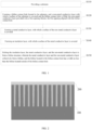
Fig. 1 is a flowchart of a method of manufacturing a semiconductor structure according to an embodiment of the present application; and -
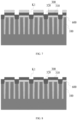
Fig. 2 to Fig. 12 each is a structural schematic diagram of a semiconductor structure subjected to each of etching steps according to an embodiment of the present application. - Reference numerals: substrate-100, bitline contact hole-200, non-metal conductive layer-300, second sublayer of non-metal conductive material-320a, second sublayer of the non-metal conductive layer-320, first sublayer of non-metal conductive material-310a, first sublayer of the non-metal conductive layer-310, metal conductive layer-400, metal barrier material layer-410, metal material layer-420, insulation layer-500, dielectric layer-600, first hard mask layer-700, first hard mask material layer-710, first organic mask material layer-720, second hard mask layer-800, second organic mask material layer-810, second hard mask material layer-820, third hard mask material layer-830, first opening-K1, second opening-K2, bitline structure-900.
- The detailed description of the present application is given below in combination with drawings for the purpose of making the above objectives, features, and advantages of the present application more obvious and understandable. Many details are elaborated in the description below so as to fully comprehend the present application. However, the present application may be implemented in a number of other ways which are different from those described herein. The person skilled in the art can make similar improvements without departing from the connotation of the present application. Therefore, the present application is not limited to the specific implementations disclosed below.
- Referring to
Fig. 1 , a method of manufacturing a semiconductor structure according to an embodiment of the present application is provided. The method includes the following steps: - Step S110: providing a
substrate 100; - Step S120: forming a
bitline contact hole 200 located in thesubstrate 100, and a non-metalconductive layer 300 with which a surface of thesubstrate 100 is covered and thebitline contact hole 200 is filled, the non-metalconductive layer 300 provided with a first opening K1 therein, the first opening K1 aligned with thebitline contact hole 200; - Step S130: forming a metal
conductive layer 400, with which a surface of the non-metalconductive layer 300 is covered; - Step S 140: forming an
insulation layer 500, with which a surface of the metalconductive layer 400 is covered; and - Step S150: etching the
insulation layer 500, the metalconductive layer 400, and the non-metalconductive layer 300 to form abitline structure 900; wherein the metal conductive layer and the non-metal conductive layer collectively form a bitline, and the bitline located in the bitline contact hole has a width no less than the bitline located outside of the bitline contact hole. - It can be understood that in the present application, with formation of the non-metal
conductive layer 300 having the first opening K1, a duration of etching the metalconductive layer 400 located outside of thebitline contact hole 200 is increased in the course of forming thebitline structure 900 by an etching process, such that the metalconductive layer 400 located outside of thebitline contact hole 200 has a width less than or equal to a bottom of the metalconductive layer 400 located in thebitline contact hole 200, so as to increase the area of a node contact window and a bitline separately contacting an active region, reduce a node contact resistance and a bitline contact resistance, and improve a quality of the semiconductor structure. - In this embodiment, the
substrate 100 includes a silicon substrate, an epitaxial silicon substrate, a silicon-germanium substrate, a silicon carbide substrate or a silicon-coated insulation substrate, but not limited thereto. The person skilled in the art may select a type of thesubstrate 100 based on the semiconductor structure formed on thesubstrate 100. Therefore, the type of thesubstrate 100 should not limit the protection scope of the present application. In this embodiment, thesubstrate 100 is a P-typecrystalline silicon substrate 100. - The
substrate 100 includes a base and a shallow trench structure formed in the base. The shallow trench structure defines a plurality of active regions in a parallel staggered arrangement, and is filled with insulation material to form a shallow trench isolation structure. Thesubstrate 100 also includes a wordline structure, which is an embedded wordline structure; an extending direction of the embedded wordline structure intersects with an extending direction of thebitline structure 900. In addition, the wordline structure may also be formed on the surface of the base. - In one of the embodiments, in the
bitline structure 900, the bitline located in thebitline contact hole 200 has a width greater than the bitline outside of thebitline contact hole 200. - The width of the bitline is a width of a projection of the bitline along a direction perpendicular to the substrate. In this embodiment, the bottom of the metal
conductive layer 400 located in thebitline contact hole 200 has a width of d1, the metalconductive layer 400 located outside of thebitline contact hole 200 has a width of d2, wherein d1>d2. In the case where the width of d1 has a greater value, a width of the non-metalconductive layer 300 located below is increased therewith; thus, an overall width of the bitline located in thebitline contact hole 200 is increased (including the metal conductive layer and the non-metal conductive layer), and the contact area between the non-metal conductive layer and the active region is increased and thus, the contact resistance between them is decreased. Besides, by thinning the metalconductive layer 400 located outside of thebitline contact hole 200, the width of the non-metalconductive layer 300 located below is reduced, the contact area between the node contact window and the active region is increased, and the contact resistance between the contact window and the active region is decreased. - In one of the embodiments, the method of manufacturing the semiconductor structure further includes:
adielectric layer 600, with which the surface of thesubstrate 100 is covered, is formed prior to forming thebitline contact hole 200 and the non-metalconductive layer 300. - Referring to
Fig. 2 , dielectric material is deposited on the surface of thesubstrate 100 by a deposition process, so as to form thedielectric layer 600, with which the surface of thesubstrate 100 is covered. The dielectric material may include any one or combination of silicon oxide, silicon oxynitride, amorphous silicon, amorphous carbon or other dielectric material. The deposition process may include chemical vapor deposition, CVD, low pressure CVD, LPCVD, plasma enhanced CVD, PECVD, an atomic layer deposition, ALD, and plasma enhanced ALD, PEALD. - After the
dielectric layer 600 is formed, a next step is generally to manufacture thebitline contact hole 200, while the step of forming the bitline contact hole and the step of manufacturing the non-metal conductive layer are combined in the present application for the purposes of saving a manufacturing cost and simplifying a manufacturing process. In one of the embodiments, the step of forming thebitline contact hole 200 and the non-metalconductive layer 300 includes: - forming a first sublayer of non-metal
conductive material 310a on thesubstrate 100; - etching the first sublayer of non-metal
conductive material 310a and thesubstrate 100 to form thebitline contact hole 200, the retained first sublayer of non-metalconductive material 310a serving as afirst sublayer 310 of the non-metal conductive layer; and - forming a
second sublayer 320 of the non-metal conductive layer, with which thebitline contact hole 200 is filled and a top of which is lower than a top of thefirst sublayer 310 of the non-metal conductive layer, the first andsecond sublayers conductive layer 300. - Referring to
Fig. 3 , the procedure of forming thebitline contact hole 200 and the non-metalconductive layer 300 according to this embodiment includes the following steps. - Step 1: non-metal conductive material, such as polycrystalline silicon, noncrystalline silicon or other non-metal conductive materials with or without silicon, is deposited by the deposition process to form a first sublayer of non-metal conductive material 300a; referring to
Fig. 3 , the surface of thesubstrate 100 is entirely covered by the first sublayer of non-metalconductive material 310a. - Step 2: etching the first sublayer of non-metal
conductive material 310a and thesubstrate 100 to form thebitline contact hole 200, the retained first sublayer of non-metalconductive material 310a serving as afirst sublayer 310 of the non-metal conductive layer. Referring toFigs. 4 and5 , in one of the embodiments, the step of etching the first sublayer of non-metalconductive material 310a and thesubstrate 100 to form thebitline contact hole 200 includes: forming a first hard mask layer on the first sublayer of non-metalconductive material 310a, the first hard mask layer having a first graphical target pattern, the first graphical target pattern defining thebitline contact hole 200; etching, based on the first hard mask layer, the first sublayer of non-metalconductive material 310a and thesubstrate 100 to form thebitline contact hole 200. - In this embodiment, the procedure of forming the first
hard mask layer 700 includes: sequentially forming a first hardmask material layer 710 and a first organicmask material layer 720 on a surface of the first sublayer of non-metalconductive material 310a, wherein the first hardmask material layer 710 is formed using silicon oxide or other insulation materials, the first organicmask material layer 720 is formed using organic materials containing silicon; forming the first hard mask layer 70 consisting of the first hardmask material layer 710 and the first organicmask material layer 720; then, coating a layer of photoresist on the first organicmask material layer 720 to form a first photoresist layer (not shown), and patterning the first photoresist layer by a photolithography process, the patterned first photoresist layer having a first graphical target pattern defining thebitline structure 900; finally, with the first photoresist layer serving as a mask, etching the first hardmask material layer 710 and the first organicmask material layer 720 to transfer the first graphical target pattern to the firsthard mask layer 700. In addition, after thebitline structure 900 is formed, removing the first organicmask material layer 720 and the first photoresist layer, and retaining only the first hard mask material layer as the first hard mask layer. - Step 3: forming the
second sublayer 320 of the non-metal conductive layer. In one of the embodiments, the step of forming thesecond sublayer 320 of the non-metal conductive layer includes: - forming a second sublayer of non-metal
conductive material 320a, with which thebitline contact hole 200 is filled and the surface of the firsthard mask layer 700 is covered; - etching the second sublayer of non-metal
conductive material 320a based on the firsthard mask layer 700 until a top of the first sublayer of non-metalconductive material 310a is higher than a top of the second sublayer of non-metalconductive material 320a, and a height difference between the top of the first sublayer of non-metalconductive material 310a and the top of the second sublayer of non-metalconductive material 320a equals to a preset value, the retained second sublayer of non-metalconductive material 320a serving as thesecond sublayer 320 of the non-metal conductive layer. - In this embodiment, the procedure of forming the
second sublayer 320 of the non-metal conductive layer is as follows. - 1) Firstly, referring to
Fig. 6 , non-metal conductive material, such as polycrystalline silicon, noncrystalline silicon or other non-metal conductive materials with or without silicon, is deposited by the deposition process to form the first sublayer of non-metalconductive material 320a, with which the surface of the first hardmask material layer 710 is entirely covered and thebitline contact hole 200 is filled. In this embodiment, both of the first sublayer of non-metalconductive material 310a and the second sublayer of non-metalconductive material 320a are made of polycrystalline silicon material for ease of material management and reduction in manufacturing cost. - 2) Secondly, referring to
Fig. 7 , etching the second sublayer of non-metalconductive material 320a based on the first hardmask material layer 710 until the second sublayer of non-metalconductive material 320a located on an upper surface of the first hardmask material layer 710 is completely removed, a top of the first sublayer of non-metalconductive material 310a is higher than a top of the second sublayer of non-metalconductive material 320a, and a height difference between the top of the first sublayer of non-metalconductive material 310a and the top of the second sublayer ofnon-metal material 320a equals to a preset value, the retained second sublayer of non-metalconductive material 320a serving as thesecond sublayer 320 of the non-metal conductive layer. The first andsecond sub-layers bitline contact hole 200. Moreover, since the same hard mask layer is used, namely using the first hardmask material layer 710 as a mask for the etching process, so as to form thebitline contact hole 200 and the second sublayer of non-metalconductive material 320a, in this embodiment, the first opening K1 has a width equal to the bitline contact hole. And, the procedure of forming thebitline contact hole 200 is combined with the procedure of forming the non-metalconductive layer 300, and the same hard mask layer is used as the mask for the etch, which are beneficial to simplify the processes and reduce the manufacturing cost. In some of other embodiments, thebitline contact hole 200 and the non-metalconductive layer 300 may also be formed step by step. For example, the bitline contact hole is formed first, and then the noncrystalline silicon material layer, with which the bitline contact hole is filled and the surface of the substrate is covered, is formed and back-etched to form the first opening K1. - Step 4: removing the first hard
mask material layer 710 by a chemical-mechanical polishing process; please refer toFig. 8 . - In some of other embodiments, the
second sublayer 320 of the non-metal conductive layer may also be formed using non-metal conductive materials with different etching ratios, the procedure of which includes the following steps. - Step 1: first removing the first hard
mask material layer 710 by the chemical-mechanical polishing process. - Step 2: depositing non-metal conductive material to form the second sublayer of non-metal
conductive material 320a, with which thefirst sublayer 310 of the non-metal conductive layer is covered and thebitline contact hole 200 is filled. Besides, the first sublayer of non-metalconductive material 310a is of different material from the second sublayer of non-metalconductive material 320a. For example, the first sublayer of non-metalconductive material 320a is made of polycrystalline silicon, and the second sublayer of non-metalconductive material 320a is made of semiconductor oxide, wherein the semiconductor oxide has an etching rate greater than the polycrystalline silicon (e.g., under a certain etching condition, a ratio of the etching rate of the semiconductor oxide to the etching rate of the polycrystalline silicon is greater than 10). - Step 3: etching the first sublayer of non-metal
conductive material 310a and the second sublayer of non-metalconductive material 320a based on their etching ratio, until the top of the first sublayer of non-metalconductive material 310a is higher than the top of the second sublayer of non-metalconductive material 320a, and a height difference between the top of the first sublayer of non-metalconductive material 310a and the top of the second sublayer of non-metalconductive material 320a equals to a preset value to form the first opening K1. - Referring to
Fig. 9 , after the bitline contact hole and the non-metal conductive layer are formed, the metal conductive layer is required to be manufactured in a next step. In one of the embodiments, the steps of forming the metalconductive layer 400 include: - forming a metal
barrier material layer 410, with which the surface of the non-metalconductive layer 300 is covered; and - forming a
metal material layer 420, with which a surface of the metalbarrier material layer 410 is covered. - In this embodiment, the metal
conductive layer 400 is of a laminated construction, including the metalbarrier material layer 410 and themetal material layer 420 disposed sequentially from bottom to top. The metalbarrier material layer 410 and themetal material layer 420 may be formed by a stack of any one or combination of titanium nitride, titanium, tungsten silicide or a tungsten nitride and tungsten; wherein the metalbarrier material layer 410 is formed using any one or combination of titanium nitride, titanium, tungsten silicide, tungsten nitride or tungsten silicon nitride. Besides, the metalconductive layer 400 may also be formed using other metals, metal nitride, metal silicide, and metal silicon nitride. - In one of the embodiments, the metal
conductive layer 400 is formed by an atomic layer deposition technology. It can be understood that the atomic layer deposition technology is a method of plating a substance in a form of a single atom membrane layer by layer on a surface of the base. Compared with an ordinary chemical deposition technology, the metalconductive layer 400 formed by the atomic layer deposition technology has a highly uniform membrane thickness and a consistency on its surface, and can directly form the second opening K2 located above the first opening K1. In some of other embodiments, themetal material layer 420 may be first formed by other chemical deposition processes, and then etched by back-etching to form the metalconductive layer 400 having the second opening K2. Additionally, the second opening K2 may not be formed. In this embodiment, in the case where the atomic layer deposition technology is used to form the metal conductive layer, since the metalbarrier material layer 410 and themetal material layer 420 are also formed on a side wall of the first opening K1, the second opening K2 has a width slightly less than the first opening K1. - In one of the embodiments, the procedure of forming the
insulation layer 500, with which the surface of the metalconductive layer 400 is covered, mainly includes: depositing silicon nitride, silicon oxynitride, silicon carbide or other suitable insulation material to form theinsulation layer 500, with which the surface of themetal material layer 420 is covered and the second opening K2 is filled. Moreover, in order to reduce a probability of electric leakage between the bitline and the capacitor contact line, a thickness of theinsulation layer 500 is normally increased to mitigate such a phenomenon. Therefore, in this embodiment, theinsulation layer 500 has a thickness much greater than the metalconductive layer 400 and/or the non-metalconductive layer 300. - In one of the embodiments, the step of etching the
insulation layer 500, the metalconductive layer 400, and the non-metalconductive layer 300 to form thebitline structure 900 includes: - forming a second
hard mask layer 800 on theinsulation layer 500, the secondhard mask layer 800 having a second graphical target pattern, the second graphical target pattern defining thebitline structure 900; - with the metal
conductive layer 400 serving as an etch stop layer, using the secondhard mask layer 800 as a mask to etch theinsulation layer 500 to transfer the second graphical target pattern to theinsulation layer 500; - removing the second
hard mask layer 800; and - with the
insulation layer 500 serving as a mask, etching the metalconductive layer 400 and the non-metalconductive layer 300 to form thebitline structure 900. - In this embodiment, the main procedure of etching the
insulation layer 500, the metalconductive layer 400, and the non-metalconductive layer 300 to form thebitline structure 900 is as follows. - 1) Referring to
Fig. 10 , the secondhard mask layer 800 is formed. In this embodiment, the secondhard mask layer 800 is formed by a self-aligning dual imaging technology. The forming procedure mainly includes: firstly, sequentially depositing an amorphous carbon material, a silicon oxynitride material, and an oxide material on the surface of theinsulation layer 500 to form a second organicmask material layer 810, a second hardmask material layer 820, and a sacrificial material layer (not shown); coating a layer of photoresist on the sacrificial material layer to form a second photoresist layer, and transferring a pattern of a mask to the sacrificial material layer by using the photolithography technique. Secondly, the atomic layer deposition technology is used to deposit hard mask material on a surface of the sacrificial material layer to form a third hard mask material layer; back-etching the third hard mask material layer and retaining the third hardmask material layer 830 located on a side wall of the sacrificial material layer as the second graphical target pattern, so as to define thebitline structure 900. Then, the second graphical target pattern is sequentially transferred to the second hardmask material layer 820 and the second organicmask material layer 810. Finally, the third hardmask material layer 830 is removed to form the secondhard mask layer 800 including the second hardmask material layer 820 and the second organicmask material layer 810. - 2) Referring to
Fig. 11 , with the metalconductive layer 400 serving as an etch stop layer, using the secondhard mask layer 800 as a mask to etch theinsulation layer 500 to transfer the second graphical target pattern to theinsulation layer 500. In this embodiment, a fluorine-containing etching is used to etch theinsulation layer 500, fluorine-containing etching gases include one or more of octafluorocyclobutanne, octafluorocyclopentene, and hexafuorobutadiene. After theinsulation layer 500 is etched, the secondhard mask layer 800 is removed. - 3) Referring to
Fig. 12 , with theinsulation layer 500 serving as a mask, etching the metalconductive layer 400 and the non-metalconductive layer 300 to form thebitline structure 900. In this embodiment, the procedure of etching the metalconductive layer 400 and the non-metalconductive layer 300 is mainly as follows. - Firstly, with the metal
barrier material layer 410 serving as an etching stop layer, theinsulation layer 500 is used as a mask to etch themetal material layer 420 to transfer the second graphical target pattern to themetal material layer 420; in this embodiment, themetal material layer 420 is made of tungsten, and thus, an etching gas containing silicon hexafluoride may be used to etch themetal material layer 420 in this step. - Secondly, with the non-metal
conductive layer 300 serving as an etching stop layer, theinsulation layer 500 is used as the mask to etch the metalbarrier material layer 410 to transfer the second graphical target pattern to the metalbarrier material layer 410; in this embodiment, silicon nitride is used to manufacture the metalbarrier material layer 410. - Then, the
insulation layer 500 is used as the mask to etch the non-metalconductive layer 300 to transfer the second graphical target pattern to the non-metalconductive layer 300. In this embodiment, the polycrystalline silicon material is used to form the non-metalconductive layer 300, and chlorine is used to etch the non-metalconductive layer 300. Since it is easier for micromolecular chlorine to enter thebitline contact hole 200, the duration of etching the non-metalconductive layer 300 may be shortened, ensuring that the etched non-metalconductive layer 300 has a good shape and a large width. The non-metalconductive layer 300 is of a cross-section shape of trapezoid after being etched. The non-metalconductive layer 300 of this shape may provide a good support to the metal conductive layer and the insulation layer located above it, reducing a collapsing risk for thebitline structure 900. - An embodiment of the present application further provides a semiconductor structure formed using the manufacturing method according to any of the embodiments described above. With continued reference to
Fig. 12 , the semiconductor structure includes asubstrate 100 and abitline structure 900. - The
substrate 100 has a plurality of bitline contact holes 200. - The
bitline structure 900 includes a non-metalconductive layer 300, a metalconductive layer 400, and aninsulation layer 500 disposed from bottom to top as a stack, wherein the non-metalconductive layer 300 is sequentially and alternately located on a surface of thesemiconductor substrate 100 and a bottom of thebitline contact hole 200; wherein the metalconductive layer 400 and the non-metalconductive layer 300 collectively form a bitline, and the bitline located in the bitline contact hole has a width no less than the bitline located outside of the bitline contact hole. - It can be understood that in this embodiment, the semiconductor structure is manufactured by using the method according to the embodiments described above; with the formation of the non-metal
conductive layer 300 having a first opening K1 and the formation of the metalconductive layer 400 having a second opening K2 during the manufacturing procedure, such that the duration of etching the metalconductive layer 400 located outside of thebitline contact hole 200 is increased in the course of forming thebitline structure 900 by the etching process, and the metalconductive layer 400 located outside of thebitline contact hole 200 has a width less than or equal to the bottom of the metalconductive layer 400 located in thebitline contact hole 200, which is beneficial to increase the area of the node contact window and thebitline structure 900 contacting the active region, reducing the node contact resistance and the bitline contact resistance, and improving the quality of the semiconductor structure. - In this embodiment, the
substrate 100 includes a base and a shallow trench structure formed in the base. The shallow trench structure defines a plurality of active regions in a parallel staggered arrangement, and is filled with insulation material to form a shallow trench isolation structure. Thesubstrate 100 also includes a wordline structure, which is an embedded wordline structure; an extending direction of the embedded wordline structure intersects with an extending direction of thebitline structure 900. In addition, the wordline structure may also be formed on the surface of the base. - In one of the embodiments, in the
bitline structure 900, the bottom of the metalconductive layer 400 located in thebitline contact hole 200 has a width greater than the metalconductive layer 400 located outside of thebitline contact hole 200. - In this embodiment, the bottom of the metal
conductive layer 400 located in thebitline contact hole 200 has a width of d1, the metalconductive layer 400 located outside of thebitline contact hole 200 has a width of d2, wherein d1>d2. In the case where the width of d1 has a greater value, a width of the non-metalconductive layer 300 located below is increased therewith; thus, an overall width of the bitline located in thebitline contact hole 200 is increased, and the contact area between the bitline and the active region is increased and thus, the contact resistance between them is decreased. Besides, by thinning the metalconductive layer 400 located outside of thebitline contact hole 200, the width of the non-metalconductive layer 300 located below is reduced, the contact area between the node contact window and the active region is increased, reducing the node contact resistance. - In one of the embodiments, the semiconductor structure further includes a
dielectric layer 600 located between the surface of thesubstrate 100 and the non-metalconductive layer 300. In this embodiment, the wordline structure and the bitline structure is isolated by thedielectric layer 600. - Technical features of the embodiments described above may be arbitrarily combined, but not all of the potential combinations are described so as to make the description concise. However, all of the combinations of these technical features should be considered as the scope recited in the specification as long as they have no conflict therein.
- The embodiments described above merely show several implementations of the present application. The descriptions thereof are detailed, but should not be interpreted as limiting the scope of the patent application. It should be noted that the person skilled in the art could further make several variations and improvements without departing the concept of the present application, and these variations and improvements belong to the scope sought for protection in the present application. Therefore, the protection scope of the present patent application shall be subject to the claims.
Claims (15)
- A method of manufacturing a semiconductor structure, comprising:providing a substrate;forming a bitline contact hole located in the substrate, and forming a non-metal conductive layer to cover a surface of the substrate and fill the bitline contact hole, the non-metal conductive layer having a first opening formed therein, the first opening aligned with the bitline contact hole;forming a metal conductive layer to cover a surface of the non-metal conductive layer;forming an insulation layer to cover a surface of the metal conductive layer; andetching the insulation layer, the metal conductive layer, and the non-metal conductive layer to form a bitline structure;wherein the metal conductive layer and the non-metal conductive layer collectively form a bitline, and the bitline located in the bitline contact hole has a width not less than that of the bitline located outside of the bitline contact hole.
- The method of manufacturing the semiconductor structure according to claim 1, wherein in the bitline structure, the bitline located in the bitline contact hole has a width greater than that of the bitline outside of the bitline contact hole.
- The method of manufacturing the semiconductor structure according to claim 1, wherein forming the bitline contact hole and the non-metal conductive layer comprises:forming a first sublayer of non-metal conductive material on the substrate;etching the first sublayer of non-metal conductive material and the substrate to form the bitline contact hole, the retained first sublayer of non-metal conductive material serving as a first sublayer of the non-metal conductive layer; andforming a second sublayer of the non-metal conductive layer to cover the bitline contact hole, and a top of the second sublayer of the non-metal conductive layer is lower than a top of the first sublayer of the non-metal conductive layer, the first and second sub-layers of the non-metal conductive layer collectively forming the non-metal conductive layer.
- The method of manufacturing the semiconductor structure according to claim 3, wherein etching the first sublayer of non-metal conductive material and the substrate to form the bitline contact hole comprises:forming a first hard mask layer on the first sublayer of non-metal conductive material, the first hard mask layer having a first graphical target pattern, the first graphical target pattern defining the bitline contact hole; andetching, based on the first hard mask layer, the first sublayer of non-metal conductive material and the substrate to form the bitline contact hole.
- The method of manufacturing the semiconductor structure according to claim 4, wherein forming the second sublayer of the non-metal conductive layer comprises:forming a second sublayer of non-metal conductive material to fill the bitline contact hole and to cover a surface of the first hard mask layer; andetching the second sublayer of non-metal conductive material based on the first hard mask layer until a height difference between a top of the first sublayer of non-metal conductive material and a top of the second sublayer of non-metal conductive material equals to a preset value, the retained second sublayer of non-metal conductive material serving as the second sublayer of the non-metal conductive layer.
- The method of manufacturing the semiconductor structure according to claim 1, wherein an atomic layer deposition technology is used to form the metal conductive layer.
- The method of manufacturing the semiconductor structure according to claim 1, wherein forming the metal conductive layer comprises:forming a metal barrier material layer to cover the surface of the non-metal conductive layer; andforming a metal material layer to cover a surface of the metal barrier material layer.
- The method of manufacturing the semiconductor structure according to claim 1, wherein etching the insulation layer, the metal conductive layer, and the non-metal conductive layer to form the bitline structure comprises:forming a second hard mask layer on the insulation layer, the second hard mask layer having a second graphical target pattern, the second graphical target pattern defining the bitline structure;with the metal conductive layer serving as an etching stop layer, using the second hard mask layer as a mask to etch the insulation layer to transfer the second graphical target pattern to the insulation layer;removing the second hard mask layer; andwith the insulation layer serving as a mask, etching the metal conductive layer and the non-metal conductive layer to form the bitline structure.
- The method of manufacturing the semiconductor structure according to claim 8, wherein using the insulation layer as the mask to etch the metal conductive layer and the non-metal conductive layer comprises:with a metal barrier material layer serving as an etching stop layer, using the insulation layer as a mask to etch metal material to transfer the second graphical target pattern to the metal conductive layer;with the non-metal conductive layer serving as an etching stop layer, using the insulation layer as the mask to etch the metal barrier material layer to transfer the second graphical target pattern to the metal barrier material layer; andusing the insulation layer as the mask to etch the non-metal conductive layer to transfer the second graphical target pattern to the non-metal conductive layer.
- The method of manufacturing the semiconductor structure according to claim 1, wherein a polycrystalline material is used to manufacture a non-metal conductive material layer.
- The method of manufacturing the semiconductor structure according to claim 10, wherein an etching gas containing Cl2 is used to etch the non-metal conductive layer.
- The method of manufacturing the semiconductor structure according to claim 1, wherein the method further comprises:
before the bitline contact hole and the non-metal conductive layer are formed, forming a dielectric layer to cover the surface of the substrate. - A semiconductor structure, comprising:a substrate with a plurality of bitline contact holes; anda bitline structure including a non-metal conductive layer, a metal conductive layer, and an insulation layer disposed from bottom to top as a stack, wherein the non-metal conductive layer is sequentially located on a surface of the substrate and a bottom of a given one of the plurality of bitline contact holes;wherein the metal conductive layer and the non-metal conductive layer collectively form a bitline, and the bitline located in the bitline contact hole has a width not less than that of the bitline located outside of the bitline contact hole.
- The semiconductor structure according to claim 13, wherein in the bitline structure, the bitline located in the bitline contact hole has a width greater than that of the bitline outside of the bitline contact hole.
- The semiconductor structure according to claim 13, further comprising a dielectric layer located between the surface of the substrate and the non-metal conductive layer.
Applications Claiming Priority (2)
| Application Number | Priority Date | Filing Date | Title |
|---|---|---|---|
| CN202010684751.5A CN113948473B (en) | 2020-07-16 | 2020-07-16 | Semiconductor structure and method for manufacturing the same |
| PCT/CN2021/100787 WO2022012263A1 (en) | 2020-07-16 | 2021-06-18 | Semiconductor structure and manufacturing method therefor |
Publications (2)
| Publication Number | Publication Date |
|---|---|
| EP4163975A1 true EP4163975A1 (en) | 2023-04-12 |
| EP4163975A4 EP4163975A4 (en) | 2023-12-06 |
Family
ID=79292821
Family Applications (1)
| Application Number | Title | Priority Date | Filing Date |
|---|---|---|---|
| EP21843091.6A Pending EP4163975A4 (en) | 2020-07-16 | 2021-06-18 | SEMICONDUCTOR STRUCTURE AND ITS MANUFACTURING METHOD |
Country Status (2)
| Country | Link |
|---|---|
| US (1) | US11930635B2 (en) |
| EP (1) | EP4163975A4 (en) |
Families Citing this family (1)
| Publication number | Priority date | Publication date | Assignee | Title |
|---|---|---|---|---|
| CN119155991B (en) * | 2023-06-08 | 2025-09-26 | 长鑫存储技术有限公司 | Semiconductor structure and preparation method thereof |
Family Cites Families (9)
| Publication number | Priority date | Publication date | Assignee | Title |
|---|---|---|---|---|
| KR101129922B1 (en) * | 2010-07-15 | 2012-03-23 | 주식회사 하이닉스반도체 | Semiconductor device and method for forming the same |
| KR101994820B1 (en) * | 2012-07-26 | 2019-07-02 | 에스케이하이닉스 주식회사 | Semiconductor with stacked silicon containing layer and metal containing layer and method for fabricating the same |
| KR102235611B1 (en) * | 2014-06-13 | 2021-04-02 | 삼성전자주식회사 | Method of forming patterns and method of manufacturing integrated circuit device using the same |
| KR102283813B1 (en) | 2014-12-04 | 2021-08-03 | 삼성전자주식회사 | Semiconductor device and method for manufacturing the same |
| CN108257958A (en) | 2016-12-29 | 2018-07-06 | 联华电子股份有限公司 | Bit line grid structure of dynamic random access memory and forming method |
| CN110581103B (en) * | 2018-06-07 | 2022-04-12 | 联华电子股份有限公司 | Semiconductor device and method of making the same |
| US10651177B1 (en) * | 2018-11-07 | 2020-05-12 | Nanya Technology Corporation | Semiconductor device and method of forming the same |
| KR102691496B1 (en) * | 2019-07-29 | 2024-08-01 | 삼성전자주식회사 | Semiconductor device |
| CN121149124A (en) | 2019-09-30 | 2025-12-16 | 福建省晋华集成电路有限公司 | Semiconductor storage devices |
-
2021
- 2021-06-18 EP EP21843091.6A patent/EP4163975A4/en active Pending
- 2021-08-11 US US17/399,062 patent/US11930635B2/en active Active
Also Published As
| Publication number | Publication date |
|---|---|
| US20220020751A1 (en) | 2022-01-20 |
| EP4163975A4 (en) | 2023-12-06 |
| US11930635B2 (en) | 2024-03-12 |
Similar Documents
| Publication | Publication Date | Title |
|---|---|---|
| KR100716641B1 (en) | Cylindrical Capacitor Manufacturing Method Using Amorphous Carbon Layer | |
| KR100799152B1 (en) | Manufacturing method of cylindrical capacitor which prevents storage node from falling | |
| US10014316B2 (en) | Three-dimensional memory device with leakage reducing support pillar structures and method of making thereof | |
| US6667209B2 (en) | Methods for forming semiconductor device capacitors that include an adhesive spacer that ensures stable operation | |
| US9530785B1 (en) | Three-dimensional memory devices having a single layer channel and methods of making thereof | |
| US6653186B2 (en) | Methods of fabrication integrated circuit capacitors having a dielectric layer between a u-shaped lower electrode and a support layer | |
| CN111710682B (en) | Three-dimensional memory and preparation method thereof | |
| US20010034100A1 (en) | Methods of forming self-aligned contact pads on electrically conductive lines | |
| JP5294182B2 (en) | Method for forming capacitor storage node of semiconductor device | |
| US11930635B2 (en) | Semiconductor structure and method of manufacturing same | |
| CN113948473B (en) | Semiconductor structure and method for manufacturing the same | |
| EP3971990A1 (en) | Semiconductor structure and method for manufacturing same | |
| US12349352B2 (en) | Three-dimensional memory device including a dummy word line with tapered corner and method of making the same | |
| CN114078773A (en) | Capacitor structure, manufacturing method thereof and memory | |
| CN113948474B (en) | Semiconductor structure and method for manufacturing the same | |
| US5480824A (en) | Semiconductor memory cell capacitor and fabrication method thereof | |
| KR20110078020A (en) | Method of manufacturing a semiconductor device having a filler charge storage electrode | |
| US12310020B2 (en) | Three-dimensional memory device including a dummy word line with tapered corner and method of making the same | |
| US12520476B2 (en) | Semiconductor device and method of manufacturing the same | |
| KR100677769B1 (en) | Capacitor and manufacturing method thereof | |
| US6190956B1 (en) | Forming a capacitor structure of a semiconductor | |
| KR20120052504A (en) | Capacitor with double cylinder type storage node and method for manufacturing capacitor | |
| KR100680962B1 (en) | Capacitor Formation Method of Semiconductor Device | |
| KR100587032B1 (en) | Manufacturing Method of Semiconductor Memory Device | |
| CN117355130A (en) | Semiconductor structure and method of forming same, memory |
Legal Events
| Date | Code | Title | Description |
|---|---|---|---|
| STAA | Information on the status of an ep patent application or granted ep patent |
Free format text: STATUS: THE INTERNATIONAL PUBLICATION HAS BEEN MADE |
|
| PUAI | Public reference made under article 153(3) epc to a published international application that has entered the european phase |
Free format text: ORIGINAL CODE: 0009012 |
|
| STAA | Information on the status of an ep patent application or granted ep patent |
Free format text: STATUS: REQUEST FOR EXAMINATION WAS MADE |
|
| 17P | Request for examination filed |
Effective date: 20230106 |
|
| AK | Designated contracting states |
Kind code of ref document: A1 Designated state(s): AL AT BE BG CH CY CZ DE DK EE ES FI FR GB GR HR HU IE IS IT LI LT LU LV MC MK MT NL NO PL PT RO RS SE SI SK SM TR |
|
| DAV | Request for validation of the european patent (deleted) | ||
| DAX | Request for extension of the european patent (deleted) | ||
| REG | Reference to a national code |
Ref country code: DE Ref legal event code: R079 Free format text: PREVIOUS MAIN CLASS: H01L0027108000 Ipc: H10B0012000000 |
|
| A4 | Supplementary search report drawn up and despatched |
Effective date: 20231107 |
|
| RIC1 | Information provided on ipc code assigned before grant |
Ipc: H10B 12/00 20230101AFI20231031BHEP |
|
| GRAP | Despatch of communication of intention to grant a patent |
Free format text: ORIGINAL CODE: EPIDOSNIGR1 |
|
| STAA | Information on the status of an ep patent application or granted ep patent |
Free format text: STATUS: GRANT OF PATENT IS INTENDED |
|
| INTG | Intention to grant announced |
Effective date: 20260316 |
|
| P01 | Opt-out of the competence of the unified patent court (upc) registered |
Free format text: CASE NUMBER: UPC_APP_0011915_4163975/2026 Effective date: 20260403 |