EP4163955A1 - Sic semiconductor element manufacturing method and sic semiconductor element - Google Patents
Sic semiconductor element manufacturing method and sic semiconductor element Download PDFInfo
- Publication number
- EP4163955A1 EP4163955A1 EP21817045.4A EP21817045A EP4163955A1 EP 4163955 A1 EP4163955 A1 EP 4163955A1 EP 21817045 A EP21817045 A EP 21817045A EP 4163955 A1 EP4163955 A1 EP 4163955A1
- Authority
- EP
- European Patent Office
- Prior art keywords
- sic substrate
- film
- sio
- sic
- interface
- Prior art date
- Legal status (The legal status is an assumption and is not a legal conclusion. Google has not performed a legal analysis and makes no representation as to the accuracy of the status listed.)
- Granted
Links
Images







Classifications
-
- H—ELECTRICITY
- H10—SEMICONDUCTOR DEVICES; ELECTRIC SOLID-STATE DEVICES NOT OTHERWISE PROVIDED FOR
- H10D—INORGANIC ELECTRIC SEMICONDUCTOR DEVICES
- H10D62/00—Semiconductor bodies, or regions thereof, of devices having potential barriers
- H10D62/80—Semiconductor bodies, or regions thereof, of devices having potential barriers characterised by the materials
- H10D62/83—Semiconductor bodies, or regions thereof, of devices having potential barriers characterised by the materials being Group IV materials, e.g. B-doped Si or undoped Ge
- H10D62/832—Semiconductor bodies, or regions thereof, of devices having potential barriers characterised by the materials being Group IV materials, e.g. B-doped Si or undoped Ge being Group IV materials comprising two or more elements, e.g. SiGe
- H10D62/8325—Silicon carbide
-
- H—ELECTRICITY
- H10—SEMICONDUCTOR DEVICES; ELECTRIC SOLID-STATE DEVICES NOT OTHERWISE PROVIDED FOR
- H10D—INORGANIC ELECTRIC SEMICONDUCTOR DEVICES
- H10D12/00—Bipolar devices controlled by the field effect, e.g. insulated-gate bipolar transistors [IGBT]
- H10D12/01—Manufacture or treatment
- H10D12/031—Manufacture or treatment of IGBTs
-
- H—ELECTRICITY
- H10—SEMICONDUCTOR DEVICES; ELECTRIC SOLID-STATE DEVICES NOT OTHERWISE PROVIDED FOR
- H10D—INORGANIC ELECTRIC SEMICONDUCTOR DEVICES
- H10D64/00—Electrodes of devices having potential barriers
- H10D64/01—Manufacture or treatment
- H10D64/013—Manufacture or treatment of electrodes having a conductor capacitively coupled to a semiconductor by an insulator
- H10D64/01366—Manufacture or treatment of electrodes having a conductor capacitively coupled to a semiconductor by an insulator the semiconductor being silicon carbide
-
- H—ELECTRICITY
- H10—SEMICONDUCTOR DEVICES; ELECTRIC SOLID-STATE DEVICES NOT OTHERWISE PROVIDED FOR
- H10D—INORGANIC ELECTRIC SEMICONDUCTOR DEVICES
- H10D64/00—Electrodes of devices having potential barriers
- H10D64/60—Electrodes characterised by their materials
- H10D64/66—Electrodes having a conductor capacitively coupled to a semiconductor by an insulator, e.g. MIS electrodes
- H10D64/68—Electrodes having a conductor capacitively coupled to a semiconductor by an insulator, e.g. MIS electrodes characterised by the insulator, e.g. by the gate insulator
- H10D64/693—Electrodes having a conductor capacitively coupled to a semiconductor by an insulator, e.g. MIS electrodes characterised by the insulator, e.g. by the gate insulator the insulator comprising nitrogen, e.g. nitrides, oxynitrides or nitrogen-doped materials
-
- H—ELECTRICITY
- H10—SEMICONDUCTOR DEVICES; ELECTRIC SOLID-STATE DEVICES NOT OTHERWISE PROVIDED FOR
- H10P—GENERIC PROCESSES OR APPARATUS FOR THE MANUFACTURE OR TREATMENT OF DEVICES COVERED BY CLASS H10
- H10P14/00—Formation of materials, e.g. in the shape of layers or pillars
- H10P14/60—Formation of materials, e.g. in the shape of layers or pillars of insulating materials
- H10P14/63—Formation of materials, e.g. in the shape of layers or pillars of insulating materials characterised by the formation processes
- H10P14/6302—Non-deposition formation processes
- H10P14/6304—Formation by oxidation, e.g. oxidation of the substrate
- H10P14/6306—Formation by oxidation, e.g. oxidation of the substrate of the semiconductor materials
- H10P14/6308—Formation by oxidation, e.g. oxidation of the substrate of the semiconductor materials of Group IV semiconductors
-
- H—ELECTRICITY
- H10—SEMICONDUCTOR DEVICES; ELECTRIC SOLID-STATE DEVICES NOT OTHERWISE PROVIDED FOR
- H10P—GENERIC PROCESSES OR APPARATUS FOR THE MANUFACTURE OR TREATMENT OF DEVICES COVERED BY CLASS H10
- H10P14/00—Formation of materials, e.g. in the shape of layers or pillars
- H10P14/60—Formation of materials, e.g. in the shape of layers or pillars of insulating materials
- H10P14/63—Formation of materials, e.g. in the shape of layers or pillars of insulating materials characterised by the formation processes
- H10P14/6302—Non-deposition formation processes
- H10P14/6322—Formation by thermal treatments
-
- H—ELECTRICITY
- H10—SEMICONDUCTOR DEVICES; ELECTRIC SOLID-STATE DEVICES NOT OTHERWISE PROVIDED FOR
- H10P—GENERIC PROCESSES OR APPARATUS FOR THE MANUFACTURE OR TREATMENT OF DEVICES COVERED BY CLASS H10
- H10P14/00—Formation of materials, e.g. in the shape of layers or pillars
- H10P14/60—Formation of materials, e.g. in the shape of layers or pillars of insulating materials
- H10P14/63—Formation of materials, e.g. in the shape of layers or pillars of insulating materials characterised by the formation processes
- H10P14/6326—Deposition processes
- H10P14/6328—Deposition from the gas or vapour phase
- H10P14/6334—Deposition from the gas or vapour phase using decomposition or reaction of gaseous or vapour phase compounds, i.e. chemical vapour deposition
-
- H—ELECTRICITY
- H10—SEMICONDUCTOR DEVICES; ELECTRIC SOLID-STATE DEVICES NOT OTHERWISE PROVIDED FOR
- H10P—GENERIC PROCESSES OR APPARATUS FOR THE MANUFACTURE OR TREATMENT OF DEVICES COVERED BY CLASS H10
- H10P14/00—Formation of materials, e.g. in the shape of layers or pillars
- H10P14/60—Formation of materials, e.g. in the shape of layers or pillars of insulating materials
- H10P14/63—Formation of materials, e.g. in the shape of layers or pillars of insulating materials characterised by the formation processes
- H10P14/6326—Deposition processes
- H10P14/6328—Deposition from the gas or vapour phase
- H10P14/6334—Deposition from the gas or vapour phase using decomposition or reaction of gaseous or vapour phase compounds, i.e. chemical vapour deposition
- H10P14/6336—Deposition from the gas or vapour phase using decomposition or reaction of gaseous or vapour phase compounds, i.e. chemical vapour deposition in the presence of a plasma [PECVD]
-
- H—ELECTRICITY
- H10—SEMICONDUCTOR DEVICES; ELECTRIC SOLID-STATE DEVICES NOT OTHERWISE PROVIDED FOR
- H10P—GENERIC PROCESSES OR APPARATUS FOR THE MANUFACTURE OR TREATMENT OF DEVICES COVERED BY CLASS H10
- H10P14/00—Formation of materials, e.g. in the shape of layers or pillars
- H10P14/60—Formation of materials, e.g. in the shape of layers or pillars of insulating materials
- H10P14/65—Formation of materials, e.g. in the shape of layers or pillars of insulating materials characterised by treatments performed before or after the formation of the materials
- H10P14/6502—Formation of materials, e.g. in the shape of layers or pillars of insulating materials characterised by treatments performed before or after the formation of the materials of treatments performed before formation of the materials
- H10P14/6512—Formation of materials, e.g. in the shape of layers or pillars of insulating materials characterised by treatments performed before or after the formation of the materials of treatments performed before formation of the materials by exposure to a gas or vapour
- H10P14/6514—Formation of materials, e.g. in the shape of layers or pillars of insulating materials characterised by treatments performed before or after the formation of the materials of treatments performed before formation of the materials by exposure to a gas or vapour by exposure to a plasma
-
- H—ELECTRICITY
- H10—SEMICONDUCTOR DEVICES; ELECTRIC SOLID-STATE DEVICES NOT OTHERWISE PROVIDED FOR
- H10P—GENERIC PROCESSES OR APPARATUS FOR THE MANUFACTURE OR TREATMENT OF DEVICES COVERED BY CLASS H10
- H10P14/00—Formation of materials, e.g. in the shape of layers or pillars
- H10P14/60—Formation of materials, e.g. in the shape of layers or pillars of insulating materials
- H10P14/65—Formation of materials, e.g. in the shape of layers or pillars of insulating materials characterised by treatments performed before or after the formation of the materials
- H10P14/6516—Formation of materials, e.g. in the shape of layers or pillars of insulating materials characterised by treatments performed before or after the formation of the materials of treatments performed after formation of the materials
- H10P14/6529—Formation of materials, e.g. in the shape of layers or pillars of insulating materials characterised by treatments performed before or after the formation of the materials of treatments performed after formation of the materials by exposure to a gas or vapour
-
- H—ELECTRICITY
- H10—SEMICONDUCTOR DEVICES; ELECTRIC SOLID-STATE DEVICES NOT OTHERWISE PROVIDED FOR
- H10P—GENERIC PROCESSES OR APPARATUS FOR THE MANUFACTURE OR TREATMENT OF DEVICES COVERED BY CLASS H10
- H10P14/00—Formation of materials, e.g. in the shape of layers or pillars
- H10P14/60—Formation of materials, e.g. in the shape of layers or pillars of insulating materials
- H10P14/66—Formation of materials, e.g. in the shape of layers or pillars of insulating materials characterised by the type of materials
- H10P14/668—Formation of materials, e.g. in the shape of layers or pillars of insulating materials characterised by the type of materials the materials being characterised by the deposition precursor materials
- H10P14/6681—Formation of materials, e.g. in the shape of layers or pillars of insulating materials characterised by the type of materials the materials being characterised by the deposition precursor materials the precursor containing a compound comprising Si
- H10P14/6682—Formation of materials, e.g. in the shape of layers or pillars of insulating materials characterised by the type of materials the materials being characterised by the deposition precursor materials the precursor containing a compound comprising Si the compound being a silane, e.g. disilane, methylsilane or chlorosilane
-
- H—ELECTRICITY
- H10—SEMICONDUCTOR DEVICES; ELECTRIC SOLID-STATE DEVICES NOT OTHERWISE PROVIDED FOR
- H10P—GENERIC PROCESSES OR APPARATUS FOR THE MANUFACTURE OR TREATMENT OF DEVICES COVERED BY CLASS H10
- H10P14/00—Formation of materials, e.g. in the shape of layers or pillars
- H10P14/60—Formation of materials, e.g. in the shape of layers or pillars of insulating materials
- H10P14/66—Formation of materials, e.g. in the shape of layers or pillars of insulating materials characterised by the type of materials
- H10P14/668—Formation of materials, e.g. in the shape of layers or pillars of insulating materials characterised by the type of materials the materials being characterised by the deposition precursor materials
- H10P14/6681—Formation of materials, e.g. in the shape of layers or pillars of insulating materials characterised by the type of materials the materials being characterised by the deposition precursor materials the precursor containing a compound comprising Si
- H10P14/6684—Formation of materials, e.g. in the shape of layers or pillars of insulating materials characterised by the type of materials the materials being characterised by the deposition precursor materials the precursor containing a compound comprising Si the compound comprising silicon and oxygen
- H10P14/6686—Formation of materials, e.g. in the shape of layers or pillars of insulating materials characterised by the type of materials the materials being characterised by the deposition precursor materials the precursor containing a compound comprising Si the compound comprising silicon and oxygen the compound being a molecule comprising at least one silicon-oxygen bond and the compound having hydrogen or an organic group attached to the silicon or oxygen, e.g. a siloxane
-
- H—ELECTRICITY
- H10—SEMICONDUCTOR DEVICES; ELECTRIC SOLID-STATE DEVICES NOT OTHERWISE PROVIDED FOR
- H10P—GENERIC PROCESSES OR APPARATUS FOR THE MANUFACTURE OR TREATMENT OF DEVICES COVERED BY CLASS H10
- H10P14/00—Formation of materials, e.g. in the shape of layers or pillars
- H10P14/60—Formation of materials, e.g. in the shape of layers or pillars of insulating materials
- H10P14/69—Inorganic materials
- H10P14/692—Inorganic materials composed of oxides, glassy oxides or oxide-based glasses
- H10P14/6921—Inorganic materials composed of oxides, glassy oxides or oxide-based glasses containing silicon
- H10P14/69215—Inorganic materials composed of oxides, glassy oxides or oxide-based glasses containing silicon the material being a silicon oxide, e.g. SiO2
-
- H—ELECTRICITY
- H10—SEMICONDUCTOR DEVICES; ELECTRIC SOLID-STATE DEVICES NOT OTHERWISE PROVIDED FOR
- H10P—GENERIC PROCESSES OR APPARATUS FOR THE MANUFACTURE OR TREATMENT OF DEVICES COVERED BY CLASS H10
- H10P50/00—Etching of wafers, substrates or parts of devices
- H10P50/20—Dry etching; Plasma etching; Reactive-ion etching
- H10P50/24—Dry etching; Plasma etching; Reactive-ion etching of semiconductor materials
- H10P50/242—Dry etching; Plasma etching; Reactive-ion etching of semiconductor materials of Group IV materials
Definitions
- the present invention relates to a silicon carbide (SiC) semiconductor device manufacturing method and a SiC semiconductor device.
- SiO 2 film a gate oxide film
- SiC MOSFET MOS transistor
- Patent Document 1 discloses a method in which instead of directly forming a SiO 2 film on a surface of a SiC substrate by thermal oxidation, a Si thin film is deposited on the surface of the SiC substrate and the SiO 2 film is subsequently formed by oxidation of the Si thin film.
- Non-Patent Document 1 discloses a method (interface nitridation) in which thermal treatment is performed in nitric oxide (NO) gas atmosphere after a SiO 2 film has been formed on a surface of a SiC substrate by thermal oxidation to nitride an interface between the SiO 2 film and the SiC substrate.
- nitric oxide (NO) gas atmosphere after a SiO 2 film has been formed on a surface of a SiC substrate by thermal oxidation to nitride an interface between the SiO 2 film and the SiC substrate.
- PATENT DOCUMENT 1 Japanese Unexamined Patent Publication No. 11-067757
- the defect density at the interface between the SiO 2 film and the SiC substrate can be significantly reduced by the methods disclosed in the above-described documents, but the interface defect density is still high and greatly limits the characteristics of the SiC MOSFET.
- the method in which the interface between the SiO 2 film and the SiC substrate is nitrided by the NO thermal treatment progresses not only interface nitridation but also oxidation, and for this reason, is a competing process of "nitridation” and "oxidation” and is difficult to be optimized.
- NO gas is highly poisonous, and for this reason, is unsuitable for use in mass production.
- the present invention has been made in view of the above-described points, and a main object thereof is to provide a SiC semiconductor device manufacturing method capable of significantly reducing a defect density at an interface between a SiO 2 film and a SiC substrate.
- the SiC semiconductor device manufacturing method includes a step of etching a surface of a SiC substrate with H 2 gas at a temperature of 1200°C or more, a step of forming a SiO 2 film on the SiC substrate under conditions where the SiC substrate is not oxidized, and a step of thermally treating the SiC substrate formed with the SiO 2 film in N 2 gas atmosphere at a temperature of 1350°C or more.
- the SiC semiconductor device manufacturing method capable of significantly reducing the defect density at the interface between the SiO 2 film and the SiC substrate can be provided.
- a step of removing, with a chemical solution of, e.g., hydrofluoric acid, an oxide film formed on a surface of the SiC substrate after sacrificial oxidation of the surface of the SiC substrate is normally performed before the start of a semiconductor device manufacturing step or in the middle of the manufacturing step.
- a chemical solution of, e.g., hydrofluoric acid e.g., hydrofluoric acid
- an impurity having unintentionally adhered to the surface and damage (e.g., chemical composition deviation) of a SiC crystal in the vicinity of an outermost surface can be removed, leading to stability in the characteristics of the semiconductor device and improvement in a yield.
- Non-Patent Document 2 there has also been a theoretical calculation report that due to oxidation of the SiC crystal, interface defects are caused by excessive C atoms at an interface between the oxide film and SiC.
- the inventor(s) of the present application et al. have conducted study on pretreatment before formation of a SiO 2 film on the surface of the SiC substrate, which is etching of the surface of the SiC substrate, from which the oxide film has been removed after sacrificial oxidation, with high-temperature H 2 gas.
- the inventor(s) of the present application et al. have also conducted study on N 2 thermal treatment as interface nitridation treatment for preventing an oxide film at an interface between the SiO 2 film and the SiC substrate in interface nitridation treatment by NO thermal treatment.
- a sample formed with a SiO 2 film on a surface of a SiC substrate was prepared by a method shown in FIGS. 1(A) to 1(D) .
- a surface of a SiC substrate 1 was, as a pretreatment step, etched with high-temperature H 2 gas.
- the etching with H 2 gas was performed under conditions of a H 2 flow rate: 1000 sccm, a temperature: 1300°C, a pressure: 0.1 MPa, and a time: 3 minutes.
- SiC substrate 1 one formed with a SiC epitaxial layer (not shown) on the SiC substrate 1 was used as the SiC substrate 1.
- An n-type 4H-SiC(0001) substrate was used as the SiC substrate 1, and the donor concentration of a SiC epitaxial growth layer was 5 ⁇ 10 15 cm -3 .
- an oxide film was removed after sacrificial oxidation of a surface of the SiC epitaxial layer.
- a Si thin film 2 was deposited on the SiC substrate 1 by a CVD method, as shown in FIG. 1(B) .
- the Si thin film 2 was deposited under conditions of a SiH 4 flow rate: 50 sccm, a H 2 flow rate: 50 sccm, a temperature: 630°C, a pressure: 173 Pa, and a time: 90 seconds. In this manner, the Si thin film 2 with a thickness of about 18 nm was formed on the SiC substrate 1.
- the Si thin film 2 was thermally oxidized, and a SiO 2 film 3 was formed accordingly, as shown in FIG. 1(C) .
- the Si thin film 2 was thermally oxidized under conditions of an O 2 flow rate: 2000 sccm, a temperature: 750°C, and a time: 24 hours. Note that these conditions are preferably within a temperature range of 750 to 850°C under conditions where the SiC substrate 1 is not oxidized. If the temperature exceeds 850°C, it is not preferred because of a probability of the SiC substrate 1 being oxidized.
- the SiC substrate 1 formed with the SiO 2 film 3 was thermally annealed in N 2 gas atmosphere, as shown in FIG. 1(D) .
- Conditions for the thermal treatment were an N 2 flow rate: 500 sccm, a temperature: 1600°C, a pressure: 1 atmospheric pressure, and a time: 1 minute.
- a sample was prepared in such a manner that a SiO 2 film is formed on a SiC substrate by NO gas thermal treatment as the interface nitridation treatment shown in FIG. 1(D) without the pretreatment by etching with high-temperature H 2 gas as shown in FIG. 1(A) .
- a MOS capacitor was prepared using the SiO 2 film 3 formed by the method shown in FIGS. 1(A) to 1(D) , and a defect density at an interface between the SiO 2 film 3 and the SiC substrate 1 was obtained by a high-low CV method.
- FIG. 2 shows graphs of results, the horizontal axis indicating an energy (E T ) from a conduction band edge (E C ) and the vertical axis indicating the interface defect density.
- the graph indicated by A shows a case where the etching with high-temperature H 2 gas was performed as the pretreatment and the thermal treatment with N 2 gas was performed at the interface nitridation treatment
- the graph indicated by B shows a case where the etching with high-temperature H 2 gas was not performed as the pretreatment and the thermal treatment with NO gas was performed as the interface nitridation treatment.
- the sample (the graph A) subjected to the H 2 gas etching as the pretreatment shows that an interface defect level density (hereinafter merely referred to as an "interface defect density”) was 3 ⁇ 10 10 cm -2 eV -1 or less across a wide energy range and was significantly reduced as compared to the sample (the graph B) not subjected to the H 2 gas etching as the pretreatment.
- an interface defect level density hereinafter merely referred to as an "interface defect density”
- the interface defect density was 3 ⁇ 10 10 cm -2 eV -1 or less.
- This energy range is close to a Fermi level upon ON (current flow) of an n-channel MOSFET, and therefore, a low defect density in this energy range means that a channel resistance in a SiC MOSFET can be significantly reduced.
- the MOS capacitor was prepared using the SiO 2 film 3 formed by the method shown in FIGS. 1(A) to 1(D) , and defects on a SiC substrate side were analyzed. Specifically, the types of defects on the SiC substrate side were analyzed by a deep level transient spectroscopy (DLTS) method.
- DLTS deep level transient spectroscopy
- FIG. 3 shows graphs of results, the horizontal axis indicating a temperature and the vertical axis indicating a DLTS signal.
- the graph indicated by C shows a case where the etching with high-temperature H 2 gas was performed as the pretreatment and the thermal treatment with N 2 gas was performed as the interface nitridation treatment.
- the graph indicated by D shows a case where the etching with high-temperature H 2 gas was not performed as the pretreatment and the thermal treatment with NO gas was performed as the interface nitridation treatment.
- the sample subjected to the interface nitridation treatment with NO gas has been described above, but similar DLTS peaks N1, N2, N3 were also observed in a sample for which a Si thin film 2 was deposited after the etching with high-temperature H 2 gas and the nitridation treatment with N 2 gas was performed at a high temperature (1600°C) after formation of a SiO 2 film 3 by high-temperature (950°C) oxidation.
- a surface of the SiC substrate 1 is oxidized upon the oxidation treatment at 950°C.
- sample used for verification was prepared using the n-type SiC substrate, but the types of defects on the SiC substrate side were also analyzed by the DLTS method for a sample prepared using a p-type SiC substrate by the same method as that shown in FIGS. 1(A) to 1(D) .
- FIG. 4 shows graphs of results
- the graph indicated by C shows a case where the H 2 gas etching was performed as the pretreatment and the thermal treatment with N 2 gas was performed as the interface nitridation treatment.
- the graph indicated by D shows a case where the H 2 gas etching was not performed as the pretreatment and the thermal treatment with NO gas was performed as the interface nitridation treatment.
- Table 1 shows energy positions and defect densities for the types OX-N1, OX-N2, OX-N3, OX-P1 of defects indicated by the arrows N1 to N3, P1.
- Ec is an energy level at the conduction band edge
- Ev is an energy level at a valance band edge.
- the energy position was obtained by analysis of dependency, which is obtained by DLTS measurement, of a temperature on the time constant of carrier emission.
- the defect density was obtained from a peak intensity obtained in DLTS measurement.
- the properties of the SiO 2 film were evaluated by the following method in order to check the effect of the etching with high-temperature H 2 gas and the effect of the N 2 thermal treatment as the interface nitridation treatment.
- the MOS capacitor was prepared using the SiO 2 film 3 formed by the method shown in FIGS. 1(A) to 1(D) , and a property shift by voltage stress was evaluated. Specifically, a voltage of 10 V was applied to the MOS capacitor for 300 seconds, and thereafter, a bias was swept from a positive voltage to a negative voltage. Then, a voltage of -10 V was applied for 300 seconds, and thereafter, the bias was swept from the negative voltage to the positive voltage. Then, a C-V property shift was measured.
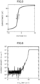
- FIG. 5 shows a graph of results, the horizontal axis indicating a voltage and the vertical axis indicating a capacitance. As shown in FIG. 5 , even after a high electric field (3.3 MV/cm) had been applied to the SiO 2 film, no C-V shift was observed at all. This result indicates that traps in the SiO 2 film are extremely small in amount.
- the MOS capacitor was prepared using the SiO 2 film 3 formed by the method shown in FIGS. 1(A) to 1(D) , and insulating properties of the SiO 2 film 3 were evaluated. Specifically, a positive voltage was applied to the MOS capacitor, and I-V characteristics were measured.
- FIG. 6 shows a graph of results, the horizontal axis indicating an electric field (V/t ox ; t ox is the thickness of the SiO 2 film 3) and the vertical axis indicating a current density.
- breakdown of the SiO 2 film 3 occurred at an electric field of 10 MVcm -1 , and favorable insulating properties were exhibited.
- a Fowler-Nordheim tunnel current was observed within a range of 6 to 9 MVcm -1 . This indicates that defects in the SiO 2 film is small in amount.
- FIG. 7 shows a graph of results, the horizontal axis indicating a position in a film thickness direction, zero indicating the interface between the SiO 2 film 3 and the SiC substrate 1, a positive side indicating a position in the SiC substrate, and a negative side indicating a position in the SiO 2 film. Moreover, the vertical axis indicates a nitrogen atom density.
- nitrogen atoms were present at a density of about 2 ⁇ 10 21 cm -3 at the interface between the SiO 2 film 3 and the SiC substrate 1. Further, nitrogen atoms were also distributed at a density of about 1 ⁇ 10 21 cm -3 in the SiO 2 film.
- the surface of the SiC substrate 1 from which the oxide film has been removed after sacrificial oxidation of the surface is etched with high-temperature H 2 gas, so that the defects remaining in the vicinity of the surface of the SiC substrate 1 can be significantly reduced.
- the SiC substrate 1 is thermally treated in N 2 gas atmosphere after the SiO 2 film 3 has been formed on the surface of the SiC substrate 1 under the conditions where the SiC substrate 1 is not oxidized, so that oxidation of the surface of the SiC substrate 1 can be prevented. Accordingly, the defect density at the interface between the SiO 2 film and the SiC substrate can be significantly reduced, and the SiO 2 film can be obtained with a high quality and stable properties.
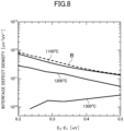
- FIG. 8 shows graphs of results of measurement of the interface defect density in a case where a temperature in etching of the surface of the SiC substrate 1 with high-temperature H 2 gas is 1100°C, 1200°C, and 1300°C. Note that measurement was performed by the above-described high-low CV method. Moreover, a dashed graph indicated by B in the figure indicates a case where no etching with high-temperature H 2 gas was performed.
- FIG. 8 shows that the interface defect density is significantly reduced at a temperature of 1200°C or more.
- almost no effect of the etching with H 2 gas was observed at a temperature of 1100°C. This may be because the SiC substrate was etched little at a temperature of 1100°C.
- a temperature of 1400°C or more is a temperature exceeding the melting point of Si, and for this reason, it is difficult to maintain the chemical composition of the SiC substrate surface at a normal value.
- the etching with H 2 gas is preferably performed within a temperature range of 1200°C to 1300°C.
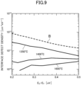
- FIG. 9 shows graphs of results of measurement of the interface defect density in a case where a temperature in the thermal treatment (the interface nitridation treatment) of the SiC substrate 1 in N 2 gas atmosphere after formation of the SiO 2 film 3 on the surface of the SiC substrate 1 is 1350°C, 1400°C, and 1600°C. Note that measurement was performed by the above-described high-low CV method. Moreover, a dashed graph indicated by B in the figure indicates a case where no etching with high-temperature H 2 gas was performed (the interface nitridation treatment was performed with NO gas).
- FIG. 9 shows that the interface defect density is significantly reduced at a temperature of 1350°C or more.
- the thermal treatment (the interface nitridation treatment) in N 2 gas atmosphere is preferably performed within a temperature range of 1350°C to 1600°C.
- FIG. 10 shows graphs of results of measurement of the nitrogen atom density at the SiO 2 /SiC interface in a case where a temperature in the thermal treatment (the interface nitridation treatment) in N 2 gas atmosphere is 1350°C and 1600°C. Note that measurement was performed by the above-described secondary ion mass spectrometry (SIMS).
- SIMS secondary ion mass spectrometry
- the nitrogen atoms are present at a density of 2 ⁇ 10 19 cm -3 or more at the interface between the SiC substrate and the SiO 2 film and in the SiO 2 film.
- the method for manufacturing the SiC semiconductor device in the present embodiment includes a step of etching the surface of the SiC substrate 1 with H 2 gas at a temperature of 1200°C or more, a step of depositing the Si thin film 2 on the SiC substrate 1 by the CVD method, a step of thermally oxidizing the Si thin film 2 at the temperature at which the SiC substrate 1 is not oxidized to form the SiO 2 film 3, and a step of thermally treating the SiC substrate 1 formed with the SiO 2 film 3 in N 2 gas atmosphere at a temperature of 1350°C or more.
- the defect density at the interface between the SiO 2 film 3 and the SiC substrate 1 can be significantly reduced, and the SiO 2 film 3 can be obtained with a high quality and stable properties.
- the SiO 2 film 3 is formed in such a manner that the Si thin film 2 is thermally oxidized at the temperature at which the SiC substrate 1 is not oxidized after the Si thin film 2 has been deposited on the SiC substrate 1.
- the surface of the SiC substrate 1 is not oxidized.
- the thermal treatment in high-temperature N 2 gas atmosphere is, after formation of the SiO 2 film 3, performed as the interface nitridation treatment so that the state in which the surface of the SiC substrate 1 is not oxidized can be maintained.
- the defect density at the interface between the SiO 2 film 3 and the SiC substrate 1 can be significantly reduced in such a manner that the SiC substrate 1 formed with the SiO 2 film 3 is subsequently thermally treated in high-temperature N 2 gas atmosphere.
- FIGS. 11(A) to 11(C) are views showing another method for forming the SiO 2 film on the SiC substrate under the conditions where the SiC substrate is not oxidized.
- the surface of the SiC substrate 1 is, as the pretreatment step, etched with high-temperature H 2 gas.
- the etching with H 2 gas may be performed under conditions of a H 2 flow rate: 1000 sccm, a temperature: 1300°C, a pressure: 0.1 MPa, and a time: 3 minutes, for example.
- one formed with the SiC epitaxial layer (not shown) on the SiC substrate 1 may be used as the SiC substrate 1.
- the oxide film is preferably removed after sacrificial oxidation of the surface of the SiC epitaxial layer.
- the etching with H 2 gas is preferably performed under Si excess atmosphere.
- SiH 4 gas may be, at a flow rate of about 0.01 to 0.1 sccm, added to H 2 gas.
- a SiO 2 film 4 is deposited on the SiC substrate 1 by a plasma CVD method.
- the SiO 2 film 4 may be deposited under the conditions where the SiC substrate 1 is not oxidized, such as a tetraethoxysilane (TEOS) flow rate: 0.3 sccm, an O 2 flow rate: 450 sccm, a temperature: 400°C, a pressure: 43 Pa, a high-frequency power: 100 W, and a time: 30 minutes.
- TEOS tetraethoxysilane
- the SiO 2 film 4 may be performed by a thermal CVD method.
- the SiO 2 film 4 may be performed under the conditions where the SiC substrate 1 is not oxidized, such as a SiH 4 flow rate: 5 sccm, a N 2 O flow rate: 300 sccm, a N 2 flow rate: 3000 sccm, a temperature: 720°C, a pressure: 15 kPa, and a time: 4 minutes.
- the surface of the SiC substrate 1 is slightly oxidized at an initial stage of deposition in some cases.
- an extremely-thin Si layer about one- to three-monolayer-thick Si film, is formed on the surface of the SiC substrate 1 in such a manner that the etching with H 2 gas as shown in FIG. 11(A) is performed in Si excess atmosphere, and therefore, only these extremely-thin Si layers are oxidized, and the surface of the SiC substrate 1 is not oxidized.
- the SiC substrate 1 formed with the SiO 2 film 4 is thermally treated in N 2 gas atmosphere, as shown in FIG. 11(C) .
- the thermal treatment may be performed under conditions such as a N 2 flow rate: 500 sccm, a temperature: 1600°C, a pressure: 1 atmospheric pressure, and a time: 1 minute.
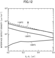
- FIG. 12 shows graphs of dependency of the H 2 gas etching temperature on the interface defect density at an interface between the SiO 2 film 4 and the SiC substrate 1 when the SiO 2 film 4 is formed by the method shown in FIGS. 11(A) to 11(C) . Note that measurement was performed by the above-described high-low CV method. Moreover, a dashed graph indicated by B in the figure indicates a case where no etching with high-temperature H 2 gas was performed (the interface nitridation treatment was performed with NO gas).
- FIG. 12 shows that the interface defect density is significantly reduced at a temperature of 1200°C or more.
- almost no effect of the etching with H 2 gas was observed at a temperature of 1100°C. This may be because the SiC substrate was etched little at a temperature of 1100°C.
- a temperature of 1400°C or more is a temperature exceeding the melting point of Si, and for this reason, it is difficult to maintain the chemical composition of the SiC substrate surface at a normal value.
- the etching with H 2 gas is preferably performed within a temperature range of 1200°C to 1300°C.
- FIG. 13 shows graphs of results of measurement of the interface defect density in a case where a temperature in the thermal treatment (the interface nitridation treatment) of the SiC substrate 1 in N 2 gas atmosphere after formation of the SiO 2 film 4 on the surface of the SiC substrate 1 is 1300°C, 1400°C, 1450°C, and 1600°C. Note that measurement was performed by the above-described high-low CV method. Moreover, a dashed graph indicated by B in the figure indicates a case where no etching with high-temperature H 2 gas was performed (the interface nitridation treatment was performed with NO gas).
- FIG. 13 shows that the interface defect density is significantly reduced at a temperature of 1400°C or more.
- the thermal treatment (the interface nitridation treatment) in N 2 gas atmosphere is preferably performed within a temperature range of 1350°C to 1600°C.
- FIG. 14 shows graphs of results of measurement of the nitrogen atom density at the interface between the SiO 2 film 4 and the SiC substrate 1. Measurement was performed by the above-described secondary ion mass spectrometry (SIMS).
- SIMS secondary ion mass spectrometry
- the horizontal axis indicates a position in a film thickness direction, zero indicates the interface between the SiO 2 film 4 and the SiC substrate 1, a positive side indicates a position in the SiC substrate, and a negative side indicates a position in the SiO 2 film.
- the vertical axis indicates a nitrogen atom density.
- the graph indicated by G in the figure shows a case where the H 2 gas etching was performed as the pretreatment at 1300°C and the thermal treatment with N 2 gas was performed as the interface nitridation treatment at 1600°C.
- the graph indicated by H shows a case where the H 2 gas etching was not performed as the pretreatment and the thermal treatment with NO gas was performed as the interface nitridation treatment.
- nitrogen atoms are present at a density of about 2 ⁇ 10 21 cm -3 at the interface between the SiO 2 film 4 and the SiC substrate 1. Further, nitrogen atoms were also distributed at a density of about 1 ⁇ 10 20 cm -3 or more in the SiO 2 film. Note that although not shown in FIG. 14 , distribution of nitrogen atoms at a density of about 2 ⁇ 10 19 cm -3 or more in the SiO 2 film was confirmed even in a case where the thermal treatment with N 2 gas was performed at 1350°C as in that shown in FIG. 10 .
- nitrogen atoms are present at a density of about 2 ⁇ 10 21 cm -3 at the interface between the SiO 2 film 4 and the SiC substrate 1, but almost no nitrogen atoms are distributed in the SiO 2 film.
- FIG. 15 shows graphs of results of measurement of a difference in the defect density at the interface between the SiO 2 film 4 and the SiC substrate 1 between the case of performing the etching with high-temperature H 2 gas in Si excess atmosphere and the case of not performing the etching in Si excess atmosphere.
- the graph indicated by J shows the case of performing the etching in Si excess atmosphere
- the graph indicated by K shows the case of not performing the etching in Si excess atmosphere.
- the etching with high-temperature H 2 gas was performed under conditions of a H 2 flow rate: 1000 sccm, a temperature: 1300°C, a pressure: 0.1 MPa, and a time: 3 minutes.
- SiH 4 gas was added at a flow rate: 0.05 sccm.
- the thermal treatment in N 2 gas atmosphere was performed under conditions of a N 2 flow rate: 500 sccm, a temperature: 1450°C, a pressure: 1 atmospheric pressure, and a time: 1 minute.
- the interface defect density was significantly reduced to 3 ⁇ 10 10 cm -2 eV -1 or less.
- the interface defect density was not sufficiently reduced even by SiO 2 film deposition and the high-temperature N 2 treatment subsequently performed under optimal conditions, and a high-quality interface was not obtained. This may be because the extremely-thin Si films are not formed on the SiC substrate surface and the surface of the SiC substrate is oxidized at an initial stage of depositing the SiO 2 film.
- the method for manufacturing the SiC semiconductor device in the present embodiment includes a step of etching the surface of the SiC substrate 1 with H 2 gas at a temperature of 1200°C or more in Si excess atmosphere, a step of forming the SiO 2 film 4 on the SiC substrate 1 by the CVD method, and a step of thermally treating the SiC substrate 1 formed with the SiO 2 film 4 in N 2 gas atmosphere at a temperature of 1350°C or more.
- the SiC semiconductor device (the SiC MOSFET) can be formed using, as a gate insulating film, the SiO 2 film formed by the manufacturing method of the present embodiment.
- the nitrogen atoms are present at a density of 2 ⁇ 10 19 cm -3 or more at the interface between the SiC substrate and the SiO 2 film and in the SiO 2 film.
- the interface defect density at the interface between the SiC substrate and the SiO 2 film in the vicinity of the energy lower than the conduction band edge by 0.3 eV is 3 ⁇ 10 10 cm -2 eV -1 or less.
- the density at the energy lower than the conduction band edge by 1.0 eV and the density at the energy higher than the valance band end by 0.7 eV are 5 ⁇ 10 11 cm -3 or less.
- the SiC epitaxial layer is formed on the surface of the SiC substrate, and the SiO 2 film is formed on the SiC epitaxial layer.
- the SiO 2 film may be directly formed on the SiC substrate.
- the manufacturing method of the present invention is also applicable to a SiC substrate for which sacrificial oxidation is not performed.
Landscapes
- Formation Of Insulating Films (AREA)
- Insulated Gate Type Field-Effect Transistor (AREA)
Abstract
Description
- The present invention relates to a silicon carbide (SiC) semiconductor device manufacturing method and a SiC semiconductor device.
- In a case where a SiO2 film (a gate oxide film) is formed on a surface of a SiC substrate by thermal oxidation in a MOS transistor (SiC MOSFET) using the SiC substrate, there is a problem that a defect density at an interface between the SiO2 film and the SiC substrate is extremely high. With a high interface defect density, the characteristics of the SiC MOSFET, such as channel mobility, cannot be sufficiently obtained.
- As a method for reducing the interface defect density,
Patent Document 1 discloses a method in which instead of directly forming a SiO2 film on a surface of a SiC substrate by thermal oxidation, a Si thin film is deposited on the surface of the SiC substrate and the SiO2 film is subsequently formed by oxidation of the Si thin film. - As another method for reducing the interface defect density, Non-Patent
Document 1 discloses a method (interface nitridation) in which thermal treatment is performed in nitric oxide (NO) gas atmosphere after a SiO2 film has been formed on a surface of a SiC substrate by thermal oxidation to nitride an interface between the SiO2 film and the SiC substrate. - PATENT DOCUMENT 1:
Japanese Unexamined Patent Publication No. 11-067757 -
- NON-PATENT DOCUMENT 1: G.Y. Chung et al., IEEE Electron Device Lett., vol. 22, 176 (2001)
- NON-PATENT DOCUMENT 2: K. Kawahara et al., Appl. Phys. Express, vol. 6, 051301 (2013)
- NON-PATENT DOCUMENT 3: F. Devynck et al., Phys. Rev. B, vol. 84, 235320 (2011)
- NON-PATENT DOCUMENT 4: K. Kawahara et al., J. Appl. Phys. vol. 113, 033705 (2013)
- The defect density at the interface between the SiO2 film and the SiC substrate can be significantly reduced by the methods disclosed in the above-described documents, but the interface defect density is still high and greatly limits the characteristics of the SiC MOSFET. The method in which the interface between the SiO2 film and the SiC substrate is nitrided by the NO thermal treatment progresses not only interface nitridation but also oxidation, and for this reason, is a competing process of "nitridation" and "oxidation" and is difficult to be optimized. In addition, NO gas is highly poisonous, and for this reason, is unsuitable for use in mass production.
- The present invention has been made in view of the above-described points, and a main object thereof is to provide a SiC semiconductor device manufacturing method capable of significantly reducing a defect density at an interface between a SiO2 film and a SiC substrate.
- The SiC semiconductor device manufacturing method according to the present invention includes a step of etching a surface of a SiC substrate with H2 gas at a temperature of 1200°C or more, a step of forming a SiO2 film on the SiC substrate under conditions where the SiC substrate is not oxidized, and a step of thermally treating the SiC substrate formed with the SiO2 film in N2 gas atmosphere at a temperature of 1350°C or more.
- According to the present invention, the SiC semiconductor device manufacturing method capable of significantly reducing the defect density at the interface between the SiO2 film and the SiC substrate can be provided.
-
- [
FIG. 1] FIGS. 1(A) to 1(D) show views of a SiC semiconductor device manufacturing method in one embodiment of the present invention. - [
FIG. 2] FIG. 2 shows graphs of a defect density at an interface between a SiO2 film and a SiC substrate. - [
FIG. 3] FIG. 3 shows graphs of the types of defects on a SiC substrate side. - [
FIG. 4] FIG. 4 shows graphs of the types of defects on the SiC substrate side. - [
FIG. 5] FIG. 5 shows a graph of C-V characteristics of the SiO2 film/the SiC substrate. - [
FIG. 6] FIG. 6 shows a graph of I-V characteristics of the SiO2 film. - [
FIG. 7] FIG. 7 shows a graph of a nitrogen atom density in the vicinity of the interface between the SiO2 film and the SiC substrate. - [
FIG. 8] FIG. 8 shows graphs of dependency of a H2 gas etching temperature on an interface defect density. - [
FIG. 9] FIG. 9 shows graphs of dependency of a N2 gas thermal treatment temperature on the interface defect density. - [
FIG. 10] FIG. 10 shows graphs of the nitrogen atom density in the vicinity of the SiO2/SiC interface. - [
FIG. 11] FIGS. 11(A) to 11(C) show views of a SiC semiconductor device manufacturing method in another embodiment of the present invention. - [
FIG. 12] FIG. 12 shows graphs of dependency of a H2 gas etching temperature on an interface defect density. - [
FIG. 13] FIG. 13 shows graphs of dependency of a N2 gas thermal treatment temperature on the interface defect density. - [
FIG. 14] FIG. 14 shows graphs of a nitrogen atom density in the vicinity of the SiO2/SiC interface. - [
FIG. 15] FIG. 15 shows graphs of an effect of high-temperature H2 etching in Si excess atmosphere. - Before description of embodiments of the present invention, a situation that led up to the present invention will be described.
- Upon manufacturing of a semiconductor device by use of a SiC substrate, a step of removing, with a chemical solution of, e.g., hydrofluoric acid, an oxide film formed on a surface of the SiC substrate after sacrificial oxidation of the surface of the SiC substrate is normally performed before the start of a semiconductor device manufacturing step or in the middle of the manufacturing step. In this manner, an impurity having unintentionally adhered to the surface and damage (e.g., chemical composition deviation) of a SiC crystal in the vicinity of an outermost surface can be removed, leading to stability in the characteristics of the semiconductor device and improvement in a yield.
- Certainly, removal of the oxide film after sacrificial oxidation is effective to remove, e.g., the impurity having adhered to the surface of the SiC substrate and damage of the SiC crystal in the vicinity of the outermost surface, but there is a probability of many defects remaining in the surface of the SiC substrate. Actually, it has been known that due to oxidation of the SiC crystal, point defects are densely generated in the vicinity of the SiC surface (Non-Patent Document 2). Moreover, there has also been a theoretical calculation report that due to oxidation of the SiC crystal, interface defects are caused by excessive C atoms at an interface between the oxide film and SiC (Non-Patent Document 3). As described above, it is assumed that if the SiC crystal is oxidized only a little, a large amount of interface defects and SiC-side point defects cannot be avoided.
- For verification, the inventor(s) of the present application et al. have conducted study on pretreatment before formation of a SiO2 film on the surface of the SiC substrate, which is etching of the surface of the SiC substrate, from which the oxide film has been removed after sacrificial oxidation, with high-temperature H2 gas. In addition, the inventor(s) of the present application et al. have also conducted study on N2 thermal treatment as interface nitridation treatment for preventing an oxide film at an interface between the SiO2 film and the SiC substrate in interface nitridation treatment by NO thermal treatment.
- For verifying an effect of the high-temperature H2 gas etching as the pretreatment and an effect of the N2 thermal treatment as the interface nitridation treatment, a sample formed with a SiO2 film on a surface of a SiC substrate was prepared by a method shown in
FIGS. 1(A) to 1(D) . - As shown in
FIG. 1(A) , a surface of aSiC substrate 1 was, as a pretreatment step, etched with high-temperature H2 gas. The etching with H2 gas was performed under conditions of a H2 flow rate: 1000 sccm, a temperature: 1300°C, a pressure: 0.1 MPa, and a time: 3 minutes. - Note that one formed with a SiC epitaxial layer (not shown) on the
SiC substrate 1 was used as theSiC substrate 1. An n-type 4H-SiC(0001) substrate was used as theSiC substrate 1, and the donor concentration of a SiC epitaxial growth layer was 5 × 1015 cm-3. Before the pretreatment step, an oxide film was removed after sacrificial oxidation of a surface of the SiC epitaxial layer. - Next, a Si
thin film 2 was deposited on theSiC substrate 1 by a CVD method, as shown inFIG. 1(B) . The Sithin film 2 was deposited under conditions of a SiH4 flow rate: 50 sccm, a H2 flow rate: 50 sccm, a temperature: 630°C, a pressure: 173 Pa, and a time: 90 seconds. In this manner, the Sithin film 2 with a thickness of about 18 nm was formed on theSiC substrate 1. - Next, the Si
thin film 2 was thermally oxidized, and a SiO2 film 3 was formed accordingly, as shown inFIG. 1(C) . The Sithin film 2 was thermally oxidized under conditions of an O2 flow rate: 2000 sccm, a temperature: 750°C, and a time: 24 hours. Note that these conditions are preferably within a temperature range of 750 to 850°C under conditions where theSiC substrate 1 is not oxidized. If the temperature exceeds 850°C, it is not preferred because of a probability of theSiC substrate 1 being oxidized. - Next, the
SiC substrate 1 formed with the SiO2 film 3 was thermally annealed in N2 gas atmosphere, as shown inFIG. 1(D) . Conditions for the thermal treatment were an N2 flow rate: 500 sccm, a temperature: 1600°C, a pressure: 1 atmospheric pressure, and a time: 1 minute. - Note that for comparison, a sample was prepared in such a manner that a SiO2 film is formed on a SiC substrate by NO gas thermal treatment as the interface nitridation treatment shown in
FIG. 1(D) without the pretreatment by etching with high-temperature H2 gas as shown inFIG. 1(A) . - A MOS capacitor was prepared using the SiO2 film 3 formed by the method shown in
FIGS. 1(A) to 1(D) , and a defect density at an interface between the SiO2 film 3 and theSiC substrate 1 was obtained by a high-low CV method. -
FIG. 2 shows graphs of results, the horizontal axis indicating an energy (ET) from a conduction band edge (EC) and the vertical axis indicating the interface defect density. The graph indicated by A shows a case where the etching with high-temperature H2 gas was performed as the pretreatment and the thermal treatment with N2 gas was performed at the interface nitridation treatment, and the graph indicated by B shows a case where the etching with high-temperature H2 gas was not performed as the pretreatment and the thermal treatment with NO gas was performed as the interface nitridation treatment. - As shown in
FIG. 2 , the sample (the graph A) subjected to the H2 gas etching as the pretreatment shows that an interface defect level density (hereinafter merely referred to as an "interface defect density") was 3 × 1010 cm-2eV-1 or less across a wide energy range and was significantly reduced as compared to the sample (the graph B) not subjected to the H2 gas etching as the pretreatment. - Particularly, in the vicinity of an energy lower than the conduction band edge (EC) by 0.3 eV, the interface defect density was 3 × 1010 cm-2eV-1 or less. This energy range is close to a Fermi level upon ON (current flow) of an n-channel MOSFET, and therefore, a low defect density in this energy range means that a channel resistance in a SiC MOSFET can be significantly reduced.
- Such analysis results show that many defects remain in the surface of the
SiC substrate 1 from which the oxide film was removed after sacrificial oxidation of the surface and it is effective to etch the surface of theSiC substrate 1 with high-temperature H2 gas in order to efficiently remove these defects. - The MOS capacitor was prepared using the SiO2 film 3 formed by the method shown in
FIGS. 1(A) to 1(D) , and defects on a SiC substrate side were analyzed. Specifically, the types of defects on the SiC substrate side were analyzed by a deep level transient spectroscopy (DLTS) method. -
FIG. 3 shows graphs of results, the horizontal axis indicating a temperature and the vertical axis indicating a DLTS signal. The graph indicated by C shows a case where the etching with high-temperature H2 gas was performed as the pretreatment and the thermal treatment with N2 gas was performed as the interface nitridation treatment. Moreover, the graph indicated by D shows a case where the etching with high-temperature H2 gas was not performed as the pretreatment and the thermal treatment with NO gas was performed as the interface nitridation treatment. - As shown in
FIG. 3 , in the sample (the graph C) subjected to the thermal treatment with N2 gas, only a peak indicated by an arrow Z was observed. On the other hand, in the sample (the graph D) subjected to the thermal treatment with NO gas, three peaks indicated by arrows N1, N2, N3 were observed in addition to a peak indicated by an arrow Z. It has been known that the peak indicated by the arrow Z is due to a crystal fault (a carbon vacancy) created in theSiC substrate 1 upon SiC crystal growth. On the other hand, the peaks indicated by the arrows N1, N2, N3 correspond to defects generated in the vicinity of the SiC surface due to thermal oxidation of the SiC substrate 1 (Non-Patent Document 2). - These results show that in a case where the thermal treatment with NO gas is performed as the interface nitridation treatment, the surface of the
SiC substrate 1 is slightly oxidized during the interface nitridation treatment. On the other hand, the results show that in a case where the thermal treatment with N2 gas is performed as the interface nitridation treatment, the surface of theSiC substrate 1 is not oxidized. - Moreover, these results indicate that even when the SiC surface is cleaned and the quality thereof is enhanced by the high-temperature H2 gas etching, if SiC is oxidized even a little in a step thereafter, a sufficiently-low interface defect density cannot be obtained.
- For example, the sample subjected to the interface nitridation treatment with NO gas has been described above, but similar DLTS peaks N1, N2, N3 were also observed in a sample for which a Si
thin film 2 was deposited after the etching with high-temperature H2 gas and the nitridation treatment with N2 gas was performed at a high temperature (1600°C) after formation of a SiO2 film 3 by high-temperature (950°C) oxidation. This means that a surface of theSiC substrate 1 is oxidized upon the oxidation treatment at 950°C. - That is, even if defects in the vicinity of the SiC substrate surface are removed by the high-temperature H2 gas etching, if oxidation is performed at a high temperature (950°C) upon formation of the SiO2 film 3 by oxidation of the Si
thin film 2, the surface of theSiC substrate 1 is slightly oxidized. For this reason, even if the nitridation treatment with N2 gas is performed thereafter at a high temperature (1600°C), a sufficiently-low interface defect density cannot be obtained. - Note that the sample used for verification was prepared using the n-type SiC substrate, but the types of defects on the SiC substrate side were also analyzed by the DLTS method for a sample prepared using a p-type SiC substrate by the same method as that shown in
FIGS. 1(A) to 1(D) . -
FIG. 4 shows graphs of results, and the graph indicated by C shows a case where the H2 gas etching was performed as the pretreatment and the thermal treatment with N2 gas was performed as the interface nitridation treatment. Moreover, the graph indicated by D shows a case where the H2 gas etching was not performed as the pretreatment and the thermal treatment with NO gas was performed as the interface nitridation treatment. - As shown in
FIG. 4 , in the sample (the graph C) subjected to the thermal treatment with N2 gas, no peak due to a point defect in a SiC crystal was observed. However, in the sample (the graph D) subjected to the thermal treatment with NO gas, a peak indicated by an arrow P1 was observed. It has been known that the peak indicated by P1 is due to a defect generated in the vicinity of the SiC surface due to thermal oxidation of the SiC substrate 1 (Non-Patent Document 4). - These results show that even in the case of using the p-type SiC substrate, the surface of the
SiC substrate 1 was oxidized in the case of performing the thermal treatment with the NO gas as the interface nitridation treatment, but was not oxidized in the case of performing the thermal treatment with N2 gas. - Table 1 shows energy positions and defect densities for the types OX-N1, OX-N2, OX-N3, OX-P1 of defects indicated by the arrows N1 to N3, P1. Here, Ec is an energy level at the conduction band edge, and Ev is an energy level at a valance band edge. Note that the energy position was obtained by analysis of dependency, which is obtained by DLTS measurement, of a temperature on the time constant of carrier emission. Moreover, the defect density was obtained from a peak intensity obtained in DLTS measurement.
[Table 1] Type of Defect Energy Position Defect Density OX-N1 Ec - 0.8 eV up to 1 × 1013 cm-3 OX-N2 Ec - 1.0 eV up to 5 × 1012 cm-3 OX-N3 Ec - 1.6 eV up to 2 × 1013 cm-3 OX-P1 Ev + 0.7 eV up to 1 × 1013 cm-3 - From Table 1, in a case where the H2 thermal treatment is performed as the pretreatment and the thermal treatment with N2 gas is performed as the interface nitridation treatment, point defects on the SiC substrate side are estimated, for the following reason, such that a point defect density at an energy lower than the conduction band edge by 1.0 eV is 5 × 1011 cm-3 or less. Moreover, it is estimated that a point defect density at an energy higher than the valance band edge by 0.7 eV is 5 × 1011 cm-3 or less.
- That is, no DLTS peaks corresponding to these point defects are observed in the sample subjected to the H2 thermal treatment as the pretreatment and the thermal treatment with N2 gas as the interface nitridation treatment, as shown in
FIGS. 3 and 4 . As a result of simulation of DLTS peaks by numerical calculation by use of the properties of defects observed in other samples, it has been found that if the point defect density is at least 5 × 1011 cm-3 or more, significant DLTS peaks are observed under these measurement conditions. Thus, it is estimated that a point defect density on the SiC substrate side in an unoxidized sample is 5 × 1011 cm-3 or less. - For the SiO2 film 3 formed by the method shown in
FIGS. 1(A) to 1(D) , e.g., the properties of the SiO2 film were evaluated by the following method in order to check the effect of the etching with high-temperature H2 gas and the effect of the N2 thermal treatment as the interface nitridation treatment. - The MOS capacitor was prepared using the SiO2 film 3 formed by the method shown in
FIGS. 1(A) to 1(D) , and a property shift by voltage stress was evaluated. Specifically, a voltage of 10 V was applied to the MOS capacitor for 300 seconds, and thereafter, a bias was swept from a positive voltage to a negative voltage. Then, a voltage of -10 V was applied for 300 seconds, and thereafter, the bias was swept from the negative voltage to the positive voltage. Then, a C-V property shift was measured. -
FIG. 5 shows a graph of results, the horizontal axis indicating a voltage and the vertical axis indicating a capacitance. As shown inFIG. 5 , even after a high electric field (3.3 MV/cm) had been applied to the SiO2 film, no C-V shift was observed at all. This result indicates that traps in the SiO2 film are extremely small in amount. - The MOS capacitor was prepared using the SiO2 film 3 formed by the method shown in
FIGS. 1(A) to 1(D) , and insulating properties of the SiO2 film 3 were evaluated. Specifically, a positive voltage was applied to the MOS capacitor, and I-V characteristics were measured. -
FIG. 6 shows a graph of results, the horizontal axis indicating an electric field (V/tox; tox is the thickness of the SiO2 film 3) and the vertical axis indicating a current density. As shown inFIG. 6 , breakdown of the SiO2 film 3 occurred at an electric field of 10 MVcm-1, and favorable insulating properties were exhibited. Moreover, a Fowler-Nordheim tunnel current was observed within a range of 6 to 9 MVcm-1. This indicates that defects in the SiO2 film is small in amount. - In order to verify the effect of the interface nitridation treatment with N2 gas, a nitrogen atom density at the interface between the SiO2 film 3 and the
SiC substrate 1 was measured by secondary ion mass spectrometry (SIMS). -
FIG. 7 shows a graph of results, the horizontal axis indicating a position in a film thickness direction, zero indicating the interface between the SiO2 film 3 and theSiC substrate 1, a positive side indicating a position in the SiC substrate, and a negative side indicating a position in the SiO2 film. Moreover, the vertical axis indicates a nitrogen atom density. - As shown in
FIG. 7 , nitrogen atoms were present at a density of about 2 × 1021 cm-3 at the interface between the SiO2 film 3 and theSiC substrate 1. Further, nitrogen atoms were also distributed at a density of about 1 × 1021 cm-3 in the SiO2 film. - These results show that the nitrogen atoms are, at a sufficient density, introduced into the interface between the SiO2 film and the SiC substrate and into the SiO2 film by the thermal treatment with N2 gas. Accordingly, it is assumed that the defect density at the interface between the SiO2 film and the SiC substrate is sufficiently reduced.
- According to the above-described results, the surface of the
SiC substrate 1 from which the oxide film has been removed after sacrificial oxidation of the surface is etched with high-temperature H2 gas, so that the defects remaining in the vicinity of the surface of theSiC substrate 1 can be significantly reduced. Moreover, theSiC substrate 1 is thermally treated in N2 gas atmosphere after the SiO2 film 3 has been formed on the surface of theSiC substrate 1 under the conditions where theSiC substrate 1 is not oxidized, so that oxidation of the surface of theSiC substrate 1 can be prevented. Accordingly, the defect density at the interface between the SiO2 film and the SiC substrate can be significantly reduced, and the SiO2 film can be obtained with a high quality and stable properties. -
FIG. 8 shows graphs of results of measurement of the interface defect density in a case where a temperature in etching of the surface of theSiC substrate 1 with high-temperature H2 gas is 1100°C, 1200°C, and 1300°C. Note that measurement was performed by the above-described high-low CV method. Moreover, a dashed graph indicated by B in the figure indicates a case where no etching with high-temperature H2 gas was performed. -
FIG. 8 shows that the interface defect density is significantly reduced at a temperature of 1200°C or more. On the other hand, almost no effect of the etching with H2 gas was observed at a temperature of 1100°C. This may be because the SiC substrate was etched little at a temperature of 1100°C. Note that a temperature of 1400°C or more is a temperature exceeding the melting point of Si, and for this reason, it is difficult to maintain the chemical composition of the SiC substrate surface at a normal value. Thus, in order to obtain an effect of reducing the interface defect density, the etching with H2 gas is preferably performed within a temperature range of 1200°C to 1300°C. -
FIG. 9 shows graphs of results of measurement of the interface defect density in a case where a temperature in the thermal treatment (the interface nitridation treatment) of theSiC substrate 1 in N2 gas atmosphere after formation of the SiO2 film 3 on the surface of theSiC substrate 1 is 1350°C, 1400°C, and 1600°C. Note that measurement was performed by the above-described high-low CV method. Moreover, a dashed graph indicated by B in the figure indicates a case where no etching with high-temperature H2 gas was performed (the interface nitridation treatment was performed with NO gas). -
FIG. 9 shows that the interface defect density is significantly reduced at a temperature of 1350°C or more. On the other hand, almost no effect of the N2 gas thermal treatment was observed at a temperature of less than 1350°C. This may be because the nitrogen atoms were not introduced, at a sufficient density, into the interface between the SiO2 film 3 and theSiC substrate 1 at a temperature of less than 1350°C. Note that thermal decomposition of the SiO2 film surface begins at a temperature of 1700°C or more, and for this reason, it is difficult to maintain the quality of the SiO2 film. Thus, in order to obtain an effect of reducing the interface defect density, the thermal treatment (the interface nitridation treatment) in N2 gas atmosphere is preferably performed within a temperature range of 1350°C to 1600°C. -
FIG. 10 shows graphs of results of measurement of the nitrogen atom density at the SiO2/SiC interface in a case where a temperature in the thermal treatment (the interface nitridation treatment) in N2 gas atmosphere is 1350°C and 1600°C. Note that measurement was performed by the above-described secondary ion mass spectrometry (SIMS). - As shown in
FIG. 10 , in a case where the interface nitridation treatment is performed at a temperature of 1350°C or more, the nitrogen atoms are present at a density of 2 × 1019 cm-3 or more at the interface between the SiC substrate and the SiO2 film and in the SiO2 film. - As described above, the method for manufacturing the SiC semiconductor device in the present embodiment includes a step of etching the surface of the
SiC substrate 1 with H2 gas at a temperature of 1200°C or more, a step of depositing the Sithin film 2 on theSiC substrate 1 by the CVD method, a step of thermally oxidizing the Sithin film 2 at the temperature at which theSiC substrate 1 is not oxidized to form the SiO2 film 3, and a step of thermally treating theSiC substrate 1 formed with the SiO2 film 3 in N2 gas atmosphere at a temperature of 1350°C or more. With this configuration, the defect density at the interface between the SiO2 film 3 and theSiC substrate 1 can be significantly reduced, and the SiO2 film 3 can be obtained with a high quality and stable properties. - In the above-described embodiment, the SiO2 film 3 is formed in such a manner that the Si
thin film 2 is thermally oxidized at the temperature at which theSiC substrate 1 is not oxidized after the Sithin film 2 has been deposited on theSiC substrate 1. Thus, the surface of theSiC substrate 1 is not oxidized. Moreover, the thermal treatment in high-temperature N2 gas atmosphere is, after formation of the SiO2 film 3, performed as the interface nitridation treatment so that the state in which the surface of theSiC substrate 1 is not oxidized can be maintained. - That is, as long as the SiO2 film 3 is, under the conditions where the
SiC substrate 1 is not oxidized, formed on theSiC substrate 1 after etching of the surface of theSiC substrate 1 with high-temperature H2 gas, the defect density at the interface between the SiO2 film 3 and theSiC substrate 1 can be significantly reduced in such a manner that theSiC substrate 1 formed with the SiO2 film 3 is subsequently thermally treated in high-temperature N2 gas atmosphere. -
FIGS. 11(A) to 11(C) are views showing another method for forming the SiO2 film on the SiC substrate under the conditions where the SiC substrate is not oxidized. - As shown in
FIG. 11(A) , the surface of theSiC substrate 1 is, as the pretreatment step, etched with high-temperature H2 gas. The etching with H2 gas may be performed under conditions of a H2 flow rate: 1000 sccm, a temperature: 1300°C, a pressure: 0.1 MPa, and a time: 3 minutes, for example. - Note that one formed with the SiC epitaxial layer (not shown) on the
SiC substrate 1 may be used as theSiC substrate 1. Moreover, before the pretreatment step, the oxide film is preferably removed after sacrificial oxidation of the surface of the SiC epitaxial layer. Note that for the following reason, the etching with H2 gas is preferably performed under Si excess atmosphere. For example, SiH4 gas may be, at a flow rate of about 0.01 to 0.1 sccm, added to H2 gas. - Next, as shown in
FIG. 11(B) , a SiO2 film 4 is deposited on theSiC substrate 1 by a plasma CVD method. The SiO2 film 4 may be deposited under the conditions where theSiC substrate 1 is not oxidized, such as a tetraethoxysilane (TEOS) flow rate: 0.3 sccm, an O2 flow rate: 450 sccm, a temperature: 400°C, a pressure: 43 Pa, a high-frequency power: 100 W, and a time: 30 minutes. - Note that the SiO2 film 4 may be performed by a thermal CVD method. In this case, the SiO2 film 4 may be performed under the conditions where the
SiC substrate 1 is not oxidized, such as a SiH4 flow rate: 5 sccm, a N2O flow rate: 300 sccm, a N2 flow rate: 3000 sccm, a temperature: 720°C, a pressure: 15 kPa, and a time: 4 minutes. - Since O2 gas or N2O gas is contained in reactive gas even in a case where the SiO2 film 4 is deposited under these conditions, the surface of the
SiC substrate 1 is slightly oxidized at an initial stage of deposition in some cases. However, even in this case, an extremely-thin Si layer, about one- to three-monolayer-thick Si film, is formed on the surface of theSiC substrate 1 in such a manner that the etching with H2 gas as shown inFIG. 11(A) is performed in Si excess atmosphere, and therefore, only these extremely-thin Si layers are oxidized, and the surface of theSiC substrate 1 is not oxidized. - Next, the
SiC substrate 1 formed with the SiO2 film 4 is thermally treated in N2 gas atmosphere, as shown inFIG. 11(C) . The thermal treatment may be performed under conditions such as a N2 flow rate: 500 sccm, a temperature: 1600°C, a pressure: 1 atmospheric pressure, and a time: 1 minute. -
FIG. 12 shows graphs of dependency of the H2 gas etching temperature on the interface defect density at an interface between the SiO2 film 4 and theSiC substrate 1 when the SiO2 film 4 is formed by the method shown inFIGS. 11(A) to 11(C) . Note that measurement was performed by the above-described high-low CV method. Moreover, a dashed graph indicated by B in the figure indicates a case where no etching with high-temperature H2 gas was performed (the interface nitridation treatment was performed with NO gas). -
FIG. 12 shows that the interface defect density is significantly reduced at a temperature of 1200°C or more. On the other hand, almost no effect of the etching with H2 gas was observed at a temperature of 1100°C. This may be because the SiC substrate was etched little at a temperature of 1100°C. Note that a temperature of 1400°C or more is a temperature exceeding the melting point of Si, and for this reason, it is difficult to maintain the chemical composition of the SiC substrate surface at a normal value. Thus, in order to obtain an effect of reducing the interface defect density, the etching with H2 gas is preferably performed within a temperature range of 1200°C to 1300°C. -
FIG. 13 shows graphs of results of measurement of the interface defect density in a case where a temperature in the thermal treatment (the interface nitridation treatment) of theSiC substrate 1 in N2 gas atmosphere after formation of the SiO2 film 4 on the surface of theSiC substrate 1 is 1300°C, 1400°C, 1450°C, and 1600°C. Note that measurement was performed by the above-described high-low CV method. Moreover, a dashed graph indicated by B in the figure indicates a case where no etching with high-temperature H2 gas was performed (the interface nitridation treatment was performed with NO gas). -
FIG. 13 shows that the interface defect density is significantly reduced at a temperature of 1400°C or more. On the other hand, almost no effect of the N2 gas thermal treatment was observed at a temperature of less than 1300°C. This may be because the nitrogen atoms were not introduced, at a sufficient density, into the interface between the SiO2 film 3 and theSiC substrate 1 at a temperature of 1300°C. Note that thermal decomposition of the SiO2 film surface begins at a temperature of 1700°C or more, and for this reason, it is difficult to maintain the quality of the SiO2 film. Thus, in order to obtain an effect of reducing the interface defect density, the thermal treatment (the interface nitridation treatment) in N2 gas atmosphere is preferably performed within a temperature range of 1350°C to 1600°C. -
FIG. 14 shows graphs of results of measurement of the nitrogen atom density at the interface between the SiO2 film 4 and theSiC substrate 1. Measurement was performed by the above-described secondary ion mass spectrometry (SIMS). The horizontal axis indicates a position in a film thickness direction, zero indicates the interface between the SiO2 film 4 and theSiC substrate 1, a positive side indicates a position in the SiC substrate, and a negative side indicates a position in the SiO2 film. Moreover, the vertical axis indicates a nitrogen atom density. The graph indicated by G in the figure shows a case where the H2 gas etching was performed as the pretreatment at 1300°C and the thermal treatment with N2 gas was performed as the interface nitridation treatment at 1600°C. Moreover, the graph indicated by H shows a case where the H2 gas etching was not performed as the pretreatment and the thermal treatment with NO gas was performed as the interface nitridation treatment. - As shown in
FIG. 14 , in the case of the etching with high-temperature H2 gas, nitrogen atoms are present at a density of about 2 × 1021 cm-3 at the interface between the SiO2 film 4 and theSiC substrate 1. Further, nitrogen atoms were also distributed at a density of about 1 × 1020 cm-3 or more in the SiO2 film. Note that although not shown inFIG. 14 , distribution of nitrogen atoms at a density of about 2 × 1019 cm-3 or more in the SiO2 film was confirmed even in a case where the thermal treatment with N2 gas was performed at 1350°C as in that shown inFIG. 10 . - On the other hand, also in the case of nitridation of the interface with NO gas, nitrogen atoms are present at a density of about 2 × 1021 cm-3 at the interface between the SiO2 film 4 and the
SiC substrate 1, but almost no nitrogen atoms are distributed in the SiO2 film. - As described above, even in a case where the SiO2 film 4 is deposited on the
SiC substrate 1 under the conditions where theSiC substrate 1 is not oxidized, O2 gas or N2O gas is contained in reactive gas. For this reason, the surface of theSiC substrate 1 is slightly oxidized at the initial stage of deposition in some cases. However, even in this case, an extremely-thin Si layer, about one- to three-monolayer-thick Si film, is formed on the surface of theSiC substrate 1 in such a manner that the etching with high-temperature H2 gas as the pretreatment is performed in Si excess atmosphere, and therefore, only these extremely-thin Si layers are oxidized and the surface of theSiC substrate 1 is not oxidized. -
FIG. 15 shows graphs of results of measurement of a difference in the defect density at the interface between the SiO2 film 4 and theSiC substrate 1 between the case of performing the etching with high-temperature H2 gas in Si excess atmosphere and the case of not performing the etching in Si excess atmosphere. The graph indicated by J shows the case of performing the etching in Si excess atmosphere, and the graph indicated by K shows the case of not performing the etching in Si excess atmosphere. - The etching with high-temperature H2 gas was performed under conditions of a H2 flow rate: 1000 sccm, a temperature: 1300°C, a pressure: 0.1 MPa, and a time: 3 minutes. In the case of performing the etching with high-temperature H2 gas in Si excess atmosphere, SiH4 gas was added at a flow rate: 0.05 sccm. The thermal treatment in N2 gas atmosphere was performed under conditions of a N2 flow rate: 500 sccm, a temperature: 1450°C, a pressure: 1 atmospheric pressure, and a time: 1 minute.
- As shown in
FIG. 15 , in a case where the etching with high-temperature H2 gas was performed in Si excess atmosphere (the graph J), the interface defect density was significantly reduced to 3 × 1010 cm-2eV-1 or less. On the other hand, in a case where the etching with high-temperature H2 gas was not performed in Si excess atmosphere, the interface defect density was not sufficiently reduced even by SiO2 film deposition and the high-temperature N2 treatment subsequently performed under optimal conditions, and a high-quality interface was not obtained. This may be because the extremely-thin Si films are not formed on the SiC substrate surface and the surface of the SiC substrate is oxidized at an initial stage of depositing the SiO2 film. - As a result of analysis of the types of defects on the SiC substrate side by the DLTS method for a sample for which the etching with high-temperature H2 gas was performed in Si excess atmosphere, no defects (no defects indicated by the arrows N1 to N3, P1 shown in
FIGS. 3 and 4 ) caused due to oxidation of the SiC crystal were observed. On the other hand, for a sample for which the etching with high-temperature H2 gas was not performed in Si excess atmosphere, the defects caused due to oxidation of the SiC crystal were observed on the SiC substrate side. This means that the surface of theSiC substrate 1 is oxidized even after the SiO2 film 4 has been deposited on theSiC substrate 1 under the conditions where theSiC substrate 1 is assumed not to be oxidized. - As described above, the method for manufacturing the SiC semiconductor device in the present embodiment includes a step of etching the surface of the
SiC substrate 1 with H2 gas at a temperature of 1200°C or more in Si excess atmosphere, a step of forming the SiO2 film 4 on theSiC substrate 1 by the CVD method, and a step of thermally treating theSiC substrate 1 formed with the SiO2 film 4 in N2 gas atmosphere at a temperature of 1350°C or more. With this configuration, the defect density at the interface between the SiO2 film 4 and theSiC substrate 1 can be significantly reduced, and the SiO2 film 3 can be obtained with a high quality and stable properties. - The SiC semiconductor device (the SiC MOSFET) can be formed using, as a gate insulating film, the SiO2 film formed by the manufacturing method of the present embodiment. In such a SiC semiconductor device, the nitrogen atoms are present at a density of 2 × 1019 cm-3 or more at the interface between the SiC substrate and the SiO2 film and in the SiO2 film.
- The interface defect density at the interface between the SiC substrate and the SiO2 film in the vicinity of the energy lower than the conduction band edge by 0.3 eV is 3 × 1010 cm-2eV-1 or less.
- Of the point defects on the SiC substrate side, the density at the energy lower than the conduction band edge by 1.0 eV and the density at the energy higher than the valance band end by 0.7 eV are 5 × 1011 cm-3 or less.
- The present invention has been described above with reference to the preferred embodiments, but such description is not limited and various modifications may be made thereto, needless to say. For example, in the above-described embodiments, the SiC epitaxial layer is formed on the surface of the SiC substrate, and the SiO2 film is formed on the SiC epitaxial layer. However, the SiO2 film may be directly formed on the SiC substrate.
- In the above-described embodiments, the SiC substrate from which the oxide film has been removed after sacrificial oxidation of the surface is used, but the manufacturing method of the present invention is also applicable to a SiC substrate for which sacrificial oxidation is not performed.
-
- 1
- SiC Substrate
- 2
- Si Thin Film
- 3, 4
- SiO2 Film
Claims (13)
- A SiC semiconductor device manufacturing method comprising:a step (A) of etching a surface of a SiC substrate with H2 gas at a temperature of 1200°C or more;a step (B) of forming a SiO2 film on the SiC substrate under a condition where the SiC substrate is not oxidized; anda step (C) of thermally treating the SiC substrate formed with the SiO2 film in N2 gas atmosphere at a temperature of 1350°C or more.
- The SiC semiconductor device manufacturing method of claim 1, wherein
the step (B) includesa step (B 1) of depositing a Si thin film on the SiC substrate by a CVD method, anda step (B2) of thermally oxidizing the Si thin film at a temperature at which the SiC substrate is not oxidized to form the SiO2 film. - The SiC semiconductor device manufacturing method of claim 1, whereinthe step (A) is executed in Si excess atmosphere, andthe step (B) includes a step (B3) of forming the SiO2 film on the SiC substrate by a CVD method.
- The SiC semiconductor device manufacturing method of claim 3, wherein
in the step (A), a one- to three-monolayer-thick Si film is formed on the surface of the SiC substrate. - The SiC semiconductor device manufacturing method of claim 2, wherein
the step (B2) is executed within a temperature range of 750 to 850°C. - The SiC semiconductor device manufacturing method of claim 1, further comprising:
before the step (A), a step of etching away an oxide film on the surface of the SiC substrate after sacrificial oxidation of the SiC substrate. - The SiC semiconductor device manufacturing method of any one of claims 1 to 6, wherein
after the thermal treatment of the step (C), a nitrogen atom is present at a density of 2 × 1019 cm-3 or more at an interface between the SiC substrate and the SiO2 film and in the SiO2 film. - The SiC semiconductor device manufacturing method of any one of claims 1 to 6, wherein
after the thermal treatment of the step (C), an interface defect density at an interface between the SiC substrate and the SiO2 film in a vicinity of an energy lower than a conduction band end by 0.3 eV is 3 × 1010 cm-2eV-1 or less. - The SiC semiconductor device manufacturing method of any one of claims 1 to 6, wherein
of a point defect on a SiC substrate side after the thermal treatment of the step (C), a density at an energy lower than a conduction band edge by 1.0 eV and a density at an energy higher than a valance band edge by 0.7 eV are 5 × 1011 cm-3 or less. - The SiC semiconductor device manufacturing method of claim 1, wherein
the SiC substrate includes a SiC substrate formed with a SiC epitaxial layer on a surface thereof. - A SiC semiconductor device comprising:a gate insulating film formed of a SiO2 film on a SiC substrate,wherein a nitrogen atom is present at a density of 2 × 1019 cm-3 or more at an interface between the SiC substrate and the SiO2 film and in the SiO2 film.
- A SiC semiconductor device comprising:a gate insulating film formed of a SiO2 film on a SiC substrate,wherein an interface defect density at an interface between the SiC substrate and the SiO2 film in a vicinity of an energy lower than a conduction band end by 0.3 eV is 3 × 1010 cm-2eV-1 or less.
- A SiC semiconductor device comprising:a gate insulating film formed of a SiO2 film on a SiC substrate,wherein of a point defect on a SiC substrate side, a density at an energy lower than a conduction band edge by 1.0 eV and a density at an energy higher than a valance band edge by 0.7 eV are 5 × 1011 cm-3 or less.
Applications Claiming Priority (2)
| Application Number | Priority Date | Filing Date | Title |
|---|---|---|---|
| JP2020098244A JP7412765B2 (en) | 2020-06-05 | 2020-06-05 | SiC semiconductor device manufacturing method and SiC semiconductor device |
| PCT/JP2021/020202 WO2021246280A1 (en) | 2020-06-05 | 2021-05-27 | Sic semiconductor element manufacturing method and sic semiconductor element |
Publications (4)
| Publication Number | Publication Date |
|---|---|
| EP4163955A1 true EP4163955A1 (en) | 2023-04-12 |
| EP4163955A4 EP4163955A4 (en) | 2023-11-15 |
| EP4163955B1 EP4163955B1 (en) | 2024-12-04 |
| EP4163955C0 EP4163955C0 (en) | 2024-12-04 |
Family
ID=78831119
Family Applications (1)
| Application Number | Title | Priority Date | Filing Date |
|---|---|---|---|
| EP21817045.4A Active EP4163955B1 (en) | 2020-06-05 | 2021-05-27 | Sic semiconductor element manufacturing method and sic semiconductor element |
Country Status (5)
| Country | Link |
|---|---|
| US (2) | US12396230B2 (en) |
| EP (1) | EP4163955B1 (en) |
| JP (1) | JP7412765B2 (en) |
| CN (1) | CN115668466B (en) |
| WO (1) | WO2021246280A1 (en) |
Families Citing this family (4)
| Publication number | Priority date | Publication date | Assignee | Title |
|---|---|---|---|---|
| JP7412765B2 (en) * | 2020-06-05 | 2024-01-15 | 国立大学法人京都大学 | SiC semiconductor device manufacturing method and SiC semiconductor device |
| CN115513041B (en) * | 2022-09-23 | 2026-07-17 | 上海积塔半导体有限公司 | SiC substrate processing method, structure and wafer processing method |
| KR102758455B1 (en) | 2023-01-19 | 2025-01-22 | (주)이큐테크플러스 | Method for manufacturing thin film for minimizing the increase in defects at the interface during the high-temperature oxidation process |
| CN117672823A (en) * | 2023-12-04 | 2024-03-08 | 厦门紫硅半导体科技有限公司 | A method for preparing high-quality SiC gate oxide layer |
Family Cites Families (16)
| Publication number | Priority date | Publication date | Assignee | Title |
|---|---|---|---|---|
| JP3143670B2 (en) | 1997-08-13 | 2001-03-07 | 工業技術院長 | Oxide thin film forming method |
| JP2006216918A (en) * | 2005-02-07 | 2006-08-17 | Kyoto Univ | Manufacturing method of semiconductor device |
| JP2006351744A (en) * | 2005-06-15 | 2006-12-28 | Fuji Electric Holdings Co Ltd | Method for manufacturing silicon carbide semiconductor device |
| JP2011049368A (en) * | 2009-08-27 | 2011-03-10 | Mitsubishi Electric Corp | Method of manufacturing silicon carbide semiconductor device |
| JP2011091186A (en) * | 2009-10-22 | 2011-05-06 | Mitsubishi Electric Corp | Method for manufacturing silicon carbide semiconductor device |
| US8546815B2 (en) | 2009-12-16 | 2013-10-01 | National University Corporation NARA Institute of Science and Technology | SiC semiconductor element and manufacturing method for same |
| JP2012004275A (en) * | 2010-06-16 | 2012-01-05 | Sumitomo Electric Ind Ltd | Method of manufacturing silicon carbide semiconductor device |
| WO2012067112A1 (en) * | 2010-11-17 | 2012-05-24 | 新日本製鐵株式会社 | Method for producing epitaxial silicon carbide single crystal substrate |
| JP5460768B2 (en) * | 2012-03-21 | 2014-04-02 | 日産自動車株式会社 | Method for manufacturing silicon carbide semiconductor device |
| JP6162388B2 (en) * | 2012-11-14 | 2017-07-12 | 新日本無線株式会社 | Method for manufacturing silicon carbide semiconductor device |
| CN105531802A (en) * | 2013-07-11 | 2016-04-27 | 富士电机株式会社 | Silicon-carbide semiconductor device and method for manufacturing silicon-carbide semiconductor device |
| JP2015142034A (en) * | 2014-01-29 | 2015-08-03 | ルネサスエレクトロニクス株式会社 | Manufacturing method of semiconductor device |
| JP6432232B2 (en) * | 2014-09-11 | 2018-12-05 | 富士電機株式会社 | Silicon carbide semiconductor device and method for manufacturing silicon carbide semiconductor device |
| CN107785270B (en) * | 2016-08-31 | 2021-05-07 | 株洲中车时代半导体有限公司 | A kind of nitriding method of MOSFET device |
| JP7196458B2 (en) * | 2018-08-13 | 2022-12-27 | 富士電機株式会社 | Method for manufacturing insulated gate semiconductor device |
| JP7412765B2 (en) * | 2020-06-05 | 2024-01-15 | 国立大学法人京都大学 | SiC semiconductor device manufacturing method and SiC semiconductor device |
-
2020
- 2020-06-05 JP JP2020098244A patent/JP7412765B2/en active Active
-
2021
- 2021-05-27 WO PCT/JP2021/020202 patent/WO2021246280A1/en not_active Ceased
- 2021-05-27 EP EP21817045.4A patent/EP4163955B1/en active Active
- 2021-05-27 CN CN202180039705.2A patent/CN115668466B/en active Active
- 2021-05-27 US US18/007,985 patent/US12396230B2/en active Active
-
2025
- 2025-07-25 US US19/280,632 patent/US20250351502A1/en active Pending
Also Published As
| Publication number | Publication date |
|---|---|
| JP2021192397A (en) | 2021-12-16 |
| US12396230B2 (en) | 2025-08-19 |
| CN115668466B (en) | 2026-06-16 |
| US20230307503A1 (en) | 2023-09-28 |
| JP7412765B2 (en) | 2024-01-15 |
| CN115668466A (en) | 2023-01-31 |
| EP4163955B1 (en) | 2024-12-04 |
| EP4163955C0 (en) | 2024-12-04 |
| EP4163955A4 (en) | 2023-11-15 |
| US20250351502A1 (en) | 2025-11-13 |
| WO2021246280A1 (en) | 2021-12-09 |
Similar Documents
| Publication | Publication Date | Title |
|---|---|---|
| EP4163955B1 (en) | Sic semiconductor element manufacturing method and sic semiconductor element | |
| US7709403B2 (en) | Silicon carbide-oxide layered structure, production method thereof, and semiconductor device | |
| US8642476B2 (en) | Method for manufacturing silicon carbide semiconductor device | |
| EP4266354B1 (en) | Sic semiconductor element manufacturing method | |
| Niimi et al. | Monolayer-level controlled incorporation of nitrogen at Si–SiO 2 interfaces using remote plasma processing | |
| JP2006210818A (en) | Semiconductor device and manufacturing method thereof | |
| US20230064865A1 (en) | Semiconductor device and method for manufacturing semiconductor device | |
| EP1608007A1 (en) | Method for forming insulating film in semiconductor device | |
| CN103262225A (en) | Manufacturing method of semiconductor device | |
| Nanjappan et al. | Impact of Oxygen Plasma Pre‐Treatment on Thermal Oxidation and Reliability of SiO2 on 4H‐SiC | |
| Sharma et al. | Properties of gate quality silicon dioxide films deposited on Si–Ge using remote plasma-enhanced chemical vapor deposition with no preoxidation | |
| WO2005101518A1 (en) | Method for manufacturing semiconductor device | |
| CN107419237B (en) | Manufacturing method of semiconductor device and semiconductor device | |
| Bae et al. | Reductions in interface defects, Dit, by post oxidation plasma-assisted nitridation of GaN–SiO2 interfaces in MOS devices | |
| CN120936082A (en) | Semiconductor structure preparation method and semiconductor structure | |
| US20060046514A1 (en) | Thermal treatment of nitrided oxide to improve negative bias thermal instability | |
| Lucovsky et al. | Low-temperature plasma-assisted oxidation of Si: a new approach for creation of device-quality Si SiO2 interfaces with deposited dielectrics for applications in Si MOSFET technologies | |
| Renz et al. | (Invited, Digital Presentation) Improved Reliability of 4H-SiC Metal-Oxide-Semiconductor Devices Utilising Atomic Layer Deposited Layers with Enhanced Interface Quality | |
| JP2026071175A (en) | Method for manufacturing a laminate containing nitrogen at the SiO2/SiC interface, the laminate, and a metal oxide film semiconductor field-effect transistor element. | |
| Lim et al. | Improvements in electrical characteristics of plasma enhanced chemical vapor deposition-Tetraethylorthosilicate–SiO2 by atomic hydrogen passivation via hot-wire technique | |
| 赵梅 et al. | Effective interface passivation of a Ge/HfO_2 gate stack using ozone pre-gate treatment and ozone ambient annealing | |
| Stedile et al. | Alternative routes to minimize electrical degradation in 4H-SiC MOS capacitors | |
| KR20140100210A (en) | Method of forming Dielectric Layer on the High Mobility Substrate |
Legal Events
| Date | Code | Title | Description |
|---|---|---|---|
| STAA | Information on the status of an ep patent application or granted ep patent |
Free format text: STATUS: THE INTERNATIONAL PUBLICATION HAS BEEN MADE |
|
| PUAI | Public reference made under article 153(3) epc to a published international application that has entered the european phase |
Free format text: ORIGINAL CODE: 0009012 |
|
| STAA | Information on the status of an ep patent application or granted ep patent |
Free format text: STATUS: REQUEST FOR EXAMINATION WAS MADE |
|
| 17P | Request for examination filed |
Effective date: 20221201 |
|
| AK | Designated contracting states |
Kind code of ref document: A1 Designated state(s): AL AT BE BG CH CY CZ DE DK EE ES FI FR GB GR HR HU IE IS IT LI LT LU LV MC MK MT NL NO PL PT RO RS SE SI SK SM TR |
|
| DAV | Request for validation of the european patent (deleted) | ||
| DAX | Request for extension of the european patent (deleted) | ||
| REG | Reference to a national code |
Ref country code: DE Ref legal event code: R079 Free format text: PREVIOUS MAIN CLASS: H01L0021316000 Ipc: H01L0021280000 Ref country code: DE Ref legal event code: R079 Ref document number: 602021023022 Country of ref document: DE Free format text: PREVIOUS MAIN CLASS: H01L0021316000 Ipc: H01L0021280000 |
|
| A4 | Supplementary search report drawn up and despatched |
Effective date: 20231012 |
|
| RIC1 | Information provided on ipc code assigned before grant |
Ipc: H01L 29/51 20060101ALI20231006BHEP Ipc: H01L 21/28 20060101AFI20231006BHEP |
|
| RIC1 | Information provided on ipc code assigned before grant |
Ipc: H01L 29/16 20060101ALN20240516BHEP Ipc: H01L 21/3065 20060101ALI20240516BHEP Ipc: H01L 29/51 20060101ALI20240516BHEP Ipc: H01L 21/28 20060101AFI20240516BHEP |
|
| GRAP | Despatch of communication of intention to grant a patent |
Free format text: ORIGINAL CODE: EPIDOSNIGR1 |
|
| STAA | Information on the status of an ep patent application or granted ep patent |
Free format text: STATUS: GRANT OF PATENT IS INTENDED |
|
| RIC1 | Information provided on ipc code assigned before grant |
Ipc: H01L 29/16 20060101ALN20240625BHEP Ipc: H01L 21/3065 20060101ALI20240625BHEP Ipc: H01L 29/51 20060101ALI20240625BHEP Ipc: H01L 21/28 20060101AFI20240625BHEP |
|
| INTG | Intention to grant announced |
Effective date: 20240723 |
|
| GRAS | Grant fee paid |
Free format text: ORIGINAL CODE: EPIDOSNIGR3 |
|
| GRAA | (expected) grant |
Free format text: ORIGINAL CODE: 0009210 |
|
| STAA | Information on the status of an ep patent application or granted ep patent |
Free format text: STATUS: THE PATENT HAS BEEN GRANTED |
|
| REG | Reference to a national code |
Ref country code: DE Ref legal event code: R079 Ref document number: 602021023022 Country of ref document: DE Free format text: PREVIOUS MAIN CLASS: H01L0021280000 Ipc: H10D0064010000 |
|
| AK | Designated contracting states |
Kind code of ref document: B1 Designated state(s): AL AT BE BG CH CY CZ DE DK EE ES FI FR GB GR HR HU IE IS IT LI LT LU LV MC MK MT NL NO PL PT RO RS SE SI SK SM TR |
|
| REG | Reference to a national code |
Ref country code: CH Ref legal event code: EP |
|
| REG | Reference to a national code |
Ref country code: DE Ref legal event code: R096 Ref document number: 602021023022 Country of ref document: DE |
|
| REG | Reference to a national code |
Ref country code: IE Ref legal event code: FG4D |
|
| U01 | Request for unitary effect filed |
Effective date: 20241218 |
|
| U07 | Unitary effect registered |
Designated state(s): AT BE BG DE DK EE FI FR IT LT LU LV MT NL PT RO SE SI Effective date: 20250110 |
|
| PG25 | Lapsed in a contracting state [announced via postgrant information from national office to epo] |
Ref country code: HR Free format text: LAPSE BECAUSE OF FAILURE TO SUBMIT A TRANSLATION OF THE DESCRIPTION OR TO PAY THE FEE WITHIN THE PRESCRIBED TIME-LIMIT Effective date: 20241204 |
|
| PG25 | Lapsed in a contracting state [announced via postgrant information from national office to epo] |
Ref country code: ES Free format text: LAPSE BECAUSE OF FAILURE TO SUBMIT A TRANSLATION OF THE DESCRIPTION OR TO PAY THE FEE WITHIN THE PRESCRIBED TIME-LIMIT Effective date: 20241204 |
|
| PG25 | Lapsed in a contracting state [announced via postgrant information from national office to epo] |
Ref country code: NO Free format text: LAPSE BECAUSE OF FAILURE TO SUBMIT A TRANSLATION OF THE DESCRIPTION OR TO PAY THE FEE WITHIN THE PRESCRIBED TIME-LIMIT Effective date: 20250304 |
|
| PG25 | Lapsed in a contracting state [announced via postgrant information from national office to epo] |
Ref country code: GR Free format text: LAPSE BECAUSE OF FAILURE TO SUBMIT A TRANSLATION OF THE DESCRIPTION OR TO PAY THE FEE WITHIN THE PRESCRIBED TIME-LIMIT Effective date: 20250305 |
|
| PG25 | Lapsed in a contracting state [announced via postgrant information from national office to epo] |
Ref country code: RS Free format text: LAPSE BECAUSE OF FAILURE TO SUBMIT A TRANSLATION OF THE DESCRIPTION OR TO PAY THE FEE WITHIN THE PRESCRIBED TIME-LIMIT Effective date: 20250304 |
|
| U20 | Renewal fee for the european patent with unitary effect paid |
Year of fee payment: 5 Effective date: 20250516 |
|
| PG25 | Lapsed in a contracting state [announced via postgrant information from national office to epo] |
Ref country code: SM Free format text: LAPSE BECAUSE OF FAILURE TO SUBMIT A TRANSLATION OF THE DESCRIPTION OR TO PAY THE FEE WITHIN THE PRESCRIBED TIME-LIMIT Effective date: 20241204 |
|
| PG25 | Lapsed in a contracting state [announced via postgrant information from national office to epo] |
Ref country code: PL Free format text: LAPSE BECAUSE OF FAILURE TO SUBMIT A TRANSLATION OF THE DESCRIPTION OR TO PAY THE FEE WITHIN THE PRESCRIBED TIME-LIMIT Effective date: 20241204 |
|
| PG25 | Lapsed in a contracting state [announced via postgrant information from national office to epo] |
Ref country code: IS Free format text: LAPSE BECAUSE OF FAILURE TO SUBMIT A TRANSLATION OF THE DESCRIPTION OR TO PAY THE FEE WITHIN THE PRESCRIBED TIME-LIMIT Effective date: 20250404 |
|
| PG25 | Lapsed in a contracting state [announced via postgrant information from national office to epo] |
Ref country code: SK Free format text: LAPSE BECAUSE OF FAILURE TO SUBMIT A TRANSLATION OF THE DESCRIPTION OR TO PAY THE FEE WITHIN THE PRESCRIBED TIME-LIMIT Effective date: 20241204 |
|
| PG25 | Lapsed in a contracting state [announced via postgrant information from national office to epo] |
Ref country code: CZ Free format text: LAPSE BECAUSE OF FAILURE TO SUBMIT A TRANSLATION OF THE DESCRIPTION OR TO PAY THE FEE WITHIN THE PRESCRIBED TIME-LIMIT Effective date: 20241204 |
|
| PLBE | No opposition filed within time limit |
Free format text: ORIGINAL CODE: 0009261 |
|
| STAA | Information on the status of an ep patent application or granted ep patent |
Free format text: STATUS: NO OPPOSITION FILED WITHIN TIME LIMIT |
|
| REG | Reference to a national code |
Ref country code: CH Ref legal event code: L10 Free format text: ST27 STATUS EVENT CODE: U-0-0-L10-L00 (AS PROVIDED BY THE NATIONAL OFFICE) Effective date: 20251015 |
|
| 26N | No opposition filed |
Effective date: 20250905 |
|
| REG | Reference to a national code |
Ref country code: CH Ref legal event code: H13 Free format text: ST27 STATUS EVENT CODE: U-0-0-H10-H13 (AS PROVIDED BY THE NATIONAL OFFICE) Effective date: 20251223 |
|
| PG25 | Lapsed in a contracting state [announced via postgrant information from national office to epo] |
Ref country code: CH Free format text: LAPSE BECAUSE OF NON-PAYMENT OF DUE FEES Effective date: 20250531 |
|
| GBPC | Gb: european patent ceased through non-payment of renewal fee |
Effective date: 20250527 |
|
| PG25 | Lapsed in a contracting state [announced via postgrant information from national office to epo] |
Ref country code: MC Free format text: LAPSE BECAUSE OF FAILURE TO SUBMIT A TRANSLATION OF THE DESCRIPTION OR TO PAY THE FEE WITHIN THE PRESCRIBED TIME-LIMIT Effective date: 20241204 |
|
| PG25 | Lapsed in a contracting state [announced via postgrant information from national office to epo] |
Ref country code: GB Free format text: LAPSE BECAUSE OF NON-PAYMENT OF DUE FEES Effective date: 20250527 |
|
| PG25 | Lapsed in a contracting state [announced via postgrant information from national office to epo] |
Ref country code: IE Free format text: LAPSE BECAUSE OF NON-PAYMENT OF DUE FEES Effective date: 20250527 |
|
| U20 | Renewal fee for the european patent with unitary effect paid |
Year of fee payment: 6 Effective date: 20260525 |
|
| PG25 | Lapsed in a contracting state [announced via postgrant information from national office to epo] |
Ref country code: CY Free format text: LAPSE BECAUSE OF FAILURE TO SUBMIT A TRANSLATION OF THE DESCRIPTION OR TO PAY THE FEE WITHIN THE PRESCRIBED TIME-LIMIT Effective date: 20241204 |