EP4163954A1 - Support substrate for bonded wafer - Google Patents
Support substrate for bonded wafer Download PDFInfo
- Publication number
- EP4163954A1 EP4163954A1 EP21818434.9A EP21818434A EP4163954A1 EP 4163954 A1 EP4163954 A1 EP 4163954A1 EP 21818434 A EP21818434 A EP 21818434A EP 4163954 A1 EP4163954 A1 EP 4163954A1
- Authority
- EP
- European Patent Office
- Prior art keywords
- wafer
- polycrystalline silicon
- silicon layer
- handle wafer
- bonded
- Prior art date
- Legal status (The legal status is an assumption and is not a legal conclusion. Google has not performed a legal analysis and makes no representation as to the accuracy of the status listed.)
- Withdrawn
Links
Images


Classifications
-
- H—ELECTRICITY
- H10—SEMICONDUCTOR DEVICES; ELECTRIC SOLID-STATE DEVICES NOT OTHERWISE PROVIDED FOR
- H10P—GENERIC PROCESSES OR APPARATUS FOR THE MANUFACTURE OR TREATMENT OF DEVICES COVERED BY CLASS H10
- H10P90/00—Preparation of wafers not covered by a single main group of this subclass, e.g. wafer reinforcement
- H10P90/19—Preparing inhomogeneous wafers
- H10P90/1904—Preparing vertically inhomogeneous wafers
- H10P90/1906—Preparing SOI wafers
- H10P90/1914—Preparing SOI wafers using bonding
- H10P90/1916—Preparing SOI wafers using bonding with separation or delamination along an ion implanted layer, e.g. Smart-cut
-
- H—ELECTRICITY
- H10—SEMICONDUCTOR DEVICES; ELECTRIC SOLID-STATE DEVICES NOT OTHERWISE PROVIDED FOR
- H10P—GENERIC PROCESSES OR APPARATUS FOR THE MANUFACTURE OR TREATMENT OF DEVICES COVERED BY CLASS H10
- H10P90/00—Preparation of wafers not covered by a single main group of this subclass, e.g. wafer reinforcement
-
- H—ELECTRICITY
- H10—SEMICONDUCTOR DEVICES; ELECTRIC SOLID-STATE DEVICES NOT OTHERWISE PROVIDED FOR
- H10P—GENERIC PROCESSES OR APPARATUS FOR THE MANUFACTURE OR TREATMENT OF DEVICES COVERED BY CLASS H10
- H10P14/00—Formation of materials, e.g. in the shape of layers or pillars
- H10P14/20—Formation of materials, e.g. in the shape of layers or pillars of semiconductor materials
- H10P14/32—Formation of materials, e.g. in the shape of layers or pillars of semiconductor materials characterised by intermediate layers between substrates and deposited layers
- H10P14/3202—Materials thereof
- H10P14/3204—Materials thereof being Group IVA semiconducting materials
- H10P14/3211—Silicon, silicon germanium or germanium
-
- H—ELECTRICITY
- H10—SEMICONDUCTOR DEVICES; ELECTRIC SOLID-STATE DEVICES NOT OTHERWISE PROVIDED FOR
- H10P—GENERIC PROCESSES OR APPARATUS FOR THE MANUFACTURE OR TREATMENT OF DEVICES COVERED BY CLASS H10
- H10P14/00—Formation of materials, e.g. in the shape of layers or pillars
- H10P14/20—Formation of materials, e.g. in the shape of layers or pillars of semiconductor materials
- H10P14/32—Formation of materials, e.g. in the shape of layers or pillars of semiconductor materials characterised by intermediate layers between substrates and deposited layers
- H10P14/3202—Materials thereof
- H10P14/3238—Materials thereof being insulating materials
-
- H—ELECTRICITY
- H10—SEMICONDUCTOR DEVICES; ELECTRIC SOLID-STATE DEVICES NOT OTHERWISE PROVIDED FOR
- H10P—GENERIC PROCESSES OR APPARATUS FOR THE MANUFACTURE OR TREATMENT OF DEVICES COVERED BY CLASS H10
- H10P14/00—Formation of materials, e.g. in the shape of layers or pillars
- H10P14/20—Formation of materials, e.g. in the shape of layers or pillars of semiconductor materials
- H10P14/32—Formation of materials, e.g. in the shape of layers or pillars of semiconductor materials characterised by intermediate layers between substrates and deposited layers
- H10P14/3242—Structure
- H10P14/3244—Layer structure
- H10P14/3248—Layer structure consisting of two layers
-
- H—ELECTRICITY
- H10—SEMICONDUCTOR DEVICES; ELECTRIC SOLID-STATE DEVICES NOT OTHERWISE PROVIDED FOR
- H10P—GENERIC PROCESSES OR APPARATUS FOR THE MANUFACTURE OR TREATMENT OF DEVICES COVERED BY CLASS H10
- H10P14/00—Formation of materials, e.g. in the shape of layers or pillars
- H10P14/20—Formation of materials, e.g. in the shape of layers or pillars of semiconductor materials
- H10P14/34—Deposited materials, e.g. layers
- H10P14/3402—Deposited materials, e.g. layers characterised by the chemical composition
- H10P14/3404—Deposited materials, e.g. layers characterised by the chemical composition being Group IVA materials
- H10P14/3411—Silicon, silicon germanium or germanium
-
- H—ELECTRICITY
- H10—SEMICONDUCTOR DEVICES; ELECTRIC SOLID-STATE DEVICES NOT OTHERWISE PROVIDED FOR
- H10P—GENERIC PROCESSES OR APPARATUS FOR THE MANUFACTURE OR TREATMENT OF DEVICES COVERED BY CLASS H10
- H10P14/00—Formation of materials, e.g. in the shape of layers or pillars
- H10P14/20—Formation of materials, e.g. in the shape of layers or pillars of semiconductor materials
- H10P14/34—Deposited materials, e.g. layers
- H10P14/3451—Structure
- H10P14/3452—Microstructure
- H10P14/3456—Polycrystalline
-
- H—ELECTRICITY
- H10—SEMICONDUCTOR DEVICES; ELECTRIC SOLID-STATE DEVICES NOT OTHERWISE PROVIDED FOR
- H10P—GENERIC PROCESSES OR APPARATUS FOR THE MANUFACTURE OR TREATMENT OF DEVICES COVERED BY CLASS H10
- H10P14/00—Formation of materials, e.g. in the shape of layers or pillars
- H10P14/20—Formation of materials, e.g. in the shape of layers or pillars of semiconductor materials
- H10P14/38—Formation of materials, e.g. in the shape of layers or pillars of semiconductor materials characterised by treatments done after the formation of the materials
-
- H—ELECTRICITY
- H10—SEMICONDUCTOR DEVICES; ELECTRIC SOLID-STATE DEVICES NOT OTHERWISE PROVIDED FOR
- H10P—GENERIC PROCESSES OR APPARATUS FOR THE MANUFACTURE OR TREATMENT OF DEVICES COVERED BY CLASS H10
- H10P72/00—Handling or holding of wafers, substrates or devices during manufacture or treatment thereof
- H10P72/70—Handling or holding of wafers, substrates or devices during manufacture or treatment thereof for supporting or gripping
- H10P72/74—Handling or holding of wafers, substrates or devices during manufacture or treatment thereof for supporting or gripping using temporarily an auxiliary support
-
- H—ELECTRICITY
- H10—SEMICONDUCTOR DEVICES; ELECTRIC SOLID-STATE DEVICES NOT OTHERWISE PROVIDED FOR
- H10P—GENERIC PROCESSES OR APPARATUS FOR THE MANUFACTURE OR TREATMENT OF DEVICES COVERED BY CLASS H10
- H10P90/00—Preparation of wafers not covered by a single main group of this subclass, e.g. wafer reinforcement
- H10P90/19—Preparing inhomogeneous wafers
- H10P90/1904—Preparing vertically inhomogeneous wafers
- H10P90/1906—Preparing SOI wafers
- H10P90/1914—Preparing SOI wafers using bonding
- H10P90/1918—Preparing SOI wafers using bonding including charge trapping layers, e.g. polycrystalline materials
-
- H—ELECTRICITY
- H10—SEMICONDUCTOR DEVICES; ELECTRIC SOLID-STATE DEVICES NOT OTHERWISE PROVIDED FOR
- H10W—GENERIC PACKAGES, INTERCONNECTIONS, CONNECTORS OR OTHER CONSTRUCTIONAL DETAILS OF DEVICES COVERED BY CLASS H10
- H10W10/00—Isolation regions in semiconductor bodies between components of integrated devices
- H10W10/10—Isolation regions comprising dielectric materials
- H10W10/181—Semiconductor-on-insulator [SOI] isolation regions, e.g. buried oxide regions of SOI wafers
-
- H—ELECTRICITY
- H10—SEMICONDUCTOR DEVICES; ELECTRIC SOLID-STATE DEVICES NOT OTHERWISE PROVIDED FOR
- H10P—GENERIC PROCESSES OR APPARATUS FOR THE MANUFACTURE OR TREATMENT OF DEVICES COVERED BY CLASS H10
- H10P14/00—Formation of materials, e.g. in the shape of layers or pillars
- H10P14/20—Formation of materials, e.g. in the shape of layers or pillars of semiconductor materials
- H10P14/29—Formation of materials, e.g. in the shape of layers or pillars of semiconductor materials characterised by the substrates
- H10P14/2901—Materials
- H10P14/2902—Materials being Group IVA materials
- H10P14/2905—Silicon, silicon germanium or germanium
-
- H—ELECTRICITY
- H10—SEMICONDUCTOR DEVICES; ELECTRIC SOLID-STATE DEVICES NOT OTHERWISE PROVIDED FOR
- H10P—GENERIC PROCESSES OR APPARATUS FOR THE MANUFACTURE OR TREATMENT OF DEVICES COVERED BY CLASS H10
- H10P14/00—Formation of materials, e.g. in the shape of layers or pillars
- H10P14/40—Formation of materials, e.g. in the shape of layers or pillars of conductive or resistive materials
- H10P14/416—Formation of materials, e.g. in the shape of layers or pillars of conductive or resistive materials of highly doped semiconductor materials, e.g. polysilicon layers or amorphous silicon layers
-
- H—ELECTRICITY
- H10—SEMICONDUCTOR DEVICES; ELECTRIC SOLID-STATE DEVICES NOT OTHERWISE PROVIDED FOR
- H10P—GENERIC PROCESSES OR APPARATUS FOR THE MANUFACTURE OR TREATMENT OF DEVICES COVERED BY CLASS H10
- H10P14/00—Formation of materials, e.g. in the shape of layers or pillars
- H10P14/60—Formation of materials, e.g. in the shape of layers or pillars of insulating materials
- H10P14/63—Formation of materials, e.g. in the shape of layers or pillars of insulating materials characterised by the formation processes
- H10P14/6302—Non-deposition formation processes
- H10P14/6304—Formation by oxidation, e.g. oxidation of the substrate
- H10P14/6306—Formation by oxidation, e.g. oxidation of the substrate of the semiconductor materials
- H10P14/6308—Formation by oxidation, e.g. oxidation of the substrate of the semiconductor materials of Group IV semiconductors
- H10P14/6309—Formation by oxidation, e.g. oxidation of the substrate of the semiconductor materials of Group IV semiconductors of silicon in uncombined form, i.e. pure silicon
-
- H—ELECTRICITY
- H10—SEMICONDUCTOR DEVICES; ELECTRIC SOLID-STATE DEVICES NOT OTHERWISE PROVIDED FOR
- H10P—GENERIC PROCESSES OR APPARATUS FOR THE MANUFACTURE OR TREATMENT OF DEVICES COVERED BY CLASS H10
- H10P70/00—Cleaning of wafers, substrates or parts of devices
- H10P70/10—Cleaning before device manufacture, i.e. Begin-Of-Line process
- H10P70/15—Cleaning before device manufacture, i.e. Begin-Of-Line process by wet cleaning only
-
- H—ELECTRICITY
- H10—SEMICONDUCTOR DEVICES; ELECTRIC SOLID-STATE DEVICES NOT OTHERWISE PROVIDED FOR
- H10P—GENERIC PROCESSES OR APPARATUS FOR THE MANUFACTURE OR TREATMENT OF DEVICES COVERED BY CLASS H10
- H10P72/00—Handling or holding of wafers, substrates or devices during manufacture or treatment thereof
- H10P72/70—Handling or holding of wafers, substrates or devices during manufacture or treatment thereof for supporting or gripping
- H10P72/74—Handling or holding of wafers, substrates or devices during manufacture or treatment thereof for supporting or gripping using temporarily an auxiliary support
- H10P72/7412—Handling or holding of wafers, substrates or devices during manufacture or treatment thereof for supporting or gripping using temporarily an auxiliary support the auxiliary support including means facilitating the separation of a device or wafer from the auxiliary support
-
- H—ELECTRICITY
- H10—SEMICONDUCTOR DEVICES; ELECTRIC SOLID-STATE DEVICES NOT OTHERWISE PROVIDED FOR
- H10P—GENERIC PROCESSES OR APPARATUS FOR THE MANUFACTURE OR TREATMENT OF DEVICES COVERED BY CLASS H10
- H10P72/00—Handling or holding of wafers, substrates or devices during manufacture or treatment thereof
- H10P72/70—Handling or holding of wafers, substrates or devices during manufacture or treatment thereof for supporting or gripping
- H10P72/74—Handling or holding of wafers, substrates or devices during manufacture or treatment thereof for supporting or gripping using temporarily an auxiliary support
- H10P72/7432—Handling or holding of wafers, substrates or devices during manufacture or treatment thereof for supporting or gripping using temporarily an auxiliary support used in a transfer process involving transfer directly from an origin substrate to a target substrate without use of an intermediate handle substrate
-
- H—ELECTRICITY
- H10—SEMICONDUCTOR DEVICES; ELECTRIC SOLID-STATE DEVICES NOT OTHERWISE PROVIDED FOR
- H10P—GENERIC PROCESSES OR APPARATUS FOR THE MANUFACTURE OR TREATMENT OF DEVICES COVERED BY CLASS H10
- H10P72/00—Handling or holding of wafers, substrates or devices during manufacture or treatment thereof
- H10P72/70—Handling or holding of wafers, substrates or devices during manufacture or treatment thereof for supporting or gripping
- H10P72/74—Handling or holding of wafers, substrates or devices during manufacture or treatment thereof for supporting or gripping using temporarily an auxiliary support
- H10P72/744—Details of chemical or physical process used for separating the auxiliary support from a device or a wafer
Definitions
- the present invention relates to a handle wafer used for a bonded wafer produced by bonding an active wafer and the handle wafer.
- SOI wafers have been used as substrates for high-frequency (RF: Radio Frequency) devices.
- the SOI wafers include an insulation film made of, for instance, silicon oxide (SiO 2 ) and an active layer (e.g. monocrystalline silicon), which are sequentially layered on a handle wafer (e.g. monocrystalline silicon wafer).
- One of typical methods for producing the SOI wafers is a bonding method.
- the insulation film is formed on at least one of the handle wafer or the active wafer, and then these wafers are bonded through the insulation film. After that, the bonded wafer is subjected to heat treatment at a high temperature of approximately 1,200 degrees C to produce the SOI wafer (hereinafter, the SOI wafer produced by the bonding method will be referred to as a "bonded wafer").
- Patent Literature 1 discloses a two-step growth method of the polycrystalline silicon layer in order to prevent an increase in warpage of the bonded wafer that may otherwise be caused by the thickness of the polycrystalline silicon layer, and partial dissipation of the ultra-thin oxide film due to a high growth temperature and consequent epitaxial growth.
- the polycrystalline silicon layer is deposited in two steps including a first growth step of growing a first polycrystalline silicon layer and a second growth step of growing a second polycrystalline silicon layer thicker than the first polycrystalline silicon layer.
- Patent Literature 1 JP 2015-211061 A
- blister defects which are formed because the wafers are not suitably bonded at a bonding interface.
- the blister defects cause various problems. For instance, the blister defects cause malfunction on a device formed at the part with the defects. Further, a part of the active layer that is positioned on the defects is liable to be peeled to be a dust source during the device production process.
- An object of the invention is to provide a handle wafer for a bonded wafer capable of inhibiting development of the blister defects when the bonded wafer is produced.
- a handle wafer according to an aspect of the invention which is used for a bonded wafer produced by bonding an active wafer and the handle wafer through an insulation film, includes: a handle wafer body; and a polycrystalline silicon layer deposited on a side close to a bonding surface of the handle wafer body, in which the polycrystalline silicon layer has a polycrystalline silicon grain size of 0.419 ⁇ m or less.
- a root-mean-square roughness Rq of the polycrystalline silicon layer measured in an area of 10 ⁇ m ⁇ 10 ⁇ m is optionally 0.364 nm or less after the polycrystalline silicon layer is polished.
- the polycrystalline silicon layer is polished and BOW-bf indicating deviation from a center reference plane of the handle wafer to a median surface at a center point of the handle wafer is optionally +16 ⁇ m or less.
- the polycrystalline silicon layer optionally includes a first polycrystalline silicon layer deposited on the side close to the bonding surface of the handle wafer body and a second polycrystalline silicon layer deposited on the first polycrystalline silicon layer, and the polycrystalline silicon grain size is optionally a polycrystalline silicon grain size of the second polycrystalline silicon layer.
- the handle wafer body is optionally a monocrystalline silicon wafer.
- a handle wafer for a bonded wafer of the invention is, for instance, used for a bonded wafer (e.g. the SOI wafer), which is obtained by bonding the handle wafer to an insulation film formed on an active wafer.
- a bonded wafer e.g. the SOI wafer
- Inventors of the invention have made dedicated studies on the handle wafer for the bonded wafer capable of inhibiting the development of blister defects. As a result, the inventors have found a range of the surface roughness (root-mean-square roughness Rq, RMS) of a polycrystalline silicon layer that may inhibit the development of blister defects. Further, the inventors have found a correlation between the surface roughness and a polycrystalline silicon grain size of the polycrystalline silicon layer, thereby reaching the invention.
- Fig. 1 is a flowchart for illustrating a process for producing the bonded wafer of the exemplary embodiment.
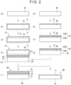
- Fig. 2 is a cross-sectional view showing steps of a production method of the bonded wafer.
- the production method of the bonded wafer includes steps S11 to S14 for producing an active wafer, steps S21 to S25 for producing a handle wafer independently of the active wafer, and steps S31 to S33 for producing the bonded wafer by bonding the active wafer and the handle wafer.
- the steps for producing the active wafer includes an active wafer body preparation step S11, an insulation film growth step S12, an ion implantation layer formation step S13, and a pre-bonding cleaning step S14.
- an active wafer body 10 in a form of a monocrystalline silicon wafer is prepared.
- an insulation film 11 (oxide film) is grown around the active wafer body 10 through, for instance, thermal oxidation, CVD, or the like.
- an ion implantation layer 12 is formed in the active wafer body 10 by implanting hydrogen ion or rare gas ion from above the insulation film 11 using an ion implanter.
- the active layer is cleaned before being bonded in order to remove particles on a bonding surface of the active wafer body 10.
- the active wafer 13 for the bonded wafer is produced through the above steps.
- the steps for producing the handle wafer include a handle wafer body preparation step S21, an oxide film formation step S22, a polycrystalline silicon layer deposition step S23, a polishing step S24, and a pre-bonding cleaning step S25.
- a handle wafer body 20 formed from a monocrystalline silicon wafer is prepared.
- the monocrystalline silicon wafer may be produced by slicing a monocrystalline silicon ingot, which is grown by Czochralski method (CZ method) or floating zone melting method (FZ method), using a wire saw or the like.
- an oxide film 21 (base oxide film) is formed on the handle wafer body 20.
- the thickness of the oxide film 21 is, for instance, in a range from 0.3 nm to 10 nm. With the reduced thickness of the oxide film 21, the oxide film 21 interposed between the handle wafer body 20 and the polycrystalline silicon layer 22 hardly affects properties of the RF device.
- the oxide film 21 may be formed through, for instance, wet cleaning such as alkali cleaning (SC1 cleaning) or acid cleaning (SC2 cleaning).
- the oxide film 21 may be formed by any other method, for example, by thermal oxidation under an oxidative atmosphere or oxidation heat treatment using a rapid heating/cooling device.
- the polycrystalline silicon layer 22 is deposited on the oxide film 21.
- the polycrystalline silicon layer 22 is deposited in two steps including a first growth step for growing a first polycrystalline silicon layer 22A and a second growth step for growing a second polycrystalline silicon layer 22B thicker than the first polycrystalline silicon layer 22A.
- a growth temperature (first temperature) in the first growth step initially performed is in a range from 890 degrees C to 900 degrees C.
- the growth temperature in the first growth step is preferably 895 degrees C.
- a growth temperature (second temperature) in the second growth step performed subsequently to the first growth step is preferably in a range from 1,000 degrees C to 1,075 degrees C, more preferably in a range from 1,050 degrees C to 1,075 degrees C.
- Single crystallization of the polycrystalline silicon layer 22 caused by dissipation of a part of the oxide film 21 can be prevented by forming the oxide film 21 in advance between the surface of the handle wafer body 20 and the polycrystalline silicon layer 22 and by setting the first temperature during the subsequent first growth step in a range from 890 degrees C and 900 degrees C. Further, warpage after polishing can be reduced.
- the second polycrystalline silicon layer 22B is deposited in the second growth step at the second temperature ranging from 1,000 degrees C to 1,075 degrees C to have a thickness larger than that in the first growth step, making it possible to reduce warpage of the handle wafer 23 while the polycrystalline silicon layer 22 is deposited to have a sufficient thickness at efficient high-speed.
- the warpage of the handle wafer 23 can be further reduced by setting the second temperature at 1,050 degrees C or more.
- the warpage of the exemplary embodiment is evaluated in terms of BOW (orientation and dimension of warpage) after polishing.
- BOW which is one of indexes representing the warpage of the entirety of the wafer, is represented by deviation from a center reference plane of a wafer (handle wafer 23) to a median surface at a center point of the wafer.
- the center reference plane of the invention is defined on a basis of best-fit (BOW-bf). Accordingly, a plus (+) BOW-bf value shows convex warpage, whereas a minus (-) BOW-bf value shows concave warpage.
- the warpage may be measured using an optical-sensor type flatness measuring device (Wafercom produced by Lapmaster SFT Corp.) or the like.
- a surface of the polycrystalline silicon layer 22 (the second polycrystalline silicon layer 22B) deposited on the handle wafer body 20 is polished to be flattened.
- the handle wafer 23 for the bonded wafer is produced through the above steps. It should be noted that the steps S11 to S14 and the steps S21 to S25 may be performed in parallel.
- the process for producing the bonded wafer includes a bonding step S31, a peeling heat treatment step S32, and a bonding heat treatment step S33.
- the polished surface of the polycrystalline silicon layer 22 of the handle wafer 23 and the active wafer 13 are bonded through the insulation film 11.
- the active wafer 13 and the handle wafer 23 are bonded so that an implantation surface of the active wafer 13 faces the polycrystalline silicon layer 22.
- the ion implantation layer 12 is subjected to heat treatment (peeling heat treatment) for generating microbubbles to peel the ion implantation layer 12 with the generated microbubbles.
- the bonded wafer 30, in which the insulation film 11 and an active layer 31 are formed on the active wafer 13, is thus produced. It should be noted that a peeled wafer 40 having a peeling surface 41 is also produced.
- the bonded wafer 30 is subjected to bonding heat treatment to enhance the bonding strength at the bonding interface.
- the bonded wafer 30 can be produced as described above.
- the handle wafer 23 used in the above-described production method of the bonded wafer includes the first polycrystalline silicon layer 22A deposited on a side close to the bonding surface of the handle wafer body 20 and the second polycrystalline silicon layer 22B deposited on the first polycrystalline silicon layer 22A.
- the polycrystalline silicon grain size of the polycrystalline silicon layer 22 is 0.419 ⁇ m or less by setting the second temperature (the growth temperature of the second polycrystalline silicon layer 22B) in a range from 1,000 degrees C to 1,075 degrees C.
- the root-mean-square roughness Rq of the polished polycrystalline silicon layer 22 measured in an area of 10 ⁇ m ⁇ 10 ⁇ m is 0.364 nm or less.
- BOW-bf of the bonded wafer 30 is +16 ⁇ m or less.
- the above polycrystalline silicon grain size is a polycrystalline silicon grain size of the second polycrystalline silicon layer 22B.
- the inventors produced the bonded wafer 30 at the growth temperatures shown in Examples, Comparatives, and Reference Examples. Conditions common to Examples, Comparatives, and Reference Examples are shown below.
- the growth temperature for the first growth step was determined after the handle wafer 23 having only the first polycrystalline silicon layer 22A was produced at the growth temperature shown in each of Reference Examples 1 to 3 in Table 1 and the handle wafer 23 and the bonded wafer 30 produced using the handle wafer 23 were evaluated. Specifically, the handle wafer 23 was produced through only one step (i.e., the first step) for growing the first polycrystalline silicon layer 22A in the polycrystalline silicon layer deposition step S23 to perform evaluation. In Reference Example 3, the surface of the wafer was single-crystallized and was not polished, and thus BOW-bf after polishing was not measured. Table 1 Reference Ex. 1 850 degrees C (One Step) Reference Ex. 2 895 degrees C (One Step) Reference Ex.
- the growth temperature in the first growth step was set at 895 degrees C. Further, it was confirmed that the first temperature in a range from 890 degrees C to 900 degrees C was safely applicable.
- the growth temperature for the second growth step was determined after the handle wafer 23 was produced at the growth temperature shown in each of Examples 1 to 4 and Comparatives 1 to 3 in Table 2 and the handle wafer 23 and the bonded wafer 30 produced using the handle wafer 23 were evaluated.
- the handle wafer 23 and the bonded wafer 30 were produced through the production method described with reference to Figs. 1 and 2 .
- the polycrystalline silicon layer 22 was deposited at the deposition temperatures shown in Table 2 (i.e. the first temperature: 895 degrees C, the second temperature: 1,000 degrees C).
- the surface roughness after polishing the polycrystalline silicon layer, the grain size, and BOW-bf of the produced handle wafer 23 were measured.
- the blister defect generated area of the bonded wafer 30 produced with the use of the handle wafer 23 was measured. Furthermore, the presence or absence of slip (a defect along the crystalline surface of silicon) was determined.
- an area of 10 ⁇ m ⁇ 10 ⁇ m of the polished polycrystalline silicon layer 22 was measured with an Atomic Force Microscope (AFM) to calculate the root-mean-square roughness Rq.
- AFM Atomic Force Microscope
- the grain size was measured by an Electron Back Scatter Diffraction Patterns (EBSD) measurement device annexed to a Scanning Electron Microscope (SEM) after polishing.
- EBSD Electron Back Scatter Diffraction Patterns
- SEM Scanning Electron Microscope
- the EBSD measurement which is a crystal analysis process in a form of the application of the principle of Electron Channeling Pattern (ECP) method, allows crystal analysis in a smaller submicron area.
- ECP Electron Channeling Pattern
- the blister defect area was measured using an optical microscope after the wafers were bonded.
- the handle wafer 23 and the bonded wafer 30 were produced as in Example 1. It should be noted that the first and second temperatures were set at the temperatures shown in Table 2 in depositing the polycrystalline silicon layer 22.
- the handle wafer 23 and the bonded wafer 30 were produced as in Examples 1 to 4. It should be noted that the first and second temperatures were set at the temperatures shown in Table 2 in depositing the polycrystalline silicon layer 22.
- Fig. 3 is a graph showing a relationship between the deposition temperature and the blister defect area (horizontal axis: Examples, Comparatives, and Reference Examples (deposition temperature conditions), vertical axis: blister defect area). As shown in Table 1 and Fig. 3 , it is found that the blister defects were correlated with the second temperature, that no blister defects were generated in Examples 1 to 4, and that the blister defects were generated in Comparatives 1 to 3 where the second temperature was 1,080 degrees C or more. Comparatives 1 to 3 reveal that the blister defect area is larger as the second temperature increases.
- the deposition temperature condition for inhibiting the blister defects is 895 degrees C for the first temperature and 1,000 degrees C or more and 1,075 degrees C or less for the second temperature.
- causes of the blister defects include BOW-bf of the handle wafer 23 and the root-mean-square roughness Rq of the polycrystalline silicon layer 22. Since BOW-bf is equal to or less than +35.0 ⁇ m (i.e. acceptable value of BOW-bf) in all of Examples and Comparatives, the cause of the blister defects is believed to be the root-mean-square roughness Rq. Accordingly, the bonded wafer 30 that is not likely to have blister defects is producible by setting the root-mean-square roughness Rq at 0.364 nm or less in view of Table 2.
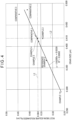
- Fig. 4 is a graph showing a relationship between the grain size and the root-mean-square roughness Rq (horizontal axis: grain size, vertical axis: root-mean-square roughness Rq) of Examples, Comparatives, and Reference Example.
- a blister defect generation threshold (0.364 nm) of the root-mean-square roughness Rq is shown by a chain line L1 in Fig. 4 .
- Fig. 4 shows that the root-mean-square roughness Rq and the grain size are correlated.
- a regression line can be determined based on plotted results of Examples, Comparatives, and Reference Example through the method of least squares. Assuming that the grain size is x and the root-mean-square roughness Rq is y, the regression line can be represented by Formula (1) below. The regression line is shown as a straight line in Fig. 4 .
- y 0.8205 x + 0.0228
- a blister defect generation threshold (0.419 ⁇ m) of the grain size is shown by a chain line L2 in Fig. 4 .
- the results show that BOW-bf is smaller as the second temperature is higher.
- the bonded wafer can have a further reduced BOW-bf by setting the second temperature at 1,050 degrees C or more.
- the bonded wafer 30 can have a BOW-bf of +16 ⁇ m or less by performing the polycrystalline silicon layer deposition step S23 in two steps.
- the development of blister defects can be inhibited by setting the second temperature in a range from 1,000 degrees C to 1,075 degrees C in the production method of the handle wafer for the bonded wafer.
Landscapes
- Recrystallisation Techniques (AREA)
- Crystals, And After-Treatments Of Crystals (AREA)
Abstract
Description
- The present invention relates to a handle wafer used for a bonded wafer produced by bonding an active wafer and the handle wafer.
- Silicon On Insulator (SOI) wafers have been used as substrates for high-frequency (RF: Radio Frequency) devices. The SOI wafers include an insulation film made of, for instance, silicon oxide (SiO2) and an active layer (e.g. monocrystalline silicon), which are sequentially layered on a handle wafer (e.g. monocrystalline silicon wafer).
- One of typical methods for producing the SOI wafers is a bonding method. In the bonding method, the insulation film is formed on at least one of the handle wafer or the active wafer, and then these wafers are bonded through the insulation film. After that, the bonded wafer is subjected to heat treatment at a high temperature of approximately 1,200 degrees C to produce the SOI wafer (hereinafter, the SOI wafer produced by the bonding method will be referred to as a "bonded wafer").
- In order to address RF in the bonded wafer, an increase in resistivity of the handle wafer has been performed (e.g. resistivity of 3000 Ω·cm or more). However, there is a demand for bonded wafers corresponding to higher frequency in response to the need for higher-speed devices, and only increasing the resistivity of the handle wafer becomes insufficient to meet the demand.
- In view of the above, it has been proposed to provide, on a surface of the handle wafer, a polycrystalline silicon layer as a carrier trap layer that traps and annihilates carriers generated during a high-frequency operation (see, for instance, Patent Literature 1). In order to prevent epitaxial growth of silicon on the monocrystalline silicon of the handle wafer, an ultra-thin oxide film is formed on the handle wafer and polycrystalline silicon is formed on the ultra-thin oxide film. A surface provided with the polycrystalline silicon is polished and then bonded with an insulation film formed on the active layer.
- Further,
Patent Literature 1 discloses a two-step growth method of the polycrystalline silicon layer in order to prevent an increase in warpage of the bonded wafer that may otherwise be caused by the thickness of the polycrystalline silicon layer, and partial dissipation of the ultra-thin oxide film due to a high growth temperature and consequent epitaxial growth. According to the above method, the polycrystalline silicon layer is deposited in two steps including a first growth step of growing a first polycrystalline silicon layer and a second growth step of growing a second polycrystalline silicon layer thicker than the first polycrystalline silicon layer. - Patent Literature 1:
JP 2015-211061 A - However, when a surface of the bonded wafer produced as above is observed with an optical microscope or the like, microprojections having a diameter ranging from several tens of micrometers to several millimeters, which swell like blisters, are often seen on a part of the surface of the wafer. These are called blister defects, which are formed because the wafers are not suitably bonded at a bonding interface. The blister defects cause various problems. For instance, the blister defects cause malfunction on a device formed at the part with the defects. Further, a part of the active layer that is positioned on the defects is liable to be peeled to be a dust source during the device production process.
- Presumably, causes of failure in suitably bonding the wafers at the bonding interface are warpage of the handle wafer and surface roughness of the surface of the polycrystalline silicon layer. When the polycrystalline silicon layer is formed by the method disclosed in
Patent Literature 1, the warpage of the handle wafer is restrained. It is thus believed that the blister defects are caused by the surface roughness after surface polishing. - An object of the invention is to provide a handle wafer for a bonded wafer capable of inhibiting development of the blister defects when the bonded wafer is produced.
- A handle wafer according to an aspect of the invention, which is used for a bonded wafer produced by bonding an active wafer and the handle wafer through an insulation film, includes: a handle wafer body; and a polycrystalline silicon layer deposited on a side close to a bonding surface of the handle wafer body, in which the polycrystalline silicon layer has a polycrystalline silicon grain size of 0.419 µm or less.
- In the handle wafer for a bonded wafer according to the above aspect of the invention, a root-mean-square roughness Rq of the polycrystalline silicon layer measured in an area of 10 µm × 10 µm is optionally 0.364 nm or less after the polycrystalline silicon layer is polished.
- In the handle wafer for a bonded wafer according to the above aspect of the invention, the polycrystalline silicon layer is polished and BOW-bf indicating deviation from a center reference plane of the handle wafer to a median surface at a center point of the handle wafer is optionally +16 µm or less.
- In the handle wafer for a bonded wafer according to the above aspect of the invention, the polycrystalline silicon layer optionally includes a first polycrystalline silicon layer deposited on the side close to the bonding surface of the handle wafer body and a second polycrystalline silicon layer deposited on the first polycrystalline silicon layer, and the polycrystalline silicon grain size is optionally a polycrystalline silicon grain size of the second polycrystalline silicon layer.
- The handle wafer body is optionally a monocrystalline silicon wafer.
- According to the above aspect of the invention, development of blister defects can be inhibited when a bonded wafer is produced.
-
-
Fig. 1 is a flow chart for illustrating a process for producing a bonded wafer according to an exemplary embodiment of the invention. -
Fig. 2 is a cross-sectional view showing steps of a production method of the bonded wafer according to the exemplary embodiment of the invention. -
Fig. 3 is a graph showing a relationship between a deposition temperature and a blister defect area of a polycrystalline silicon layer. -
Fig. 4 is a graph showing a relationship between a grain size and a root-mean-square roughness. - Suitable exemplary embodiments of the invention will be described in detail below with reference to the attached drawings. A handle wafer for a bonded wafer of the invention is, for instance, used for a bonded wafer (e.g. the SOI wafer), which is obtained by bonding the handle wafer to an insulation film formed on an active wafer.
- Inventors of the invention have made dedicated studies on the handle wafer for the bonded wafer capable of inhibiting the development of blister defects. As a result, the inventors have found a range of the surface roughness (root-mean-square roughness Rq, RMS) of a polycrystalline silicon layer that may inhibit the development of blister defects. Further, the inventors have found a correlation between the surface roughness and a polycrystalline silicon grain size of the polycrystalline silicon layer, thereby reaching the invention.
-
Fig. 1 is a flowchart for illustrating a process for producing the bonded wafer of the exemplary embodiment.Fig. 2 is a cross-sectional view showing steps of a production method of the bonded wafer. - As shown in
Figs. 1 and2 , the production method of the bonded wafer includes steps S11 to S14 for producing an active wafer, steps S21 to S25 for producing a handle wafer independently of the active wafer, and steps S31 to S33 for producing the bonded wafer by bonding the active wafer and the handle wafer. - The steps for producing the active wafer includes an active wafer body preparation step S11, an insulation film growth step S12, an ion implantation layer formation step S13, and a pre-bonding cleaning step S14.
- In the active wafer body preparation step S11, an
active wafer body 10 in a form of a monocrystalline silicon wafer is prepared. - In the insulation film growth step S12, an insulation film 11 (oxide film) is grown around the
active wafer body 10 through, for instance, thermal oxidation, CVD, or the like. - In the ion implantation layer formation step S13, an
ion implantation layer 12 is formed in theactive wafer body 10 by implanting hydrogen ion or rare gas ion from above theinsulation film 11 using an ion implanter. - In the pre-bonding cleaning step S14, the active layer is cleaned before being bonded in order to remove particles on a bonding surface of the
active wafer body 10. - The
active wafer 13 for the bonded wafer is produced through the above steps. - The steps for producing the handle wafer include a handle wafer body preparation step S21, an oxide film formation step S22, a polycrystalline silicon layer deposition step S23, a polishing step S24, and a pre-bonding cleaning step S25.
- In the handle wafer body preparation step S21, a
handle wafer body 20 formed from a monocrystalline silicon wafer is prepared. The monocrystalline silicon wafer may be produced by slicing a monocrystalline silicon ingot, which is grown by Czochralski method (CZ method) or floating zone melting method (FZ method), using a wire saw or the like. - In the oxide film formation step S22, an oxide film 21 (base oxide film) is formed on the
handle wafer body 20. Preferably, the thickness of theoxide film 21 is, for instance, in a range from 0.3 nm to 10 nm. With the reduced thickness of theoxide film 21, theoxide film 21 interposed between thehandle wafer body 20 and thepolycrystalline silicon layer 22 hardly affects properties of the RF device. - The
oxide film 21 may be formed through, for instance, wet cleaning such as alkali cleaning (SC1 cleaning) or acid cleaning (SC2 cleaning). Theoxide film 21 may be formed by any other method, for example, by thermal oxidation under an oxidative atmosphere or oxidation heat treatment using a rapid heating/cooling device. - In the polycrystalline silicon layer deposition step S23, the
polycrystalline silicon layer 22 is deposited on theoxide film 21. Thepolycrystalline silicon layer 22 is deposited in two steps including a first growth step for growing a firstpolycrystalline silicon layer 22A and a second growth step for growing a secondpolycrystalline silicon layer 22B thicker than the firstpolycrystalline silicon layer 22A. - A growth temperature (first temperature) in the first growth step initially performed is in a range from 890 degrees C to 900 degrees C. The growth temperature in the first growth step is preferably 895 degrees C.
- A growth temperature (second temperature) in the second growth step performed subsequently to the first growth step is preferably in a range from 1,000 degrees C to 1,075 degrees C, more preferably in a range from 1,050 degrees C to 1,075 degrees C.
- Single crystallization of the
polycrystalline silicon layer 22 caused by dissipation of a part of theoxide film 21 can be prevented by forming theoxide film 21 in advance between the surface of thehandle wafer body 20 and thepolycrystalline silicon layer 22 and by setting the first temperature during the subsequent first growth step in a range from 890 degrees C and 900 degrees C. Further, warpage after polishing can be reduced. - The second
polycrystalline silicon layer 22B is deposited in the second growth step at the second temperature ranging from 1,000 degrees C to 1,075 degrees C to have a thickness larger than that in the first growth step, making it possible to reduce warpage of thehandle wafer 23 while thepolycrystalline silicon layer 22 is deposited to have a sufficient thickness at efficient high-speed. The warpage of thehandle wafer 23 can be further reduced by setting the second temperature at 1,050 degrees C or more. - The warpage of the exemplary embodiment is evaluated in terms of BOW (orientation and dimension of warpage) after polishing. BOW, which is one of indexes representing the warpage of the entirety of the wafer, is represented by deviation from a center reference plane of a wafer (handle wafer 23) to a median surface at a center point of the wafer. The center reference plane of the invention is defined on a basis of best-fit (BOW-bf). Accordingly, a plus (+) BOW-bf value shows convex warpage, whereas a minus (-) BOW-bf value shows concave warpage. For instance, the warpage may be measured using an optical-sensor type flatness measuring device (Wafercom produced by Lapmaster SFT Corp.) or the like.
- In the polishing step S24, a surface of the polycrystalline silicon layer 22 (the second
polycrystalline silicon layer 22B) deposited on thehandle wafer body 20 is polished to be flattened. - In the pre-bonding cleaning step S25, particles on the polished surface of the
polycrystalline silicon layer 22 are removed. - The
handle wafer 23 for the bonded wafer is produced through the above steps. It should be noted that the steps S11 to S14 and the steps S21 to S25 may be performed in parallel. - Next, a process for bonding the
active wafer 13 and thehandle wafer 23 to produce a bondedwafer 30 will be described below. - The process for producing the bonded wafer includes a bonding step S31, a peeling heat treatment step S32, and a bonding heat treatment step S33.
- In the bonding step S31, the polished surface of the
polycrystalline silicon layer 22 of thehandle wafer 23 and theactive wafer 13 are bonded through theinsulation film 11. At this time, theactive wafer 13 and thehandle wafer 23 are bonded so that an implantation surface of theactive wafer 13 faces thepolycrystalline silicon layer 22. - In the peeling heat treatment step S32, the
ion implantation layer 12 is subjected to heat treatment (peeling heat treatment) for generating microbubbles to peel theion implantation layer 12 with the generated microbubbles. The bondedwafer 30, in which theinsulation film 11 and anactive layer 31 are formed on theactive wafer 13, is thus produced. It should be noted that a peeledwafer 40 having a peelingsurface 41 is also produced. - In the bonding heat treatment step S33, the bonded
wafer 30 is subjected to bonding heat treatment to enhance the bonding strength at the bonding interface. - The bonded
wafer 30 can be produced as described above. - The
handle wafer 23 used in the above-described production method of the bonded wafer includes the firstpolycrystalline silicon layer 22A deposited on a side close to the bonding surface of thehandle wafer body 20 and the secondpolycrystalline silicon layer 22B deposited on the firstpolycrystalline silicon layer 22A. Further, the polycrystalline silicon grain size of thepolycrystalline silicon layer 22 is 0.419 µm or less by setting the second temperature (the growth temperature of the secondpolycrystalline silicon layer 22B) in a range from 1,000 degrees C to 1,075 degrees C. Furthermore, the root-mean-square roughness Rq of the polishedpolycrystalline silicon layer 22 measured in an area of 10 µm × 10 µm is 0.364 nm or less. Moreover, BOW-bf of the bondedwafer 30 is +16 µm or less. The above polycrystalline silicon grain size is a polycrystalline silicon grain size of the secondpolycrystalline silicon layer 22B. - The development of the blister defects is inhibited in the bonded
wafer 30 produced with the use of thehandle wafer 23 that satisfies the above requirements. Examples - In order to determine the growth temperature in depositing the
polycrystalline silicon layer 22, the inventors produced the bondedwafer 30 at the growth temperatures shown in Examples, Comparatives, and Reference Examples. Conditions common to Examples, Comparatives, and Reference Examples are shown below. -
- Diameter of handle wafer: 200 mm
- Crystal orientation of handle wafer: <100>
- Resistivity of handle wafer: 12,060 Ω·cm
- Oxygen concentration of handle wafer: 2.99 × 10¹⁷ atoms/cm3
- Base oxide film formation: SC1 cleaning; Oxide film thickness approximately 1 nm
- BOX oxidation: 1,050 degrees C; Oxide film thickness 400 nm
- Hydrogen ion implantation: 105 keV
- Peeling heat treatment: 500 degrees C; 30 minutes; 100% Ar atmosphere
- Bonding heat treatment: 900 degrees C pyrogenic oxidation + Ar annealing at 1,100 degrees C for 120 minutes.
- Initially, the growth temperature for the first growth step (first temperature) was determined after the
handle wafer 23 having only the firstpolycrystalline silicon layer 22A was produced at the growth temperature shown in each of Reference Examples 1 to 3 in Table 1 and thehandle wafer 23 and the bondedwafer 30 produced using thehandle wafer 23 were evaluated. Specifically, thehandle wafer 23 was produced through only one step (i.e., the first step) for growing the firstpolycrystalline silicon layer 22A in the polycrystalline silicon layer deposition step S23 to perform evaluation. In Reference Example 3, the surface of the wafer was single-crystallized and was not polished, and thus BOW-bf after polishing was not measured.Table 1 Reference Ex. 1 850 degrees C (One Step) Reference Ex. 2 895 degrees C (One Step) Reference Ex. 3 950 degrees C (One Step) Fist Temperature (degrees C) 850 895 950 Thickness of First Layer (µm) 2.25 2.25 2.25 Growth Rate (µm/min.) 0.12 0.28 0.59 BOW-bf (µm) +49.3 +31.4 - Crystalline State Polycrystal Polycrystal Monocrystal - As a result of the evaluation, it was found that BOW of the
handle wafer 23 was large at the first temperature of 850 degrees C. Further, it was found that a part of theoxide film 21 on the surface of thehandle wafer 23 was dissipated and the part was single-crystallized at the first temperature of 950 degrees C. In view of the above, the growth temperature in the first growth step was set at 895 degrees C. Further, it was confirmed that the first temperature in a range from 890 degrees C to 900 degrees C was safely applicable. - Subsequently, the growth temperature for the second growth step (second temperature) was determined after the
handle wafer 23 was produced at the growth temperature shown in each of Examples 1 to 4 andComparatives 1 to 3 in Table 2 and thehandle wafer 23 and the bondedwafer 30 produced using thehandle wafer 23 were evaluated.Table 2 Reference Ex. 2 895 degrees C (One Step) Ex. 1 895/1,000 degrees C (Two Steps) Ex. 2 895/1,050 degrees C (Two Steps) Ex. 3 895/1,070 degrees C (Two Steps) Ex. 4 895/1,075 degrees C (Two Steps) Comp. 1 895/1,080 degrees C (Two Steps) Comp. 2 895/1,100 degrees C (Two Steps) Comp. 3 895/1,150 degrees C (Two Steps) First Temperature (degrees C) 895 895 895 895 895 895 895 895 Second Temperature (degrees C) - 1,000 1,050 1,070 1,075 1,080 1,100 1,150 Growth Rate (µm/min.) 0.280 0.687 0.775 0.794 0.799 0.809 0.814 0.930 Root-Mean-Square Roughness Rq (nm) 0.327 0.269 0.342 0.360 0.364 0.371 0.408 0.443 Grain Size (µm) 0.367 0.293 0.418 0.412 0.419 0.424 0.485 0.475 Blister Defects Generated Area (mm2) 0 0 0 0 0 39 161 277 Thickness of First Layer (µm) 2.25 0.3 0.3 0.3 0.3 0.3 0.3 0.3 Thickness of Second Layer (µm) - 1.95 1.95 1.95 1.95 1.95 1.95 1.95 Slip Determination Results Passed Passed Passed Passed Passed Failed Failed Failed BOW-bf (µm) +31.4 +15.6 +9.2 +7.3 +6.6 +6.3 +2.5 +0.6 - The
handle wafer 23 and the bondedwafer 30 were produced through the production method described with reference toFigs. 1 and2 . In Example 1, thepolycrystalline silicon layer 22 was deposited at the deposition temperatures shown in Table 2 (i.e. the first temperature: 895 degrees C, the second temperature: 1,000 degrees C). - The surface roughness after polishing the polycrystalline silicon layer, the grain size, and BOW-bf of the produced
handle wafer 23 were measured. - Further, the blister defect generated area of the bonded
wafer 30 produced with the use of thehandle wafer 23 was measured. Furthermore, the presence or absence of slip (a defect along the crystalline surface of silicon) was determined. - In order to determine the surface roughness, an area of 10 µm ×10 µm of the polished
polycrystalline silicon layer 22 was measured with an Atomic Force Microscope (AFM) to calculate the root-mean-square roughness Rq. - The grain size was measured by an Electron Back Scatter Diffraction Patterns (EBSD) measurement device annexed to a Scanning Electron Microscope (SEM) after polishing. The EBSD measurement, which is a crystal analysis process in a form of the application of the principle of Electron Channeling Pattern (ECP) method, allows crystal analysis in a smaller submicron area. The grain size is calculated from a pattern obtained at the time of electron irradiation.
- The blister defect area was measured using an optical microscope after the wafers were bonded.
- The
handle wafer 23 and the bondedwafer 30 were produced as in Example 1. It should be noted that the first and second temperatures were set at the temperatures shown in Table 2 in depositing thepolycrystalline silicon layer 22. - The
handle wafer 23 and the bondedwafer 30 were produced as in Examples 1 to 4. It should be noted that the first and second temperatures were set at the temperatures shown in Table 2 in depositing thepolycrystalline silicon layer 22. -
Fig. 3 is a graph showing a relationship between the deposition temperature and the blister defect area (horizontal axis: Examples, Comparatives, and Reference Examples (deposition temperature conditions), vertical axis: blister defect area). As shown in Table 1 andFig. 3 , it is found that the blister defects were correlated with the second temperature, that no blister defects were generated in Examples 1 to 4, and that the blister defects were generated inComparatives 1 to 3 where the second temperature was 1,080 degrees C or more.Comparatives 1 to 3 reveal that the blister defect area is larger as the second temperature increases. - Based on the results, it is determined that the deposition temperature condition for inhibiting the blister defects is 895 degrees C for the first temperature and 1,000 degrees C or more and 1,075 degrees C or less for the second temperature.
- Assumingly, causes of the blister defects include BOW-bf of the
handle wafer 23 and the root-mean-square roughness Rq of thepolycrystalline silicon layer 22. Since BOW-bf is equal to or less than +35.0 µm (i.e. acceptable value of BOW-bf) in all of Examples and Comparatives, the cause of the blister defects is believed to be the root-mean-square roughness Rq. Accordingly, the bondedwafer 30 that is not likely to have blister defects is producible by setting the root-mean-square roughness Rq at 0.364 nm or less in view of Table 2. -
Fig. 4 is a graph showing a relationship between the grain size and the root-mean-square roughness Rq (horizontal axis: grain size, vertical axis: root-mean-square roughness Rq) of Examples, Comparatives, and Reference Example. A blister defect generation threshold (0.364 nm) of the root-mean-square roughness Rq is shown by a chain line L1 inFig. 4 . -
Fig. 4 shows that the root-mean-square roughness Rq and the grain size are correlated. Specifically, a regression line can be determined based on plotted results of Examples, Comparatives, and Reference Example through the method of least squares. Assuming that the grain size is x and the root-mean-square roughness Rq is y, the regression line can be represented by Formula (1) below. The regression line is shown as a straight line inFig. 4 . A determination coefficient of the regression line is R2 = 0.9092.
- Based on the correlation, it is found that the blister defects can be inhibited also by setting the grain size at 0.419 µm or less. A blister defect generation threshold (0.419 µm) of the grain size is shown by a chain line L2 in
Fig. 4 . - In regard to the presence or absence of slip, the results of cases where the second temperature was 1,080 degrees C or more (
Comparatives 1 to 3) were unfavorable (failed). Assumingly, the high deposition temperature of thepolycrystalline silicon layer 22 is a cause of the occurrence of slip defects. - In regard to the BOW-bf after polishing, the results show that BOW-bf is smaller as the second temperature is higher. In Examples 1 to 4, the case where the second temperature was 1,000 degrees C had the largest value (15.6 µm). However, since no blister defects were generated at the value, it is believed that no problem is caused provided that that BOW-bf is +16 µm or less. Further, the bonded wafer can have a further reduced BOW-bf by setting the second temperature at 1,050 degrees C or more.
- In view of the above, it is found that the development of blister defects can be inhibited by setting the polycrystalline silicon grain size of the
polycrystalline silicon layer 22 at 0.419 µm or less in thehandle wafer 23 for the bonded wafer having thepolycrystalline silicon layer 22. - Similarly, it is found that the development of blister defects can be inhibited by setting the root-mean-square roughness Rq of the polished
polycrystalline silicon layer 22 at 0.364 nm or less. - It is also found that the bonded
wafer 30 can have a BOW-bf of +16 µm or less by performing the polycrystalline silicon layer deposition step S23 in two steps. - It is further found that the development of blister defects can be inhibited by setting the second temperature in a range from 1,000 degrees C to 1,075 degrees C in the production method of the handle wafer for the bonded wafer.
- 10...active wafer body, 11...insulation film, 12... ion implantation layer, 13...active wafer, 20...handle wafer body, 21...oxide film, 22...polycrystalline silicon layer, 22A...first polycrystalline silicon layer, 22B...second polycrystalline silicon layer, 23...handle wafer, 30...bonded wafer, 31...active layer, 40...peeled wafer, 41 ... peeling surface
Claims (5)
- A handle wafer used for a bonded wafer produced by bonding an active wafer and the handle wafer through an insulation film, the handle wafer comprising:a handle wafer body; anda polycrystalline silicon layer deposited on a side close to a bonding surface of the handle wafer body, whereinthe polycrystalline silicon layer has a polycrystalline silicon grain size of 0.419 µm or less.
- The handle wafer for a bonded wafer according to claim 1, wherein a root-mean-square roughness Rq of the polycrystalline silicon layer measured in an area of 10 µm × 10 µm is 0.364 nm or less after the polycrystalline silicon layer is polished.
- The handle wafer for a bonded wafer according to claim 1 or 2, wherein the polycrystalline silicon layer is polished and BOW-bf indicating deviation from a center reference plane of the handle wafer to a median surface at a center point of the handle wafer is +16 µm or less.
- The handle wafer for a bonded wafer according to any one of claims 1 to 3, wherein the polycrystalline silicon layer comprises a first polycrystalline silicon layer deposited on the side close to the bonding surface of the handle wafer body and a second polycrystalline silicon layer deposited on the first polycrystalline silicon layer, and
the polycrystalline silicon grain size is a polycrystalline silicon grain size of the second polycrystalline silicon layer. - The handle wafer for a bonded wafer according to any one of claims 1 to 4, wherein the handle wafer body is a monocrystalline silicon wafer.
Applications Claiming Priority (2)
| Application Number | Priority Date | Filing Date | Title |
|---|---|---|---|
| JP2020097711A JP2021190660A (en) | 2020-06-04 | 2020-06-04 | Support substrate for bonded wafers |
| PCT/JP2021/020199 WO2021246279A1 (en) | 2020-06-04 | 2021-05-27 | Support substrate for bonded wafer |
Publications (2)
| Publication Number | Publication Date |
|---|---|
| EP4163954A1 true EP4163954A1 (en) | 2023-04-12 |
| EP4163954A4 EP4163954A4 (en) | 2024-07-10 |
Family
ID=78831126
Family Applications (1)
| Application Number | Title | Priority Date | Filing Date |
|---|---|---|---|
| EP21818434.9A Withdrawn EP4163954A4 (en) | 2020-06-04 | 2021-05-27 | CARRIER SUBSTRATE FOR BONDED WAFERS |
Country Status (6)
| Country | Link |
|---|---|
| US (1) | US20230230875A1 (en) |
| EP (1) | EP4163954A4 (en) |
| JP (1) | JP2021190660A (en) |
| KR (1) | KR20230005360A (en) |
| CN (1) | CN115668449A (en) |
| WO (1) | WO2021246279A1 (en) |
Families Citing this family (1)
| Publication number | Priority date | Publication date | Assignee | Title |
|---|---|---|---|---|
| JP7529000B2 (en) * | 2022-11-15 | 2024-08-06 | 株式会社Sumco | Manufacturing method of laminated wafer |
Family Cites Families (13)
| Publication number | Priority date | Publication date | Assignee | Title |
|---|---|---|---|---|
| JP2000138194A (en) * | 1998-08-28 | 2000-05-16 | Sony Corp | Method for polishing semiconductor substrate and method for manufacturing bonded semiconductor substrate |
| JP2004320050A (en) * | 2004-06-29 | 2004-11-11 | Sumitomo Mitsubishi Silicon Corp | Soi substrate and method for manufacturing same |
| JP5532527B2 (en) * | 2006-08-03 | 2014-06-25 | 株式会社デンソー | SOI substrate and manufacturing method thereof |
| JP2009252948A (en) * | 2008-04-04 | 2009-10-29 | Sumco Corp | Method of manufacturing stuck wafer |
| FR3019373A1 (en) * | 2014-03-31 | 2015-10-02 | St Microelectronics Sa | METHOD FOR MANUFACTURING SEMICONDUCTOR PLATE ADAPTED FOR MANUFACTURING SOI SUBSTRATE AND SUBSTRATE PLATE THUS OBTAINED |
| JP6118757B2 (en) * | 2014-04-24 | 2017-04-19 | 信越半導体株式会社 | Manufacturing method of bonded SOI wafer |
| JP6100200B2 (en) | 2014-04-24 | 2017-03-22 | 信越半導体株式会社 | Manufacturing method of bonded SOI wafer |
| EP3266038B1 (en) * | 2015-03-03 | 2019-09-25 | GlobalWafers Co., Ltd. | Method of depositing charge trapping polycrystalline silicon films on silicon substrates with controllable film stress |
| FR3048306B1 (en) * | 2016-02-26 | 2018-03-16 | Soitec | SUPPORT FOR A SEMICONDUCTOR STRUCTURE |
| JP6443394B2 (en) * | 2016-06-06 | 2018-12-26 | 信越半導体株式会社 | Manufacturing method of bonded SOI wafer |
| JP6498635B2 (en) * | 2016-06-23 | 2019-04-10 | 信越半導体株式会社 | Manufacturing method of bonded SOI wafer |
| US11063117B2 (en) * | 2017-04-20 | 2021-07-13 | Taiwan Semiconductor Manufacturing Co., Ltd. | Semiconductor device structure having carrier-trapping layers with different grain sizes |
| JP6827442B2 (en) * | 2018-06-14 | 2021-02-10 | 信越半導体株式会社 | Manufacturing method of bonded SOI wafer and bonded SOI wafer |
-
2020
- 2020-06-04 JP JP2020097711A patent/JP2021190660A/en active Pending
-
2021
- 2021-05-27 EP EP21818434.9A patent/EP4163954A4/en not_active Withdrawn
- 2021-05-27 WO PCT/JP2021/020199 patent/WO2021246279A1/en not_active Ceased
- 2021-05-27 KR KR1020227042388A patent/KR20230005360A/en not_active Ceased
- 2021-05-27 CN CN202180039914.7A patent/CN115668449A/en active Pending
- 2021-05-27 US US18/007,848 patent/US20230230875A1/en not_active Abandoned
Also Published As
| Publication number | Publication date |
|---|---|
| KR20230005360A (en) | 2023-01-09 |
| JP2021190660A (en) | 2021-12-13 |
| WO2021246279A1 (en) | 2021-12-09 |
| CN115668449A (en) | 2023-01-31 |
| EP4163954A4 (en) | 2024-07-10 |
| US20230230875A1 (en) | 2023-07-20 |
Similar Documents
| Publication | Publication Date | Title |
|---|---|---|
| US7763541B2 (en) | Process for regenerating layer transferred wafer | |
| EP3351660B1 (en) | Manufacturing method of sic composite substrate | |
| EP3352197B1 (en) | Method for producing a composite sic substrate | |
| EP3309819B1 (en) | Bonded soi wafer manufacturing method | |
| EP2159826A1 (en) | Soi wafer manufacturing method | |
| EP1758154B1 (en) | Method for producing silicon wafer | |
| US7186628B2 (en) | Method of manufacturing an SOI wafer where COP's are eliminated within the base wafer | |
| EP2187429B1 (en) | Bonding wafer manufacturing method | |
| CN109075028B (en) | Manufacturing method of bonded SOI wafer | |
| US20230230875A1 (en) | Support substrate for bonded wafer | |
| EP3809448A1 (en) | Bonded soi wafer and method for manufacturing bonded soi wafer | |
| KR20120023056A (en) | Silicon wafer and method for producing the same | |
| US20080251879A1 (en) | Method for Manufacturing Simox Substrate and Simox Substrate Obtained by this Method | |
| JP7529000B2 (en) | Manufacturing method of laminated wafer | |
| US12400909B2 (en) | Method for producing support substrate for bonded wafer, and support substrate for bonded wafer | |
| JP2010040638A (en) | Method of manufacturing soi substrate | |
| JP2003197547A (en) | Method of manufacturing silicon epitaxial wafer |
Legal Events
| Date | Code | Title | Description |
|---|---|---|---|
| STAA | Information on the status of an ep patent application or granted ep patent |
Free format text: STATUS: THE INTERNATIONAL PUBLICATION HAS BEEN MADE |
|
| PUAI | Public reference made under article 153(3) epc to a published international application that has entered the european phase |
Free format text: ORIGINAL CODE: 0009012 |
|
| STAA | Information on the status of an ep patent application or granted ep patent |
Free format text: STATUS: REQUEST FOR EXAMINATION WAS MADE |
|
| 17P | Request for examination filed |
Effective date: 20221214 |
|
| AK | Designated contracting states |
Kind code of ref document: A1 Designated state(s): AL AT BE BG CH CY CZ DE DK EE ES FI FR GB GR HR HU IE IS IT LI LT LU LV MC MK MT NL NO PL PT RO RS SE SI SK SM TR |
|
| DAV | Request for validation of the european patent (deleted) | ||
| DAX | Request for extension of the european patent (deleted) | ||
| A4 | Supplementary search report drawn up and despatched |
Effective date: 20240611 |
|
| RIC1 | Information provided on ipc code assigned before grant |
Ipc: H01L 27/12 20060101ALI20240605BHEP Ipc: H01L 21/02 20060101AFI20240605BHEP |
|
| STAA | Information on the status of an ep patent application or granted ep patent |
Free format text: STATUS: THE APPLICATION IS DEEMED TO BE WITHDRAWN |
|
| 18D | Application deemed to be withdrawn |
Effective date: 20250103 |