EP4161226A1 - Emc housing - Google Patents
Emc housing Download PDFInfo
- Publication number
- EP4161226A1 EP4161226A1 EP21200102.8A EP21200102A EP4161226A1 EP 4161226 A1 EP4161226 A1 EP 4161226A1 EP 21200102 A EP21200102 A EP 21200102A EP 4161226 A1 EP4161226 A1 EP 4161226A1
- Authority
- EP
- European Patent Office
- Prior art keywords
- gasket
- emc
- housing according
- interface surface
- regions
- Prior art date
- Legal status (The legal status is an assumption and is not a legal conclusion. Google has not performed a legal analysis and makes no representation as to the accuracy of the status listed.)
- Pending
Links
Images

Classifications
-
- H—ELECTRICITY
- H05—ELECTRIC TECHNIQUES NOT OTHERWISE PROVIDED FOR
- H05K—PRINTED CIRCUITS; CASINGS OR CONSTRUCTIONAL DETAILS OF ELECTRIC APPARATUS; MANUFACTURE OF ASSEMBLAGES OF ELECTRICAL COMPONENTS
- H05K5/00—Casings, cabinets or drawers for electric apparatus
- H05K5/0026—Casings, cabinets or drawers for electric apparatus provided with connectors and printed circuit boards [PCB], e.g. automotive electronic control units
- H05K5/0047—Casings, cabinets or drawers for electric apparatus provided with connectors and printed circuit boards [PCB], e.g. automotive electronic control units having a two-part housing enclosing a PCB
- H05K5/0052—Casings, cabinets or drawers for electric apparatus provided with connectors and printed circuit boards [PCB], e.g. automotive electronic control units having a two-part housing enclosing a PCB characterized by joining features of the housing parts
-
- H—ELECTRICITY
- H05—ELECTRIC TECHNIQUES NOT OTHERWISE PROVIDED FOR
- H05K—PRINTED CIRCUITS; CASINGS OR CONSTRUCTIONAL DETAILS OF ELECTRIC APPARATUS; MANUFACTURE OF ASSEMBLAGES OF ELECTRICAL COMPONENTS
- H05K5/00—Casings, cabinets or drawers for electric apparatus
- H05K5/0026—Casings, cabinets or drawers for electric apparatus provided with connectors and printed circuit boards [PCB], e.g. automotive electronic control units
- H05K5/0047—Casings, cabinets or drawers for electric apparatus provided with connectors and printed circuit boards [PCB], e.g. automotive electronic control units having a two-part housing enclosing a PCB
- H05K5/006—Casings, cabinets or drawers for electric apparatus provided with connectors and printed circuit boards [PCB], e.g. automotive electronic control units having a two-part housing enclosing a PCB characterized by features for holding the PCB within the housing
-
- H—ELECTRICITY
- H05—ELECTRIC TECHNIQUES NOT OTHERWISE PROVIDED FOR
- H05K—PRINTED CIRCUITS; CASINGS OR CONSTRUCTIONAL DETAILS OF ELECTRIC APPARATUS; MANUFACTURE OF ASSEMBLAGES OF ELECTRICAL COMPONENTS
- H05K5/00—Casings, cabinets or drawers for electric apparatus
- H05K5/06—Hermetically-sealed casings
- H05K5/061—Hermetically-sealed casings sealed by a gasket held between a removable cover and a body, e.g. O-ring, packing
-
- H—ELECTRICITY
- H05—ELECTRIC TECHNIQUES NOT OTHERWISE PROVIDED FOR
- H05K—PRINTED CIRCUITS; CASINGS OR CONSTRUCTIONAL DETAILS OF ELECTRIC APPARATUS; MANUFACTURE OF ASSEMBLAGES OF ELECTRICAL COMPONENTS
- H05K9/00—Screening of apparatus or components against electric or magnetic fields
- H05K9/0007—Casings
- H05K9/0009—Casings with provisions to reduce EMI leakage through the joining parts
-
- H—ELECTRICITY
- H05—ELECTRIC TECHNIQUES NOT OTHERWISE PROVIDED FOR
- H05K—PRINTED CIRCUITS; CASINGS OR CONSTRUCTIONAL DETAILS OF ELECTRIC APPARATUS; MANUFACTURE OF ASSEMBLAGES OF ELECTRICAL COMPONENTS
- H05K9/00—Screening of apparatus or components against electric or magnetic fields
- H05K9/0007—Casings
- H05K9/0015—Gaskets or seals
Definitions
- the present disclosure relates to an electromagnetic compatibility (EMC) housing and an automotive electronics housing for electromagnetic interference (EMI) shielding.
- EMC electromagnetic compatibility
- EMI electromagnetic interference
- EMI shielding housings that form an electrically grounded barrier for absorbing electromagnetic radiation.
- Such housings will normally be provided in two separable parts for allowing the housing to be opened during assembly and to facilitate access to the device for subsequent maintenance. Accordingly, a second part of the housing will typically form a removable panel or cover that is secured by screws over the first part, with the parts fitting together at opposing interface surfaces.
- An resilient, electrically conductive EMI shielding gasket will also be provided between the interface surfaces to seal between the faces.
- the shielding gasket In order for the shielding gasket to work effectively, it must be compressed within a specific compression range.
- the interface surfaces rarely mate together perfectly due to inherent manufacturing tolerances, casting defects and thermal differences.
- the stiffness of the cover part is also often not sufficient to properly compress the gasket over the whole of the interface between the parts.
- Figure 1 shows a isometric view of a conventional automotive EMC housing 1 having a base part 2 covered by a cover part 3 for enclosing a printed circuit board (PCB) 6.
- the cover 3 is shown with an exaggerated deformation scaled up by 20 times for illustration.
- the base and cover interface surfaces 4,5 diverge from one another in a number of areas, resulting in gaps in the enclosure. In these areas, the gasket provided between the interface surfaces may not be sufficiently compressed to within the desired compression range to form an effective EMI shield. As such, electromagnetic radiation may leak through or be emitted from the housing in these areas.
- the EMI shielding cannot be improved by further tightening the screw fixings securing the cover part 3 to the base part 2 because, although this helps to compress the parts together, its effectiveness is limited by the stiffness of the cover 3 and it also leads to higher forces being applied to the PCB 6. Accordingly, the loading across the PCB 6 can result in strains across the electronic components and interconnects, and ultimately have the potential to result in component failure or reliability issues.
- an electromagnetic compatibility, EMC, housing including: a first part and a second part for forming an enclosure when fitted together, wherein the first and second parts include first and second interface surfaces, respectively, for compressing a gasket interposed between the interface surfaces when the first and second parts are fitted together, and wherein at least one of the first and second interface surfaces includes a plurality of undercut regions for reducing compression of the gasket in the region when the first and second parts are fitted together.
- the forces required to compress the gasket as a whole are reduced. At the same time, this may be achieved without needing to modify the gasket itself. Consequently, the gasket may be sufficiently compressed to achieve the required EMI shielding effect over its whole length, but without imposing excessive strain on the electronic components housed therein. As such, electromagnetic compatibility may be achieved, without increasing manufacturing or production costs.
- the undercut regions are between 40-60% of the respective interface surface. In this way, the required forces to achieve sufficient compression for EMI shielding may be reduced by a proportionate amount.
- the plurality of undercut regions form a pattern of undulations in the respective interface surface. In this way, a more uniform compression level may be achieved throughout the interface surfaces as a whole.
- undercut regions are interspersed between projecting regions of the respective interface surface.
- spacing between the projecting regions is between 5-20mm, where the spacing defines undercut regions. In embodiments, the spacing between the projecting regions is between 6-14mm.
- the projecting regions are between 5-20mm long. In embodiments, the projecting regions are between 6-14mm long.
- the EMC housing further includes the gasket.
- the gasket includes an electrically conductive elastomer material.
- the gasket is deposited onto the first interface surface. In embodiments, a section of the gasket is dispensed onto the first interface surface.
- the first interface surface is for compressing the gasket against the second interface surface when the first and second parts are fitted together.
- the first interface surface is for compressing the gasket against a circuit board interposed between the interface surfaces when the first and second parts are fitted together.
- the gasket or a section of a gasket may form a resilient support for supporting a circuit board.
- the EMC housing further includes a further gasket.
- the second interface surface is for compressing the further gasket against a circuit board interposed between the interface surfaces when the first and second parts are fitted together.
- the gasket is an Electromagnetic Interference, EMI, shielding gasket.
- the housing is an automotive electronics housing.
- the first part and the second part are configured to form an enclosure around an automotive electronic control unit when fitted together.
- the automotive EMC housing includes a base part 2 and a cover part 3 that are fitted together, with a gasket 9 interposed between, to form an assembled EMC housing.
- Figure 2 shows a isometric view of the base part 2 of the automotive EMC housing according to the illustrative embodiment.
- the base part 2 includes a first interface surface 4 which mates with a corresponding second interface surface 5 on the cover part 3, when the base and cover are fitted together.
- the first interface surface 4 includes two side sections 4a extending along the sides of the housing, and two end sections 4b extending along the ends of the housing.
- both side and end sections of the first interface surface have a shaped surface profile in the form of flattened undulations extending along their lengths.
- these undulations are visible in the side interface surface sections 4a as projecting regions 8 interspersed with undercut regions 7.
- Corresponding undulations are formed on the end interface surface sections 4b, albeit that this is less visible in Figure 2 because a second gasket section 9b has been deposited over them.
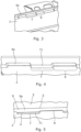
- Figures 3 and 4 respectively show enlarged isometric and side views of one of the interface surfaces.
- the interface surface has an undulating profile with the flattened bases of undercut regions 7 being in a different plane to the plane of the flattened tops of the projecting regions 8. As such, a repeating pattern of projections and undercuts is provided, with spaces 71 being defined by the undercut regions 7, between the planes of these formations.
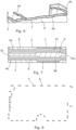
- Figure 5 shows an enlarged isometric view of a side interface surface section 4a and gasket 9 in the assembled EMC housing.
- the gasket 9 is formed as a elongate body of electrically conductive elastomer material, and the projecting regions 8 form a seat onto which the gasket 9 is seated.
- the spaces 71 formed by undercuts 7 provide an area for the adjacent regions of the gasket 9 to be moved into when the assembly is compressed.
- the side sections of the second interface surface 5 provided on the cover part 3 have a flat surface which is used to press the gasket 9 into the first interface surface 4.
- the projecting regions 8 of the first interface surface 4 will project into the gasket material when the base part 2 and cover part 3 are brought together by the screw fixtures.
- the gasket material will contact the surface of the undercut regions 7, the gasket material in these regions will be substantially uncompressed due to the space 71.
- Figure 6 shows an enlarged isometric view of an end interface surface section 4b of the base part 2, which forms an elastic support for the PCB 6.
- the end interface surface sections 4b have corresponding undulations to those provided in the side interface surface sections 4a, with the same repeating pattern of undercuts 7 and projecting regions 8.
- a second section of the gasket 9b is deposited directly onto the interface surface 4 of the base part 2, and forms a lower compressible support for the PCB 6.
- the second section of the gasket 9b adopts a corresponding undulating profile to the interface surface 4 onto which it is deposited, with the gasket 9b protruding in regions over the projecting regions 8 of the interface surface 4, and being recessed in in regions over the undercut regions 7 of the interface surface 4.
- the end sections of the second interface surface 5 provided on the cover part 3 also have a corresponding undulated profile to that provided on the end sections of the first interface surface 4b shown in Figure 6 . That is, in contrast to the flat side sections of the second interface surface 5, the end sections of this surface are provided with a pattern of projecting regions 8 and undercut regions 7. At the same time, a second gasket 10 is also deposited directly onto this second interface surface 5 to produce a corresponding undulating profile for forming an upper compressible support for the PCB 6.
- the end sections of the first and second interface surfaces 4,5 therefore largely mirror one another, albeit that the positions of the projecting and undercut regions do not need to match precisely.
- Figure 7 shows an enlarged side view of the end sections 4b,5b of the interface surfaces and gaskets 9,10 in the assembled EMC housing of the first embodiment.
- the PCB 6 is sandwiched between the gaskets 9,10, with the regions of the gaskets 9,10 associated with the projecting regions of the first and second interface surfaces forming compressed regions 91,101.
- the gaskets 9,10 are compressed into the PCB 6 by the respective interface surfaces, which acts to clamp the PCB 6 in place.
- the PCB 6 is resiliently held between the gaskets 9,10, the forces and strain applied across the PCB 6 are also minimised, thereby mitigating the risk of damage to the PCB 6.
- Figure 8 shows a plan view of the projecting regions of the gasket 6 in the EMC housing of the first embodiment.
- the total length of the gasket that is substantially compressed when the housing is closed is reduced.
- each projecting region 8 is 10mm long, interspersed by a 10mm undercut region. Consequently, the length of gasket that is compressed is effectively reduced by around 50%.
- the length and spacing between the projecting regions 8 and undercut regions 7 may be adjusted to optimise the amount of compression.
- the undercut regions 7 result in discontinuities in the compressed gasket regions, the force required to compress the gasket 9 is reduced. This thereby allows higher levels of compression to be achieved in the gasket, with compression within the desired range being more uniformly achieved around the whole interface between the parts 2,3.
- the discontinuities do not compromise the EMI shielding performance of the gasket.
- the lower compression forces mean that the PCB 6 is subjected to lower loads.
- production costs are also not substantively increased because basic gasket manufacturing techniques can still be used. That is, it is not necessary to modify the deposition or moulding process to achieve a complex gasket shape to increase compression. Instead, the moulds used to die cast the housing parts may simply be configured to include the desired interface surface profiles, with those surface profiles being used to adjust the compressibility across the gasket.
Landscapes
- Engineering & Computer Science (AREA)
- Microelectronics & Electronic Packaging (AREA)
- Shielding Devices Or Components To Electric Or Magnetic Fields (AREA)
Abstract
Description
- The present disclosure relates to an electromagnetic compatibility (EMC) housing and an automotive electronics housing for electromagnetic interference (EMI) shielding.
- Electronic units will often generate electromagnetic radiation during operation which can potentially interfere with the operation of other proximate electronic devices. This potential for EMI is especially problematic in automotive applications because it has the potential to compromise operation of a vehicle's electronic control units while they are performing safety critical operations. Consequently, it is necessary to ensure that automotive electronics, such as information head units and domain controllers, have electromagnetic compatibility (EMC) to ensure that they are isolated from external electromagnetic noise, whilst at the same time do not radiate electromagnetic fields which could affect other devices.
- To meet the EMC requirements, automotive electronic devices are typically enclosed within die-cast metal EMI shielding housings, that form an electrically grounded barrier for absorbing electromagnetic radiation. Such housings will normally be provided in two separable parts for allowing the housing to be opened during assembly and to facilitate access to the device for subsequent maintenance. Accordingly, a second part of the housing will typically form a removable panel or cover that is secured by screws over the first part, with the parts fitting together at opposing interface surfaces. An resilient, electrically conductive EMI shielding gasket will also be provided between the interface surfaces to seal between the faces. In order for the shielding gasket to work effectively, it must be compressed within a specific compression range. However, in practice, the interface surfaces rarely mate together perfectly due to inherent manufacturing tolerances, casting defects and thermal differences. At the same time, the stiffness of the cover part is also often not sufficient to properly compress the gasket over the whole of the interface between the parts. These factors mean that the compression rates around the gasket are often uneven.
- In this respect,
Figure 1 shows a isometric view of a conventionalautomotive EMC housing 1 having abase part 2 covered by acover part 3 for enclosing a printed circuit board (PCB) 6. Thecover 3 is shown with an exaggerated deformation scaled up by 20 times for illustration. As shown, the base andcover interface surfaces cover part 3 to thebase part 2 because, although this helps to compress the parts together, its effectiveness is limited by the stiffness of thecover 3 and it also leads to higher forces being applied to thePCB 6. Accordingly, the loading across thePCB 6 can result in strains across the electronic components and interconnects, and ultimately have the potential to result in component failure or reliability issues. - To address the above, investigations have been made into new EMI shielding gaskets which are more compressible and therefore may provide a more uniform seal between parts of the EMC housing. For instance, more complex gasket shapes may be formed by moulding, die-cutting, or selective deposition dispensing processes. However, these more complex manufacturing techniques are largely impractical for automotive applications because they would have a significant detrimental impact on overall production time, leading to unacceptable increases in production costs.
- There therefore remains a need to address the above issues with the related art.
- According to a first aspect, there is provided an electromagnetic compatibility, EMC, housing including: a first part and a second part for forming an enclosure when fitted together, wherein the first and second parts include first and second interface surfaces, respectively, for compressing a gasket interposed between the interface surfaces when the first and second parts are fitted together, and wherein at least one of the first and second interface surfaces includes a plurality of undercut regions for reducing compression of the gasket in the region when the first and second parts are fitted together.
- In this way, the forces required to compress the gasket as a whole are reduced. At the same time, this may be achieved without needing to modify the gasket itself. Consequently, the gasket may be sufficiently compressed to achieve the required EMI shielding effect over its whole length, but without imposing excessive strain on the electronic components housed therein. As such, electromagnetic compatibility may be achieved, without increasing manufacturing or production costs.
- In embodiments, the undercut regions are between 40-60% of the respective interface surface. In this way, the required forces to achieve sufficient compression for EMI shielding may be reduced by a proportionate amount.
- In embodiments, the plurality of undercut regions form a pattern of undulations in the respective interface surface. In this way, a more uniform compression level may be achieved throughout the interface surfaces as a whole.
- In embodiments, undercut regions are interspersed between projecting regions of the respective interface surface.
- In embodiments, spacing between the projecting regions is between 5-20mm, where the spacing defines undercut regions. In embodiments, the spacing between the projecting regions is between 6-14mm.
- In embodiments, the projecting regions are between 5-20mm long. In embodiments, the projecting regions are between 6-14mm long.
- In embodiments, the EMC housing further includes the gasket. In embodiments, the gasket includes an electrically conductive elastomer material.
- In embodiments, the gasket is deposited onto the first interface surface. In embodiments, a section of the gasket is dispensed onto the first interface surface.
- In embodiments, the first interface surface is for compressing the gasket against the second interface surface when the first and second parts are fitted together.
- In embodiments, the first interface surface is for compressing the gasket against a circuit board interposed between the interface surfaces when the first and second parts are fitted together. In this way, the gasket or a section of a gasket may form a resilient support for supporting a circuit board.
- In embodiments, the EMC housing further includes a further gasket.
- In embodiments, the second interface surface is for compressing the further gasket against a circuit board interposed between the interface surfaces when the first and second parts are fitted together.
- In embodiments, the gasket is an Electromagnetic Interference, EMI, shielding gasket.
- In embodiments, the housing is an automotive electronics housing.
- In embodiments, the first part and the second part are configured to form an enclosure around an automotive electronic control unit when fitted together.
- An illustrative embodiment will now be described with reference to the accompanying drawings in which:
-
Figure 1 shows a isometric view of a conventional automotive EMC housing with deformation of the cover part scaled up by 20 times; -
Figure 2 shows a isometric view of a base part of an automotive EMC housing according to an illustrative embodiment; -
Figure 3 shows an enlarged isometric view of a side interface surface section of the base part shown inFigure 2 ; -
Figure 4 shows an enlarged side view of the side interface surface section of the base part shown inFigure 3 ; -
Figure 5 shows an enlarged isometric view of the side interface surface section and gasket in the assembled EMC housing of the first embodiment; -
Figure 6 shows an enlarged isometric view of an end interface surface section of the base part shown inFigure 2 ; -
Figure 7 shows an enlarged side view of the end sections of the interface surfaces and gaskets in the assembled EMC housing of the first embodiment; and -
Figure 8 shows a plan view of the projected compression regions of the gasket in the EMC housing of the first embodiment. - An illustrative embodiment is described with reference to
figures 2 to 8 . - As with the conventional housing shown in
Figure 1 , the automotive EMC housing according to the illustrative first embodiment includes abase part 2 and acover part 3 that are fitted together, with agasket 9 interposed between, to form an assembled EMC housing. -
Figure 2 shows a isometric view of thebase part 2 of the automotive EMC housing according to the illustrative embodiment. Thebase part 2 includes afirst interface surface 4 which mates with a correspondingsecond interface surface 5 on thecover part 3, when the base and cover are fitted together. Thefirst interface surface 4 includes twoside sections 4a extending along the sides of the housing, and twoend sections 4b extending along the ends of the housing. As is discussed in further detail below, both side and end sections of the first interface surface have a shaped surface profile in the form of flattened undulations extending along their lengths. InFigure 2 , these undulations are visible in the sideinterface surface sections 4a as projectingregions 8 interspersed withundercut regions 7. Corresponding undulations are formed on the endinterface surface sections 4b, albeit that this is less visible inFigure 2 because asecond gasket section 9b has been deposited over them. - Turning to the side
interface surface sections 4a first,Figures 3 and 4 respectively show enlarged isometric and side views of one of the interface surfaces. The interface surface has an undulating profile with the flattened bases ofundercut regions 7 being in a different plane to the plane of the flattened tops of the projectingregions 8. As such, a repeating pattern of projections and undercuts is provided, withspaces 71 being defined by the undercutregions 7, between the planes of these formations. - In this connection,
Figure 5 shows an enlarged isometric view of a sideinterface surface section 4a andgasket 9 in the assembled EMC housing. Thegasket 9 is formed as a elongate body of electrically conductive elastomer material, and the projectingregions 8 form a seat onto which thegasket 9 is seated. Thespaces 71 formed byundercuts 7 provide an area for the adjacent regions of thegasket 9 to be moved into when the assembly is compressed. The side sections of thesecond interface surface 5 provided on thecover part 3 have a flat surface which is used to press thegasket 9 into thefirst interface surface 4. As such, in this first section of thegasket 9a, the projectingregions 8 of thefirst interface surface 4 will project into the gasket material when thebase part 2 and coverpart 3 are brought together by the screw fixtures. At the same time, although the gasket material will contact the surface of the undercutregions 7, the gasket material in these regions will be substantially uncompressed due to thespace 71. -
Figure 6 shows an enlarged isometric view of an endinterface surface section 4b of thebase part 2, which forms an elastic support for thePCB 6. In this respect, the endinterface surface sections 4b have corresponding undulations to those provided in the sideinterface surface sections 4a, with the same repeating pattern ofundercuts 7 and projectingregions 8. In this case, a second section of thegasket 9b is deposited directly onto theinterface surface 4 of thebase part 2, and forms a lower compressible support for thePCB 6. As shown, the second section of thegasket 9b adopts a corresponding undulating profile to theinterface surface 4 onto which it is deposited, with thegasket 9b protruding in regions over the projectingregions 8 of theinterface surface 4, and being recessed in in regions over theundercut regions 7 of theinterface surface 4. - The end sections of the
second interface surface 5 provided on thecover part 3 also have a corresponding undulated profile to that provided on the end sections of thefirst interface surface 4b shown inFigure 6 . That is, in contrast to the flat side sections of thesecond interface surface 5, the end sections of this surface are provided with a pattern of projectingregions 8 and undercutregions 7. At the same time, asecond gasket 10 is also deposited directly onto thissecond interface surface 5 to produce a corresponding undulating profile for forming an upper compressible support for thePCB 6. The end sections of the first and second interface surfaces 4,5 therefore largely mirror one another, albeit that the positions of the projecting and undercut regions do not need to match precisely. -
Figure 7 shows an enlarged side view of theend sections gaskets PCB 6 is sandwiched between thegaskets gaskets gaskets PCB 6 by the respective interface surfaces, which acts to clamp thePCB 6 in place. As thePCB 6 is resiliently held between thegaskets PCB 6 are also minimised, thereby mitigating the risk of damage to thePCB 6. -
Figure 8 shows a plan view of the projecting regions of thegasket 6 in the EMC housing of the first embodiment. As shown, the total length of the gasket that is substantially compressed when the housing is closed is reduced. In this embodiment, each projectingregion 8 is 10mm long, interspersed by a 10mm undercut region. Consequently, the length of gasket that is compressed is effectively reduced by around 50%. It will however be understood that the length and spacing between the projectingregions 8 and undercutregions 7 may be adjusted to optimise the amount of compression. Advantageously, as theundercut regions 7 result in discontinuities in the compressed gasket regions, the force required to compress thegasket 9 is reduced. This thereby allows higher levels of compression to be achieved in the gasket, with compression within the desired range being more uniformly achieved around the whole interface between theparts PCB 6 is subjected to lower loads. Furthermore, production costs are also not substantively increased because basic gasket manufacturing techniques can still be used. That is, it is not necessary to modify the deposition or moulding process to achieve a complex gasket shape to increase compression. Instead, the moulds used to die cast the housing parts may simply be configured to include the desired interface surface profiles, with those surface profiles being used to adjust the compressibility across the gasket. - It will be understood that the embodiment illustrated above shows an application only for the purposes of illustration. In practice, embodiments may be applied to many different configurations, the detailed embodiments being straightforward for those skilled in the art to implement.
Claims (15)
- An electromagnetic compatibility, EMC, housing comprising:a first part and a second part for forming an enclosure when fitted together,wherein the first and second parts comprise first and second interface surfaces, respectively, for compressing a gasket interposed between the interface surfaces when the first and second parts are fitted together,and wherein at least one of the first and second interface surfaces comprises a plurality of undercut regions for reducing compression of the gasket in the region when the first and second parts are fitted together.
- An EMC housing according to claim 1, wherein the undercut regions are between 40-60% of the respective interface surface.
- An EMC housing according to claim 1 or 2, wherein the plurality of undercut regions form a pattern of undulations in the respective interface surface.
- An EMC housing according to any preceding claim, wherein the undercut regions are interspersed between projecting regions of the respective interface surface.
- An EMC housing according to claim 4, wherein spacing between the projecting regions is between 5-20mm, where the spacing defines undercut regions.
- An EMC housing according to claim 4 or 5, wherein the projecting regions are between 5-20mm long.
- An EMC housing according to any preceding claim, further comprising the gasket.
- An EMC housing according to claim 7, wherein the gasket is dispensed onto the first interface surface.
- An EMC housing according to any preceding claim, wherein the first interface surface is for compressing the gasket against the second interface surface when the first and second parts are fitted together.
- An EMC housing according to any one of claims 1-8, wherein the first interface surface is for compressing the gasket against a circuit board interposed between the interface surfaces when the first and second parts are fitted together.
- An EMC housing according to any preceding claim, further comprising a further gasket.
- An EMC housing according to claim 11, wherein the second interface surface is for compressing the further gasket against a circuit board interposed between the interface surfaces when the first and second parts are fitted together.
- An EMC housing according to any preceding claim, wherein the gasket is an Electromagnetic Interference, EMI, shielding gasket.
- An EMC housing according to any preceding claim, wherein the housing is an automotive electronics housing.
- An EMC housing according to claim 14, wherein the first part and the second part are configured to form an enclosure around an automotive electronic control unit when fitted together.
Priority Applications (3)
| Application Number | Priority Date | Filing Date | Title |
|---|---|---|---|
| EP21200102.8A EP4161226A1 (en) | 2021-09-30 | 2021-09-30 | Emc housing |
| CN202211169760.6A CN115915739B (en) | 2021-09-30 | 2022-09-22 | EMC housing |
| US17/951,297 US11864365B2 (en) | 2021-09-30 | 2022-09-23 | EMC housing |
Applications Claiming Priority (1)
| Application Number | Priority Date | Filing Date | Title |
|---|---|---|---|
| EP21200102.8A EP4161226A1 (en) | 2021-09-30 | 2021-09-30 | Emc housing |
Publications (1)
| Publication Number | Publication Date |
|---|---|
| EP4161226A1 true EP4161226A1 (en) | 2023-04-05 |
Family
ID=78134815
Family Applications (1)
| Application Number | Title | Priority Date | Filing Date |
|---|---|---|---|
| EP21200102.8A Pending EP4161226A1 (en) | 2021-09-30 | 2021-09-30 | Emc housing |
Country Status (3)
| Country | Link |
|---|---|
| US (1) | US11864365B2 (en) |
| EP (1) | EP4161226A1 (en) |
| CN (1) | CN115915739B (en) |
Families Citing this family (2)
| Publication number | Priority date | Publication date | Assignee | Title |
|---|---|---|---|---|
| JP7598482B2 (en) * | 2021-10-26 | 2024-12-11 | 日立Astemo株式会社 | Electronic Control Unit |
| US20250280520A1 (en) * | 2024-02-29 | 2025-09-04 | Harman International Industries, Incorporated | Apparatus for providing an electronic unit with a water seal, emi shield, and emi contacts |
Citations (4)
| Publication number | Priority date | Publication date | Assignee | Title |
|---|---|---|---|---|
| US6037846A (en) * | 1998-10-09 | 2000-03-14 | Nortel Networks Corporation | Surface mount EMI gasket filter |
| US20010052521A1 (en) * | 1997-05-30 | 2001-12-20 | Suresh Goyal | Rugged housing for portable devices |
| US20130200768A1 (en) * | 2012-02-02 | 2013-08-08 | Sanyo Electric Co., Ltd. | Waterproof structure for electronic device |
| US20190090373A1 (en) * | 2017-09-20 | 2019-03-21 | Kabushiki Kaisha Tokai Rika Denki Seisakusho | Sealing structure |
Family Cites Families (32)
| Publication number | Priority date | Publication date | Assignee | Title |
|---|---|---|---|---|
| US5001298A (en) * | 1989-10-18 | 1991-03-19 | Signal Catv System Inc. | Radio frequency interference device for a high-frequency signal distributor |
| JPH0648946Y2 (en) * | 1989-12-05 | 1994-12-12 | 株式会社ピーエフユー | Junction shield structure |
| US5880930A (en) * | 1997-06-18 | 1999-03-09 | Silicon Graphics, Inc. | Electromagnetic interference shielding enclosure and heat sink with compression coupling mechanism |
| US6359214B1 (en) * | 1999-10-28 | 2002-03-19 | Dell Products, L.P. | Serrated EMI gasket and computer system with improved EMI shielding |
| US6348654B1 (en) | 2000-10-12 | 2002-02-19 | Parker-Hannifin Corporation | Compound waveform gasket for low closure force EMI shielding applications |
| WO2002093997A1 (en) | 2001-05-11 | 2002-11-21 | Parker Hannifin Corporation | Notched gasket for low closure force emi shielding applications |
| CN2741331Y (en) * | 2004-09-28 | 2005-11-16 | 烽火通信科技股份有限公司 | Shielding box of transmit-receive module with special function |
| US20110083895A1 (en) * | 2005-01-10 | 2011-04-14 | Paul Douglas Cochrane | Three-Dimensional Shapes with multiple Parametric geometries and Surfaces Formed in Electronics Enclosures for Providing Electromagnetic Interference (EMI) Shielding |
| WO2006125045A2 (en) | 2005-05-19 | 2006-11-23 | Parker Hannifin Corporation | Strip gaskets for emi shielding |
| JP4919833B2 (en) * | 2007-02-26 | 2012-04-18 | 日本オプネクスト株式会社 | Photoelectric conversion module |
| US7928324B2 (en) * | 2007-06-20 | 2011-04-19 | Finisar Corporation | Gasketed collar for reducing electromagnetic interference (EMI) emission from optical communication module |
| US7525818B1 (en) * | 2008-01-11 | 2009-04-28 | Tyco Electronics Corporation | Memory card connector with EMI shielding |
| US7687725B2 (en) * | 2008-01-18 | 2010-03-30 | Delphi Technologies, Inc. | Corrosion resistant faraday cage electronic enclosure assembly |
| WO2010054402A2 (en) * | 2008-11-10 | 2010-05-14 | Finisar Corporation | Electromagnetic shielding configuration |
| US7910839B2 (en) * | 2008-11-26 | 2011-03-22 | Itt Manufacturing Enterprises, Inc. | Electro-conductive contact structure for enclosure sealing in housings |
| CN201393360Y (en) * | 2009-01-05 | 2010-01-27 | 北京中石伟业技术有限公司 | Reed pad for magnetic shielding |
| CN202533178U (en) * | 2012-01-09 | 2012-11-14 | 太原中博信息科学研究院(有限公司) | Infrared temperature-measuring instrument having multiple anti-magnetic structures under strong magnetic state |
| US9635790B2 (en) * | 2012-03-13 | 2017-04-25 | Parker-Hannifin Corporation | Deflectable conductive gasket with environmental seal |
| CN202563024U (en) * | 2012-04-28 | 2012-11-28 | 索尔思光电(成都)有限公司 | EMI testing device |
| JP5905800B2 (en) * | 2012-09-04 | 2016-04-20 | 日立オートモティブシステムズ株式会社 | Electronic controller seal structure |
| US9226433B2 (en) | 2013-03-15 | 2015-12-29 | Laird Technologies, Inc. | Selectively conductive EMI gaskets |
| JP6191338B2 (en) * | 2013-09-04 | 2017-09-06 | ソニー株式会社 | Housing and housing parts |
| WO2017001888A1 (en) * | 2015-06-29 | 2017-01-05 | Bosch Car Multimedia Portugal, S.A. | Conductive polymeric housing for electronic component |
| CN205430252U (en) * | 2016-03-18 | 2016-08-03 | 索尔思光电(成都)有限公司 | Optical module with conductine gasket structure |
| US10299416B2 (en) * | 2016-06-28 | 2019-05-21 | Microsoft Technology Licensing, Llc | Shield for electronic components |
| CN106879240A (en) * | 2017-02-07 | 2017-06-20 | 青岛海信宽带多媒体技术有限公司 | Optical module |
| CN106842444B (en) * | 2017-03-29 | 2019-12-03 | 青岛海信宽带多媒体技术有限公司 | A kind of optical module |
| CN106873097B (en) * | 2017-03-29 | 2019-02-22 | 青岛海信宽带多媒体技术有限公司 | an optical module |
| TWM556448U (en) * | 2017-10-06 | 2018-03-01 | Signal Cable System Co Ltd | Signal distributor housing capable of preventing signal leakage |
| DE102017222328A1 (en) * | 2017-12-11 | 2019-06-13 | Zf Friedrichshafen Ag | gasket |
| JP2020155517A (en) * | 2019-03-19 | 2020-09-24 | キオクシア株式会社 | Semiconductor device |
| CN211607248U (en) * | 2020-03-11 | 2020-09-29 | 杭州竞航科技股份有限公司 | Magnetic leakage prevention heat dissipation box structure |
-
2021
- 2021-09-30 EP EP21200102.8A patent/EP4161226A1/en active Pending
-
2022
- 2022-09-22 CN CN202211169760.6A patent/CN115915739B/en active Active
- 2022-09-23 US US17/951,297 patent/US11864365B2/en active Active
Patent Citations (4)
| Publication number | Priority date | Publication date | Assignee | Title |
|---|---|---|---|---|
| US20010052521A1 (en) * | 1997-05-30 | 2001-12-20 | Suresh Goyal | Rugged housing for portable devices |
| US6037846A (en) * | 1998-10-09 | 2000-03-14 | Nortel Networks Corporation | Surface mount EMI gasket filter |
| US20130200768A1 (en) * | 2012-02-02 | 2013-08-08 | Sanyo Electric Co., Ltd. | Waterproof structure for electronic device |
| US20190090373A1 (en) * | 2017-09-20 | 2019-03-21 | Kabushiki Kaisha Tokai Rika Denki Seisakusho | Sealing structure |
Also Published As
| Publication number | Publication date |
|---|---|
| CN115915739A (en) | 2023-04-04 |
| US11864365B2 (en) | 2024-01-02 |
| US20230101552A1 (en) | 2023-03-30 |
| CN115915739B (en) | 2026-03-27 |
Similar Documents
| Publication | Publication Date | Title |
|---|---|---|
| US6674653B1 (en) | Shielding scheme for a circuit board | |
| US11864365B2 (en) | EMC housing | |
| CN101524011B (en) | Snap install EMI shields with protrusions and electrically-conductive members for attachment to substrates | |
| CN1114340C (en) | Slotted shield can | |
| CN1264256C (en) | Integrated circuit receptacle assembly with integrated shield component | |
| US20160174420A1 (en) | Formed channels providing electromagnetic shielding in electronics | |
| CN1470153A (en) | Composite wave gasket for low closure force EMI shielding applications | |
| CN1669377A (en) | Screening device for electronic subsassemblies on a printed circuit board | |
| EP2410831A2 (en) | Three-dimensional shapes with multiple parametric geometries and surfaces formed in electronics enclosures for providing electromagnetic interference (EMI) shielding | |
| CN103039138B (en) | Low-force deflection and corrosion resistance EMI pad | |
| US8383961B2 (en) | EMI shields and methods of manufacturing the same | |
| WO2021106455A1 (en) | Electronic control device | |
| EP2356896B1 (en) | Electromagnetic shielding configuration | |
| US6140575A (en) | Shielded electronic circuit assembly | |
| US6202294B1 (en) | EMI/RFI shield assembly cover removal tool | |
| JP5905510B2 (en) | Shield structure of electronic device unit and control panel housing | |
| US12150251B2 (en) | Electromagnetic compatibility contact between metal castings and printed circuit boards | |
| US10206316B1 (en) | Die cast enclosure with EMC shielding teeth | |
| GB2306790A (en) | Gasket for electric field isolation | |
| US6188017B1 (en) | Electromagnetic interference (EMI) shielding apparatus | |
| WO2014145594A1 (en) | Formed channels providing electromagnetic shielding in electronics enclosures | |
| US20250365908A1 (en) | Electronic control device and method for manufacturing electronic control device | |
| JPH08288683A (en) | Shield structure of package type electronic component unit | |
| CN120282398A (en) | Electronic module | |
| US20050133252A1 (en) | Printed circuit board noise suppression device and method of manufacturing |
Legal Events
| Date | Code | Title | Description |
|---|---|---|---|
| PUAI | Public reference made under article 153(3) epc to a published international application that has entered the european phase |
Free format text: ORIGINAL CODE: 0009012 |
|
| STAA | Information on the status of an ep patent application or granted ep patent |
Free format text: STATUS: THE APPLICATION HAS BEEN PUBLISHED |
|
| AK | Designated contracting states |
Kind code of ref document: A1 Designated state(s): AL AT BE BG CH CY CZ DE DK EE ES FI FR GB GR HR HU IE IS IT LI LT LU LV MC MK MT NL NO PL PT RO RS SE SI SK SM TR |
|
| STAA | Information on the status of an ep patent application or granted ep patent |
Free format text: STATUS: REQUEST FOR EXAMINATION WAS MADE |
|
| 17P | Request for examination filed |
Effective date: 20231003 |
|
| RBV | Designated contracting states (corrected) |
Designated state(s): AL AT BE BG CH CY CZ DE DK EE ES FI FR GB GR HR HU IE IS IT LI LT LU LV MC MK MT NL NO PL PT RO RS SE SI SK SM TR |
|
| RAP1 | Party data changed (applicant data changed or rights of an application transferred) |
Owner name: APTIV TECHNOLOGIES AG |
|
| RAP3 | Party data changed (applicant data changed or rights of an application transferred) |
Owner name: APTIV TECHNOLOGIES AG |