EP4160709A1 - Method for manufacturing perovskite solar cell and perovskite solar cell manufactured thereby - Google Patents
Method for manufacturing perovskite solar cell and perovskite solar cell manufactured thereby Download PDFInfo
- Publication number
- EP4160709A1 EP4160709A1 EP21838202.6A EP21838202A EP4160709A1 EP 4160709 A1 EP4160709 A1 EP 4160709A1 EP 21838202 A EP21838202 A EP 21838202A EP 4160709 A1 EP4160709 A1 EP 4160709A1
- Authority
- EP
- European Patent Office
- Prior art keywords
- oxide
- transport layer
- hole transport
- layer
- solar cell
- Prior art date
- Legal status (The legal status is an assumption and is not a legal conclusion. Google has not performed a legal analysis and makes no representation as to the accuracy of the status listed.)
- Pending
Links
Images



Classifications
-
- H—ELECTRICITY
- H10—SEMICONDUCTOR DEVICES; ELECTRIC SOLID-STATE DEVICES NOT OTHERWISE PROVIDED FOR
- H10K—ORGANIC ELECTRIC SOLID-STATE DEVICES
- H10K30/00—Organic devices sensitive to infrared radiation, light, electromagnetic radiation of shorter wavelength or corpuscular radiation
- H10K30/30—Organic devices sensitive to infrared radiation, light, electromagnetic radiation of shorter wavelength or corpuscular radiation comprising bulk heterojunctions, e.g. interpenetrating networks of donor and acceptor material domains
-
- H—ELECTRICITY
- H10—SEMICONDUCTOR DEVICES; ELECTRIC SOLID-STATE DEVICES NOT OTHERWISE PROVIDED FOR
- H10K—ORGANIC ELECTRIC SOLID-STATE DEVICES
- H10K30/00—Organic devices sensitive to infrared radiation, light, electromagnetic radiation of shorter wavelength or corpuscular radiation
- H10K30/40—Organic devices sensitive to infrared radiation, light, electromagnetic radiation of shorter wavelength or corpuscular radiation comprising a p-i-n structure, e.g. having a perovskite absorber between p-type and n-type charge transport layers
-
- H—ELECTRICITY
- H10—SEMICONDUCTOR DEVICES; ELECTRIC SOLID-STATE DEVICES NOT OTHERWISE PROVIDED FOR
- H10K—ORGANIC ELECTRIC SOLID-STATE DEVICES
- H10K30/00—Organic devices sensitive to infrared radiation, light, electromagnetic radiation of shorter wavelength or corpuscular radiation
- H10K30/50—Photovoltaic [PV] devices
-
- H—ELECTRICITY
- H10—SEMICONDUCTOR DEVICES; ELECTRIC SOLID-STATE DEVICES NOT OTHERWISE PROVIDED FOR
- H10K—ORGANIC ELECTRIC SOLID-STATE DEVICES
- H10K30/00—Organic devices sensitive to infrared radiation, light, electromagnetic radiation of shorter wavelength or corpuscular radiation
- H10K30/80—Constructional details
- H10K30/81—Electrodes
- H10K30/82—Transparent electrodes, e.g. indium tin oxide [ITO] electrodes
- H10K30/821—Transparent electrodes, e.g. indium tin oxide [ITO] electrodes comprising carbon nanotubes
-
- H—ELECTRICITY
- H10—SEMICONDUCTOR DEVICES; ELECTRIC SOLID-STATE DEVICES NOT OTHERWISE PROVIDED FOR
- H10K—ORGANIC ELECTRIC SOLID-STATE DEVICES
- H10K30/00—Organic devices sensitive to infrared radiation, light, electromagnetic radiation of shorter wavelength or corpuscular radiation
- H10K30/80—Constructional details
- H10K30/84—Layers having high charge carrier mobility
-
- H—ELECTRICITY
- H10—SEMICONDUCTOR DEVICES; ELECTRIC SOLID-STATE DEVICES NOT OTHERWISE PROVIDED FOR
- H10K—ORGANIC ELECTRIC SOLID-STATE DEVICES
- H10K30/00—Organic devices sensitive to infrared radiation, light, electromagnetic radiation of shorter wavelength or corpuscular radiation
- H10K30/80—Constructional details
- H10K30/84—Layers having high charge carrier mobility
- H10K30/86—Layers having high hole mobility, e.g. hole-transporting layers or electron-blocking layers
-
- H—ELECTRICITY
- H10—SEMICONDUCTOR DEVICES; ELECTRIC SOLID-STATE DEVICES NOT OTHERWISE PROVIDED FOR
- H10K—ORGANIC ELECTRIC SOLID-STATE DEVICES
- H10K71/00—Manufacture or treatment specially adapted for the organic devices covered by this subclass
-
- H—ELECTRICITY
- H10—SEMICONDUCTOR DEVICES; ELECTRIC SOLID-STATE DEVICES NOT OTHERWISE PROVIDED FOR
- H10K—ORGANIC ELECTRIC SOLID-STATE DEVICES
- H10K71/00—Manufacture or treatment specially adapted for the organic devices covered by this subclass
- H10K71/30—Doping active layers, e.g. electron transporting layers
-
- H—ELECTRICITY
- H10—SEMICONDUCTOR DEVICES; ELECTRIC SOLID-STATE DEVICES NOT OTHERWISE PROVIDED FOR
- H10K—ORGANIC ELECTRIC SOLID-STATE DEVICES
- H10K85/00—Organic materials used in the body or electrodes of devices covered by this subclass
- H10K85/50—Organic perovskites; Hybrid organic-inorganic perovskites [HOIP], e.g. CH3NH3PbI3
-
- Y—GENERAL TAGGING OF NEW TECHNOLOGICAL DEVELOPMENTS; GENERAL TAGGING OF CROSS-SECTIONAL TECHNOLOGIES SPANNING OVER SEVERAL SECTIONS OF THE IPC; TECHNICAL SUBJECTS COVERED BY FORMER USPC CROSS-REFERENCE ART COLLECTIONS [XRACs] AND DIGESTS
- Y02—TECHNOLOGIES OR APPLICATIONS FOR MITIGATION OR ADAPTATION AGAINST CLIMATE CHANGE
- Y02E—REDUCTION OF GREENHOUSE GAS [GHG] EMISSIONS, RELATED TO ENERGY GENERATION, TRANSMISSION OR DISTRIBUTION
- Y02E10/00—Energy generation through renewable energy sources
- Y02E10/50—Photovoltaic [PV] energy
- Y02E10/549—Organic PV cells
-
- Y—GENERAL TAGGING OF NEW TECHNOLOGICAL DEVELOPMENTS; GENERAL TAGGING OF CROSS-SECTIONAL TECHNOLOGIES SPANNING OVER SEVERAL SECTIONS OF THE IPC; TECHNICAL SUBJECTS COVERED BY FORMER USPC CROSS-REFERENCE ART COLLECTIONS [XRACs] AND DIGESTS
- Y02—TECHNOLOGIES OR APPLICATIONS FOR MITIGATION OR ADAPTATION AGAINST CLIMATE CHANGE
- Y02P—CLIMATE CHANGE MITIGATION TECHNOLOGIES IN THE PRODUCTION OR PROCESSING OF GOODS
- Y02P70/00—Climate change mitigation technologies in the production process for final industrial or consumer products
- Y02P70/50—Manufacturing or production processes characterised by the final manufactured product
-
- Y—GENERAL TAGGING OF NEW TECHNOLOGICAL DEVELOPMENTS; GENERAL TAGGING OF CROSS-SECTIONAL TECHNOLOGIES SPANNING OVER SEVERAL SECTIONS OF THE IPC; TECHNICAL SUBJECTS COVERED BY FORMER USPC CROSS-REFERENCE ART COLLECTIONS [XRACs] AND DIGESTS
- Y10—TECHNICAL SUBJECTS COVERED BY FORMER USPC
- Y10S—TECHNICAL SUBJECTS COVERED BY FORMER USPC CROSS-REFERENCE ART COLLECTIONS [XRACs] AND DIGESTS
- Y10S977/00—Nanotechnology
- Y10S977/70—Nanostructure
- Y10S977/811—Of specified metal oxide composition, e.g. conducting or semiconducting compositions such as ITO, ZnOx
- Y10S977/812—Perovskites and superconducting composition, e.g. BaxSr1-xTiO3
Definitions
- the present invention relates to a method for manufacturing a perovskite solar cell and a perovskite solar cell manufactured thereby, and more particularly, to a method for manufacturing a perovskite solar cell capable of improving hole mobility of a hole transport layer while minimizing damage to other components, and a perovskite solar cell manufactured thereby.
- Solar cells are core elements of solar-light power generation, which convert sunlight directly into electricity, and they are currently widely used for power supply purpose not only in homes but also in space. Recently, they have been used in the fields of aviation, meteorology, and communications, and the products such as solar-powered cars and solar-air conditioners are attracting attention.
- a perovskite solar cell is a solar cell which combines a conventional DSSC and a polymer solar cell, and has improved reliability because it does not use liquid electrolyte as in DSSC. Also, the perovskite solar cell is a high efficiency solar cell due to the optical excellence of perovskite, and the efficiency is continuously improved through process improvement, material improvement, and structural improvement.
- FIG. 1 is a view illustrating a perovskite solar cell.
- a perovskite solar cell 100 includes a substrate layer 10, a first electrode layer 20, a hole transport layer 30, a perovskite layer 40, an electron transport layer 50, and a second electrode layer 60.
- perovskite solar cell 100 mobility of electrons or holes in each layer is important, but charge extraction at the interface between each layer is also critical. If charges are not rapidly extracted at the interface, electrons and holes may recombine.
- NiO x contained in the hole transport layer 30 has high hole mobility in a material compared to organic hole transporters, but hole extraction is not effectively performed at the interface with the perovskite layer 40, which may adversely affect the characteristics of the solar cell 100.
- Ni vacancies may be adjusted using an additive or high heat in order to improve the hole extraction efficiency.
- ITO indium tin oxide
- ITO which is mainly used for the substrate layer 10 or the first electrode layer 20 laminated on a lower surface of the hole transport layer 30, is damaged by high heat treatment, such as a significant increase in resistance at a temperature of 200° C. or higher. Therefore, a method for improving the hole extraction efficiency without damaging the substrate layer 10 or the first electrode layer 20 is needed.
- the present invention aims to provide a method for manufacturing a perovskite solar cell capable of improving the hole mobility and hole extraction efficiency of a hole transport layer while minimizing damage to a substrate layer or an electrode layer, and a perovskite solar cell produced thereby.
- a method for manufacturing a perovskite solar cell includes the steps of: (S1) applying a) an oxidative agent, b) ultraviolet light and ozone, c) oxygen plasma, or d) nitrogen dioxide gas to a hole transport layer (HTL) of a laminate in which a substrate layer, a first electrode layer, and the hole transport layer (HTL) containing a metal oxide are sequentially laminated, to oxidize the metal oxide; and (S2) sequentially laminating a perovskite layer, an electron transport layer, and a second electrode layer on the hole transport layer of the laminate.
- the step S1 may further include treating the hole transport layer with a solution containing the oxidative agent to oxidize the metal oxide, and then removing a solvent included in the solution.
- the metal oxide in the step S1 may be NiO x .
- the NiO x may be oxidized to improve Ni vacancies in the hole transport layer.
- the NiO x may be oxidized to oxidize a part of Ni 2+ included in the hole transport layer to Ni 3+ .
- a ratio between the content of Ni 3+ and the total content of Ni 2+ and Ni 3+ may be 0.6 or less.
- the first electrode layer and the second electrode layer may include, independently of each other, at least one selected from the group consisting of indium tin oxide (ITO), indium cerium oxide (ICO), indium tungsten oxide (IWO), zinc indium tin oxide (ZITO), zinc indium oxide (ZIO), zinc tin oxide (ZTO), gallium indium tin oxide (GITO), gallium indium oxide (GIO), gallium zinc oxide (GZO), aluminum doped zinc oxide (AZO), fluorine tin oxide (FTO), and ZnO.
- ITO indium tin oxide
- ICO indium cerium oxide
- IWO indium tungsten oxide
- ZITO zinc indium tin oxide
- ZIO zinc indium oxide
- ZTO zinc tin oxide
- GITO gallium indium tin oxide
- GIO gallium indium oxide
- GZO gallium zinc oxide
- AZO aluminum doped zinc oxide
- FTO fluorine tin oxide
- the electron transport layer may include at least one selected from the group consisting of Ti oxide, Zn oxide, In oxide, Sn oxide, W oxide, Nb oxide, Mo oxide, Mg oxide, Zr oxide, Sr oxide, Yr oxide, La oxide, V oxide, Al oxide, Y oxide, Sc oxide, Sm oxide, Ga oxide, and SrTi oxide.
- a perovskite solar cell is formed by sequentially laminating a substrate layer, a first electrode layer, a hole transport layer (HTL) including a metal oxide, a perovskite layer, an electron transport layer, and a second electrode layer, wherein the metal oxide is NiO x and the hole transport layer includes Ni 2+ and Ni 3+ .
- HTL hole transport layer
- a metal oxide included in a hole transport layer is oxidized by applying a) an oxidative agent, b) ultraviolet light and ozone, c) oxygen plasma, or d) nitrogen dioxide gas to the hole transport layer without heat treatment at a high temperature of 200° C. or higher, so that the hole mobility or hole extraction efficiency of the hole transport layer may be improved without damaging the substrate layer or the first electrode layer.
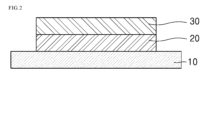
- FIG. 2 is a view illustrating a laminate in which a substrate layer, a first electrode layer, a hole transport layer, according to the present invention.
- a method for manufacturing a perovskite solar cell according to the present invention is described below with reference to FIG. 2 .
- a hole transport layer (HTL) 30 of a laminate in which a substrate layer 10, a first electrode layer 20, and the hole transport layer 30 including metal oxide are sequentially laminated is treated with a) an oxidative agent, b) ultraviolet light and ozone, c) oxygen plasma, or d) nitrogen dioxide gas to oxidize the metal oxide (step S 1).
- the hole mobility or hole extraction efficiency of the hole transport layer 30 may be improved without damaging the substrate layer 10 or the first electrode layer 20.
- any material that oxidizes metal oxide to improve metal vacancies in the hole transport layer or increases the oxidation number of metal ions can be used, but specifically, H 2 O 2 , HNO 3 , H 2 SO 4 , KNO 3 and the like may be used.
- step S1 may include treating the hole transport layer 30 with a solution containing the oxidative agent to oxidize the metal oxide, and then removing a solvent included in the solution.
- a solution process such as spin-coating the solution containing the oxidative agent on an upper surface of the hole transport layer 30, or dipping coating in which the laminate is dipped into the solution, is performed, then the metal oxide is oxidized, and then the solvent is removed by evaporation.
- the solvent may be a volatile solvent in order to facilitate subsequent evaporation, and more specifically, an alcohol including deionized water, ethyl ether, acetone, ethanol, methanol, isopropyl alcohol, and the like, but is not limited thereto.
- heat may be applied at a temperature of 150° C. or less to prevent damage to perovskite.
- the ultraviolet and ozone treatment according to the present invention may be performed for at least 5 minutes to oxide the metal oxide.
- the oxygen plasma treatment of the present invention may be a low-temperature oxygen plasma treatment maintained at a temperature of less than 200° C.
- the nitrogen dioxide gas treatment of the present invention may be performed to oxidize the metal oxide by flowing dry air containing nitrogen dioxide onto the upper surface of the hole transport layer 30.
- the concentration of nitrogen dioxide in the dry air may be 5 to 1,000 ppm, and the temperature may be maintained at 25 to 35° C.
- the step of oxidizing the metal oxide only the surface of the hole transport layer 30 may be oxidized or the entire hole transport layer 30 may be oxidized.
- the substrate layer 10 may include a transparent material that transmits light.
- the substrate layer 10 may include a material that selectively transmits light of a desired wavelength.
- the substrate layer 10 may include, for example, transparent conductive oxide (TCO) such as silicon oxide, aluminum oxide, indium tin oxide (ITO), and fluorine tin oxide (FTO), glass, quartz, or a polymer.
- TCO transparent conductive oxide
- ITO indium tin oxide
- FTO fluorine tin oxide
- the polymer may include at least one of polyimide, polyethylenenaphthalate (PEN), polyethyleneterephthalate (PET), polymethylmethacrylate (PMMA), or polydimethylsiloxane (PDMS).
- the substrate layer 10 may have a thickness ranging from, for example, 100 ⁇ m to 150 ⁇ m, and may have, for example, 125 ⁇ m.
- the material and thickness of the substrate layer 10 are not limited to the examples described above, and may be suitably selected according to the technical idea of the present invention.
- the first electrode layer 20 may be formed of a light-transmitting conductive material.
- the light-transmitting conductive material may include, for example, transparent conductive oxides, carbonaceous conductive materials, metallic materials, and the like.
- the transparent conductive oxides may include, for example, indium tin oxide (ITO), indium cerium oxide (ICO), indium tungsten oxide (IWO), zinc indium tin oxide (ZITO), zinc indium oxide (ZIO), zinc tin oxide (ZTO), gallium indium tin oxide (GITO), gallium indium oxide (GIO), gallium zinc oxide (GZO), aluminum doped zinc oxide (AZO), fluorine tin oxide (FTO), ZnO, and the like.
- ITO indium tin oxide
- ICO indium cerium oxide
- IWO indium tungsten oxide
- ZITO zinc indium tin oxide
- ZIO zinc indium oxide
- ZTO zinc tin oxide
- GITO gallium indium
- the carbonaceous conductive material for example, graphene or carbon nanotubes may be used, and as the metallic material, for example, metal (Ag) nanowires or multi-layered metal thin films such as Au/Ag/Cu/Mg/Mo/Ti may be used.
- the term "transparent” refers to the ability to transmit light to a certain extent, and is not necessarily interpreted as meaning complete transparency.
- the materials listed above are not limited to the embodiments described above and may be made of various materials, and various modifications of the structure thereof may be possible, such as a single layer structure or a multi-layered structure.
- the first electrode layer 20 may be formed by being laminated on the substrate layer 10 or may be integrally formed with the substrate layer 10.
- the hole transport layer 30 may be laminated on the first electrode layer 20, which serves to transfer holes generated in a perovskite layer 40 to the first electrode layer 20.
- the hole transport layer 30 may include at least one of metal oxides selected from tungsten oxide (WO x ), molybdenum oxide (MoO x ), vanadium oxide (V 2 O 5 ), nickel oxide (NiO x ), and mixtures thereof.
- the hole transport layer 30 may include at least one selected from the group consisting of unimolecular hole transport materials and polymer hole transport materials, but is not limited thereto, and materials used in the art may be used without limitation.
- spiro-MeOTAD [2,2',7,7'-tetrakis(N,Np-dimethoxy-phenylamino)-9,9'-spirobifluorene] may be used as the unimolecular hole transport material
- P3HT poly(3-hexylthiophene)]
- PTAA polytriarylamine
- PEDOT:PSS polystyrene sulfonate
- the hole transport layer 30 may further include a doping material, and the doping material may include a dopant selected from the group consisting of a Li-based dopant, a Co-based dopant, a Cu-based dopant, a Cs-based dopant, and combinations thereof, but is not limited thereto.
- the doping material may include a dopant selected from the group consisting of a Li-based dopant, a Co-based dopant, a Cu-based dopant, a Cs-based dopant, and combinations thereof, but is not limited thereto.
- the hole transport layer 30 may be formed by applying a precursor solution for a hole transport layer on the first electrode layer and drying the precursor solution, and before applying the precursor solution, the first electrode layer may be subjected to UV-ozone treatment to lower the work function of the first electrode layer 20, remove surface impurities, and perform hydrophilic treatment.
- the precursor solution may be applied using a method such as spin coating, but is not limited thereto.
- the thickness of the hole transport layer 30 formed may be 10 to 500 nm.
- the metal oxide of the hole transport layer 30 is preferably NiO x , which has advantageously high hole mobility in the material compared to other organic hole transporters or other metal oxides.
- FIG. 3 is a conceptual diagram illustrating Ni vacancies in the hole transport layer 30 that are improved through treatment with an oxidative agent, according to an embodiment of the present invention.
- the NiO x may be oxidized to improve Ni vacancies in the hole transport layer in step S1.
- the NiO x may be oxidized to oxidize a part of Ni 2+ included in the hole transport layer to Ni 3+ .
- the hole mobility is increased and resistance is reduced, thereby improving the hole extraction efficiency of the hole transport layer 30.
- the ratio between the content of Ni 3+ and the total content of Ni 2+ and Ni 3+ is 0.6 or less, specifically, 0.3 or less. At this time, if the ratio of the contents exceeds 0.6, that is, if the content of Ni 3+ is excessively high, optical transmittance may be reduced. In addition, as the proportion of Ni 3+ increases, a valence band maximum (VBM) of the hole transport layer 30 shifts downward.
- VBM valence band maximum
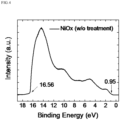
- FIG. 4 is a graph showing UPS analysis results when a hole transport layer containing NiO x is not oxidized
- FIG. 5 is a graph showing UPS analysis results when a hole transport layer containing NiO x is oxidized
- Table 1 shows work function and valence band edge values for each of the cases.
- Table 1 NiO x (w/o treatment)
- NiO x (w/ treatment) Work function 4.66 5.16 Valence band edge 5.61 5.69
- the perovskite layer 40, an electron transport layer 50, and a second electrode layer 60 are sequentially laminated on the hole transport layer 30 of the laminate (step S2).
- a perovskite compound is used as a photoactive material that absorbs sunlight to generate photoelectron-optical hole pairs.
- Perovskite advantageously has a direct band gap, an optical absorption coefficient as high as 1.5 ⁇ 10 4 cm -1 at 550 nm, excellent charge transfer characteristics, and superior resistance to defects.
- the perovskite compound has advantages in that the light absorber may be formed by a simple, easy, and low-cost process of applying and drying a solution, a light absorber composed of coarse grains may be formed due to spontaneous crystallization caused by drying of the applied solution, and conductivity for both of the electron and hole is excellent.
- This perovskite compound may be represented by the structure of Formula 1 below. [Formula 1] ABX 3
- A is a monovalent organic ammonium cation or metal cation
- B is a divalent metal cation
- X is a halogen anion
- the perovskite compound may include, for example, CH 3 NH 3 PbI 3 , CH 3 NH 3 PbI x Cl 3-x , MAPbI 3 , CH 3 NH 3 PbI x Br 3-x , CH 3 NH 3 PbCl x Br 3-x , HC(NH 2 ) 2 PbI 3 , HC(NH 2 ) 2 PbI x Cl 3-x , HC(NH 2 ) 2 PbI x Br 3-x , HC(NH 2 ) 2 PbCl x Br 3-x , (CH 3 NH 3 )(HC(NH 2 ) 2 ) 1-y PbI 3 , (CH 3 NH 3 )(HC(NH 2 ) 2 ) 1-y PbI x Cl 3-x , (CH 3 NH 3 )(HC(NH 2 ) 2 ) 1-y PbI x Cl 3-x , (CH 3 NH 3 )(HC(NH 2 ) 2 ) 1-y Pb
- the electron transport layer 50 may be located on the perovskite layer 40, may serve to facilitate transfer of electrons generated in the perovskite layer 40 to the second electrode layer 60.
- the electron transport layer 50 may include metal oxides. For example, Ti oxides, Zn oxides, In oxides, Sn oxides, W oxides, Nb oxides, Mo oxides, Mg oxides, Zr oxides, Sr oxides, Yr oxides, La oxides, V oxides, Al oxides, Y oxides, Sc oxides, Sm oxides, Ga oxides, SrTi oxides, and the like may be used.
- the electron transport layer 50 may include a compact structure of TiO 2 , SnO 2 , WO 3 , or TiSrO 3 .
- the electron transport layer 50 may further include an n-type or p-type dopant as needed.
- the perovskite layer 40, and/or the electron transport layer 50 various layer structures and materials constituting the perovskite solar cell 100 may be applied, and the hole transport layer 30 and the electron transport layer 50 may be formed by swapping their positions.
- the second electrode layer 60 may be formed of a light-transmitting conductive material.
- the light-transmitting conductive material may include, for example, transparent conductive oxides, carbonaceous conductive materials, metallic materials, and the like.
- the transparent conductive oxides may include, for example, indium tin oxide (ITO), indium cerium oxide (ICO), indium tungsten oxide (IWO), zinc indium tin oxide (ZITO), zinc indium oxide (ZIO), zinc tin oxide (ZTO), gallium indium tin oxide (GITO), gallium indium oxide (GIO), gallium zinc oxide (GZO), aluminum doped zinc oxide (AZO), fluorine tin oxide (FTO), ZnO, and the like.
- ITO indium tin oxide
- ICO indium cerium oxide
- IWO indium tungsten oxide
- ZITO zinc indium tin oxide
- ZIO zinc indium oxide
- ZTO zinc tin oxide
- GITO gallium indium
- the carbonaceous conductive material for example, graphene or carbon nanotubes may be used, and as the metallic material, for example, metal (Ag) nanowires or multi-layered metal thin films such as Au/Ag/Cu/Mg/Mo/Ti may be used.
- the term "transparent” refers to the ability to transmit light to a certain extent, and is not necessarily interpreted as meaning complete transparency.
- the materials listed above are not limited to the embodiments described above and may be made of various materials, and various modifications of the structure thereof may be possible, such as a single layer structure or a multi-layered structure.
- a bus electrode (not shown) may be further disposed on the second electrode layer 60 to lower the resistance of the second electrode layer 60 and further facilitate transfer of charges.
- the bus electrode may be made of Ag, Mg, Al, Pt, Pd, Au, Ni, Nd, Ir, Cr and/or a compound thereof.
Landscapes
- Physics & Mathematics (AREA)
- Electromagnetism (AREA)
- Engineering & Computer Science (AREA)
- Chemical & Material Sciences (AREA)
- Materials Engineering (AREA)
- Manufacturing & Machinery (AREA)
- Nanotechnology (AREA)
- Photovoltaic Devices (AREA)
Abstract
Description
- The present invention relates to a method for manufacturing a perovskite solar cell and a perovskite solar cell manufactured thereby, and more particularly, to a method for manufacturing a perovskite solar cell capable of improving hole mobility of a hole transport layer while minimizing damage to other components, and a perovskite solar cell manufactured thereby.
- Solar cells are core elements of solar-light power generation, which convert sunlight directly into electricity, and they are currently widely used for power supply purpose not only in homes but also in space. Recently, they have been used in the fields of aviation, meteorology, and communications, and the products such as solar-powered cars and solar-air conditioners are attracting attention.
- These solar cells mainly use silicon semiconductors. Due to the price of raw materials of high-purity silicon semiconductors and the complexity of a solar cell manufacture process using the same, the unit cost of power generation is disadvantageously high. That is, it is 3 to 10 times higher than the unit cost of conventional power generation with fossil fuels, and hence the market is growing with subsidies from governments around the world. For this reason, the development and research of solar cells that do not use silicon have been actively conducted, and studies on polymer solar cells using dye-sensitized solar cells (DSSC), which use a dye that is an organic semiconductor material, and conductive polymers have been promoted since the 1990s. Despite many efforts by academics and industries, organic semiconductor-based solar cells, such as DSSC and polymer solar cells, have not yet been commercialized. However, with the advent of perovskite solar cells (PSC) that incorporate the advantages of the DSSC and the polymer solar cells, expectations for next-generation solar cells are rising.
- A perovskite solar cell is a solar cell which combines a conventional DSSC and a polymer solar cell, and has improved reliability because it does not use liquid electrolyte as in DSSC. Also, the perovskite solar cell is a high efficiency solar cell due to the optical excellence of perovskite, and the efficiency is continuously improved through process improvement, material improvement, and structural improvement.
-
FIG. 1 is a view illustrating a perovskite solar cell. Referring toFIG. 1 , a perovskitesolar cell 100 includes asubstrate layer 10, afirst electrode layer 20, ahole transport layer 30, aperovskite layer 40, anelectron transport layer 50, and asecond electrode layer 60. - In the perovskite
solar cell 100, mobility of electrons or holes in each layer is important, but charge extraction at the interface between each layer is also critical. If charges are not rapidly extracted at the interface, electrons and holes may recombine. - For example, NiOx contained in the
hole transport layer 30 has high hole mobility in a material compared to organic hole transporters, but hole extraction is not effectively performed at the interface with theperovskite layer 40, which may adversely affect the characteristics of thesolar cell 100. Ni vacancies may be adjusted using an additive or high heat in order to improve the hole extraction efficiency. However, indium tin oxide (ITO), which is mainly used for thesubstrate layer 10 or thefirst electrode layer 20 laminated on a lower surface of thehole transport layer 30, is damaged by high heat treatment, such as a significant increase in resistance at a temperature of 200° C. or higher. Therefore, a method for improving the hole extraction efficiency without damaging thesubstrate layer 10 or thefirst electrode layer 20 is needed. - Therefore, the present invention aims to provide a method for manufacturing a perovskite solar cell capable of improving the hole mobility and hole extraction efficiency of a hole transport layer while minimizing damage to a substrate layer or an electrode layer, and a perovskite solar cell produced thereby.
- To achieve the above object, a method for manufacturing a perovskite solar cell according to one aspect of the present invention includes the steps of: (S1) applying a) an oxidative agent, b) ultraviolet light and ozone, c) oxygen plasma, or d) nitrogen dioxide gas to a hole transport layer (HTL) of a laminate in which a substrate layer, a first electrode layer, and the hole transport layer (HTL) containing a metal oxide are sequentially laminated, to oxidize the metal oxide; and (S2) sequentially laminating a perovskite layer, an electron transport layer, and a second electrode layer on the hole transport layer of the laminate.
- Here, the step S1 may further include treating the hole transport layer with a solution containing the oxidative agent to oxidize the metal oxide, and then removing a solvent included in the solution.
- The metal oxide in the step S1 may be NiOx.
- At this time, in the step S1, the NiOx may be oxidized to improve Ni vacancies in the hole transport layer.
- In the step S1, the NiOx may be oxidized to oxidize a part of Ni2+ included in the hole transport layer to Ni3+.
- In this case, a ratio between the content of Ni3+ and the total content of Ni2+ and Ni3+ may be 0.6 or less.
- Meanwhile, the first electrode layer and the second electrode layer may include, independently of each other, at least one selected from the group consisting of indium tin oxide (ITO), indium cerium oxide (ICO), indium tungsten oxide (IWO), zinc indium tin oxide (ZITO), zinc indium oxide (ZIO), zinc tin oxide (ZTO), gallium indium tin oxide (GITO), gallium indium oxide (GIO), gallium zinc oxide (GZO), aluminum doped zinc oxide (AZO), fluorine tin oxide (FTO), and ZnO.
- In addition, the electron transport layer may include at least one selected from the group consisting of Ti oxide, Zn oxide, In oxide, Sn oxide, W oxide, Nb oxide, Mo oxide, Mg oxide, Zr oxide, Sr oxide, Yr oxide, La oxide, V oxide, Al oxide, Y oxide, Sc oxide, Sm oxide, Ga oxide, and SrTi oxide.
- A perovskite solar cell according to another aspect of the present invention is formed by sequentially laminating a substrate layer, a first electrode layer, a hole transport layer (HTL) including a metal oxide, a perovskite layer, an electron transport layer, and a second electrode layer, wherein the metal oxide is NiOx and the hole transport layer includes Ni2+ and Ni3+.
- According to the present invention, a metal oxide included in a hole transport layer is oxidized by applying a) an oxidative agent, b) ultraviolet light and ozone, c) oxygen plasma, or d) nitrogen dioxide gas to the hole transport layer without heat treatment at a high temperature of 200° C. or higher, so that the hole mobility or hole extraction efficiency of the hole transport layer may be improved without damaging the substrate layer or the first electrode layer.
- As such, when the hole extraction efficiency of the hole transport layer is improved, recombination due to inefficient hole extraction at the interface with the perovskite layer is prevented, ultimately improving the photoelectric conversion efficiency.
- The accompanying drawings illustrate preferred embodiments of the present invention and, together with the foregoing disclosure, serve to provide further understanding of the technical features of the present invention. However, the present invention is not to be construed as being limited to the drawings.
-
FIG. 1 is a side view illustrating a perovskite solar cell. -
FIG. 2 is a side view illustrating a laminate in which a substrate layer, a first electrode layer, and a hole transport layer are laminated, according to the present invention. -
FIG. 3 is a conceptual diagram illustrating Ni vacancies in a hole transport layer that are improved through treatment with an oxidative agent, according to an embodiment of the present invention. -
FIG. 4 is a graph showing UPS analysis results when a hole transport layer containing NiOx is not oxidized. -
FIG. 5 is a graph showing UPS analysis results when a hole transport layer containing NiOx is oxidized. - Hereinafter, the present invention will be described with reference to the accompanying drawings. Prior to the description, it should be understood that the terms used in the specification and the appended claims should not be construed as limited to general and dictionary meanings, but interpreted based on the meanings and concepts corresponding to technical aspects of the present invention on the basis of the principle that the inventor is allowed to define terms appropriately for the best explanation.
- Therefore, the description proposed herein is just a preferable example for the purpose of illustrations only, and not intended to limit the scope of the invention, so it should be understood that other equivalents and modifications could be made thereto without departing from the spirit and scope of the invention.
-
FIG. 2 is a view illustrating a laminate in which a substrate layer, a first electrode layer, a hole transport layer, according to the present invention. A method for manufacturing a perovskite solar cell according to the present invention is described below with reference toFIG. 2 . - First, a hole transport layer (HTL) 30 of a laminate in which a
substrate layer 10, afirst electrode layer 20, and thehole transport layer 30 including metal oxide are sequentially laminated is treated with a) an oxidative agent, b) ultraviolet light and ozone, c) oxygen plasma, or d) nitrogen dioxide gas to oxidize the metal oxide (step S 1). - As such, by oxidizing the metal oxide included in the
hole transport layer 30 through the above methods, such as treating thehole transport layer 30 with an oxidative agent, without applying heat treatment at a high temperature of 200° C. or higher, the hole mobility or hole extraction efficiency of thehole transport layer 30 may be improved without damaging thesubstrate layer 10 or thefirst electrode layer 20. - At this time, as the oxidative agent, any material that oxidizes metal oxide to improve metal vacancies in the hole transport layer or increases the oxidation number of metal ions can be used, but specifically, H2O2, HNO3, H2SO4, KNO3 and the like may be used.
- Here, step S1 may include treating the
hole transport layer 30 with a solution containing the oxidative agent to oxidize the metal oxide, and then removing a solvent included in the solution. - At this time, a solution process, such as spin-coating the solution containing the oxidative agent on an upper surface of the
hole transport layer 30, or dipping coating in which the laminate is dipped into the solution, is performed, then the metal oxide is oxidized, and then the solvent is removed by evaporation. - The solvent may be a volatile solvent in order to facilitate subsequent evaporation, and more specifically, an alcohol including deionized water, ethyl ether, acetone, ethanol, methanol, isopropyl alcohol, and the like, but is not limited thereto. During evaporation of the solvent, heat may be applied at a temperature of 150° C. or less to prevent damage to perovskite.
- In addition, the ultraviolet and ozone treatment according to the present invention may be performed for at least 5 minutes to oxide the metal oxide.
- Also, the oxygen plasma treatment of the present invention may be a low-temperature oxygen plasma treatment maintained at a temperature of less than 200° C.
- Moreover, the nitrogen dioxide gas treatment of the present invention may be performed to oxidize the metal oxide by flowing dry air containing nitrogen dioxide onto the upper surface of the
hole transport layer 30. At this time, the concentration of nitrogen dioxide in the dry air may be 5 to 1,000 ppm, and the temperature may be maintained at 25 to 35° C. - Through the step of oxidizing the metal oxide, only the surface of the
hole transport layer 30 may be oxidized or the entirehole transport layer 30 may be oxidized. - The
substrate layer 10 may include a transparent material that transmits light. In addition, thesubstrate layer 10 may include a material that selectively transmits light of a desired wavelength. Thesubstrate layer 10 may include, for example, transparent conductive oxide (TCO) such as silicon oxide, aluminum oxide, indium tin oxide (ITO), and fluorine tin oxide (FTO), glass, quartz, or a polymer. For example, the polymer may include at least one of polyimide, polyethylenenaphthalate (PEN), polyethyleneterephthalate (PET), polymethylmethacrylate (PMMA), or polydimethylsiloxane (PDMS). - The
substrate layer 10 may have a thickness ranging from, for example, 100 µm to 150 µm, and may have, for example, 125 µm. However, the material and thickness of thesubstrate layer 10 are not limited to the examples described above, and may be suitably selected according to the technical idea of the present invention. - The
first electrode layer 20 may be formed of a light-transmitting conductive material. The light-transmitting conductive material may include, for example, transparent conductive oxides, carbonaceous conductive materials, metallic materials, and the like. The transparent conductive oxides may include, for example, indium tin oxide (ITO), indium cerium oxide (ICO), indium tungsten oxide (IWO), zinc indium tin oxide (ZITO), zinc indium oxide (ZIO), zinc tin oxide (ZTO), gallium indium tin oxide (GITO), gallium indium oxide (GIO), gallium zinc oxide (GZO), aluminum doped zinc oxide (AZO), fluorine tin oxide (FTO), ZnO, and the like. As the carbonaceous conductive material, for example, graphene or carbon nanotubes may be used, and as the metallic material, for example, metal (Ag) nanowires or multi-layered metal thin films such as Au/Ag/Cu/Mg/Mo/Ti may be used. As used herein, the term "transparent" refers to the ability to transmit light to a certain extent, and is not necessarily interpreted as meaning complete transparency. The materials listed above are not limited to the embodiments described above and may be made of various materials, and various modifications of the structure thereof may be possible, such as a single layer structure or a multi-layered structure. - At this time, the
first electrode layer 20 may be formed by being laminated on thesubstrate layer 10 or may be integrally formed with thesubstrate layer 10. - Also, the
hole transport layer 30 may be laminated on thefirst electrode layer 20, which serves to transfer holes generated in aperovskite layer 40 to thefirst electrode layer 20. Thehole transport layer 30 may include at least one of metal oxides selected from tungsten oxide (WOx), molybdenum oxide (MoOx), vanadium oxide (V2O5), nickel oxide (NiOx), and mixtures thereof. In addition, thehole transport layer 30 may include at least one selected from the group consisting of unimolecular hole transport materials and polymer hole transport materials, but is not limited thereto, and materials used in the art may be used without limitation. For example, spiro-MeOTAD [2,2',7,7'-tetrakis(N,Np-dimethoxy-phenylamino)-9,9'-spirobifluorene] may be used as the unimolecular hole transport material, and P3HT [poly(3-hexylthiophene)], PTAA (polytriarylamine), poly(3,4-ethylenedioxythiophene), or polystyrene sulfonate (PEDOT:PSS) may be used as the polymer hole transport material, but the present invention is not limited thereto. - In addition, the
hole transport layer 30 may further include a doping material, and the doping material may include a dopant selected from the group consisting of a Li-based dopant, a Co-based dopant, a Cu-based dopant, a Cs-based dopant, and combinations thereof, but is not limited thereto. - The
hole transport layer 30 may be formed by applying a precursor solution for a hole transport layer on the first electrode layer and drying the precursor solution, and before applying the precursor solution, the first electrode layer may be subjected to UV-ozone treatment to lower the work function of thefirst electrode layer 20, remove surface impurities, and perform hydrophilic treatment. The precursor solution may be applied using a method such as spin coating, but is not limited thereto. The thickness of thehole transport layer 30 formed may be 10 to 500 nm. - At this time, the metal oxide of the
hole transport layer 30 is preferably NiOx, which has advantageously high hole mobility in the material compared to other organic hole transporters or other metal oxides. -
FIG. 3 is a conceptual diagram illustrating Ni vacancies in thehole transport layer 30 that are improved through treatment with an oxidative agent, according to an embodiment of the present invention. Referring toFIG. 3 , the NiOx may be oxidized to improve Ni vacancies in the hole transport layer in step S1. In addition, the NiOx may be oxidized to oxidize a part of Ni2+ included in the hole transport layer to Ni3+. As such, when the Ni vacancies are increased or a part of Ni2+ is oxidized to Ni3+, the hole mobility is increased and resistance is reduced, thereby improving the hole extraction efficiency of thehole transport layer 30. - Here, the ratio between the content of Ni3+ and the total content of Ni2+ and Ni3+ is 0.6 or less, specifically, 0.3 or less. At this time, if the ratio of the contents exceeds 0.6, that is, if the content of Ni3+ is excessively high, optical transmittance may be reduced. In addition, as the proportion of Ni3+ increases, a valence band maximum (VBM) of the
hole transport layer 30 shifts downward. When the ratio of the content of Ni3+ and the total content of Ni2+ and Ni3+ is approximately 0.6, more preferably, approximately 0.3, energy matching with the perovskite layer occurs well, resulting in effective charge extraction. If the content of Ni3+ is excessively high and thus the VBM (work function) excessively drops, mismatch in energy level alignment occurs at the interference with the perovskite, leading to a problem of interfering hole extraction at the interface. -
FIG. 4 is a graph showing UPS analysis results when a hole transport layer containing NiOx is not oxidized,FIG. 5 is a graph showing UPS analysis results when a hole transport layer containing NiOx is oxidized, and Table 1 below shows work function and valence band edge values for each of the cases.Table 1 NiOx (w/o treatment) NiOx (w/ treatment) Work function 4.66 5.16 Valence band edge 5.61 5.69 - It can be seen that, as the proportion of Ni3+ increases after oxidization of NiOx, the value of the work function increases and approaches the value of the Valence band edge, which means that there is an effect similar to p-type doping. 1) in the case of NiOx (w/o treatment)
- Work function: 21.22eV(He|UPS spectra)-16.56eV = 4.66 eV
- Valence band edge: 4.66 (Work function) eV + 0.95 eV = 5.61 eV
- Work function: 21.22eV(He|UPS spectra) - 16.56eV = 5.16 eV
- Valence band edge: 5.16 (Work function) eV + 0.53 eV = 5.69 eV
- Subsequently, the
perovskite layer 40, anelectron transport layer 50, and asecond electrode layer 60 are sequentially laminated on thehole transport layer 30 of the laminate (step S2). - In the perovskite
solar cell 100 according to the present invention, a perovskite compound is used as a photoactive material that absorbs sunlight to generate photoelectron-optical hole pairs. Perovskite advantageously has a direct band gap, an optical absorption coefficient as high as 1.5×104 cm-1 at 550 nm, excellent charge transfer characteristics, and superior resistance to defects. - In addition, the perovskite compound has advantages in that the light absorber may be formed by a simple, easy, and low-cost process of applying and drying a solution, a light absorber composed of coarse grains may be formed due to spontaneous crystallization caused by drying of the applied solution, and conductivity for both of the electron and hole is excellent.
- This perovskite compound may be represented by the structure of Formula 1 below.
[Formula 1] ABX3
- The perovskite compound may include, for example, CH3NH3PbI3, CH3NH3PbIxCl3-x, MAPbI3, CH3NH3PbIxBr3-x, CH3NH3PbClxBr3-x, HC(NH2)2PbI3, HC(NH2)2PbIxCl3-x, HC(NH2)2PbIxBr3-x, HC(NH2)2PbClxBr3-x, (CH3NH3)(HC(NH2)2)1-yPbI3, (CH3NH3)(HC(NH2)2)1-yPbIxCl3-x, (CH3NH3)(HC(NH2)2)1-yPbIxBr3-x, (CH3NH3)(HC(NH2)2)1-yPbClxBr3-x, and the like (0≤x, y≤1). In addition, a compound in which A of ABX3 is partially doped with Cs may also be used.
- The
electron transport layer 50 may be located on theperovskite layer 40, may serve to facilitate transfer of electrons generated in theperovskite layer 40 to thesecond electrode layer 60. Theelectron transport layer 50 may include metal oxides. For example, Ti oxides, Zn oxides, In oxides, Sn oxides, W oxides, Nb oxides, Mo oxides, Mg oxides, Zr oxides, Sr oxides, Yr oxides, La oxides, V oxides, Al oxides, Y oxides, Sc oxides, Sm oxides, Ga oxides, SrTi oxides, and the like may be used. Theelectron transport layer 50 according to the present invention may include a compact structure of TiO2, SnO2, WO3, or TiSrO3. Theelectron transport layer 50 may further include an n-type or p-type dopant as needed. - In addition to the above-described interlayer structures and/or materials of the
hole transport layer 30, theperovskite layer 40, and/or theelectron transport layer 50, various layer structures and materials constituting the perovskitesolar cell 100 may be applied, and thehole transport layer 30 and theelectron transport layer 50 may be formed by swapping their positions. - In addition, the
second electrode layer 60 may be formed of a light-transmitting conductive material. The light-transmitting conductive material may include, for example, transparent conductive oxides, carbonaceous conductive materials, metallic materials, and the like. The transparent conductive oxides may include, for example, indium tin oxide (ITO), indium cerium oxide (ICO), indium tungsten oxide (IWO), zinc indium tin oxide (ZITO), zinc indium oxide (ZIO), zinc tin oxide (ZTO), gallium indium tin oxide (GITO), gallium indium oxide (GIO), gallium zinc oxide (GZO), aluminum doped zinc oxide (AZO), fluorine tin oxide (FTO), ZnO, and the like. As the carbonaceous conductive material, for example, graphene or carbon nanotubes may be used, and as the metallic material, for example, metal (Ag) nanowires or multi-layered metal thin films such as Au/Ag/Cu/Mg/Mo/Ti may be used. As used herein, the term "transparent" refers to the ability to transmit light to a certain extent, and is not necessarily interpreted as meaning complete transparency. The materials listed above are not limited to the embodiments described above and may be made of various materials, and various modifications of the structure thereof may be possible, such as a single layer structure or a multi-layered structure. - Although not illustrated, a bus electrode (not shown) may be further disposed on the
second electrode layer 60 to lower the resistance of thesecond electrode layer 60 and further facilitate transfer of charges. The bus electrode may be made of Ag, Mg, Al, Pt, Pd, Au, Ni, Nd, Ir, Cr and/or a compound thereof. - Meanwhile, the embodiments of the disclosure disclosed in the specification and drawings have suggested given examples in order to easily describe the technical contents of the invention and to help understanding of the disclosure, and are not intended to limit the scope of the disclosure. That is, it is evident to those skilled in the art to which the disclosure pertains that other modified examples based on technical spirit of the invention may be practiced.
Claims (10)
- A method for manufacturing a perovskite solar cell comprising the steps of:(S1) applying a) an oxidative agent, b) ultraviolet light and ozone, c) oxygen plasma, or d) nitrogen dioxide gas to a hole transport layer (HTL) of a laminate in which a substrate layer, a first electrode layer, and the hole transport layer (HTL) containing a metal oxide are sequentially laminated, to oxidize the metal oxide; and(S2) sequentially laminating a perovskite layer, an electron transport layer, and a second electrode layer on the hole transport layer of the laminate.
- The method of claim 1, wherein the step S1 further comprises treating the hole transport layer with a solution containing the oxidative agent to oxidize the metal oxide, and then removing a solvent included in the solution.
- The method of claim 1, wherein the metal oxide in the step S1 may be NiOx.
- The method of claim 3, wherein, in the step S1, the NiOx is oxidized to improve Ni vacancies in the hole transport layer.
- The method of claim 3, wherein, in the step S1, the NiOx is oxidized to oxidize a part of Ni2+ included in the hole transport layer to Ni3+.
- The method of claim 5, wherein a ratio between the content of Ni3+ and the total content of Ni2+ and Ni3+ is 0.6 or less.
- The method of claim 1, wherein the first electrode layer and the second electrode layer comprise, independently of each other, at least one selected from the group consisting of indium tin oxide (ITO), indium cerium oxide (ICO), indium tungsten oxide (IWO), zinc indium tin oxide (ZITO), zinc indium oxide (ZIO), zinc tin oxide (ZTO), gallium indium tin oxide (GITO), gallium indium oxide (GIO), gallium zinc oxide (GZO), aluminum doped zinc oxide (AZO), fluorine tin oxide (FTO), and ZnO.
- The method of claim 1, wherein the electron transport layer comprises at least one selected from the group consisting of Ti oxide, Zn oxide, In oxide, Sn oxide, W oxide, Nb oxide, Mo oxide, Mg oxide, Zr oxide, Sr oxide, Yr oxide, La oxide, V oxide, Al oxide, Y oxide, Sc oxide, Sm oxide, Ga oxide, and SrTi oxide.
- A perovskite solar cell being formed by sequentially laminating a substrate layer, a first electrode layer, a hole transport layer (HTL) including a metal oxide, a perovskite layer, an electron transport layer, and a second electrode layer, wherein the metal oxide is NiOx and the hole transport layer includes Ni2+ and Ni3+.
- The perovskite solar cell of claim 9, wherein a ratio between the content of Ni3+ and the total content of Ni2+ and Ni3+ is 0.6 or less.
Applications Claiming Priority (2)
| Application Number | Priority Date | Filing Date | Title |
|---|---|---|---|
| KR1020200084012A KR102401218B1 (en) | 2020-07-08 | 2020-07-08 | Matufacturing method for perovskite solar cell and perovskite solar cell manufactured by the same method |
| PCT/KR2021/008061 WO2022010147A1 (en) | 2020-07-08 | 2021-06-28 | Method for manufacturing perovskite solar cell and perovskite solar cell manufactured thereby |
Publications (2)
| Publication Number | Publication Date |
|---|---|
| EP4160709A1 true EP4160709A1 (en) | 2023-04-05 |
| EP4160709A4 EP4160709A4 (en) | 2023-12-06 |
Family
ID=79552523
Family Applications (1)
| Application Number | Title | Priority Date | Filing Date |
|---|---|---|---|
| EP21838202.6A Pending EP4160709A4 (en) | 2020-07-08 | 2021-06-28 | METHOD FOR PRODUCING A PEROWSKITE SOLAR CELL AND PEROWSKITE SOLAR CELL PRODUCED THEREFROM |
Country Status (6)
| Country | Link |
|---|---|
| US (2) | US12604596B2 (en) |
| EP (1) | EP4160709A4 (en) |
| JP (1) | JP7654697B2 (en) |
| KR (1) | KR102401218B1 (en) |
| CN (1) | CN115777240A (en) |
| WO (1) | WO2022010147A1 (en) |
Families Citing this family (15)
| Publication number | Priority date | Publication date | Assignee | Title |
|---|---|---|---|---|
| CN117178650A (en) * | 2022-03-09 | 2023-12-05 | 宁德时代新能源科技股份有限公司 | Perovskite solar cells and preparation methods thereof |
| KR20230167963A (en) | 2022-06-03 | 2023-12-12 | 한국전력공사 | Perovskite solar cell and method for manufacturing the same |
| KR102736201B1 (en) | 2022-06-23 | 2024-12-02 | 고려대학교 산학협력단 | A perovskite photoelectric device and manufacturing method thereof |
| CN115083787B (en) * | 2022-06-23 | 2024-09-10 | 南京邮电大学 | Ultrathin oxide modified semiconductor electrode and preparation method thereof |
| CN117580415A (en) * | 2022-08-04 | 2024-02-20 | 杭州纤纳光电科技有限公司 | A kind of preparation method of perovskite solar cell |
| CN115425154B (en) * | 2022-09-06 | 2025-05-02 | 旗滨新能源发展(深圳)有限责任公司 | A method for preparing a perovskite solar cell module |
| CN116081711B (en) * | 2022-12-08 | 2024-10-29 | 武汉大学 | Oleate modified nickel oxide nanocrystalline material and preparation method and application thereof |
| CN116075164B (en) * | 2023-03-06 | 2023-07-28 | 宁德时代新能源科技股份有限公司 | Perovskite battery, preparation method and corresponding electrical device |
| KR102766237B1 (en) | 2023-03-06 | 2025-02-12 | 고려대학교 산학협력단 | Method for manufacturing an electron transport layer solution, method for manufacturing an electron transport layer using the same, electron transport layer manufactured through the same, method for manufacturing a perovskite solar cell including the same, and a perovskite solar cell manufactured through the same |
| TWI844323B (en) * | 2023-03-29 | 2024-06-01 | 國立陽明交通大學 | Perovskite optoelectronic device and self-adaptive transport layer structure applied to perovskite optoelectronic device |
| EP4723847A1 (en) * | 2023-05-26 | 2026-04-08 | Jusung Engineering Co., Ltd. | Solar cell and method for forming same |
| KR20250018139A (en) | 2023-07-28 | 2025-02-04 | 고려대학교 산학협력단 | Self-classifying smart devices and its manufacturing method |
| KR102853063B1 (en) | 2024-03-07 | 2025-09-03 | 고려대학교 산학협력단 | A perovskite photoelectric device and manufacturing method thereof |
| WO2025199279A1 (en) * | 2024-03-20 | 2025-09-25 | Northwestern University | Perovskite solar cells with dual site binding ligands |
| JP2026006155A (en) | 2024-06-28 | 2026-01-16 | トヨタ自動車株式会社 | Method for manufacturing a solar cell module, and a solar cell module |
Family Cites Families (30)
| Publication number | Priority date | Publication date | Assignee | Title |
|---|---|---|---|---|
| US5413667A (en) * | 1992-11-04 | 1995-05-09 | Matsushita Electric Industrial Co., Ltd. | Pyroelectric infrared detector fabricating method |
| JP2008016868A (en) * | 2003-12-16 | 2008-01-24 | Matsushita Electric Ind Co Ltd | Organic electroluminescent device and manufacturing method thereof |
| KR100817853B1 (en) * | 2006-09-25 | 2008-03-31 | 재단법인서울대학교산학협력재단 | Quantum dots with gradual concentration gradient shell structure and preparation method thereof |
| US8860009B2 (en) | 2008-04-28 | 2014-10-14 | Dai Nippon Printing Co., Ltd. | Device comprising positive hole injection transport layer, method for producing the same and ink for forming positive hole injection transport layer |
| US12384699B2 (en) * | 2010-05-21 | 2025-08-12 | Crosstek Holding Company Llc | Self-assembled surfactant structures |
| WO2013161166A1 (en) * | 2012-04-27 | 2013-10-31 | パナソニック株式会社 | Organic el element, organic el panel provided therewith, organic el light-emitting device, and organic el display |
| TWI661072B (en) * | 2014-02-04 | 2019-06-01 | 荷蘭商Asm Ip控股公司 | Selective deposition of metals, metal oxides, and dielectrics |
| WO2015187225A2 (en) * | 2014-03-12 | 2015-12-10 | The University Of Akron | Ultrasensitive solution-processed perovskite hybrid photodetectors |
| TWI532198B (en) | 2014-07-02 | 2016-05-01 | 國立成功大學 | Solar cell and method of manufacturing same |
| JP6503080B2 (en) | 2015-02-12 | 2019-04-17 | アファンタマ アクチェンゲゼルシャフト | Optoelectronic device comprising a solution processable metal oxide buffer layer |
| DE112015006988T8 (en) * | 2015-10-02 | 2018-07-05 | The Governing Council Of The University Of Toronto | Quantum dot based optoelectronic device |
| KR20170040708A (en) * | 2015-10-05 | 2017-04-13 | 한국에너지기술연구원 | High stability of organic-inorganic hybrid photovoltaic cell Using double layer transparent electrode and method for manufacturing the same |
| US10340458B2 (en) * | 2015-10-30 | 2019-07-02 | The University Of Akron | Perovskite hybrid solar cells |
| WO2017106811A1 (en) * | 2015-12-17 | 2017-06-22 | University Of Florida Research Foundation, Inc. | Polymer passivated metal oxide surfaces and organic electronic devices therefrom |
| US20170200955A1 (en) * | 2016-01-08 | 2017-07-13 | Ford Global Technologies, Llc | Carbon Nanofiber Catalyst Substrate |
| US11355583B2 (en) * | 2016-07-28 | 2022-06-07 | Samsung Electronics Co., Ltd. | Quantum dots and devices including the same |
| KR20180033074A (en) | 2016-09-23 | 2018-04-02 | 주식회사 엘지화학 | Organic-inorganic complex solar cell and method for manufacturing same |
| US10644364B2 (en) * | 2016-10-17 | 2020-05-05 | David Fortenbacher | Self-heating cells and self-heating batteries including the self-heating cells |
| KR102345781B1 (en) * | 2017-04-28 | 2021-12-30 | 재단법인 멀티스케일 에너지시스템 연구단 | Fabrication method of a large area perovskite solar cell |
| US10388898B2 (en) * | 2017-06-05 | 2019-08-20 | Board Of Trustees Of Northern Illinois University | Doped perovskite having improved stability, and solar cells made thereof |
| US10768485B2 (en) * | 2017-07-05 | 2020-09-08 | Nanoco Technologies Ltd. | Quantum dot architectures for color filter applications |
| JP2019114691A (en) | 2017-12-25 | 2019-07-11 | 株式会社カネカ | Photovoltaic power generation device and method of manufacturing photovoltaic power generation device |
| WO2020072314A2 (en) * | 2018-09-27 | 2020-04-09 | Alliance For Sustainable Energy, Llc | Optoelectronic devices and methods of making the same |
| CN109841740A (en) | 2019-03-22 | 2019-06-04 | 上海交通大学 | A kind of preparation method of the perovskite solar cell based on nickel oxide hole transmission layer |
| WO2020213095A1 (en) * | 2019-04-17 | 2020-10-22 | シャープ株式会社 | Electroluminescent element, display device, and method for manufacturing electroluminescent element |
| US20220199925A1 (en) * | 2019-04-17 | 2022-06-23 | Sharp Kabushiki Kaisha | Electroluminescent element, display device, and method for manufacturing electroluminescent element |
| CN110310888B (en) | 2019-06-17 | 2021-03-30 | 佛山科学技术学院 | P-type nano transition metal oxide film and preparation method and application thereof |
| KR102718897B1 (en) * | 2019-10-31 | 2024-10-16 | 삼성전자주식회사 | Light emitting device, production method thereof, and display device including the same |
| KR102684641B1 (en) * | 2020-04-20 | 2024-07-12 | 삼성디스플레이 주식회사 | Cadmium free quantum dot, quantum dot-polymer composite, and electronic device including the same |
| KR102859273B1 (en) * | 2020-12-28 | 2025-09-12 | 삼성전자주식회사 | Core shell quantum dot and electronic device including the same |
-
2020
- 2020-07-08 KR KR1020200084012A patent/KR102401218B1/en active Active
-
2021
- 2021-06-28 WO PCT/KR2021/008061 patent/WO2022010147A1/en not_active Ceased
- 2021-06-28 EP EP21838202.6A patent/EP4160709A4/en active Pending
- 2021-06-28 US US18/011,611 patent/US12604596B2/en active Active
- 2021-06-28 CN CN202180046920.5A patent/CN115777240A/en active Pending
- 2021-06-28 JP JP2022579919A patent/JP7654697B2/en active Active
-
2025
- 2025-10-07 US US19/351,765 patent/US20260040751A1/en active Pending
Also Published As
| Publication number | Publication date |
|---|---|
| KR20220006264A (en) | 2022-01-17 |
| US20230363183A1 (en) | 2023-11-09 |
| WO2022010147A1 (en) | 2022-01-13 |
| KR102401218B9 (en) | 2023-02-23 |
| CN115777240A (en) | 2023-03-10 |
| KR102401218B1 (en) | 2022-05-23 |
| US20260040751A1 (en) | 2026-02-05 |
| JP2023538996A (en) | 2023-09-13 |
| JP7654697B2 (en) | 2025-04-01 |
| US12604596B2 (en) | 2026-04-14 |
| EP4160709A4 (en) | 2023-12-06 |
Similar Documents
| Publication | Publication Date | Title |
|---|---|---|
| US12604596B2 (en) | Method for manufacturing a perovskite solar cell with an improved hole transport layer and a perovskite solar cell with an improved hole transport layer manufactured by the same method | |
| Aftab et al. | Quantum junction solar cells: Development and prospects | |
| AU2019257470A1 (en) | A Photovoltaic Device | |
| KR101117127B1 (en) | Tandem solar cell using amorphous silicon solar cell and organic solar cell | |
| Fan et al. | Delayed annealing treatment for high-quality CuSCN: Exploring its impact on bifacial semitransparent nip planar perovskite solar cells | |
| CN114914365B (en) | A perovskite/perovskite tandem solar cell with an inverted structure | |
| JP7700243B2 (en) | Method for manufacturing solar cell and solar cell manufactured therefrom | |
| Tao et al. | Polyoxometalate doped tin oxide as electron transport layer for low cost, hole-transport-material-free perovskite solar cells | |
| CN109065730A (en) | A kind of method in the trans- perovskite solar battery of small organic molecule | |
| KR20220092150A (en) | Manufacturing method for perovskite solar cell and perovskite solar cell manufactured by the same method | |
| KR20260039751A (en) | Solar cell and method of manufacturing the same, photovoltaic assembly, system and electric device | |
| US20260076017A1 (en) | Composite electrode, solar cell, methods for preparing same, power consuming apparatus, and energy storage apparatus | |
| CN117337060B (en) | Laminated battery and preparation method thereof | |
| CN119947548A (en) | A perovskite/tunneling oxide layer passivated contact stacked solar cell and a method for preparing the same | |
| CN119866129A (en) | Perovskite solar cell and preparation method thereof | |
| Horta et al. | Development of metal oxide heterostructures for photovoltaic and solar cell applications | |
| KR102901157B1 (en) | Solar cell containing ammonium salt-treated metal oxide and manufacturing method thereof | |
| CN120614935A (en) | Solar cell and its preparation method, power-consuming device and power-generating device | |
| CN120917911A (en) | Perovskite solar cell, preparation method thereof and power utilization device | |
| CN114361340A (en) | Hybrid perovskite solar cell based on nano diamond and preparation method thereof | |
| KR102807900B1 (en) | A organic photoelectric and manufacturing method thereof | |
| KR102912264B1 (en) | Photoelectric device with high power in low light and method of manufacturing the same | |
| CN111211231A (en) | Solar cell based on semitransparent quantum dots and preparation method thereof | |
| Shu | Evaluation of stability and performance of an air-processed all-inorganic perovskite solar cell | |
| Tran | HIGHLY STABLE AND EFFICIENT LEAD-BASED PEROVSKITE SOLAR CELL WITH TIN-OXIDE ELECTRON TRANSPORT LAYER |
Legal Events
| Date | Code | Title | Description |
|---|---|---|---|
| STAA | Information on the status of an ep patent application or granted ep patent |
Free format text: STATUS: THE INTERNATIONAL PUBLICATION HAS BEEN MADE |
|
| PUAI | Public reference made under article 153(3) epc to a published international application that has entered the european phase |
Free format text: ORIGINAL CODE: 0009012 |
|
| STAA | Information on the status of an ep patent application or granted ep patent |
Free format text: STATUS: REQUEST FOR EXAMINATION WAS MADE |
|
| 17P | Request for examination filed |
Effective date: 20221228 |
|
| AK | Designated contracting states |
Kind code of ref document: A1 Designated state(s): AL AT BE BG CH CY CZ DE DK EE ES FI FR GB GR HR HU IE IS IT LI LT LU LV MC MK MT NL NO PL PT RO RS SE SI SK SM TR |
|
| DAV | Request for validation of the european patent (deleted) | ||
| DAX | Request for extension of the european patent (deleted) | ||
| REG | Reference to a national code |
Ref country code: DE Ref legal event code: R079 Free format text: PREVIOUS MAIN CLASS: H01L0051420000 Ipc: H10K0030400000 |
|
| A4 | Supplementary search report drawn up and despatched |
Effective date: 20231106 |
|
| RIC1 | Information provided on ipc code assigned before grant |
Ipc: H10K 85/50 20230101ALN20231030BHEP Ipc: H10K 71/30 20230101ALI20231030BHEP Ipc: H10K 30/86 20230101ALI20231030BHEP Ipc: H10K 30/50 20230101ALI20231030BHEP Ipc: H10K 30/40 20230101AFI20231030BHEP |