EP4160355A1 - Computing system and method for adjusting voltage regulation - Google Patents
Computing system and method for adjusting voltage regulation Download PDFInfo
- Publication number
- EP4160355A1 EP4160355A1 EP21306355.5A EP21306355A EP4160355A1 EP 4160355 A1 EP4160355 A1 EP 4160355A1 EP 21306355 A EP21306355 A EP 21306355A EP 4160355 A1 EP4160355 A1 EP 4160355A1
- Authority
- EP
- European Patent Office
- Prior art keywords
- processing module
- regulation
- voltage
- module
- main processing
- Prior art date
- Legal status (The legal status is an assumption and is not a legal conclusion. Google has not performed a legal analysis and makes no representation as to the accuracy of the status listed.)
- Pending
Links
Images
Classifications
-
- G—PHYSICS
- G06—COMPUTING OR CALCULATING; COUNTING
- G06F—ELECTRIC DIGITAL DATA PROCESSING
- G06F1/00—Details not covered by groups G06F3/00 - G06F13/00 and G06F21/00
- G06F1/26—Power supply means, e.g. regulation thereof
-
- G—PHYSICS
- G06—COMPUTING OR CALCULATING; COUNTING
- G06F—ELECTRIC DIGITAL DATA PROCESSING
- G06F1/00—Details not covered by groups G06F3/00 - G06F13/00 and G06F21/00
- G06F1/26—Power supply means, e.g. regulation thereof
- G06F1/32—Means for saving power
- G06F1/3203—Power management, i.e. event-based initiation of a power-saving mode
- G06F1/3234—Power saving characterised by the action undertaken
- G06F1/3296—Power saving characterised by the action undertaken by lowering the supply or operating voltage
-
- G—PHYSICS
- G06—COMPUTING OR CALCULATING; COUNTING
- G06F—ELECTRIC DIGITAL DATA PROCESSING
- G06F1/00—Details not covered by groups G06F3/00 - G06F13/00 and G06F21/00
- G06F1/26—Power supply means, e.g. regulation thereof
- G06F1/32—Means for saving power
- G06F1/3203—Power management, i.e. event-based initiation of a power-saving mode
- G06F1/3206—Monitoring of events, devices or parameters that trigger a change in power modality
- G06F1/3228—Monitoring task completion, e.g. by use of idle timers, stop commands or wait commands
-
- Y—GENERAL TAGGING OF NEW TECHNOLOGICAL DEVELOPMENTS; GENERAL TAGGING OF CROSS-SECTIONAL TECHNOLOGIES SPANNING OVER SEVERAL SECTIONS OF THE IPC; TECHNICAL SUBJECTS COVERED BY FORMER USPC CROSS-REFERENCE ART COLLECTIONS [XRACs] AND DIGESTS
- Y02—TECHNOLOGIES OR APPLICATIONS FOR MITIGATION OR ADAPTATION AGAINST CLIMATE CHANGE
- Y02D—CLIMATE CHANGE MITIGATION TECHNOLOGIES IN INFORMATION AND COMMUNICATION TECHNOLOGIES [ICT], I.E. INFORMATION AND COMMUNICATION TECHNOLOGIES AIMING AT THE REDUCTION OF THEIR OWN ENERGY USE
- Y02D10/00—Energy efficient computing, e.g. low power processors, power management or thermal management
Definitions
- the technical field of the invention is the one of computing systems and more particularly of computing systems with an adjusted voltage regulation.
- the present invention concerns a computing system for adjusting the regulation of the voltage supplied to a secondary processing module executing computation tasks on request of a main processing module.
- the invention also concerns a method implemented by the computing system.
- Accelerators are processing units with specific internal architectures dedicated to the execution of specialized requested computation tasks. Most common accelerators are Field-Programmable Gate Arrays (FPGA), Application-Specific Integrated Circuits (ASIC) or Graphics Processing Units (GPU).
- FPGA Field-Programmable Gate Arrays
- ASIC Application-Specific Integrated Circuits
- GPU Graphics Processing Units
- An acceleration computing system that is a computing system comprising an accelerator, further requires a main processing unit that provides the requested computation tasks to the accelerator, and a voltage regulation unit supplying electricity to the accelerator.
- the voltage regulators implemented in acceleration computing systems are set up to supply current to the accelerator according to a regulation law.
- the regulation law indicates how the voltage at the output of the voltage regulator should be changed in order to supply a desired current, the voltage having to be comprised between a maximum voltage bound and a minimum voltage bound and the regulation law being defined based on a maximum current limit.
- the maximum voltage bound, the minimum voltage bound and the maximum current limit are imposed by the accelerator supplier.
- accelerators require a current supply that can vary a lot depending on the requested computation task and on their specific internal architecture. Accelerators are thus often not suitably supplied in current because the limitations imposed to the voltage regulator cannot always comply with the actual current the accelerator needs to properly work, which induces accelerator malfunctions.
- Another drawback is that the voltage regulator cannot anticipate the current the accelerator will need to execute the requested computation task. Because the voltage regulator can only supply the accelerator with voltage according to the regulation law, the voltage regulator can fall below the minimum voltage bound needed for the accelerator to properly work, in case of higher current than expected.
- the voltage regulator can only measure the current flowing through the accelerator at the present time. and can therefore not anticipate the future accelerator current needs. It therefore induces a latency when a costly requested computation task is sent to the accelerator while this latter was at rest.
- the voltage regulator often supplies an output voltage higher than needed in order to anticipate further current increase due to new requested computation tasks that may be executed. Then, the accelerator works below optimal energy efficiency as soon as maximum current is not used.
- An object of the invention is to get an acceleration computing system wherein the voltage regulation supplied to the accelerator is optimized.
- a first aspect of the invention concerns a computing system for adjusting voltage regulation comprising:
- the main processing module is able to communicate with the voltage regulation module via the second digital bus. Prior to the execution of a computation task by the secondary processing module, the main processing module can thus send at least one regulation parameter related to the computation task to the voltage regulation module in order to reach the secondary processing module maximum current without voltage drop under the specified minimum voltage bound.
- the current supplied by the voltage regulation module is therefore optimized for the computation task to be executed by the secondary processing module, which increases the computation performances of the secondary processing module. It also avoids under or overvoltage in the secondary processing module and therefore secondary processing module malfunctions.
- a side advantage of the invention is to induce minimal effort in secondary processing module software optimization to reduce energy consumption, thanks to the adjustment being achieved by the voltage regulation module in collaboration with the main processing module.
- the voltage regulation module can supply an overvoltage value for a short duration which was not the case in the prior art. In fact, it happens that an optimal regulation may require exceeding the maximum voltage limit during a short period. As a matter of fact, the probability of computation errors is lower, or even neglectable, when the voltage is higher than specified, compared to when the voltage is under the minimal value.
- the at least one regulation parameter is a maximum current limit.
- the voltage regulation module can then adjust the current supplied to the secondary processing module according to the received maximum current limit.
- the second digital bus is further configured to transfer at least one voltage value and at least one current value from the voltage regulation module to the main processing module, said voltage value and said current value being measured at the output of the voltage regulation module.
- the main processing module can monitor the voltage and current values supplied by the voltage regulation module to the secondary processing module. For example, the main processing module can monitor the voltage and current values to know when the voltage regulation module has completed the adjustment of the voltage regulation. For example, the main processing module can also monitor the voltage and current values during the execution of the requested computation task to know if the adjusted voltage is optimal with respect to the current needed for the execution of the requested computation task.
- the main processing module and the secondary processing module are embedded on a same board.
- the main processing module is embedded on a first board, and the second processing module and the voltage regulation module are embedded on a second board, the secondary processing module and the voltage regulation module being connected to the main processing module via at least one external plug.
- the secondary processing module is an accelerator
- the secondary processing module is a specialized computing architecture dedicated to the execution of one specific task with higher performances than a regular processing module, such as a microprocessor, for example a Field-programmable gate array (FPGA), an Application-Specific integrated circuit (ASIC) or a Graphics processing unit (GPU).
- a microprocessor for example a Field-programmable gate array (FPGA), an Application-Specific integrated circuit (ASIC) or a Graphics processing unit (GPU).
- FPGA Field-programmable gate array
- ASIC Application-Specific integrated circuit
- GPU Graphics processing unit
- Another aspect of the invention concerns a method implemented by the computing system according to the invention comprising the following steps:
- the main processing module is able to provide at least one appropriate regulation parameter to the voltage regulation module depending on the requested computation task the secondary processing module has to execute.
- the voltage regulation module is then able to adjust its regulation law according to the at least one regulation parameter received and can then supply the adequate current to the secondary processing module. Consequently, the secondary processing module can process the requested computation task with a suitable current supply, without over or under current and voltage consumption.
- the at least one regulation parameter is given by a user or is obtained by a development tool of the secondary processing module, said development tool being configured to estimate the regulation parameter for a given requested computation task to be executed on the secondary processing module.
- the method according to the invention further comprises a sleeping state step after the collection step wherein the main processing module provides to the voltage regulation module via the second digital bus at least one sleeping state regulation parameter to be applied to the secondary processing module, said at least one sleeping state regulation parameter corresponding to the at least one regulation parameter the secondary processing module needs to enter a minimal working state.
- the current supplied to the secondary processing module is adjusted in order to reduce the energy consumption of the computing system when no computation task is to be executed.
- the at least one regulation parameter provided by the main processing module to the voltage regulation module then corresponds to the at least one regulation parameter needed for the secondary processing module to enter a minimum working state corresponding to a minimal voltage allowing a resumption of activity of the secondary processing module without exceeding the voltage limits.
- the regulation law of the voltage regulation module is either a linear law or a non-linear law.
- the method according to the invention further comprises a first monitoring step during the adjustment step, wherein the main processing module monitors the voltage and the current measured at the output of the voltage regulator module via the second digital bus.
- the main processing module knows when the adjustment of the regulation law by the voltage regulation module is done, so that the requested computation task can be sent to the secondary processing module.
- the method according to the invention further comprises a second monitoring step during the execution step, wherein the main processing module monitors, via the second digital bus, the voltage and the current measured at the output of the voltage regulation module.
- the main processing module can therefore know when the requested computation task is done to retrieve the result of the requested computation task.
- the voltage and current values measured at the output of the regulation module are stored by the main processing module.
- the voltage and current values can be used to forecast the current needed for further requested computation tasks similar to at least one previously executed computation task.
- a first aspect of the invention concerns a computing system for adjusting voltage regulation.
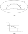
- Figure 1 is a schematic representation of a computing system 100 according to the invention.
- the computing system 100 comprises at least:
- the main processing module 110 is configured to manage the operation of the computing system 100.
- the main processing module 110 can be a microprocessor.
- the main processing module 110 can comprise an operating system, for example a Linux operating system.
- the main processing module 110 is configured to receive at least one computation task and to send the received computation task to the secondary processing module 120 for execution.
- the secondary processing module 120 is configured to execute the computation task received from the main processing module 110.
- the secondary processing module 120 can be a specific processing module dedicated to the computation of one or more specific computation tasks, for example an accelerator that is specialised to execute specific computation tasks faster than the main processing module 110.
- an accelerator that is specialised to execute specific computation tasks faster than the main processing module 110.
- it can be a Field-programmable Gate Array (FPGA), an Application-Specific Integrated Circuit (ASIC) or a Graphics Processing unit (GPU).
- FPGA Field-programmable Gate Array
- ASIC Application-Specific Integrated Circuit
- GPU Graphics Processing unit
- the first digital bus 140 is configured to transfer the computation task from the main processing module 110 to the secondary processing module 120.
- the first digital bus 140 is also configured to transfer from the secondary processing module 120 to the main processing module 110 the result of the computation task executed by the secondary processing module 120.
- the result can be any data type such as bytes, files, signals or instructions, or any combination thereof.
- the result type depends on the computation task type.
- the first digital bus 140 can be a high bandwidth data bus, for example a PCI-Express bus.
- the voltage regulation module 130 is configured to supply, via the output 131, voltage and current to the secondary processing module 120.
- the voltage at the output 131 is thereafter called output voltage.
- the voltage regulation module 130 can be a power supply unit made with a multi-phase voltage regulator controller and a plurality of power transistors. It can also include at least one digital component to implement more complex algorithms, for example it can implement one or more programmable logic units.
- the voltage regulation module 130 supplies the secondary processing module 120 with voltage according to a regulation law.
- the regulation law defines the voltage evolution as a function of at least one variable.
- the variable is for example the current flowing through the voltage regulation module 130, the temperature of the voltage regulation module 130 or a parameter linked to the imperfections of the voltage regulation module 130.
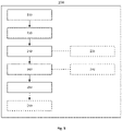
- Figure 2 is an example of the regulation law 132 used by the voltage regulation module 130 to adapt the output voltage in order to supply the secondary processing module 120 with a required current, that is the current needed by the secondary processing module 120 to execute the computation task.
- the horizontal axis corresponds to a variation range of current values in Ampere
- the vertical axis to a variation range of voltage values in Volt.
- the voltage value of the regulation law 132 is comprised between a maximum voltage value Umax and a minimum voltage value Umin and the current value is limited by a maximum current limit Imax.
- the regulation law 132 can either be a linear law, as represented in Figure 2 , or a non-linear law.
- the second digital bus 150 is configured to transfer at least one regulation parameter from the main processing module 110 to the voltage regulation module 130.
- the at least one regulation parameter is for example a maximum current limit or a temperature.
- the second digital bus 150 can also be configured to transfer at least one voltage value and at least one current value from the voltage regulation module 130 to the main processing module 110, said voltage and current value being measured at the output 131 of the voltage regulation module 130.
- the second digital bus 150 can be an Inter-Integrated Circuit (I2C) digital bus or any other bidirectional digital bus.
- I2C Inter-Integrated Circuit
- the computing system 100 can comprise at least one storage device connected to the main processing module 110.
- the storage device can be a non-volatile memory device such as a hard drive disk or a USB storage device, or a volatile memory storage such as a Random-Access Memory.
- the computing system 100 can comprise a network connection, for example it can be a wired connection, such as an Ethernet connection.
- the computing system can comprise a display device, such as monitor or a screen.
- the computing system 100 can also comprise a user interface, such as a keyboard, a mouse, a touchscreen or any combination thereof.
- a user interface such as a keyboard, a mouse, a touchscreen or any combination thereof.
- the main processing module 110, the secondary processing module 120 and the voltage regulation module 130 are embedded on a same board.
- the main processing module 110 is embedded on a first board and the secondary processing module 120, and preferentially the voltage regulation module 130, are embedded on a second board.
- the secondary processing module 120 and the voltage regulation module 130 are then connected to the main processing module 110 via at least one external plug.
- the external plug is a wired connection plug such as Universal Serial Bus (USB) or Ethernet plug, or a wireless connection plug such as Bluetooth or Wifi plug.
- the computing system 100 is comprised in a computer and the secondary processing module 120 is a graphics card of the computer.
- a second aspect of the invention concerns a method implemented by the computing system 100 according to the invention.
- Figure 3 is a synoptic scheme that synthetises the steps of the method 200 according to the invention.
- the main processing module 110 receives a computation task requested by a user or by an automatic process, and at least one regulation parameter related to the requested computation task.
- the at least one regulation parameter can either be given by a user or obtained by a development tool of the secondary processing module 120.
- the development tool is configured to estimate the at least one regulation parameter for a given requested computation task to be executed on the secondary processing module 120.
- the development tool can be made available by the secondary processing module provider 120.
- the main processing module 110 sends the at least one regulation parameter via the second digital bus 150 to the voltage regulation module 130.
- the voltage regulation module 130 adapts the regulation law 132 according to the received at least one regulation parameter and adjusts the output voltage according to the adapted regulation law 132.
- adjustment of the output voltage is meant modifying the voltage value supplied to the secondary processing module 120 to comply with the current required by the secondary processing module 120 to operate, indicated by the at least one regulation parameter received.
- the voltage regulation module 130 can preferentially adapt the regulation law 132 by modifying the offset of the regulation law 132.
- the offset can be the intercept with the vertical axis of the curve of the regulation law 132.
- the voltage regulation module 130 can adapt the regulation law 132 by modifying the slope of the regulation law 132. In the case the regulation law 132 is non-linear, the voltage regulation module 130 can adjust the regulation law 132 by modifying the first order derivative of the regulation law 132.
- the main processing module 110 monitors the voltage and the current measured at the output 131 of the voltage regulation module 130 via the second digital bus 150.
- the voltage and current at the output 131 of the voltage regulation module 130 are measured by the voltage regulation module 130 and sent to the main processing module 110 via the second digital bus 150.
- the voltage and current measured at the output 131 of the voltage regulation module 130 can be stored by the main processing module 110 in the storage device.
- a fourth step 240 the main processing module 110 sends the requested computation task received at the first step 210 to the secondary processing module 130 via the first bus 140 and the secondary processing module 130 executes the requested computation task.
- the main processing module 110 monitors, via the second digital bus 150, the voltage and the current measured at the output 131 of the voltage regulation module 130.
- the voltage and current at the output 131 of the voltage regulation module 130 are measured by the voltage regulation module 130 and sent to the main processing module 110 via the second digital bus 150.
- the voltage and current measured at the output 131 of the voltage regulation module 130 can be stored by the main processing module 110 in the storage device.
- a fifth step 250 the main processing module 110 collects, via the first digital bus 140, the result of the requested computation task executed by the secondary processing module 120.
- the main processing module 110 can provide the voltage regulation module 130 with at least one sleeping state regulation parameter to be applied to the secondary processing module 120 via the second digital bus 150.
- the at least one sleeping state regulation parameter corresponds to the at least one regulation parameter the secondary processing module 120 needs to enter a minimal working step.
- the at least one sleeping state regulation parameter can be given by the user, by the secondary processing module 120 provider or obtained by the development tool of the secondary processing module 120.
Landscapes
- Engineering & Computer Science (AREA)
- Theoretical Computer Science (AREA)
- Physics & Mathematics (AREA)
- General Engineering & Computer Science (AREA)
- General Physics & Mathematics (AREA)
- Power Sources (AREA)
Abstract
Description
- The technical field of the invention is the one of computing systems and more particularly of computing systems with an adjusted voltage regulation.
- The present invention concerns a computing system for adjusting the regulation of the voltage supplied to a secondary processing module executing computation tasks on request of a main processing module. The invention also concerns a method implemented by the computing system.
- Accelerators are processing units with specific internal architectures dedicated to the execution of specialized requested computation tasks. Most common accelerators are Field-Programmable Gate Arrays (FPGA), Application-Specific Integrated Circuits (ASIC) or Graphics Processing Units (GPU).
- An acceleration computing system, that is a computing system comprising an accelerator, further requires a main processing unit that provides the requested computation tasks to the accelerator, and a voltage regulation unit supplying electricity to the accelerator.
- Today, the voltage regulators implemented in acceleration computing systems are set up to supply current to the accelerator according to a regulation law. The regulation law indicates how the voltage at the output of the voltage regulator should be changed in order to supply a desired current, the voltage having to be comprised between a maximum voltage bound and a minimum voltage bound and the regulation law being defined based on a maximum current limit. The maximum voltage bound, the minimum voltage bound and the maximum current limit are imposed by the accelerator supplier.
- With latest silicon technologies, accelerators require a current supply that can vary a lot depending on the requested computation task and on their specific internal architecture. Accelerators are thus often not suitably supplied in current because the limitations imposed to the voltage regulator cannot always comply with the actual current the accelerator needs to properly work, which induces accelerator malfunctions.
- Another drawback is that the voltage regulator cannot anticipate the current the accelerator will need to execute the requested computation task. Because the voltage regulator can only supply the accelerator with voltage according to the regulation law, the voltage regulator can fall below the minimum voltage bound needed for the accelerator to properly work, in case of higher current than expected.
- Moreover, the voltage regulator can only measure the current flowing through the accelerator at the present time. and can therefore not anticipate the future accelerator current needs. It therefore induces a latency when a costly requested computation task is sent to the accelerator while this latter was at rest.
- Finally, when the current needed by the accelerator is lower than the maximum current limit, the voltage regulator often supplies an output voltage higher than needed in order to anticipate further current increase due to new requested computation tasks that may be executed. Then, the accelerator works below optimal energy efficiency as soon as maximum current is not used.
- Therefore, there is a need for an adapted voltage regulation in an acceleration computing system to supply optimal current and voltage to the accelerator.
- An object of the invention is to get an acceleration computing system wherein the voltage regulation supplied to the accelerator is optimized.
- A first aspect of the invention concerns a computing system for adjusting voltage regulation comprising:
- A main processing module configured to manage the operation of the computing system;
- A secondary processing module configured to execute requested computation tasks sent by the main processing module;
- A voltage regulation module comprising an output connected to the secondary processing module and configured to regulate the output voltage according to a regulation law defining a value for the output voltage as a function of at least one regulation parameter;
- A first digital bus connecting the main processing module and the secondary processing module, configured to transfer at least one requested computation task from the main processing module to the secondary processing module and to transfer at least one result of the requested computation task from the secondary processing module to the main processing module;
the computing system including: - A second digital bus connecting the voltage regulation module and the main processing module, configured to transfer the at least one regulation parameter depending on the requested computation task from the main processing module to the voltage regulation module.
- Thanks to the invention, the main processing module is able to communicate with the voltage regulation module via the second digital bus. Prior to the execution of a computation task by the secondary processing module, the main processing module can thus send at least one regulation parameter related to the computation task to the voltage regulation module in order to reach the secondary processing module maximum current without voltage drop under the specified minimum voltage bound. The current supplied by the voltage regulation module is therefore optimized for the computation task to be executed by the secondary processing module, which increases the computation performances of the secondary processing module. It also avoids under or overvoltage in the secondary processing module and therefore secondary processing module malfunctions.
- A side advantage of the invention is to induce minimal effort in secondary processing module software optimization to reduce energy consumption, thanks to the adjustment being achieved by the voltage regulation module in collaboration with the main processing module.
- Another advantage of the invention is that the voltage regulation module can supply an overvoltage value for a short duration which was not the case in the prior art. In fact, it happens that an optimal regulation may require exceeding the maximum voltage limit during a short period. As a matter of fact, the probability of computation errors is lower, or even neglectable, when the voltage is higher than specified, compared to when the voltage is under the minimal value.
- According to one embodiment, the at least one regulation parameter is a maximum current limit.
- The voltage regulation module can then adjust the current supplied to the secondary processing module according to the received maximum current limit.
- According to another embodiment, the second digital bus is further configured to transfer at least one voltage value and at least one current value from the voltage regulation module to the main processing module, said voltage value and said current value being measured at the output of the voltage regulation module.
- Thanks to this embodiment, the main processing module can monitor the voltage and current values supplied by the voltage regulation module to the secondary processing module. For example, the main processing module can monitor the voltage and current values to know when the voltage regulation module has completed the adjustment of the voltage regulation. For example, the main processing module can also monitor the voltage and current values during the execution of the requested computation task to know if the adjusted voltage is optimal with respect to the current needed for the execution of the requested computation task.
- According to a first alternative compatible with the previous embodiment, the main processing module and the secondary processing module are embedded on a same board.
- According to a second alternative compatible with the previous embodiment, the main processing module is embedded on a first board, and the second processing module and the voltage regulation module are embedded on a second board, the secondary processing module and the voltage regulation module being connected to the main processing module via at least one external plug.
- According to one embodiment compatible with the previous embodiment and alternatives, the secondary processing module is an accelerator
- Thanks to this embodiment, the secondary processing module is a specialized computing architecture dedicated to the execution of one specific task with higher performances than a regular processing module, such as a microprocessor, for example a Field-programmable gate array (FPGA), an Application-Specific integrated circuit (ASIC) or a Graphics processing unit (GPU).
- Another aspect of the invention concerns a method implemented by the computing system according to the invention comprising the following steps:
- Reception by the main processing module of a requested computation task and of at least one regulation parameter related to the requested computation task;
- Sending by the main processing module via the second digital bus to the voltage regulation module of at the least one regulation parameter;
- Adaptation by the voltage regulation module of the regulation law according to the at least one regulation parameter and adjustment by the voltage regulation module of the output voltage according to the adapted regulation law;
- Sending by the main processing module via the first digital bus to the secondary processing module of the requested computation task and execution by the secondary processing module of the requested computation task;
- Collection via the first digital bus by the main processing module of the result of the requested computation task completed by the secondary processing module.
- Thanks to this method, the main processing module is able to provide at least one appropriate regulation parameter to the voltage regulation module depending on the requested computation task the secondary processing module has to execute. The voltage regulation module is then able to adjust its regulation law according to the at least one regulation parameter received and can then supply the adequate current to the secondary processing module. Consequently, the secondary processing module can process the requested computation task with a suitable current supply, without over or under current and voltage consumption.
- According to one embodiment, the at least one regulation parameter is given by a user or is obtained by a development tool of the secondary processing module, said development tool being configured to estimate the regulation parameter for a given requested computation task to be executed on the secondary processing module.
- According to one embodiment compatible with the previous embodiment, the method according to the invention further comprises a sleeping state step after the collection step wherein the main processing module provides to the voltage regulation module via the second digital bus at least one sleeping state regulation parameter to be applied to the secondary processing module, said at least one sleeping state regulation parameter corresponding to the at least one regulation parameter the secondary processing module needs to enter a minimal working state.
- Thanks to this embodiment, the current supplied to the secondary processing module is adjusted in order to reduce the energy consumption of the computing system when no computation task is to be executed. The at least one regulation parameter provided by the main processing module to the voltage regulation module then corresponds to the at least one regulation parameter needed for the secondary processing module to enter a minimum working state corresponding to a minimal voltage allowing a resumption of activity of the secondary processing module without exceeding the voltage limits.
- According to one embodiment compatible with the previous embodiments, the regulation law of the voltage regulation module is either a linear law or a non-linear law.
- According to one embodiment compatible with the previous embodiments, the method according to the invention further comprises a first monitoring step during the adjustment step, wherein the main processing module monitors the voltage and the current measured at the output of the voltage regulator module via the second digital bus.
- Thanks to this embodiment, the main processing module knows when the adjustment of the regulation law by the voltage regulation module is done, so that the requested computation task can be sent to the secondary processing module.
- According to one embodiment compatible with the previous embodiments, the method according to the invention further comprises a second monitoring step during the execution step, wherein the main processing module monitors, via the second digital bus, the voltage and the current measured at the output of the voltage regulation module.
- Thanks to this embodiment, the main processing module can therefore know when the requested computation task is done to retrieve the result of the requested computation task.
- According to one embodiment compatible with the previous embodiments, the voltage and current values measured at the output of the regulation module are stored by the main processing module.
- Thanks to this embodiment, the voltage and current values can be used to forecast the current needed for further requested computation tasks similar to at least one previously executed computation task.
- The invention and its various applications will be better understood by reading the following description and examining the accompanying figures.
- The figures are presented for information purposes only and in no way limit the invention.
-
Figure 1 schematically illustrates a computing system according to the invention. -
Figure 2 provides an exemplary regulation law used in a third step of a method according to the invention. -
Figure 3 is a synoptic scheme illustrating the steps of the method according to the invention. - Some embodiments of devices and methods in accordance with embodiments of the present invention are now described, by way of example only, and with reference to the accompanying drawings. The description is to be regarded as illustrative in nature and not as restrictive.
- A first aspect of the invention concerns a computing system for adjusting voltage regulation.
-
Figure 1 is a schematic representation of acomputing system 100 according to the invention. - The
computing system 100 comprises at least: - A
main processing module 110; - A
secondary processing module 120; - A
voltage regulation module 130 having anoutput 131 connected to thesecondary processing module 120; - A first
digital bus 140 connecting themain processing module 110 and thesecondary processing module 120; - A second
digital bus 150 connecting thevoltage regulation module 130 and themain processing module 110. - The
main processing module 110 is configured to manage the operation of thecomputing system 100. - The
main processing module 110 can be a microprocessor. - The
main processing module 110 can comprise an operating system, for example a Linux operating system. - The
main processing module 110 is configured to receive at least one computation task and to send the received computation task to thesecondary processing module 120 for execution. - The
secondary processing module 120 is configured to execute the computation task received from themain processing module 110. - The
secondary processing module 120 can be a specific processing module dedicated to the computation of one or more specific computation tasks, for example an accelerator that is specialised to execute specific computation tasks faster than themain processing module 110. For example, it can be a Field-programmable Gate Array (FPGA), an Application-Specific Integrated Circuit (ASIC) or a Graphics Processing unit (GPU). - The first
digital bus 140 is configured to transfer the computation task from themain processing module 110 to thesecondary processing module 120. - The first
digital bus 140 is also configured to transfer from thesecondary processing module 120 to themain processing module 110 the result of the computation task executed by thesecondary processing module 120. - The result can be any data type such as bytes, files, signals or instructions, or any combination thereof. The result type depends on the computation task type.
- The first
digital bus 140 can be a high bandwidth data bus, for example a PCI-Express bus. - The
voltage regulation module 130 is configured to supply, via theoutput 131, voltage and current to thesecondary processing module 120. - The voltage at the
output 131 is thereafter called output voltage. - The
voltage regulation module 130 can be a power supply unit made with a multi-phase voltage regulator controller and a plurality of power transistors. It can also include at least one digital component to implement more complex algorithms, for example it can implement one or more programmable logic units. - The
voltage regulation module 130 supplies thesecondary processing module 120 with voltage according to a regulation law. The regulation law defines the voltage evolution as a function of at least one variable. - The variable is for example the current flowing through the
voltage regulation module 130, the temperature of thevoltage regulation module 130 or a parameter linked to the imperfections of thevoltage regulation module 130. -
Figure 2 is an example of theregulation law 132 used by thevoltage regulation module 130 to adapt the output voltage in order to supply thesecondary processing module 120 with a required current, that is the current needed by thesecondary processing module 120 to execute the computation task. - In
Figure 2 , the horizontal axis corresponds to a variation range of current values in Ampere, and the vertical axis to a variation range of voltage values in Volt. - The voltage value of the
regulation law 132 is comprised between a maximum voltage value Umax and a minimum voltage value Umin and the current value is limited by a maximum current limit Imax. - The
regulation law 132 can either be a linear law, as represented inFigure 2 , or a non-linear law. - The second
digital bus 150 is configured to transfer at least one regulation parameter from themain processing module 110 to thevoltage regulation module 130. - The at least one regulation parameter is for example a maximum current limit or a temperature.
- The second
digital bus 150 can also be configured to transfer at least one voltage value and at least one current value from thevoltage regulation module 130 to themain processing module 110, said voltage and current value being measured at theoutput 131 of thevoltage regulation module 130. - The second
digital bus 150 can be an Inter-Integrated Circuit (I2C) digital bus or any other bidirectional digital bus. - The
computing system 100 can comprise at least one storage device connected to themain processing module 110. - The storage device can be a non-volatile memory device such as a hard drive disk or a USB storage device, or a volatile memory storage such as a Random-Access Memory.
- The
computing system 100 can comprise a network connection, for example it can be a wired connection, such as an Ethernet connection. - The computing system can comprise a display device, such as monitor or a screen.
- The
computing system 100 can also comprise a user interface, such as a keyboard, a mouse, a touchscreen or any combination thereof. - According to a first embodiment, the
main processing module 110, thesecondary processing module 120 and thevoltage regulation module 130 are embedded on a same board. - According to a second embodiment, the
main processing module 110 is embedded on a first board and thesecondary processing module 120, and preferentially thevoltage regulation module 130, are embedded on a second board. Thesecondary processing module 120 and thevoltage regulation module 130 are then connected to themain processing module 110 via at least one external plug. For example, the external plug is a wired connection plug such as Universal Serial Bus (USB) or Ethernet plug, or a wireless connection plug such as Bluetooth or Wifi plug. - In a preferred embodiment of the invention, the
computing system 100 is comprised in a computer and thesecondary processing module 120 is a graphics card of the computer. - A second aspect of the invention concerns a method implemented by the
computing system 100 according to the invention. -
Figure 3 is a synoptic scheme that synthetises the steps of themethod 200 according to the invention. - The mandatory steps are indicated by rectangle with solid lines and the optional steps are indicated by rectangle with dashed lines.
- In a
first step 210, themain processing module 110 receives a computation task requested by a user or by an automatic process, and at least one regulation parameter related to the requested computation task. - The at least one regulation parameter can either be given by a user or obtained by a development tool of the
secondary processing module 120. The development tool is configured to estimate the at least one regulation parameter for a given requested computation task to be executed on thesecondary processing module 120. - The development tool can be made available by the secondary
processing module provider 120. - In a
second step 220, themain processing module 110 sends the at least one regulation parameter via the seconddigital bus 150 to thevoltage regulation module 130. - In a
third step 230, thevoltage regulation module 130 adapts theregulation law 132 according to the received at least one regulation parameter and adjusts the output voltage according to the adaptedregulation law 132. - By adjustment of the output voltage is meant modifying the voltage value supplied to the
secondary processing module 120 to comply with the current required by thesecondary processing module 120 to operate, indicated by the at least one regulation parameter received. - The
voltage regulation module 130 can preferentially adapt theregulation law 132 by modifying the offset of theregulation law 132. The offset can be the intercept with the vertical axis of the curve of theregulation law 132. - In the case the
regulation law 132 is linear, thevoltage regulation module 130 can adapt theregulation law 132 by modifying the slope of theregulation law 132. In the case theregulation law 132 is non-linear, thevoltage regulation module 130 can adjust theregulation law 132 by modifying the first order derivative of theregulation law 132. - In a sub-step 231 of the
third step 230, themain processing module 110 monitors the voltage and the current measured at theoutput 131 of thevoltage regulation module 130 via the seconddigital bus 150. - The voltage and current at the
output 131 of thevoltage regulation module 130 are measured by thevoltage regulation module 130 and sent to themain processing module 110 via the seconddigital bus 150. - During
sub-step 231, the voltage and current measured at theoutput 131 of thevoltage regulation module 130 can be stored by themain processing module 110 in the storage device. - In a
fourth step 240, themain processing module 110 sends the requested computation task received at thefirst step 210 to thesecondary processing module 130 via thefirst bus 140 and thesecondary processing module 130 executes the requested computation task. - In a sub-step 241 of the
fourth step 240, themain processing module 110 monitors, via the seconddigital bus 150, the voltage and the current measured at theoutput 131 of thevoltage regulation module 130. - The voltage and current at the
output 131 of thevoltage regulation module 130 are measured by thevoltage regulation module 130 and sent to themain processing module 110 via the seconddigital bus 150. - During
sub-step 241, the voltage and current measured at theoutput 131 of thevoltage regulation module 130 can be stored by themain processing module 110 in the storage device. - In a
fifth step 250, themain processing module 110 collects, via the firstdigital bus 140, the result of the requested computation task executed by thesecondary processing module 120. - In a
sixth step 260, themain processing module 110 can provide thevoltage regulation module 130 with at least one sleeping state regulation parameter to be applied to thesecondary processing module 120 via the seconddigital bus 150. - The at least one sleeping state regulation parameter corresponds to the at least one regulation parameter the
secondary processing module 120 needs to enter a minimal working step. - The at least one sleeping state regulation parameter can be given by the user, by the
secondary processing module 120 provider or obtained by the development tool of thesecondary processing module 120.
Claims (13)
- A computing system (100) for adjusting voltage regulation comprising:• A main processing module (110) configured to manage the operation of the computing system (100);• A secondary processing module (120) configured to execute requested computation tasks sent by the main processing module (110);• A voltage regulation module (130) comprising an output (131) connected to the secondary processing module (120) and configured to regulate the output voltage according to a regulation law (132) defining a value for the output voltage as a function of at least one regulation parameter;• A first digital bus (140) connecting the main processing module (110) and the secondary processing module (120), configured to transfer at least one requested computation task from the main processing module (110) to the secondary processing module (120) and to transfer at least one result of the requested computation task from the secondary processing module (120) to the main processing module (110);
the computing system (100) being characterized in that it includes:• A second digital bus (150) connecting the voltage regulation module (130) and the main processing module (110), configured to transfer the at least one regulation parameter depending on the requested computation task from the main processing module (110) to the voltage regulation module (130). - A method according to claim 1, wherein the at least one regulation parameter is a maximum current limit.
- A computing system (100) according to any of the preceding claims, wherein the second digital bus (150) is further configured to transfer at least one voltage value and at least one current value from the voltage regulation module (130) to the main processing module (110), said voltage value and said current value being measured at the output (131) of the voltage regulation module (130).
- A computing system (100) according to any of the preceding claims, wherein the main processing module (110), the secondary processing module (120) and the voltage regulation module (130) are embedded on a same board.
- A computing system (100) according to any one of claims 1 to 3, wherein the main processing module (110) is embedded on a first board, and the secondary processing module (120) and the voltage regulation module (130) are embedded on a second board, the secondary processing module (120) and the voltage regulation module (130) being connected to the main processing module (110) via at least one external plug.
- A computing system (100) according to any of the preceding claims, wherein the secondary processing module (120) is an accelerator.
- A method (200) implemented by the computing system (100) according to any one of the preceding claims, characterized in that it comprises the following steps:• Reception (210) by the main processing module (110) of a requested computation task and of at least one regulation parameter related to the requested computation task;• Sending (220) by the main processing module (110) via the second digital bus (150) to the voltage regulation module (130) of the at least one regulation parameter;• Adaptation (230) by the voltage regulation module (130) of the regulation law (132) according to the at least one regulation parameter and adjustment by the voltage regulation module (130) of the output voltage according to the adapted regulation law (132);• Sending (240) by the main processing module (110) via the first digital bus (140) to the secondary processing module (120) of the requested computation task and execution by the secondary processing module (120) of the requested computation task;• Collection (250) via the first digital bus (140) by the main processing module (110) of the result of the requested computation task completed by the secondary processing module (120).
- A method according to claim 7, wherein said at least one regulation parameter is given by a user or is obtained by a development tool of the secondary processing module (120), said development tool being configured to estimate the regulation parameter for a given requested computation task to be executed on the secondary processing module (120).
- A method according to any one of claim 7 or 8, further comprising a sleeping state step (260) after the collection step (250), wherein the main processing module (110) provides to the voltage regulation module (130) via the second digital bus (150) at least one sleeping state regulation parameter to be applied to the secondary processing module (120), said at least one sleeping state regulation parameter corresponding to the at least one regulation parameter the secondary processing module (120) needs to enter a minimal working state.
- A method according to any one of claims 7 to 9, wherein the regulation law (132) is either a linear or a non-linear law.
- A method according to any one of claims 7 to 10, further comprising a first monitoring step (231) during the adjustment step (230), wherein the main processing module (110) monitors the voltage and the current measured at the output (131) of the voltage regulator module (130) via the second digital bus (150).
- A method according to any one of claims 7 to 11, further comprising a second monitoring step (241) during the execution step (240), wherein the main processing module (110) monitors, via the second digital bus (150), the voltage and the current measured at the output (131) of the voltage regulation module (130).
- A method according to claim 11 or 12, wherein the voltage and the current measured at the output of the voltage regulation module (130) are stored by the main processing module (110).
Priority Applications (2)
| Application Number | Priority Date | Filing Date | Title |
|---|---|---|---|
| EP21306355.5A EP4160355A1 (en) | 2021-09-30 | 2021-09-30 | Computing system and method for adjusting voltage regulation |
| US17/957,021 US12026035B2 (en) | 2021-09-30 | 2022-09-30 | Computing system and method for adjusting voltage regulation |
Applications Claiming Priority (1)
| Application Number | Priority Date | Filing Date | Title |
|---|---|---|---|
| EP21306355.5A EP4160355A1 (en) | 2021-09-30 | 2021-09-30 | Computing system and method for adjusting voltage regulation |
Publications (1)
| Publication Number | Publication Date |
|---|---|
| EP4160355A1 true EP4160355A1 (en) | 2023-04-05 |
Family
ID=78500568
Family Applications (1)
| Application Number | Title | Priority Date | Filing Date |
|---|---|---|---|
| EP21306355.5A Pending EP4160355A1 (en) | 2021-09-30 | 2021-09-30 | Computing system and method for adjusting voltage regulation |
Country Status (2)
| Country | Link |
|---|---|
| US (1) | US12026035B2 (en) |
| EP (1) | EP4160355A1 (en) |
Citations (3)
| Publication number | Priority date | Publication date | Assignee | Title |
|---|---|---|---|---|
| US7421604B1 (en) * | 2005-07-25 | 2008-09-02 | Nvidia Corporation | Advanced voltage regulation using feed-forward load information |
| WO2019032207A1 (en) * | 2017-08-10 | 2019-02-14 | Microsoft Technology Licensing, Llc | Load line regulation via clamping voltage |
| US20200050920A1 (en) * | 2018-08-09 | 2020-02-13 | Nvidia Corporation | Techniques for efficiently operating a processing system based on energy characteristics of instructions and machine learning |
Family Cites Families (2)
| Publication number | Priority date | Publication date | Assignee | Title |
|---|---|---|---|---|
| US6697952B1 (en) * | 2000-07-24 | 2004-02-24 | Dell Products, L.P. | Margining processor power supply |
| US9430007B2 (en) * | 2014-04-24 | 2016-08-30 | Lenovo Enterprise Solutions (Singapore) Pte. Ltd. | Voltage regulator stress reducing system |
-
2021
- 2021-09-30 EP EP21306355.5A patent/EP4160355A1/en active Pending
-
2022
- 2022-09-30 US US17/957,021 patent/US12026035B2/en active Active
Patent Citations (3)
| Publication number | Priority date | Publication date | Assignee | Title |
|---|---|---|---|---|
| US7421604B1 (en) * | 2005-07-25 | 2008-09-02 | Nvidia Corporation | Advanced voltage regulation using feed-forward load information |
| WO2019032207A1 (en) * | 2017-08-10 | 2019-02-14 | Microsoft Technology Licensing, Llc | Load line regulation via clamping voltage |
| US20200050920A1 (en) * | 2018-08-09 | 2020-02-13 | Nvidia Corporation | Techniques for efficiently operating a processing system based on energy characteristics of instructions and machine learning |
Also Published As
| Publication number | Publication date |
|---|---|
| US20230098209A1 (en) | 2023-03-30 |
| US12026035B2 (en) | 2024-07-02 |
Similar Documents
| Publication | Publication Date | Title |
|---|---|---|
| US20240295911A1 (en) | Synchronous power state control scheme for multi-chip integrated power management solution in embedded systems | |
| JPWO2015019541A1 (en) | Power system stabilization method, power system stabilization system, and power supply device | |
| US8145921B2 (en) | Multi-regulator power supply chip with common control bus | |
| WO2019075980A1 (en) | Thread adjustment method and terminal thereof | |
| EP1612910A1 (en) | On-board power supply monitor and power control system | |
| JP7280556B2 (en) | Negawatt trading support device and negawatt trading method | |
| CN104081312A (en) | Voltage regulator control system | |
| CN115066659B (en) | Machine learning device, computer device, control system, and machine learning method | |
| JP7474368B2 (en) | Power management system, power management server, control device, and power management method | |
| JP2004531787A (en) | System for controlling or regulating | |
| US12026035B2 (en) | Computing system and method for adjusting voltage regulation | |
| US20170097674A1 (en) | Power Management for Datacenter Power Architectures | |
| US10038328B2 (en) | Digital temperature control for power supply devices | |
| KR101052284B1 (en) | Power Sequence / Clock Timing Controls | |
| EP3159769A1 (en) | Pulse-width modulation voltage identification interface | |
| US12393888B2 (en) | Multi-objective electric vehicle charging scheduler with configurable objective hierarchy | |
| CN111869043B (en) | Energy management based on multiple signals | |
| US20070050648A1 (en) | System and method for communication between a controller and a power supply using a communication interface | |
| JP4972522B2 (en) | Data processing system | |
| CN116931707A (en) | System-on-chip, dynamic adjustment method and chip system | |
| CN119253694B (en) | Internal resistance adjusting method and system of energy storage equipment, computer equipment and related device | |
| US10401946B1 (en) | Power delivery for processing units | |
| WO2024188467A1 (en) | Systems and methods for controlling charging of electric vehicles for electric power grid services | |
| CN118120127B (en) | Charge and discharge control method and charge and discharge control device | |
| JP5267099B2 (en) | Fieldbus type electromagnetic flow meter |
Legal Events
| Date | Code | Title | Description |
|---|---|---|---|
| PUAI | Public reference made under article 153(3) epc to a published international application that has entered the european phase |
Free format text: ORIGINAL CODE: 0009012 |
|
| STAA | Information on the status of an ep patent application or granted ep patent |
Free format text: STATUS: THE APPLICATION HAS BEEN PUBLISHED |
|
| AK | Designated contracting states |
Kind code of ref document: A1 Designated state(s): AL AT BE BG CH CY CZ DE DK EE ES FI FR GB GR HR HU IE IS IT LI LT LU LV MC MK MT NL NO PL PT RO RS SE SI SK SM TR |
|
| STAA | Information on the status of an ep patent application or granted ep patent |
Free format text: STATUS: REQUEST FOR EXAMINATION WAS MADE |
|
| 17P | Request for examination filed |
Effective date: 20231004 |
|
| RBV | Designated contracting states (corrected) |
Designated state(s): AL AT BE BG CH CY CZ DE DK EE ES FI FR GB GR HR HU IE IS IT LI LT LU LV MC MK MT NL NO PL PT RO RS SE SI SK SM TR |
|
| STAA | Information on the status of an ep patent application or granted ep patent |
Free format text: STATUS: EXAMINATION IS IN PROGRESS |
|
| 17Q | First examination report despatched |
Effective date: 20250214 |