EP4160314A1 - Procédé de mesure d'au moins une cible sur un substrat - Google Patents
Procédé de mesure d'au moins une cible sur un substrat Download PDFInfo
- Publication number
- EP4160314A1 EP4160314A1 EP21200798.3A EP21200798A EP4160314A1 EP 4160314 A1 EP4160314 A1 EP 4160314A1 EP 21200798 A EP21200798 A EP 21200798A EP 4160314 A1 EP4160314 A1 EP 4160314A1
- Authority
- EP
- European Patent Office
- Prior art keywords
- targets
- target
- parameter
- interest
- sub
- Prior art date
- Legal status (The legal status is an assumption and is not a legal conclusion. Google has not performed a legal analysis and makes no representation as to the accuracy of the status listed.)
- Withdrawn
Links
- 238000000034 method Methods 0.000 title claims abstract description 109
- 239000000758 substrate Substances 0.000 title claims abstract description 104
- 238000005259 measurement Methods 0.000 claims abstract description 123
- 238000012937 correction Methods 0.000 claims abstract description 49
- 230000000694 effects Effects 0.000 claims abstract description 16
- 230000005855 radiation Effects 0.000 claims description 46
- 230000008569 process Effects 0.000 claims description 40
- 230000000737 periodic effect Effects 0.000 claims description 30
- 230000001419 dependent effect Effects 0.000 claims description 10
- 230000008859 change Effects 0.000 claims description 3
- 238000005286 illumination Methods 0.000 description 20
- 238000000059 patterning Methods 0.000 description 19
- 230000003287 optical effect Effects 0.000 description 17
- 239000010410 layer Substances 0.000 description 14
- 210000001747 pupil Anatomy 0.000 description 10
- 238000004590 computer program Methods 0.000 description 9
- 238000004519 manufacturing process Methods 0.000 description 9
- 238000013461 design Methods 0.000 description 8
- 238000007689 inspection Methods 0.000 description 8
- 238000001228 spectrum Methods 0.000 description 8
- 238000012545 processing Methods 0.000 description 7
- 238000001459 lithography Methods 0.000 description 6
- 230000006870 function Effects 0.000 description 4
- 238000012544 monitoring process Methods 0.000 description 4
- 230000001052 transient effect Effects 0.000 description 4
- 239000002131 composite material Substances 0.000 description 3
- 238000003384 imaging method Methods 0.000 description 3
- 238000007654 immersion Methods 0.000 description 3
- 239000007788 liquid Substances 0.000 description 3
- 230000010287 polarization Effects 0.000 description 3
- 239000004065 semiconductor Substances 0.000 description 3
- 238000004088 simulation Methods 0.000 description 3
- 239000002356 single layer Substances 0.000 description 3
- 238000012935 Averaging Methods 0.000 description 2
- 238000004458 analytical method Methods 0.000 description 2
- 238000004140 cleaning Methods 0.000 description 2
- 230000003750 conditioning effect Effects 0.000 description 2
- 230000007547 defect Effects 0.000 description 2
- 238000010586 diagram Methods 0.000 description 2
- 238000009826 distribution Methods 0.000 description 2
- 230000005670 electromagnetic radiation Effects 0.000 description 2
- 238000005516 engineering process Methods 0.000 description 2
- 230000003993 interaction Effects 0.000 description 2
- 238000012417 linear regression Methods 0.000 description 2
- 238000013507 mapping Methods 0.000 description 2
- 238000013178 mathematical model Methods 0.000 description 2
- 238000005457 optimization Methods 0.000 description 2
- 238000000206 photolithography Methods 0.000 description 2
- 230000009467 reduction Effects 0.000 description 2
- 239000007787 solid Substances 0.000 description 2
- 238000012369 In process control Methods 0.000 description 1
- 238000013459 approach Methods 0.000 description 1
- 238000004364 calculation method Methods 0.000 description 1
- 230000000295 complement effect Effects 0.000 description 1
- 150000001875 compounds Chemical class 0.000 description 1
- 238000001514 detection method Methods 0.000 description 1
- 230000009977 dual effect Effects 0.000 description 1
- 239000002355 dual-layer Substances 0.000 description 1
- 238000005530 etching Methods 0.000 description 1
- 238000001914 filtration Methods 0.000 description 1
- 238000000671 immersion lithography Methods 0.000 description 1
- 238000010965 in-process control Methods 0.000 description 1
- 239000004973 liquid crystal related substance Substances 0.000 description 1
- 230000005381 magnetic domain Effects 0.000 description 1
- 239000000463 material Substances 0.000 description 1
- 238000000691 measurement method Methods 0.000 description 1
- 230000015654 memory Effects 0.000 description 1
- 238000012986 modification Methods 0.000 description 1
- 230000004048 modification Effects 0.000 description 1
- 238000003909 pattern recognition Methods 0.000 description 1
- 230000000704 physical effect Effects 0.000 description 1
- 238000002360 preparation method Methods 0.000 description 1
- 238000007639 printing Methods 0.000 description 1
- 238000004886 process control Methods 0.000 description 1
- 238000007493 shaping process Methods 0.000 description 1
- 239000002904 solvent Substances 0.000 description 1
- 230000003068 static effect Effects 0.000 description 1
- 239000010409 thin film Substances 0.000 description 1
- 238000012546 transfer Methods 0.000 description 1
- 238000012795 verification Methods 0.000 description 1
- XLYOFNOQVPJJNP-UHFFFAOYSA-N water Substances O XLYOFNOQVPJJNP-UHFFFAOYSA-N 0.000 description 1
- 229910052724 xenon Inorganic materials 0.000 description 1
- FHNFHKCVQCLJFQ-UHFFFAOYSA-N xenon atom Chemical compound [Xe] FHNFHKCVQCLJFQ-UHFFFAOYSA-N 0.000 description 1
Images


Classifications
-
- G—PHYSICS
- G03—PHOTOGRAPHY; CINEMATOGRAPHY; ANALOGOUS TECHNIQUES USING WAVES OTHER THAN OPTICAL WAVES; ELECTROGRAPHY; HOLOGRAPHY
- G03F—PHOTOMECHANICAL PRODUCTION OF TEXTURED OR PATTERNED SURFACES, e.g. FOR PRINTING, FOR PROCESSING OF SEMICONDUCTOR DEVICES; MATERIALS THEREFOR; ORIGINALS THEREFOR; APPARATUS SPECIALLY ADAPTED THEREFOR
- G03F7/00—Photomechanical, e.g. photolithographic, production of textured or patterned surfaces, e.g. printing surfaces; Materials therefor, e.g. comprising photoresists; Apparatus specially adapted therefor
- G03F7/70—Microphotolithographic exposure; Apparatus therefor
- G03F7/70483—Information management; Active and passive control; Testing; Wafer monitoring, e.g. pattern monitoring
- G03F7/70605—Workpiece metrology
- G03F7/706843—Metrology apparatus
- G03F7/706845—Calibration, e.g. tool-to-tool calibration, beam alignment, spot position or focus
-
- G—PHYSICS
- G03—PHOTOGRAPHY; CINEMATOGRAPHY; ANALOGOUS TECHNIQUES USING WAVES OTHER THAN OPTICAL WAVES; ELECTROGRAPHY; HOLOGRAPHY
- G03F—PHOTOMECHANICAL PRODUCTION OF TEXTURED OR PATTERNED SURFACES, e.g. FOR PRINTING, FOR PROCESSING OF SEMICONDUCTOR DEVICES; MATERIALS THEREFOR; ORIGINALS THEREFOR; APPARATUS SPECIALLY ADAPTED THEREFOR
- G03F7/00—Photomechanical, e.g. photolithographic, production of textured or patterned surfaces, e.g. printing surfaces; Materials therefor, e.g. comprising photoresists; Apparatus specially adapted therefor
- G03F7/70—Microphotolithographic exposure; Apparatus therefor
- G03F7/70483—Information management; Active and passive control; Testing; Wafer monitoring, e.g. pattern monitoring
- G03F7/70605—Workpiece metrology
- G03F7/70616—Monitoring the printed patterns
- G03F7/70633—Overlay, i.e. relative alignment between patterns printed by separate exposures in different layers, or in the same layer in multiple exposures or stitching
-
- G—PHYSICS
- G03—PHOTOGRAPHY; CINEMATOGRAPHY; ANALOGOUS TECHNIQUES USING WAVES OTHER THAN OPTICAL WAVES; ELECTROGRAPHY; HOLOGRAPHY
- G03F—PHOTOMECHANICAL PRODUCTION OF TEXTURED OR PATTERNED SURFACES, e.g. FOR PRINTING, FOR PROCESSING OF SEMICONDUCTOR DEVICES; MATERIALS THEREFOR; ORIGINALS THEREFOR; APPARATUS SPECIALLY ADAPTED THEREFOR
- G03F7/00—Photomechanical, e.g. photolithographic, production of textured or patterned surfaces, e.g. printing surfaces; Materials therefor, e.g. comprising photoresists; Apparatus specially adapted therefor
- G03F7/70—Microphotolithographic exposure; Apparatus therefor
- G03F7/70483—Information management; Active and passive control; Testing; Wafer monitoring, e.g. pattern monitoring
- G03F7/70605—Workpiece metrology
- G03F7/70616—Monitoring the printed patterns
- G03F7/70641—Focus
-
- G—PHYSICS
- G03—PHOTOGRAPHY; CINEMATOGRAPHY; ANALOGOUS TECHNIQUES USING WAVES OTHER THAN OPTICAL WAVES; ELECTROGRAPHY; HOLOGRAPHY
- G03F—PHOTOMECHANICAL PRODUCTION OF TEXTURED OR PATTERNED SURFACES, e.g. FOR PRINTING, FOR PROCESSING OF SEMICONDUCTOR DEVICES; MATERIALS THEREFOR; ORIGINALS THEREFOR; APPARATUS SPECIALLY ADAPTED THEREFOR
- G03F7/00—Photomechanical, e.g. photolithographic, production of textured or patterned surfaces, e.g. printing surfaces; Materials therefor, e.g. comprising photoresists; Apparatus specially adapted therefor
- G03F7/70—Microphotolithographic exposure; Apparatus therefor
- G03F7/70483—Information management; Active and passive control; Testing; Wafer monitoring, e.g. pattern monitoring
- G03F7/70605—Workpiece metrology
- G03F7/70681—Metrology strategies
- G03F7/70683—Mark designs
Definitions
- the present invention relates to metrology applications in the manufacture of integrated circuits.
- a lithographic apparatus is a machine constructed to apply a desired pattern onto a substrate.
- a lithographic apparatus can be used, for example, in the manufacture of integrated circuits (ICs).
- a lithographic apparatus may, for example, project a pattern (also often referred to as "design layout" or "design") at a patterning device (e.g., a mask) onto a layer of radiation-sensitive material (resist) provided on a substrate (e.g., a wafer).
- a lithographic apparatus may use electromagnetic radiation.
- the wavelength of this radiation determines the minimum size of features which can be formed on the substrate. Typical wavelengths currently in use are 365 nm (i-line), 248 nm, 193 nm and 13.5 nm.
- a lithographic apparatus which uses extreme ultraviolet (EUV) radiation, having a wavelength within the range 4-20 nm, for example 6.7 nm or 13.5 nm, may be used to form smaller features on a substrate than a lithographic apparatus which uses, for example, radiation with a wavelength of 193 nm.
- EUV extreme ultraviolet
- Low-kl lithography may be used to process features with dimensions smaller than the classical resolution limit of a lithographic apparatus.
- k1 the more difficult it becomes to reproduce the pattern on the substrate that resembles the shape and dimensions planned by a circuit designer in order to achieve particular electrical functionality and performance.
- sophisticated fine-tuning steps may be applied to the lithographic projection apparatus and/or design layout.
- RET resolution enhancement techniques
- Metrology tools are used in many aspects of the IC manufacturing process, for example as alignment tools for proper positioning of a substrate prior to an exposure and scatterometry based tools for inspecting/measuring the exposed and/or etched product in process control; e.g., to measure overlay.
- a method of determining a correction for a measurement of at least one target on a substrate comprising one or more parameter of interest sensitive sub-targets which are each sensitive to a parameter of interest and one or more parameter of interest insensitive sub-targets which are substantially less sensitive or insensitive to the parameter of interest, the method comprising: obtaining a respective first measurement parameter value relating to each of said one or more parameter of interest sensitive sub-targets; obtaining a respective second measurement parameter value relating to each of said one or more parameter of interest insensitive sub-targets; and determining a correction for each said first measurement parameter value using said second measurement parameter values and/or detecting the presence of an effect likely to impact accuracy of first measurement parameter values from said second measurement parameter values.
- a substrate comprising: at least one target comprising one or more parameter of interest sensitive sub-targets which are each sensitive to a parameter of interest and one or more parameter of interest insensitive sub-targets which are substantially less sensitive or insensitive to the parameter of interest.
- the invention yet further provides a computer program product comprising machine-readable instructions for causing a processor to perform the method of the first aspect, and associated metrology apparatus.
- the terms "radiation” and “beam” are used to encompass all types of electromagnetic radiation, including ultraviolet radiation (e.g. with a wavelength of 365, 248, 193, 157 or 126 nm) and EUV (extreme ultra-violet radiation, e.g. having a wavelength in the range of about 5-100 nm).
- ultraviolet radiation e.g. with a wavelength of 365, 248, 193, 157 or 126 nm
- EUV extreme ultra-violet radiation
- reticle may be broadly interpreted as referring to a generic patterning device that can be used to endow an incoming radiation beam with a patterned cross-section, corresponding to a pattern that is to be created in a target portion of the substrate.
- the term “light valve” can also be used in this context.
- examples of other such patterning devices include a programmable mirror array and a programmable LCD array.
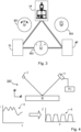
- FIG. 1 schematically depicts a lithographic apparatus LA or scanner (the two terms are used synonymously, although the concepts herein may also be applicable to stepper arrnagements) .
- the lithographic apparatus LA includes an illumination system (also referred to as illuminator) IL configured to condition a radiation beam B (e.g., UV radiation, DUV radiation or EUV radiation), a mask support (e.g., a mask table) MT constructed to support a patterning device (e.g., a mask) MA and connected to a first positioner PM configured to accurately position the patterning device MA in accordance with certain parameters, a substrate support (e.g., a wafer table) WT constructed to hold a substrate (e.g., a resist coated wafer) W and connected to a second positioner PW configured to accurately position the substrate support in accordance with certain parameters, and a projection system (e.g., a refractive projection lens system) PS configured to project a pattern imparted to the radiation beam B by
- the illumination system IL receives a radiation beam from a radiation source SO, e.g. via a beam delivery system BD.
- the illumination system IL may include various types of optical components, such as refractive, reflective, magnetic, electromagnetic, electrostatic, and/or other types of optical components, or any combination thereof, for directing, shaping, and/or controlling radiation.
- the illuminator IL may be used to condition the radiation beam B to have a desired spatial and angular intensity distribution in its cross section at a plane of the patterning device MA.
- projection system PS used herein should be broadly interpreted as encompassing various types of projection system, including refractive, reflective, catadioptric, anamorphic, magnetic, electromagnetic and/or electrostatic optical systems, or any combination thereof, as appropriate for the exposure radiation being used, and/or for other factors such as the use of an immersion liquid or the use of a vacuum. Any use of the term “projection lens” herein may be considered as synonymous with the more general term “projection system” PS.
- the lithographic apparatus LA may be of a type wherein at least a portion of the substrate may be covered by a liquid having a relatively high refractive index, e.g., water, so as to fill a space between the projection system PS and the substrate W - which is also referred to as immersion lithography. More information on immersion techniques is given in US6952253 , which is incorporated herein by reference.
- the lithographic apparatus LA may also be of a type having two or more substrate supports WT (also named “dual stage”).
- the substrate supports WT may be used in parallel, and/or steps in preparation of a subsequent exposure of the substrate W may be carried out on the substrate W located on one of the substrate support WT while another substrate W on the other substrate support WT is being used for exposing a pattern on the other substrate W.
- the lithographic apparatus LA may comprise a measurement stage.
- the measurement stage is arranged to hold a sensor and/or a cleaning device.
- the sensor may be arranged to measure a property of the projection system PS or a property of the radiation beam B.
- the measurement stage may hold multiple sensors.
- the cleaning device may be arranged to clean part of the lithographic apparatus, for example a part of the projection system PS or a part of a system that provides the immersion liquid.
- the measurement stage may move beneath the projection system PS when the substrate support WT is away from the projection system PS.
- the radiation beam B is incident on the patterning device, e.g. mask, MA which is held on the mask support MT, and is patterned by the pattern (design layout) present on patterning device MA. Having traversed the mask MA, the radiation beam B passes through the projection system PS, which focuses the beam onto a target portion C of the substrate W. With the aid of the second positioner PW and a position measurement system IF, the substrate support WT can be moved accurately, e.g., so as to position different target portions C in the path of the radiation beam B at a focused and aligned position.
- the patterning device e.g. mask, MA which is held on the mask support MT, and is patterned by the pattern (design layout) present on patterning device MA.
- the radiation beam B passes through the projection system PS, which focuses the beam onto a target portion C of the substrate W.
- the substrate support WT can be moved accurately, e.g., so as to position different target portions C in the path of the radiation beam B at a focused
- first positioner PM and possibly another position sensor may be used to accurately position the patterning device MA with respect to the path of the radiation beam B.
- Patterning device MA and substrate W may be aligned using mask alignment marks M1, M2 and substrate alignment marks PI, P2.
- substrate alignment marks PI, P2 as illustrated occupy dedicated target portions, they may be located in spaces between target portions.
- Substrate alignment marks PI, P2 are known as scribe-lane alignment marks when these are located between the target portions C.
- the lithographic apparatus LA may form part of a lithographic cell LC, also sometimes referred to as a lithocell or (litho)cluster, which often also includes apparatus to perform pre- and post-exposure processes on a substrate W.
- a lithographic cell LC also sometimes referred to as a lithocell or (litho)cluster
- these include spin coaters SC to deposit resist layers, developers DE to develop exposed resist, chill plates CH and bake plates BK, e.g. for conditioning the temperature of substrates W e.g. for conditioning solvents in the resist layers.
- a substrate handler, or robot, RO picks up substrates W from input/output ports I/O1, I/O2, moves them between the different process apparatus and delivers the substrates W to the loading bay LB of the lithographic apparatus LA.
- the devices in the lithocell which are often also collectively referred to as the track, are typically under the control of a track control unit TCU that in itself may be controlled by a supervisory control system SCS, which may also control the lithographic apparatus LA, e.g. via lithography control unit LACU.
- a supervisory control system SCS which may also control the lithographic apparatus LA, e.g. via lithography control unit LACU.
- inspection tools may be included in the lithocell LC. If errors are detected, adjustments, for example, may be made to exposures of subsequent substrates or to other processing steps that are to be performed on the substrates W, especially if the inspection is done before other substrates W of the same batch or lot are still to be exposed or processed.
- An inspection apparatus which may also be referred to as a metrology apparatus, is used to determine properties of the substrates W, and in particular, how properties of different substrates W vary or how properties associated with different layers of the same substrate W vary from layer to layer.
- the inspection apparatus may alternatively be constructed to identify defects on the substrate W and may, for example, be part of the lithocell LC, or may be integrated into the lithographic apparatus LA, or may even be a stand-alone device.
- the inspection apparatus may measure the properties on a latent image (image in a resist layer after the exposure), or on a semi-latent image (image in a resist layer after a post-exposure bake step PEB), or on a developed resist image (in which the exposed or unexposed parts of the resist have been removed), or even on an etched image (after a pattern transfer step such as etching).
- the patterning process in a lithographic apparatus LA is one of the most critical steps in the processing which requires high accuracy of dimensioning and placement of structures on the substrate W.
- three systems may be combined in a so called “holistic" control environment as schematically depicted in Fig. 3 .
- One of these systems is the lithographic apparatus LA which is (virtually) connected to a metrology tool MT (a second system) and to a computer system CL (a third system).
- the key of such "holistic" environment is to optimize the cooperation between these three systems to enhance the overall process window and provide tight control loops to ensure that the patterning performed by the lithographic apparatus LA stays within a process window.
- the process window defines a range of process parameters (e.g. dose, focus, overlay) within which a specific manufacturing process yields a defined result (e.g. a functional semiconductor device) - typically within which the process parameters in the lithographic process or patterning process are allowed to vary.
- the computer system CL may use (part of) the design layout to be patterned to predict which resolution enhancement techniques to use and to perform computational lithography simulations and calculations to determine which mask layout and lithographic apparatus settings achieve the largest overall process window of the patterning process (depicted in Fig. 3 by the double arrow in the first scale SC1).
- the resolution enhancement techniques are arranged to match the patterning possibilities of the lithographic apparatus LA.
- the computer system CL may also be used to detect where within the process window the lithographic apparatus LA is currently operating (e.g. using input from the metrology tool MT) to predict whether defects may be present due to e.g. sub-optimal processing (depicted in Fig. 3 by the arrow pointing "0" in the second scale SC2).
- the metrology tool MT may provide input to the computer system CL to enable accurate simulations and predictions, and may provide feedback to the lithographic apparatus LA to identify possible drifts, e.g. in a calibration status of the lithographic apparatus LA (depicted in Fig. 3 by the multiple arrows in the third scale SC3).
- metrology tools MT In lithographic processes, it is desirable to make frequently measurements of the structures created, e.g., for process control and verification. Tools to make such measurement are typically called metrology tools MT. Different types of metrology tools MT for making such measurements are known, including scanning electron microscopes or various forms of scatterometer metrology tools MT. Scatterometers are versatile instruments which allow measurements of the parameters of a lithographic process by having a sensor in the pupil or a conjugate plane with the pupil of the objective of the scatterometer, measurements usually referred as pupil based measurements, or by having the sensor in the image plane or a plane conjugate with the image plane, in which case the measurements are usually referred as image or field based measurements.
- Such scatterometers and the associated measurement techniques are further described in patent applications US20100328655 , US2011102753A1 , US20120044470A , US20110249244 , US20110026032 or EP1,628,164A , incorporated herein by reference in their entirety.
- Aforementioned scatterometers may measure gratings using light from soft x-ray and visible to near-IR wavelength range.
- the scatterometer MT is an angular resolved scatterometer.
- reconstruction methods may be applied to the measured signal to reconstruct or calculate properties of the grating.
- Such reconstruction may, for example, result from simulating interaction of scattered radiation with a mathematical model of the target arrangement and comparing the simulation results with those of a measurement. Parameters of the mathematical model are adjusted until the simulated interaction produces a diffraction pattern similar to that observed from the real target.
- the scatterometer MT is a spectroscopic scatterometer MT.
- the radiation emitted by a radiation source is directed onto the target and the reflected or scattered radiation from the target is directed to a spectrometer detector, which measures a spectrum (i.e. a measurement of intensity as a function of wavelength) of the specular reflected radiation. From this data, the structure or profile of the target giving rise to the detected spectrum may be reconstructed, e.g. by Rigorous Coupled Wave Analysis and non-linear regression or by comparison with a library of simulated spectra.
- the scatterometer MT is a ellipsometric scatterometer.
- the ellipsometric scatterometer allows for determining parameters of a lithographic process by measuring scattered radiation for each polarization states.
- Such metrology apparatus emits polarized light (such as linear, circular, or elliptic) by using, for example, appropriate polarization filters in the illumination section of the metrology apparatus.
- a source suitable for the metrology apparatus may provide polarized radiation as well.
- a metrology apparatus such as a scatterometer, is depicted in Figure 4 . It comprises a broadband (white light) radiation projector 2 which projects radiation onto a substrate W. The reflected or scattered radiation is passed to a spectrometer detector 4, which measures a spectrum 6 (i.e. a measurement of intensity as a function of wavelength) of the specular reflected radiation. From this data, the structure or profile 8 giving rise to the detected spectrum may be reconstructed by processing unit PU, e.g. by Rigorous Coupled Wave Analysis and non-linear regression or by comparison with a library of simulated spectra as shown at the bottom of Figure 3 .
- processing unit PU e.g. by Rigorous Coupled Wave Analysis and non-linear regression or by comparison with a library of simulated spectra as shown at the bottom of Figure 3 .
- a scatterometer may be configured as a normal-incidence scatterometer or an oblique-incidence scatterometer.
- Figure 5(a) presents an embodiment of a metrology apparatus and, more specifically, a dark field scatterometer.
- a target T and diffracted rays of measurement radiation used to illuminate the target are illustrated in more detail in Figure 5(b) .
- the metrology apparatus illustrated is of a type known as a dark field metrology apparatus.
- the metrology apparatus may be a stand-alone device or incorporated in either the lithographic apparatus LA, e.g., at the measurement station, or the lithographic cell LC.
- An optical axis, which has several branches throughout the apparatus, is represented by a dotted line O.
- light emitted by source 11 is directed onto substrate W via a beam splitter 15 by an optical system comprising lenses 12, 14 and objective lens 16.
- lenses 12, 14 and objective lens 16 are arranged in a double sequence of a 4F arrangement.
- a different lens arrangement can be used, provided that it still provides a substrate image onto a detector, and simultaneously allows for access of an intermediate pupil-plane for spatial-frequency filtering. Therefore, the illumination angles can be designed or adjusted so that the first order rays entering the objective lens are closely aligned with the central optical axis.
- the rays illustrated in Figure 5(a) and 3(b) are shown somewhat off axis, purely to enable them to be more easily distinguished in the diagram.
- both the first and second illumination modes are illustrated, by designating diametrically opposite apertures labeled as north (N) and south (S).
- N north
- S south
- the incident ray I of measurement radiation is from the north side of the optical axis, that is when the first illumination mode is applied using aperture plate 13N
- the +1 diffracted rays which are labeled +1(N)
- the second illumination mode is applied using aperture plate 13S
- the -1 diffracted rays (labeled 1(S)) are the ones which enter the lens 16.
- a second beam splitter 17 divides the diffracted beams into two measurement branches.
- optical system 18 forms a diffraction spectrum (pupil plane image) of the target on first sensor 19 (e.g. a CCD or CMOS sensor) using the zeroth and first order diffractive beams. Each diffraction order hits a different point on the sensor, so that image processing can compare and contrast orders.
- the pupil plane image captured by sensor 19 can be used for focusing the metrology apparatus and/or normalizing intensity measurements of the first order beam.
- the pupil plane image can also be used for many measurement purposes such as reconstruction. The concepts disclosed herein relate to pupil measurements using this branch.
- optical system 20, 22 forms an image of the target T on sensor 23 (e.g. a CCD or CMOS sensor).
- an aperture stop 21 is provided in a plane that is conjugate to the pupil-plane. Aperture stop 21 functions to block the zeroth order diffracted beam so that the image of the target formed on sensor 23 is formed only from the -1 or + 1 first order beam.
- the images captured by sensors 19 and 23 are output to processor PU which processes the image, the function of which will depend on the particular type of measurements being performed. Note that the term 'image' is used here in a broad sense. An image of the grating lines as such will not be formed, if only one of the -1 and +1 orders is present.
- the particular forms of aperture plate 13 and field stop 21 shown in Figure 5 are purely examples.
- Figure 6 depicts a composite target formed on a substrate according to known practice.
- the composite target comprises four sub-targets or dual-layer gratings 32 to 35 positioned closely together so that they will all be within a measurement spot 31 formed by the illumination beam of the metrology apparatus.
- the four sub-targets thus are all simultaneously illuminated and simultaneously imaged on sensors 19 and 23.
- gratings 32 to 35 are formed by overlying gratings that are patterned in different layers of the semi-conductor device formed on substrate W.
- Gratings 32 to 35 may have differently biased overlay offsets (deliberate positional offsets between the gratings in their respective layers) in order to facilitate measurement of overlay between the layers in which the different parts of the composite gratings are formed.
- Gratings 32 to 35 may also differ in their orientation, as shown, so as to diffract incoming radiation in X and Y directions.
- gratings 32 and 34 are X-direction gratings with biases of the +d, -d, respectively.
- Gratings 33 and 35 are Y-direction gratings with offsets +d and -d respectively. Separate images of these gratings can be identified in the image captured by sensor 23.
- Figure 7 shows an example of an image that may be formed on and detected by the sensor 23, using the target of Figure 6 in the apparatus of Figure 3 , using the aperture plates 13NW or 13SE from Figure 3(d) . While the pupil plane image sensor 19 cannot resolve the different individual gratings 32 to 35, the image sensor 23 can do so.
- the dark rectangle represents the field of the image on the sensor, within which the illuminated spot 31 on the substrate is imaged into a corresponding circular area 41. Within this, rectangular areas 42-45 represent the images of the small target gratings 32 to 35. If the gratings are located in product areas, product features may also be visible in the periphery of this image field.
- Image processor and controller PU processes these images using pattern recognition to identify the separate images 42 to 45 of gratings 32 to 35. In this way, the images do not have to be aligned very precisely at a specific location within the sensor frame, which greatly improves throughput of the measuring apparatus as a whole.
- the intensities of those individual images can be measured, e.g., by averaging or summing selected pixel intensity values within the identified areas. Intensities and/or other properties of the images can be compared with one another. These results can be combined to measure different parameters of the lithographic process. Overlay performance is an important example of such a parameter.
- CD critical dimension
- Metrology targets including certain focus metrology patterns may be printed on the substrate, at the same time as product features are printed. Measurement of these printed patterns may be measured using for example diffraction based techniques, for example using the apparatus of Figure 5(a) . To allow the use of small targets, these measurements may be performed using the dark-field imaging branch of the apparatus. Diffraction-based measurements can also be made using the pupil imaging branch, however.
- the apparatus shown in Figure 5(a) is only one example of an inspection apparatus and method that may be used to perform focus or overlay measurements.
- targets suitable for focus monitoring include those often referred to as diffraction-based focus (DBF or ⁇ DBF) targets.
- DBF diffraction-based focus
- a known type of DBF target is produced by providing sub-segmented features in a grating pattern on the reticle. These features have dimensions below the imaging resolution of the lithographic apparatus, alongside more solid (larger) features. Consequently, they do not print as individual features in the resist layer on the substrate, but they influence the printing of the solid features, in a manner that is sensitive to focus error. Specifically, the presence of these features creates an asymmetric resist profile for each line in the grating within the DBF metrology target, with the degree of asymmetry being dependent upon focus. Consequently a metrology tool such as the inspection apparatus of Figure 5(a) can measure the degree of asymmetry from a target formed on the substrate, and translate this into the scanner focus.
- the measurement spot which illuminates the target is not perfectly homogeneous and some parts of the target receive more light than others. This can be measured as an asymmetry and therefore interpreted as a variation of the parameter of interest (e.g., scanner focus or overlay) instead of as a simple intensity variation. Both the spatial layout of the measured target and small inaccuracies in placing the targets at the center of the illumination spot contribute to errors due to spot inhomogeneity.
- spot inhomogeneity inline calibration comprises measuring a target at different positions within the illumination spot, using the same illumination condition (e.g., wavelength and polarization combination) as will be used for the actual measurement of the target in a manufacturing setting (e.g., high volume manufacturing or HVM setting). From these acquisitions, a static map of the spot intensities can be made which can be later used during HVM, to correct the measured intensities from the target.
- Image-based spot inhomogeneity inline calibration comprises illuminating a large diffractive target with the same illumination condition as will be used in HVM setting. An intensity map is recorded for later correction. In either case spot inhomogeneity inline calibrations require wafer overhead time. Because of this, the scanning is limited to few points, limiting both the accuracy and precision of the intensity map.
- Run-time micro-move comprises measuring every target that is to be measured in at least two acquisitions, each time with a position offset which calibration for an average impact of the spot inhomogeneity between two (or more) parts of the target.
- micro-move notably reduces metrology throughput and it only works in average terms between two (or more) fixed positions of the target.
- both focus and overlay targets measure differences between diffraction orders and/or between diffracted light from different parts of the target. Therefore, any asymmetry in the sensor (e.g., caused by illumination profiles or by the optical system) directly impacts the accuracy of the measurement.
- a first type of sensor asymmetry inline correction comprises measuring a target at different orientations: e.g., a first orientation (with respect to the sensor) placing the target at a first wafer position and a second orientation placing the target at a second wafer position.
- the two orientations are typically 0 degrees and 180 degrees rotations, which allows measurement of an asymmetry factor which can later be used to calibrate the actual measurements.
- a refinement of this comprises measuring multiple targets at multiple wafer locations, thereby allowing for wafer-position dependent correction.
- sensor asymmetry corrections require wafer overhead time. They (at least in the simpler implementations) may not take into account variations in asymmetry which are dependent on wafer position, e.g., due to stack variation or wafer tilt. Making asymmetry corrections more accurate requires longer wafer overhead time.
- Variations in the wafer stack beneath the metrology target can impact the measurement of the parameter of interest (e.g., focus or overlay) by tuning the intensity of the diffracted orders. This results in a process variation being detected as a focus or overlay variations (stack crosstalk).
- Process monitoring indicators for example, "Normalized Distance" for focus metrology
- Process monitoring indicators attempt to detect variation as a secondary parameter of the measured target (such as correlation between asymmetry and total intensity). These indicators are entangled with the signal from the parameter of interest, and therefore they can be blind to small variations that may already cause measurement inaccuracies.
- Ghost intensity appears as light is scattered by components within the optical system (internal ghost) or by objects outside the optical system, e.g., the measured wafer (external ghost).
- Internal ghosts may be corrected by recording images when the system is pointed at a beam dump and subtracting these ghost images from all the measurement images.
- images may be recorded when the system is pointed at a reflector (e.g., a reflecting reference substrate) and again subtracted from the measurement images. While the internal ghost corrections are effective, the external ghost corrections suffer from not being measured on the same stack as that on which the metrology targets are placed. This means that the real external ghost experienced during measurement will always be different than the one measured during external ghost calibration.
- Parallax effects may occur when there are thick and transparent stacks below the metrology target. Reflections of the diffracted light from the target or nearby structures can be seen overlapping with the image of the metrology target. This leads to inaccurate asymmetry measurements, resulting in errors in computed focus or overlay. There are currently no ways to calibrate or detect these effects; it is presently not possible to distinguish these effects from real to focus or overlay variations.
- a new target design concept, and associated metrology method is disclosed herein which aims to detect and/or correct one or more of the issues described above, without requiring neither additional overhead time nor throughput reduction.
- the main proposal comprises providing a target which is designed and/or optimized for a particular parameter of interest (e.g., focus or overlay) and that includes one or more symmetrical periodic structures or gratings e.g., in the form of grating or line-space (LS) calibration pads or sub-targets.
- a particular parameter of interest e.g., focus or overlay
- grating calibration sub-targets may be comprised within a single layer.
- the grating calibration sub-targets may comprise the same (or similar) pitch and (when possible) CD as the metrology gratings, but lack the feature(s) that creates the dependency on the parameter of interest.
- one or more other reflective (or empty) calibration sub-targets or target pads may comprise purely reflective regions (e.g., blank wafer regions).
- the grating calibration sub-targets should have the same or similar pitch and CD as the parameter of interest sensitive sub-targets is that it becomes easier to acquire both types of sub-targets in one image. If the CD is very different, the calibration grating may be too bright in comparison to the parameter of interest sensitive targets (or vice versa) and consequently two acquisitions with different settings may be required to get a good signal. This similarity of pitch and/or CD should be such that both sets of sub-targets produce an optimal intensity signal under the same illumination conditions, where optimal may be understood to be in relation to the dynamic range capabilities of the sensor.
- a method of determining a correction for a measurement of at least one target on a substrate comprising one or more parameter of interest sensitive sub-targets (e.g., overlay or focus targets) which are each sensitive to a parameter of interest and one or more parameter of interest insensitive sub-targets (e.g., periodic calibration sub-targets/LS calibration sub-targets and/or empty calibration targets) which are substantially less sensitive or insensitive to the parameter of interest
- the method comprising: obtaining a respective first measurement parameter value relating to each of said one or more parameter of interest sensitive sub-targets; obtaining a respective second measurement parameter value relating to each of said one or more parameter of interest insensitive sub-targets; and determining a correction for each said first measurement parameter value using said second measurement parameter values and/or detecting the presence of an effect likely to impact accuracy of first measurement parameter values from said second measurement parameter values.
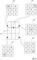
- Figure 8 illustrates a couple of examples of such a target usable for metrology and correction, where Figure 8(a) is an example of a focus metrology target and Figure 8(b) is an example of an overlay metrology target.
- the target comprises four pads 81, 81', 82, 82' of focus-sensitive gratings 85 (see example detail), paired two-by-two, forming two focus targets.
- the target also comprises four LS or grating calibration pads 83 comprising line-space gratings 86 (again example detail is shown) having the same pitch P and similar CD as the focus sensitive gratings, but without the "comb" structures (sub-resolution features) on the reticle which makes the target exposed on the substrate therefrom focus sensitive.
- the target further comprises a central reflective calibration pad or empty calibration pad 84 (labeled O) which comprises no diffracting structures.
- the focus pads comprise a first pair of mirrored (mutually reversed) pads 81, 81' and a second pair of mirrored pads 82, 82'.
- One or more of the grating feature parameters w 1 , w 2 w 3 is/are varied between the two pairs of mirrored pads, while the pitch P is not varied.
- the basic principle of how the focus pads work and how focus is inferred from them has been described and will not be described further.
- the focus inference detail, number of focus pads and specific form of each focus pad is not relevant to the concept of this disclosure in any case, and the number of focus pads and/or their basic form may differ from illustrated here.
- FIG 8(b) illustrates an equivalent overlay target.
- the focus pads are replaced with overlay pads 32, 33, 34, 35 which each may have the same form as its corresponding overlay pad 32, 33, 34, 35 in Figure 6 (a conventional ⁇ DBO overlay target).
- the overlay gratings of the pads may have the same pitch as that of the gratings of the LS pads; however the overlay gratings are compound gratings formed in two layers, typically but optionally with a bias (e.g., biases +d, -d).
- overlay targets in the two directions of the substrate plane may be provided.
- the overlay inference detail, number of overlay pads and specific form of each overlay pad is not relevant to the concept of this disclosure, and the number of overlay pads and/or their basic form may differ from illustrated here.
- the intensity of the LS calibration pad(s) 83 and (where applicable) empty calibration pad(s) 84 are captured at the same time (e.g. within the same acquisition) and therefore with the same acquisition settings as the other sub-targets.
- the target disclosed herein may be measured in a single acquisition as is the case with present multi-pad targets (e.g., such as the overlay target illustrated in Figure 6 , the single acquisition measurement of which is illustrated in Figure7 ). This may be the case for measurements at all the metrology points of the wafer.
- any asymmetry measured on them is a result of the sensor (sensor asymmetry) or process artifacts.
- This automatically provides sufficient data to compute a position-dependent sensor asymmetry correction (or tool asymmetry correction) with full wafer density and without additional overhead time. This correction can be applied to the parameter of interest inference in real time.
- the method may comprise measuring the asymmetry in the measured signal from at least one LS calibration pad 83 per target and attributing this asymmetry to sensor asymmetry. This can then be used as a sensor asymmetry correction used to correct (e.g., to subtract from) measurements from the main metrology pads (e.g., overlay or focus pads). This can be done for each target at different locations over the wafer. In this way, the position-dependent sensor asymmetry effect can be corrected.
- the main metrology pads e.g., overlay or focus pads
- an intensity value may be determined for each of the LS calibration pads 83, which will be in different positions within the measurement spot during an acquisition. This allows an intensity map to be determined, from which scaling corrections can be applied to the focus or overlay sensitive gratings in order to cancel out the effect of spot inhomogeneity issues.
- the same measurement data from the LS calibration pads can also be used to detect (e.g., small) process variations that cause variations in the total light diffracted by the grating. Since the LS calibration pads are not focus or overlay sensitive (or, at least, much less sensitive than the real targets) a (e.g., spatial) variation in the measured intensity from these pads will be directly related to a process variation, and as such this variation can be measured and process variation detected. Additionally, for added precision, the intensities of multiple neighboring LS calibration pads (for example, within the same field) can be averaged, since the spatial frequency of the process variations is larger than the typical density of the targets within the field. It would be impossible to do this with conventional monitoring key performance indicators (KPIs) which use intensities from the parameter of interest sensitive targets because the signal of the process variation will be masked by the intrafield variations of the parameter of interest.
- KPIs monitoring key performance indicators
- the empty pad(s) 84 does not contain any structure, it should not produce any intensity in the dark field image, for which the zeroth order (specularly reflected) radiation is blocked and the image comprises only higher order diffracted radiation. Any residual intensity measured in this location corresponds to ghost intensity. As such, a measurement of this residual intensity of the image portion corresponding to the empty pad can be used as a ghost correction (e.g., can be subtracted from the parameter of interest pad measurements).
- Intensity uniformity may be determined across the images of the calibration gratings (either or both types of the calibration gratings 83, 84) in order to detect possible parallax effects. Since these pads are not focus or overlay dependent, its intensity variation across the wafer should be small (mostly driven by process variations). Therefore an intensity map from the calibration targets may be determined from all the wafer locations, and any steep intensity changes (e.g., above a threshold change) may be detected, which would indicate the presence of parallax effect.
- the positions of the calibration pads within the target may be varied with intrafield position.
- a reticle used to pattern these targets may be designed in such way that different intrafield locations may comprise one or more calibration gratings (of either or both types described herein) in different locations. This may enable, for example, a more detailed mapping of the spot inhomogeneity and ghost intensity distributions, as more positions within the measurement spot may be sampled. It also means that each individual target can have fewer calibration targets while still being able to characterize spot inhomogeneity properly, for example. This can save on reticle/substrate real-estate and/or allow for more actual metrology pads (parameter of interest sensitive pads) per target.
- Figure 9 illustrates an example of such an embodiment.
- the Figure shows schematically a field 90, here comprising 9 dies 91.
- the field in this example has five metrology points, each comprising a target 92a, 92b, 92c, 92d, 92e.
- each target comprises eight parameter of interest sensitive pads (in this specific example, focus pads) which allow for more target combinations in order to increase accuracy in inferring the parameter of interest and one LS calibration pad, which is located at a different position within the target at each intrafield location. This allows for an average mapping of spot inhomogeneity while maximizing the space on the target dedicated to parameter of interest sensitive gratings.
- a target concept which enables calibration, correction and/or monitoring of issues such as spot inhomogeneity, (e.g., internal and external) ghost calibration, sensor asymmetry, stack cross-talk, and parallax effects without any wafer overhead or throughput reduction.
- the target may be measured in a single acquisition. Corrections can be made with full wafer density and measured with exactly the same acquisition settings and same stack as for the actual paramter of interest measurements. Direct qualitative wafer maps of process variation can be made from such targets. Calibration data can be obtained over whole wafer (all metrology points), therefore correction may be position dependent, e.g., interfield and intrafield.
- lithographic apparatus in the manufacture of ICs, it should be understood that the lithographic apparatus described herein may have other applications. Possible other applications include the manufacture of integrated optical systems, guidance and detection patterns for magnetic domain memories, flat-panel displays, liquid-crystal displays (LCDs), thin-film magnetic heads, etc.
- Embodiments of the invention may form part of a mask inspection apparatus, a metrology apparatus, or any apparatus that measures or processes an object such as a wafer (or other substrate) or mask (or other patterning device). These apparatus may be generally referred to as lithographic tools. Such a lithographic tool may use vacuum conditions or ambient (non-vacuum) conditions.
Landscapes
- Physics & Mathematics (AREA)
- General Physics & Mathematics (AREA)
- Exposure And Positioning Against Photoresist Photosensitive Materials (AREA)
- Radar Systems Or Details Thereof (AREA)
- Length Measuring Devices By Optical Means (AREA)
- Crystals, And After-Treatments Of Crystals (AREA)
Priority Applications (7)
| Application Number | Priority Date | Filing Date | Title |
|---|---|---|---|
| EP21200798.3A EP4160314A1 (fr) | 2021-10-04 | 2021-10-04 | Procédé de mesure d'au moins une cible sur un substrat |
| PCT/EP2022/076524 WO2023057237A1 (fr) | 2021-10-04 | 2022-09-23 | Procédé de mesure d'au moins une cible sur un substrat |
| CN202280065811.2A CN118020030A (zh) | 2021-10-04 | 2022-09-23 | 测量衬底上的至少一个目标的方法 |
| IL311582A IL311582A (en) | 2021-10-04 | 2022-09-23 | A method for measuring at least one target on a substrate |
| KR1020247011088A KR20240070563A (ko) | 2021-10-04 | 2022-09-23 | 기판 상의 적어도 하나의 타겟을 측정하는 방법 |
| TW111137455A TWI823593B (zh) | 2021-10-04 | 2022-10-03 | 用於測量基板上的至少一個目標的方法及相關聯設備和基板 |
| TW112138945A TWI850127B (zh) | 2021-10-04 | 2022-10-03 | 用於測量基板上的至少一個目標的方法及相關聯設備和基板 |
Applications Claiming Priority (1)
| Application Number | Priority Date | Filing Date | Title |
|---|---|---|---|
| EP21200798.3A EP4160314A1 (fr) | 2021-10-04 | 2021-10-04 | Procédé de mesure d'au moins une cible sur un substrat |
Publications (1)
| Publication Number | Publication Date |
|---|---|
| EP4160314A1 true EP4160314A1 (fr) | 2023-04-05 |
Family
ID=78073865
Family Applications (1)
| Application Number | Title | Priority Date | Filing Date |
|---|---|---|---|
| EP21200798.3A Withdrawn EP4160314A1 (fr) | 2021-10-04 | 2021-10-04 | Procédé de mesure d'au moins une cible sur un substrat |
Country Status (6)
| Country | Link |
|---|---|
| EP (1) | EP4160314A1 (fr) |
| KR (1) | KR20240070563A (fr) |
| CN (1) | CN118020030A (fr) |
| IL (1) | IL311582A (fr) |
| TW (2) | TWI823593B (fr) |
| WO (1) | WO2023057237A1 (fr) |
Citations (10)
| Publication number | Priority date | Publication date | Assignee | Title |
|---|---|---|---|---|
| US20050185174A1 (en) * | 2004-02-23 | 2005-08-25 | Asml Netherlands B.V. | Method to determine the value of process parameters based on scatterometry data |
| US6952253B2 (en) | 2002-11-12 | 2005-10-04 | Asml Netherlands B.V. | Lithographic apparatus and device manufacturing method |
| EP1628164A2 (fr) | 2004-08-16 | 2006-02-22 | ASML Netherlands B.V. | Procédé et dispositif pour caractérisation de la lithographie par spectrométrie à résolution angulaire |
| US20060132744A1 (en) * | 2004-12-21 | 2006-06-22 | Asml Netherlands B.V. | Lithographic apparatus focus test method and system, and device manufacturing method |
| US20100328655A1 (en) | 2007-12-17 | 2010-12-30 | Asml, Netherlands B.V. | Diffraction Based Overlay Metrology Tool and Method |
| US20110026032A1 (en) | 2008-04-09 | 2011-02-03 | Asml Netherland B.V. | Method of Assessing a Model of a Substrate, an Inspection Apparatus and a Lithographic Apparatus |
| US20110102753A1 (en) | 2008-04-21 | 2011-05-05 | Asml Netherlands B.V. | Apparatus and Method of Measuring a Property of a Substrate |
| US20110249244A1 (en) | 2008-10-06 | 2011-10-13 | Asml Netherlands B.V. | Lithographic Focus and Dose Measurement Using A 2-D Target |
| US20120044470A1 (en) | 2010-08-18 | 2012-02-23 | Asml Netherlands B.V. | Substrate for Use in Metrology, Metrology Method and Device Manufacturing Method |
| US20180373167A1 (en) * | 2016-10-25 | 2018-12-27 | Kla-Tencor Corporation | Fault Discrimination and Calibration of Scatterometry Overlay Targets |
Family Cites Families (2)
| Publication number | Priority date | Publication date | Assignee | Title |
|---|---|---|---|---|
| KR102370347B1 (ko) * | 2017-02-02 | 2022-03-04 | 에이에스엠엘 네델란즈 비.브이. | 메트롤로지 방법 및 장치 및 연계된 컴퓨터 제품 |
| NL2021852A (en) * | 2018-08-01 | 2018-11-09 | Asml Netherlands Bv | Metrology apparatus and method for determining a characteristic of one or more structures on a substrate |
-
2021
- 2021-10-04 EP EP21200798.3A patent/EP4160314A1/fr not_active Withdrawn
-
2022
- 2022-09-23 IL IL311582A patent/IL311582A/en unknown
- 2022-09-23 KR KR1020247011088A patent/KR20240070563A/ko unknown
- 2022-09-23 WO PCT/EP2022/076524 patent/WO2023057237A1/fr active Application Filing
- 2022-09-23 CN CN202280065811.2A patent/CN118020030A/zh active Pending
- 2022-10-03 TW TW111137455A patent/TWI823593B/zh active
- 2022-10-03 TW TW112138945A patent/TWI850127B/zh active
Patent Citations (10)
| Publication number | Priority date | Publication date | Assignee | Title |
|---|---|---|---|---|
| US6952253B2 (en) | 2002-11-12 | 2005-10-04 | Asml Netherlands B.V. | Lithographic apparatus and device manufacturing method |
| US20050185174A1 (en) * | 2004-02-23 | 2005-08-25 | Asml Netherlands B.V. | Method to determine the value of process parameters based on scatterometry data |
| EP1628164A2 (fr) | 2004-08-16 | 2006-02-22 | ASML Netherlands B.V. | Procédé et dispositif pour caractérisation de la lithographie par spectrométrie à résolution angulaire |
| US20060132744A1 (en) * | 2004-12-21 | 2006-06-22 | Asml Netherlands B.V. | Lithographic apparatus focus test method and system, and device manufacturing method |
| US20100328655A1 (en) | 2007-12-17 | 2010-12-30 | Asml, Netherlands B.V. | Diffraction Based Overlay Metrology Tool and Method |
| US20110026032A1 (en) | 2008-04-09 | 2011-02-03 | Asml Netherland B.V. | Method of Assessing a Model of a Substrate, an Inspection Apparatus and a Lithographic Apparatus |
| US20110102753A1 (en) | 2008-04-21 | 2011-05-05 | Asml Netherlands B.V. | Apparatus and Method of Measuring a Property of a Substrate |
| US20110249244A1 (en) | 2008-10-06 | 2011-10-13 | Asml Netherlands B.V. | Lithographic Focus and Dose Measurement Using A 2-D Target |
| US20120044470A1 (en) | 2010-08-18 | 2012-02-23 | Asml Netherlands B.V. | Substrate for Use in Metrology, Metrology Method and Device Manufacturing Method |
| US20180373167A1 (en) * | 2016-10-25 | 2018-12-27 | Kla-Tencor Corporation | Fault Discrimination and Calibration of Scatterometry Overlay Targets |
Also Published As
| Publication number | Publication date |
|---|---|
| TW202403470A (zh) | 2024-01-16 |
| TW202328823A (zh) | 2023-07-16 |
| WO2023057237A1 (fr) | 2023-04-13 |
| TWI850127B (zh) | 2024-07-21 |
| IL311582A (en) | 2024-05-01 |
| KR20240070563A (ko) | 2024-05-21 |
| TWI823593B (zh) | 2023-11-21 |
| CN118020030A (zh) | 2024-05-10 |
Similar Documents
| Publication | Publication Date | Title |
|---|---|---|
| KR102066588B1 (ko) | 검사 장치, 검사 방법, 리소그래피 장치, 패터닝 디바이스 및 제조 방법 | |
| US9910366B2 (en) | Metrology method and apparatus, lithographic system and device manufacturing method | |
| US20150145151A1 (en) | Metrology Method and Apparatus, Lithographic System, Device Manufacturing Method and Substrate | |
| CN111133384B (zh) | 用于确定图案化过程参数的方法 | |
| TWI752647B (zh) | 用於推斷例如聚焦之處理參數之方法與相關聯之設備及製造方法 | |
| US10317805B2 (en) | Method for monitoring a characteristic of illumination from a metrology apparatus | |
| US20240036484A1 (en) | Method of metrology and associated apparatuses | |
| US20230176491A1 (en) | A substrate comprising a target arrangement, and associated at least one patterning device, lithographic method and metrology method | |
| US20230035073A1 (en) | Method for determining a measurement recipe and associated apparatuses | |
| EP4160314A1 (fr) | Procédé de mesure d'au moins une cible sur un substrat | |
| TWI825933B (zh) | 判定量測配方之方法及其相關設備 | |
| EP4155821A1 (fr) | Procédé de métrologie focalisée et appareils associés | |
| EP4191338A1 (fr) | Procédé d'étalonnage de métrologie | |
| EP4194952A1 (fr) | Procédé pour déterminer une recette de mesure et appareils associés | |
| US20220100107A1 (en) | Alignment method and associated metrology device | |
| WO2024033036A1 (fr) | Procédé de métrologie et dispositif de métrologie associé | |
| WO2024033035A1 (fr) | Procédé de métrologie et dispositif de métrologie associé | |
| WO2024153591A1 (fr) | Procédé et appareil de détermination de performances de processus de formation de motifs | |
| NL2022659A (en) | Alignment method and associated metrology device |
Legal Events
| Date | Code | Title | Description |
|---|---|---|---|
| PUAI | Public reference made under article 153(3) epc to a published international application that has entered the european phase |
Free format text: ORIGINAL CODE: 0009012 |
|
| STAA | Information on the status of an ep patent application or granted ep patent |
Free format text: STATUS: THE APPLICATION HAS BEEN PUBLISHED |
|
| AK | Designated contracting states |
Kind code of ref document: A1 Designated state(s): AL AT BE BG CH CY CZ DE DK EE ES FI FR GB GR HR HU IE IS IT LI LT LU LV MC MK MT NL NO PL PT RO RS SE SI SK SM TR |
|
| STAA | Information on the status of an ep patent application or granted ep patent |
Free format text: STATUS: THE APPLICATION IS DEEMED TO BE WITHDRAWN |
|
| 18D | Application deemed to be withdrawn |
Effective date: 20231006 |